CN101416302A - Elastically deformable integrated circuit devices - Google Patents
Elastically deformable integrated circuit devicesDownload PDFInfo
- Publication number
- CN101416302A CN101416302ACNA200780012607XACN200780012607ACN101416302ACN 101416302 ACN101416302 ACN 101416302ACN A200780012607X ACNA200780012607X ACN A200780012607XACN 200780012607 ACN200780012607 ACN 200780012607ACN 101416302 ACN101416302 ACN 101416302A
- Authority
- CN
- China
- Prior art keywords
- elastically deformable
- substrate island
- integrated circuit
- components
- separately
- Prior art date
- Legal status (The legal status is an assumption and is not a legal conclusion. Google has not performed a legal analysis and makes no representation as to the accuracy of the status listed.)
- Pending
Links
Images


Classifications
- H—ELECTRICITY
- H05—ELECTRIC TECHNIQUES NOT OTHERWISE PROVIDED FOR
- H05K—PRINTED CIRCUITS; CASINGS OR CONSTRUCTIONAL DETAILS OF ELECTRIC APPARATUS; MANUFACTURE OF ASSEMBLAGES OF ELECTRICAL COMPONENTS
- H05K1/00—Printed circuits
- H05K1/02—Details
- H05K1/0277—Bendability or stretchability details
- H05K1/0283—Stretchable printed circuits
- H—ELECTRICITY
- H01—ELECTRIC ELEMENTS
- H01L—SEMICONDUCTOR DEVICES NOT COVERED BY CLASS H10
- H01L23/00—Details of semiconductor or other solid state devices
- H01L23/52—Arrangements for conducting electric current within the device in operation from one component to another, i.e. interconnections, e.g. wires, lead frames
- H01L23/538—Arrangements for conducting electric current within the device in operation from one component to another, i.e. interconnections, e.g. wires, lead frames the interconnection structure between a plurality of semiconductor chips being formed on, or in, insulating substrates
- H01L23/5387—Flexible insulating substrates
- H—ELECTRICITY
- H01—ELECTRIC ELEMENTS
- H01L—SEMICONDUCTOR DEVICES NOT COVERED BY CLASS H10
- H01L24/00—Arrangements for connecting or disconnecting semiconductor or solid-state bodies; Methods or apparatus related thereto
- H01L24/01—Means for bonding being attached to, or being formed on, the surface to be connected, e.g. chip-to-package, die-attach, "first-level" interconnects; Manufacturing methods related thereto
- H—ELECTRICITY
- H01—ELECTRIC ELEMENTS
- H01L—SEMICONDUCTOR DEVICES NOT COVERED BY CLASS H10
- H01L25/00—Assemblies consisting of a plurality of semiconductor or other solid state devices
- H01L25/03—Assemblies consisting of a plurality of semiconductor or other solid state devices all the devices being of a type provided for in a single subclass of subclasses H10B, H10D, H10F, H10H, H10K or H10N, e.g. assemblies of rectifier diodes
- H01L25/04—Assemblies consisting of a plurality of semiconductor or other solid state devices all the devices being of a type provided for in a single subclass of subclasses H10B, H10D, H10F, H10H, H10K or H10N, e.g. assemblies of rectifier diodes the devices not having separate containers
- H01L25/065—Assemblies consisting of a plurality of semiconductor or other solid state devices all the devices being of a type provided for in a single subclass of subclasses H10B, H10D, H10F, H10H, H10K or H10N, e.g. assemblies of rectifier diodes the devices not having separate containers the devices being of a type provided for in group H10D89/00
- H01L25/0655—Assemblies consisting of a plurality of semiconductor or other solid state devices all the devices being of a type provided for in a single subclass of subclasses H10B, H10D, H10F, H10H, H10K or H10N, e.g. assemblies of rectifier diodes the devices not having separate containers the devices being of a type provided for in group H10D89/00 the devices being arranged next to each other
- H—ELECTRICITY
- H01—ELECTRIC ELEMENTS
- H01L—SEMICONDUCTOR DEVICES NOT COVERED BY CLASS H10
- H01L2924/00—Indexing scheme for arrangements or methods for connecting or disconnecting semiconductor or solid-state bodies as covered by H01L24/00
- H01L2924/10—Details of semiconductor or other solid state devices to be connected
- H01L2924/11—Device type
- H01L2924/14—Integrated circuits
- H—ELECTRICITY
- H01—ELECTRIC ELEMENTS
- H01L—SEMICONDUCTOR DEVICES NOT COVERED BY CLASS H10
- H01L2924/00—Indexing scheme for arrangements or methods for connecting or disconnecting semiconductor or solid-state bodies as covered by H01L24/00
- H01L2924/30—Technical effects
- H01L2924/35—Mechanical effects
- H01L2924/351—Thermal stress
- H—ELECTRICITY
- H05—ELECTRIC TECHNIQUES NOT OTHERWISE PROVIDED FOR
- H05K—PRINTED CIRCUITS; CASINGS OR CONSTRUCTIONAL DETAILS OF ELECTRIC APPARATUS; MANUFACTURE OF ASSEMBLAGES OF ELECTRICAL COMPONENTS
- H05K2201/00—Indexing scheme relating to printed circuits covered by H05K1/00
- H05K2201/01—Dielectrics
- H05K2201/0104—Properties and characteristics in general
- H05K2201/0133—Elastomeric or compliant polymer
- H—ELECTRICITY
- H05—ELECTRIC TECHNIQUES NOT OTHERWISE PROVIDED FOR
- H05K—PRINTED CIRCUITS; CASINGS OR CONSTRUCTIONAL DETAILS OF ELECTRIC APPARATUS; MANUFACTURE OF ASSEMBLAGES OF ELECTRICAL COMPONENTS
- H05K2201/00—Indexing scheme relating to printed circuits covered by H05K1/00
- H05K2201/09—Shape and layout
- H05K2201/09209—Shape and layout details of conductors
- H05K2201/09218—Conductive traces
- H05K2201/09263—Meander
- H—ELECTRICITY
- H05—ELECTRIC TECHNIQUES NOT OTHERWISE PROVIDED FOR
- H05K—PRINTED CIRCUITS; CASINGS OR CONSTRUCTIONAL DETAILS OF ELECTRIC APPARATUS; MANUFACTURE OF ASSEMBLAGES OF ELECTRICAL COMPONENTS
- H05K2201/00—Indexing scheme relating to printed circuits covered by H05K1/00
- H05K2201/09—Shape and layout
- H05K2201/09209—Shape and layout details of conductors
- H05K2201/09654—Shape and layout details of conductors covering at least two types of conductors provided for in H05K2201/09218 - H05K2201/095
- H05K2201/09781—Dummy conductors, i.e. not used for normal transport of current; Dummy electrodes of components
- H—ELECTRICITY
- H05—ELECTRIC TECHNIQUES NOT OTHERWISE PROVIDED FOR
- H05K—PRINTED CIRCUITS; CASINGS OR CONSTRUCTIONAL DETAILS OF ELECTRIC APPARATUS; MANUFACTURE OF ASSEMBLAGES OF ELECTRICAL COMPONENTS
- H05K2203/00—Indexing scheme relating to apparatus or processes for manufacturing printed circuits covered by H05K3/00
- H05K2203/01—Tools for processing; Objects used during processing
- H05K2203/0147—Carriers and holders
- H05K2203/016—Temporary inorganic, non-metallic carrier, e.g. for processing or transferring
- H—ELECTRICITY
- H05—ELECTRIC TECHNIQUES NOT OTHERWISE PROVIDED FOR
- H05K—PRINTED CIRCUITS; CASINGS OR CONSTRUCTIONAL DETAILS OF ELECTRIC APPARATUS; MANUFACTURE OF ASSEMBLAGES OF ELECTRICAL COMPONENTS
- H05K2203/00—Indexing scheme relating to apparatus or processes for manufacturing printed circuits covered by H05K3/00
- H05K2203/02—Details related to mechanical or acoustic processing, e.g. drilling, punching, cutting, using ultrasound
- H05K2203/0271—Mechanical force other than pressure, e.g. shearing or pulling
- H—ELECTRICITY
- H05—ELECTRIC TECHNIQUES NOT OTHERWISE PROVIDED FOR
- H05K—PRINTED CIRCUITS; CASINGS OR CONSTRUCTIONAL DETAILS OF ELECTRIC APPARATUS; MANUFACTURE OF ASSEMBLAGES OF ELECTRICAL COMPONENTS
- H05K3/00—Apparatus or processes for manufacturing printed circuits
- H05K3/007—Manufacture or processing of a substrate for a printed circuit board supported by a temporary or sacrificial carrier
Landscapes
- Engineering & Computer Science (AREA)
- Microelectronics & Electronic Packaging (AREA)
- Computer Hardware Design (AREA)
- Power Engineering (AREA)
- Physics & Mathematics (AREA)
- Condensed Matter Physics & Semiconductors (AREA)
- General Physics & Mathematics (AREA)
- Internal Circuitry In Semiconductor Integrated Circuit Devices (AREA)
- Semiconductor Integrated Circuits (AREA)
- Reduction Or Emphasis Of Bandwidth Of Signals (AREA)
Abstract
Description
Translated fromChinese技术领域technical field
本发明涉及一种集成电路器件,这种集成电路器件包括多个分离的刚性衬底岛,这些衬底岛带有电路元件,各自的衬底岛通过各自的可弹性变形的连接连接到各自的相邻的衬底岛,这些可弹性变形的连接含有至少一个各自的信令层,这种信令层用导电材料制成。The present invention relates to an integrated circuit device comprising a plurality of separate rigid substrate islands carrying circuit elements, the respective substrate islands being connected by respective elastically deformable connections to respective Adjacent to the substrate islands, these elastically deformable connections contain at least one respective signaling layer made of electrically conductive material.
背景技术Background technique
这些柔性集成电路器件在下面也称为柔性电路或柔性电路类型的集成电路器件,并且可从US 6,479,890 B1和US 6,617671 B1获知。在这些柔性电路中,刚性衬底岛形成柔性网络或网,这些刚性衬底岛包括电路元件和这些电路元件之间的可弹性变形的连接,这些连接提供用于衬底岛之间的信号交换的信令层。柔性电路能够容许弯曲移动以及由这些移动所导致的拉伸应力和压力,而保持电路的完整性。相反,单晶硅既硬又脆,且往往通过破裂产生机械应力,这就降低产量并缩短集成电路器件的产品寿命。These flexible integrated circuit devices are also referred to below as flexible circuits or integrated circuit devices of the flexible circuit type and are known from US 6,479,890 B1 and US 6,617671 B1. In these flexible circuits, rigid substrate islands form a flexible network or net, these rigid substrate islands include circuit elements and elastically deformable connections between these circuit elements, these connections provide for the exchange of signals between the substrate islands signaling layer. Flexible circuits are able to tolerate bending movements and the tensile stresses and pressures caused by these movements while maintaining the integrity of the circuit. In contrast, single crystal silicon is hard and brittle, and tends to generate mechanical stress through cracking, which reduces yield and shortens the product lifetime of integrated circuit devices.
柔性电路还提供其它特定优点。例如,这些柔性电路可具有可从毫米至米调节的延伸件。这样就可用有成本效率的方式设计大面积器件。Flexible circuits also offer other specific advantages. For example, these flex circuits may have extensions that are adjustable from millimeters to meters. This allows the design of large area devices in a cost-effective manner.
不过,已知可弹性变形的连接中的信令层可含有高水平机械应力,例如,这些信令层用钛(Ti)、氮化钛(TiN)或铜(Cu)制成。例如,这种应力在制造过程中的热循环期间产生并由信令层与相邻的绝缘体之间的热膨胀系数(CTE)的失配所导致。这种应力还可以是这些连接中的主要应力作用,且大于由这种器件的理想的延伸、压力或弯曲为了应用目的而产生的应力作用。However, it is known that signaling layers in elastically deformable connections, eg made of titanium (Ti), titanium nitride (TiN) or copper (Cu), may contain high levels of mechanical stress. For example, such stresses arise during thermal cycling in the manufacturing process and result from a mismatch in the coefficient of thermal expansion (CTE) between the signaling layer and the adjacent insulator. This stress can also be the dominant stress contribution in these connections and be greater than that produced by ideal extension, compression or bending of the device for application purposes.
不均匀的应力在US 6,479,890 B1(Trieu等人)中所公开的集成电路器件中增加,在这种器件中,一些相邻的衬底岛对由柔性箔连接,这种柔性箔含有一个信令层,而其它的衬底岛含有平行布置的两个或更多的信令层。可在形成集成电路器件的柔性网中产生并不希望的不均匀应力分布,这些不均匀应力分布在最糟的情况下导致连接的破裂。这不利于器件性能。例如,在传感器用途中,含有这些传感器的衬底岛的规则隔开的布置是理想的,且单个衬底岛的错误定位或仅有一些连接的故障降低器件的可靠性。Inhomogeneous stresses are increased in integrated circuit devices disclosed in US 6,479,890 B1 (Trieu et al.), in which pairs of adjacent substrate islands are connected by flexible foils containing a signaling layers, while other substrate islands contain two or more signaling layers arranged in parallel. Undesirable non-uniform stress distributions can be created in the flexible web forming the integrated circuit device, which in the worst case can lead to cracking of the connections. This is detrimental to device performance. For example, in sensor applications, a regularly spaced arrangement of substrate islands containing these sensors is desirable, and mispositioning of individual substrate islands or failure of only a few connections reduces device reliability.
另一方面,像US 6,617671 B1那样在相邻的衬底岛之间含有相等数量的信令层的柔性连接制约了电路设计的自由度,并且将柔性电路的适用性限制在在衬底岛之间具有相同的布线的情形中。On the other hand, flex connections with an equal number of signaling layers between adjacent substrate islands like US 6,617671 B1 restrict the freedom of circuit design and limit the applicability of flex circuits to substrate In the case of identical routing between islands.
发明内容Contents of the invention
因此,本发明的目的在于提供一种柔性电路类型的集成电路器件,这种集成电路器件具有减少的不均匀应力分布并允许衬底岛之间的电气连接的复杂图案。It is therefore an object of the present invention to provide an integrated circuit device of the flexible circuit type which has reduced non-uniform stress distribution and which allows complex patterns of electrical connections between islands of the substrate.
根据本发明的第一方面,集成电路器件包括多个分离的刚性衬底岛,这些衬底岛带有电路元件。各自的衬底岛通过各自的可弹性变形的连接连接到各自的相邻的衬底岛。这些可弹性变形的连接含有至少一个各自的信令层,这种信令层用导电材料制成。在本发明的集成电路器件中,在衬底岛之间的至少一个可弹性变形的连接具有信令层,这种信令层并不电气连接并因此而形成虚设信令层。而且,这些可弹性变形的连接沿着第一方向将各自的衬底岛连接到各自的相邻的衬底岛并具有以该第一方向的可弹性变形性,这种可弹性变形性由各自的弹性模量所主导,这种弹性模量的比率介于0.5与2.0之间。According to a first aspect of the invention, an integrated circuit device includes a plurality of separate rigid substrate islands carrying circuit elements. A respective substrate island is connected to a respective adjacent substrate island by a respective elastically deformable connection. These elastically deformable connections contain at least one respective signaling layer made of electrically conductive material. In the integrated circuit device according to the invention, at least one elastically deformable connection between the substrate islands has a signaling layer which is not electrically connected and thus forms a dummy signaling layer. Furthermore, the elastically deformable connections connect a respective substrate island to a respective adjacent substrate island along a first direction and have elastic deformability in the first direction, which elastic deformability is determined by the respective Dominated by the modulus of elasticity, the ratio of this modulus of elasticity is between 0.5 and 2.0.
本发明的集成电路器件具有可弹性变形的连接,这些连接具有以该第一方向的可弹性变形性,这种可弹性变形性由各自的弹性模量所主导,这种弹性模量的比率介于0.5与2.0之间。这就意味着任何对的以该第一方向的可弹性变形的连接具有介于1/2与2/1之间的比率。也将具有在这种间隔之内的比率的弹性模量称为平衡弹性模量。弹性模量的这些比率的限制与提供至少一个虚设信令层的概念有关。为了提供与所提及的弹性模量配合的至少一个虚设信令层,在前面所提及的限制内的比率平衡这些可弹性变形的连接,而并不考虑这些衬底岛的电路元件之间的电气连通性的特别要求。虚设信令层可用于平衡弹性模量比率,而无需电气连接。本发明可用于选择适当数量的虚设信令层,以在特定电路设计的所要求的电气连接往往单独提供这种平衡可弹性变形性的情形中平衡不同的可弹性变形的连接的可弹性变形性。The integrated circuit device of the present invention has elastically deformable connections having elastic deformability in the first direction, the elastic deformability being dominated by respective elastic moduli, the ratio of which is between Between 0.5 and 2.0. This means that any pair of elastically deformable connections in the first direction has a ratio comprised between 1/2 and 2/1. A modulus of elasticity having a ratio within such an interval is also referred to as an equilibrium modulus of elasticity. The limitation of these ratios of elastic moduli is related to the concept of providing at least one dummy signaling layer. In order to provide at least one dummy signaling layer compatible with the mentioned elastic moduli, the ratios within the previously mentioned limits balance the elastically deformable connections without regard to the circuit elements between the substrate islands special requirements for electrical connectivity. A dummy signaling layer can be used to balance the elastic modulus ratio without the need for electrical connections. The present invention can be used to select an appropriate number of dummy signaling layers to balance the elastic deformability of different elastically deformable connections in situations where the required electrical connections of a particular circuit design tend to provide such balanced elastic deformability alone .
本发明的集成电路器件还具有允许提供用于多种类型的柔性电路的平衡可弹性变形连接的标准设计而并不考虑这些连接的单独的功能度和电路要求的优点。所有的连接可含有相等数量的信令层,且柔性电路的特别应用的单独设计的唯一问题是连接或不连接单独的信令层。可制造或省略这些信令层的这些电气连接,而并不对可弹性变形的连接的弹性模量造成太大影响。虚设信令层可由电气绝缘材料的小段终结。The integrated circuit device of the present invention also has the advantage of allowing the provision of a standard design of balanced elastically deformable connections for multiple types of flexible circuits regardless of the individual functionality and circuit requirements of these connections. All connections may contain an equal number of signaling layers, and the only issue for the individual design of a particular application of the flexible circuit is to connect or not connect separate signaling layers. These electrical connections of the signaling layers can be made or omitted without too much impact on the modulus of elasticity of the elastically deformable connections. The dummy signaling layer may be terminated by a small section of electrically insulating material.
这种弹性模量也称为扬氏模量。这两种术语同时用在本说明书中并具有相同的意义。将弹性模量或扬氏模量限定为对随着应变的应力变化率的小应变的限制。对于许多材料而言,扬氏模量在应变范围内恒定,以使这些应变遵守胡克定律。不过,在非线性材料中,扬氏模量随着应变的变动而变化。出于本发明的目的,在与应用目的有关的整个间隔内足以确保平衡这些可弹性变形的连接的扬氏模量。大于应变情形而言,不必考虑扬氏模量的比率,这些应变情形与这种器件的制造或运行无关。This modulus of elasticity is also called Young's modulus. These two terms are used simultaneously in this specification and have the same meaning. The modulus of elasticity or Young's modulus is defined as the limit of small strains on the rate of change of stress with strain. For many materials, Young's modulus is constant over a range of strains such that these strains obey Hooke's law. However, in nonlinear materials, Young's modulus varies with strain. For the purposes of the present invention, it is sufficient to ensure a balanced Young's modulus of these elastically deformable connections over the entire interval relevant to the purpose of the application. The ratio of Young's modulus need not be considered for strain cases greater than those that are not relevant to the fabrication or operation of such devices.
弹性模量或扬氏模量是一种张量。可弹性变形的连接可各向异性,即可具有不同的扬氏模量值并因此而对以不同方向所加的应力展示出不同的机械性能。出于本发明的目的,确保平衡这些可弹性变形的连接的扬氏模量以用于与应用目的有关的方向就已足够。换言之,这些可弹性变形的连接可具有不同的扬氏模量值。The modulus of elasticity or Young's modulus is a tensor. Elastically deformable connections may be anisotropic, ie have different values of Young's modulus and thus exhibit different mechanical properties for stresses applied in different directions. For the purposes of the present invention, it is sufficient to ensure that the Young's moduli of these elastically deformable connections are balanced for directions relevant to the purpose of the application. In other words, the elastically deformable connections can have different Young's modulus values.
由于这些电桥的弹性模量主导回应于机械应力的这些柔性电路中的应变分布,所以具有相同的弹性模量的可弹性变形的连接以相同的方式产生相同的应力,从而降低由这种柔性电路所形成的网络中的应变的不均匀性。这样,与现有技术中的器件相比,本发明的集成电路器件的功能可靠性就得到了提高。Since the modulus of elasticity of the bridges dominates the strain distribution in these flex circuits in response to mechanical stress, elastically deformable connections with the same modulus of elasticity produce the same stress in the same way, thereby reducing the stress caused by this flexibility. Inhomogeneity of strain in a network formed by an electrical circuit. Thus, the functional reliability of the integrated circuit device of the present invention is increased compared to prior art devices.
由于制造误差的原因,集成电路器件的不同可弹性变形的连接之间的弹性模量的轻微偏差不可避免。因此,对于集成电路器件的所有电桥而言,完全相同的弹性模量值形成根据本发明的理想情形。不过,介于0.5至2.0之间的与这种理想情形的偏差在本发明的范围之内。在优选实施例中,弹性模量的比率介于0.67与1.5之间,甚至可在0.8与1.25之间。在本申请的范围内,为了保持描述不出现不必要的重复,在提及弹性模量的“相同”值时,介于0.5至2.0之间的所有实施例均与术语“平衡弹性模量”一致进行处理,除非另有明确说明。Slight deviations in the modulus of elasticity between different elastically deformable connections of an integrated circuit device are unavoidable due to manufacturing tolerances. Thus, for all bridges of the integrated circuit device, exactly the same value of the modulus of elasticity forms an ideal situation according to the invention. However, deviations from this ideal of between 0.5 and 2.0 are within the scope of the invention. In a preferred embodiment, the ratio of the modulus of elasticity is between 0.67 and 1.5, and may even be between 0.8 and 1.25. Within the scope of the present application, in order to keep the description from unnecessary repetition, when referring to the "same" value of the modulus of elasticity, all the examples between 0.5 and 2.0 are related to the term "equilibrium modulus of elasticity" Processed consistently, unless expressly stated otherwise.
用在本说明书中的术语“信令层”是指用导电材料制成的材料,而无论是否在实际上用于不同的衬底岛的电路元件之间的信令目的。The term "signaling layer" as used in this specification refers to a material made of conductive material, whether or not actually used for signaling purposes between circuit elements of different substrate islands.
将术语“可弹性变形的连接”解释为在两个衬底岛之间提供机械连接的任何可弹性变形结构。The term "elastically deformable connection" is to be interpreted as any elastically deformable structure providing a mechanical connection between two substrate islands.
可弹性变形的连接的“可变形性”涉及任何类型的机械变形。变形是由于力的施加而导致的可弹性变形的连接的形状相对于无应力状态的形状的变化。力可以是拉力(拉动)、压力(推动)、剪切力、弯曲或扭曲(扭转)而无限制。对于剪切力的情形而言,可用的弹性模量是剪切模量。"Deformability" of an elastically deformable connection refers to any type of mechanical deformation. Deformation is the change in shape of an elastically deformable connection relative to the shape of the unstressed state due to the application of force. The force can be tensile (pull), compressive (push), shear, bend or twist (twist) without limitation. For the case of shear force, the available modulus of elasticity is the shear modulus.
“弹性”可变形性是可逆变形的能力。当停止施加力时,可弹性变形的连接返回到其原始形状。"Elastic" deformability is the ability to deform reversibly. When the force is stopped, the elastically deformable link returns to its original shape.
注意,本发明并不排除电桥的塑性变形,塑性变形是一种不可逆变形。塑性可变形性和弹性可变形性通常共存并应用于不同的应力区域。这些电桥的塑性可变形性可形成对优选实施例中的电桥的机械性能有用的作用,在这些优选实施例中,可弹性变形的连接在受到超过阈值应力量的应力时不会弹性变形。这就允许使单个的岛在制造之后处于相互之间的较大距离,即使得这种器件可伸展。优选将这些可弹性变形的连接的材料和/或结构选择为在非弹性变形之后施加低于阈值应力量的应力时展示出剩余的可弹性变形性。Note that the present invention does not exclude the plastic deformation of the bridge, which is an irreversible deformation. Plastic deformability and elastic deformability often coexist and apply to different stress regions. The plastic deformability of these bridges can have a useful effect on the mechanical properties of the bridges in preferred embodiments where elastically deformable connections do not elastically deform when subjected to stress exceeding a threshold stress amount . This allows the individual islands to be at a greater distance from each other after fabrication, ie to make the device stretchable. The materials and/or structures of these elastically deformable connections are preferably selected to exhibit residual elastic deformability upon application of a stress below a threshold stress amount after inelastic deformation.
本发明提供一种用于柔性电路类型的集成电路器件的衬底岛之间的可弹性变形的连接的新式设计规则。第一设计优先是本发明的集成电路器件的衬底岛之间的可弹性变形的连接的平衡弹性模量。这种新式设计规则替代以前的在衬底岛的电路元件之间优先提供所要求的电气互连的法则。不过,遵循现有技术的设计规则不会产生扬氏模量的相同值,因为根据设在由电桥连接的两个各自的衬底岛上的电路之间的特定布线要求,不同的可弹性变形的连接通常含有不同数量的互连,即不同数量的电气连接的信令层。因此,这就明显地对单个电桥的扬氏模量的值造成影响。可从如US 6,479,890 B1(Trieu等人)中所公开的集成电路器件清楚地看出这种现有技术设计规则的优势,在这种器件中,一些相邻的衬底岛对由以柔性箔形式的电桥连接,这种电桥含有一个信令层,而其它的电桥含有平行布置的两个或更多信令层。The present invention provides a novel design rule for elastically deformable connections between substrate islands of integrated circuit devices of the flexible circuit type. A first design priority is the equilibrium modulus of elasticity of the elastically deformable connections between the substrate islands of the integrated circuit device of the invention. This novel design rule replaces the previous rule that preferentially provides the required electrical interconnection between circuit elements of the substrate island. However, following the design rules of the prior art will not yield the same value of Young's modulus, because different flexible Deformed connections usually contain different numbers of interconnections, ie different numbers of electrically connected signaling layers. Therefore, this significantly affects the value of the Young's modulus of the individual bridges. The advantages of this prior art design rule can be seen clearly from integrated circuit devices as disclosed in US 6,479,890 B1 (Trieu et al.), in which pairs of adjacent substrate islands are formed by a flexible foil In the form of a bridge connection, this bridge contains one signaling layer, while other bridges contain two or more signaling layers arranged in parallel.
本发明为可变形集成电路尤其是具有高度可变形对称性的可伸展集成电路提供了制造基础。The invention provides a manufacturing basis for deformable integrated circuits, especially stretchable integrated circuits with highly deformable symmetry.
下面将对本发明的柔性集成电路器件的其它优选实施例进行描述。除非另有明确说明,这些实施例可相互结合。Other preferred embodiments of the flexible integrated circuit device of the present invention will be described below. These embodiments can be combined with each other unless explicitly stated otherwise.
优选将这种平衡延伸到一个以上的方向。因此,在优选实施例中,这些可弹性变形的连接沿着至少一个第二方向将各自的衬底岛连接到各自的不同的相邻衬底岛并具有以该至少一个第二方向的可弹性变形性,该至少一个第二方向不同于该第一方向,且这种可弹性变形性由各自的弹性模量所主导,这种弹性模量的比率介于0.5与2.0之间。优选这种比率介于0.67与1.5之间,且更优选介于0.8与1.25之间,包括比率为1.0的理想情形。It is preferred to extend this balance to more than one direction. Thus, in a preferred embodiment, the elastically deformable connections connect a respective substrate island to a respective different adjacent substrate island along at least one second direction and are elastically deformable in the at least one second direction. Deformability, the at least one second direction is different from the first direction, and the elastic deformability is dominated by respective elastic moduli, the ratio of the elastic moduli is between 0.5 and 2.0. Preferably such a ratio is between 0.67 and 1.5, and more preferably between 0.8 and 1.25, including the ideal case of a ratio of 1.0.
优选这些衬底岛应显著小于为了避免这些衬底岛的破裂而设计的这种集成电路器件的弯曲半径。因此,在这种集成电路器件在预先设置的限度内的弯曲期间,所有的应力通过这些电桥得到缓解。Preferably the substrate islands should be significantly smaller than the bend radius of the integrated circuit device designed to avoid cracking of the substrate islands. Thus, during bending of the integrated circuit device within preset limits, all stresses are relieved through the bridges.
优选所有的这些衬底岛具有相同的几何延伸件。优选单个的衬底岛具有对称的轮廓,如由正方形或圆形所规定的轮廓。一种优选实施例具有呈六角形的衬底岛。这就允许将相邻的衬底岛之间的距离在基本上所有的方向均保持相等。Preferably all the substrate islands have the same geometric extension. Preferably, the individual substrate islands have a symmetrical contour, such as a contour defined by a square or a circle. A preferred embodiment has hexagonal substrate islands. This allows the distance between adjacent substrate islands to be kept equal in substantially all directions.
在另一个优选实施例中,各自的衬底岛沿着该第一方向或第二方向或沿着该第一方向和第二方向至其相邻的衬底岛的可弹性变形的连接包括相等数量的可弹性变形的电桥。In another preferred embodiment, the elastically deformable connection of a respective substrate island to its adjacent substrate island along the first direction or the second direction or along the first direction and the second direction comprises equal Number of elastically deformable bridges.
在一个实施例中,这些可弹性变形的电桥形成这些可弹性变形的连接。在另一个实施例中,除了支撑这些电桥的可弹性变形材料层之外,这些可弹性变形的电桥形成这些可弹性变形的连接的一部分。在一个这种实施例中,这些可弹性变形的电桥嵌入可弹性变形的材料中。这种可弹性变形材料层还可用于支撑这些衬底岛。In one embodiment, the elastically deformable bridges form the elastically deformable connections. In another embodiment, the elastically deformable bridges form part of the elastically deformable connections in addition to the layer of elastically deformable material supporting the bridges. In one such embodiment, the elastically deformable bridges are embedded in an elastically deformable material. This layer of elastically deformable material can also be used to support the substrate islands.
优选这种可弹性变形材料具有热膨胀系数,这种热膨胀系数足够地接近于这些可弹性变形的电桥的热膨胀系数,以在这种器件的制造或运行期间温度升高时避免这些电桥和这种可弹性变形材料的蜕变。Preferably the elastically deformable material has a coefficient of thermal expansion that is sufficiently close to that of the elastically deformable bridges to avoid these bridges and the The metamorphosis of an elastically deformable material.
根据本发明的集成电路器件的优选实施例,这些电桥或这些可弹性变形的连接总体上包括相等数量的信令层。单个信令层形成互连元件或虚设信令层,这些互联元件将相邻的衬底岛的电路元件电气连接。虽然该实施例包括每个电桥一个信令层的情形,但其它的优选实施例和有利实施例具有多个电桥,且每个电桥具有多个信令层,每个电桥所具有的信令层的数量相等。该实施例为确保平衡这些电桥的弹性模量提供了有效的途径。该实施例还形成所提及的本发明的设计规则的示范性实例。即便是在一些电桥中并不在实际上要求所有的信令层形成相邻的衬底岛的电路元件之间的互连时,这些电桥仍含有相等数量的信令层。不过,这些电桥的未使用的信令层向弹性模量的各自的值做出贡献。According to a preferred embodiment of the integrated circuit device of the invention, the bridges or the elastically deformable connections generally comprise an equal number of signaling layers. The individual signaling layers form interconnect elements or dummy signaling layers that electrically connect circuit elements of adjacent substrate islands. While this embodiment includes the case of one signaling layer per bridge, other preferred and advantageous embodiments have multiple bridges with multiple signaling layers per bridge, each bridge having The number of signaling layers is equal. This embodiment provides an efficient way to ensure that the moduli of elasticity of these bridges are balanced. This embodiment also forms an exemplary example of the design rules of the mentioned invention. Even though in some bridges not all signaling layers are actually required to form interconnections between circuit elements of adjacent substrate islands, these bridges still contain an equal number of signaling layers. However, the unused signaling layers of these bridges contribute to the respective value of the modulus of elasticity.
在上面的段落中所描述的实施例还提供标准的电桥构造。从可靠性的角度而言,相对于这种数量的信令层的一个标准电桥构造的使用还具有其它的优点。仅有一个标准构造需要具有可靠性方面的特征并在处理期间进行监测。这非常适合于半导体产业中集成电路器件的处理效率原则。例如,仅一个标准接触构造在半导体产业中用在集成电路器件中互连结构的互连层之间。The embodiments described in the paragraphs above also provide a standard bridge configuration. From a reliability point of view, the use of a standard bridge configuration has further advantages over this number of signaling layers. Only one standard configuration needs to be characterized for reliability and monitored during processing. This is well suited to the principles of process efficiency for integrated circuit devices in the semiconductor industry. For example, there is only one standard contact configuration used in the semiconductor industry between interconnect layers of interconnect structures in integrated circuit devices.
若包括不同电桥的这些信令层具有相等的几何延伸件,则还可将该实施例进行进一步改进。若在不同的衬底岛的两个电路元件之间要求特别低的互连电阻或必须传输高电流密度,则可并行使用一个电桥的两个或更多信令层,而不是提供具有较大几何延伸件的单个信令层。This embodiment can also be further improved if the signaling layers comprising different bridges have equal geometric extensions. If particularly low interconnect resistance is required or high current densities must be transported between two circuit elements on different substrate islands, two or more signaling layers of a bridge can be used in parallel instead of providing A single signaling layer for large geometric extensions.
优选通常包括不同电桥或可弹性变形的连接的信令层用相同的材料制成。这就确保普通的设计会产生弹性模量值,且将这些弹性模量值平衡。当然,若不同的材料具有相同的或几乎相同的相对于本发明的上下文的机械性能,则甚至可利用这些不同的材料实现这些电桥(连接)的弹性模量的相同的值。The signaling layers, which generally comprise the different bridges or elastically deformable connections, are preferably made of the same material. This ensures that common designs will yield modulus values, and that these modulus values will be balanced. Of course, identical values of the modulus of elasticity of the bridges (connections) can even be achieved with different materials if they have the same or almost the same mechanical properties in relation to the context of the invention.
实现这些电桥的弹性模量的相同值的最有效途径是对所有的电桥采用单电桥结构,即对所有的层采用具有预定次序的金属和其它功能层(如电介质和阻挡层)的单层结构以及预定的几何延伸件和材料组成。The most efficient way to achieve the same value of the modulus of elasticity of these bridges is to use a single bridge structure for all bridges, i.e. a combination of metal and other functional layers (such as dielectric and barrier layers) in a predetermined order for all layers Single layer structure with predetermined geometric extensions and material composition.
在另一个优选实施例中,两个各自相邻的衬底岛由多个可弹性变形的电桥相互连接。该实施例也允许实现用于电源线或感应线圈的较低的串联电阻。因此,在此实施例中,从本发明的意义上而言,电桥由具有在两个各自的相邻衬底岛之间的预定数量的“子电桥”的组形成。根据本发明,要保持相同的是这种单个子电桥组的弹性模量。这可在使用在前面的优选实施例的上下文中所描述相同的子电桥时容易地实现。In another preferred embodiment, two respectively adjacent substrate islands are connected to each other by a plurality of elastically deformable bridges. This embodiment also allows a lower series resistance for the power supply line or induction coil to be achieved. Thus, in this embodiment, in the sense of the invention, a bridge is formed by a group with a predetermined number of "sub-bridges" between two respective adjacent substrate islands. According to the invention, it is the modulus of elasticity of such individual partial bridge groups that remains the same. This can easily be achieved when using the same sub-bridges described in the context of the previous preferred embodiment.
本发明可用于衬底岛之间的不同类型的电桥。在一个实施例中,这些电桥采用处于无应力状态的螺旋的形式。将这种螺旋构造成在各自的相邻衬底岛之间施加张应力时部分或完全解绕,这些衬底岛由该电桥连接。这些电桥允许衬底岛的有成本效率且齿状排列(densarray)。The invention can be used for different types of bridges between substrate islands. In one embodiment, these bridges take the form of a helix in an unstressed state. The helix is configured to unwind partially or completely upon application of tensile stress between respective adjacent substrate islands, which are connected by the bridge. These bridges allow for a cost-effective and densarray of substrate islands.
优选这种螺旋具有两个螺旋臂,这些螺旋臂用它们各自的内端连接到单个衬底岛。螺旋臂的外端连接到与相邻的衬底岛关联的螺旋臂的外端。在本说明书中,术语“内端”和“外端”仅用于描述清楚的目的,而在实际上,通常无“端部”制造与相邻的衬底岛关联的螺旋臂。优选与相邻的衬底岛关联的螺旋臂在外螺旋区域相互避让,从而不允许这些螺旋臂的外端的清楚限定。Preferably such a helix has two helical arms connected with their respective inner ends to a single substrate island. The outer ends of the helical arms are connected to the outer ends of the helical arms associated with adjacent substrate islands. In this specification, the terms "inner end" and "outer end" are used only for the purpose of clarity of description, while in practice, usually no "ends" are made for the helical arms associated with adjacent substrate islands. Preferably, the helical arms associated with adjacent substrate islands avoid each other in the outer helical region, so as not to allow a clear definition of the outer ends of these helical arms.
在替代实施方式中,这些电桥采用处于无应力状态的一个或多个折叠梁的形式。将这些折叠梁构造成在各自的相邻衬底岛之间施加张应力时部分或完全去折叠(unfold),这些衬底岛由该电桥连接。优选在不施加张应力时以弹簧形状的Z字形方式折叠这些梁。In alternative embodiments, these bridges take the form of one or more folded beams in an unstressed state. The folded beams are configured to partially or fully unfold upon application of tensile stress between respective adjacent substrate islands connected by the bridge. The beams are preferably folded in a spring-shaped zigzag fashion when no tensile stress is applied.
该实施例中的衬底岛和电桥可由可弹性变形的聚合物材料支撑。在本说明书中,与本发明的上下文有关的弹性模量由这些梁和这种聚合物材料的复合结构产生。The substrate islands and bridges in this embodiment may be supported by an elastically deformable polymer material. In this description, the modulus of elasticity in the context of the present invention results from these beams and this composite structure of polymer material.
根据本发明的第二方面,一种用于制造集成电路器件的方法,这种集成电路器件具有多个分离的刚性衬底岛,这些衬底岛带有电路元件,这些衬底岛通过可弹性变形的电桥连接到各自的相邻的衬底岛,这种方法包括以下步骤:According to a second aspect of the present invention, a method for manufacturing an integrated circuit device having a plurality of discrete rigid substrate islands carrying circuit elements, the substrate islands being elastically The deformed bridges are connected to respective adjacent substrate islands, this method includes the following steps:
制造晶片,这种晶片具有多个刚性衬底岛区域,这些衬底岛区域相互隔开并含有电路元件;fabricating wafers having a plurality of rigid substrate island regions spaced apart from one another and containing circuit elements;
在该晶片上的相邻的衬底岛区域之间制造电桥并将这些电桥构造成提供机械连接,这种连接将这些相邻的衬底岛区域之间的距离桥接;fabricating bridges between adjacent substrate island regions on the wafer and configuring the bridges to provide mechanical connections that bridge the distance between the adjacent substrate island regions;
对该晶片进行处理以将该晶片的这些衬底岛区域转变成衬底岛;processing the wafer to convert the substrate island regions of the wafer into substrate islands;
其中,制造可弹性变形的电桥的步骤包括将这些电桥构造成具有相同的或几乎相同的弹性模量值的步骤。Therein, the step of producing elastically deformable bridges includes the step of configuring the bridges to have the same or nearly the same elastic modulus value.
本发明的第二方面的优点和实施例对应于本说明书中对本发明的第一方面的器件的说明。注意,可通过如使用用于用晶片形成这些衬底岛的结构性特征和这些电桥的结构性特征的普通光刻步骤用时间重叠进行这种方法的步骤。The advantages and embodiments of the second aspect of the invention correspond to those described in this specification for the device of the first aspect of the invention. Note that the steps of this method can be performed with temporal overlap, eg by using ordinary photolithographic steps for forming the structural features of the substrate islands and the structural features of the bridges with the wafer.
下面将描述本发明的第二方面的方法的其它实施例。Further embodiments of the method of the second aspect of the invention will be described below.
在一个实施例中,制造晶片的步骤包括在第一晶片侧面上制造电路元件和电桥。对晶片进行处理的步骤包括:In one embodiment, the step of fabricating the wafer includes fabricating circuit elements and bridges on the first wafer side. The steps involved in processing a wafer include:
在该第一晶片侧面上淀积弹性绝缘材料;depositing an elastic insulating material on the side of the first wafer;
将该晶片附到支撑物,且该第一晶片侧面朝向这种支撑物;attaching the wafer to a support with the first wafer side facing such support;
将衬底岛区域之间的晶片材料去除以形成单个衬底岛;以及removing wafer material between regions of the substrate islands to form individual substrate islands; and
将该支撑物去除。Remove the support.
本实施例的过程改进了公知的衬底转移技术(STT)方法,这种方法用于通过结合用于分离的衬底岛的形成的去除步骤形成柔性电路。The process of this embodiment improves upon the well-known substrate transfer technology (STT) method used to form flexible circuits by incorporating removal steps for the formation of separate substrate islands.
在另一个实施例中,在晶片上的相邻的衬底岛区域之间制造电桥的步骤包括在对晶片进行处理的步骤之前或之后在这些衬底岛之间制造可伸展电气互连。正如在前面所说明的那样,对这些电桥进行如此构造以在集成电路器件的运行期间在衬底岛之间提供机械和电桥连接。In another embodiment, the step of fabricating electrical bridges between adjacent substrate island regions on the wafer includes fabricating stretchable electrical interconnections between the substrate islands either before or after the step of processing the wafer. As previously explained, these bridges are configured to provide mechanical and bridge connections between substrate islands during operation of the integrated circuit device.
在一个实施例中,制造电桥的步骤包括将这些电气互联嵌入弹性绝缘材料中的步骤。这就提高了这些电气互联的机械防护和支撑,并有助于提高集成电路器件的寿命,即便是在大的或常常变化的机械应力下也是如此。In one embodiment, the step of fabricating the bridge includes the step of embedding these electrical interconnections in an elastic insulating material. This improves the mechanical protection and support of these electrical interconnections and helps increase the lifetime of integrated circuit devices, even under large or often varying mechanical stresses.
附图说明Description of drawings
下面将参考附图对本发明进行进一步说明。The present invention will be further described below with reference to the accompanying drawings.
图1示出了根据现有技术的柔性电路类型的集成电路器件的节段的示意图。Fig. 1 shows a schematic diagram of a segment of an integrated circuit device of the flexible circuit type according to the prior art.
图2示出了根据本发明的实施例的集成电路器件的节段。FIG. 2 shows sections of an integrated circuit device according to an embodiment of the invention.
图3示出了本发明的集成电路器件的实施例的示意性侧视图。Fig. 3 shows a schematic side view of an embodiment of an integrated circuit device of the present invention.
图4至图8示出了本发明的集成电路器件的实施例的生产期间的不同阶段。4 to 8 illustrate different stages during the production of an embodiment of an integrated circuit device of the present invention.
图9和图10示出了根据本发明的另一个实施例的集成电路器件的制造过程中的两个阶段。9 and 10 illustrate two stages in the fabrication process of an integrated circuit device according to another embodiment of the present invention.
图11至图13示出了本发明的集成电路器件的另一个实施例的生产期间的不同阶段。11 to 13 illustrate different stages during the production of another embodiment of an integrated circuit device of the present invention.
具体实施方式Detailed ways
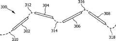
图1示出了根据现有技术的柔性电路类型的集成电路器件100的示意图。将示于图1中的细节程度大大减小以集中于这种器件的特征,这些特征在本发明的上下文中有关。FIG. 1 shows a schematic diagram of a flexible circuit type integrated
集成电路器件100含有衬底岛,这些衬底岛中的四个通过附图标记102、104、106和108示出。这些衬底岛含有电路块(未示出)。可在将硅晶片分成分离的衬底岛之前在硅晶片上用如公知的CMOS或BiCMOS处理技术制造这种衬底岛上的这些电路块。The
这些衬底岛具有相同的几何延伸件并且由可弹性变形的电桥连接,在图1中用大写字母A至K标记这些电桥。从下面的与根据本发明的集成电路器件200的比较会清楚地看出在无电桥的位置的大写字母L的使用,参看图2。含在各自的电桥中的信令层用导电材料制成并在图1中用Z字形线示意性地表示。这些信令层的布置用于指明各自的衬底岛上的电路块的位置,各自的信令层连接到该位置。例如,将衬底岛102和106连接的信令层110分别位于衬底岛102和106的各自的侧面102a和106a的中心略微靠左的位置。The substrate islands have the same geometric extension and are connected by elastically deformable bridges, which are marked with capital letters A to K in FIG. 1 . The use of the capital letter L at the bridge-free position will become clear from the following comparison with an
通过举例方式用附图标记110a和110b示出的点序列表示至衬底岛102和106上的各自的电路块的电气连接。The sequence of points shown by way of example with
信令层112至120具有小于其它电桥如电桥110的串联电阻,这种串联电阻由图1中用于信令层112至120的粗体印刷的各自的附图标记表示。因此,图1中的现有技术器件100使用至少两个不同类型的信令层。Signaling layers 112 to 120 have a smaller series resistance than other bridges, such as
出于例证目的在图1中示出了具有不同数量和类型的信令层的不同电桥A至K。本领域中熟练的技术人员会明白在该图和下面的图2中给出了根据现有技术(图1)和根据本发明(图2)的电桥设计规则而不是实际的器件结构。不同的示范性电桥构造提供相同的电气功能度,并且在两个视图中用大写字母A至L标记,以更容易地对不同的电桥设计进行比较。Different bridges A to K with different numbers and types of signaling layers are shown in FIG. 1 for illustration purposes. Those skilled in the art will appreciate that in this figure and in FIG. 2 below, bridge design rules according to the prior art (FIG. 1) and according to the present invention (FIG. 2) are given rather than actual device structures. The different exemplary bridge configurations provide the same electrical functionality and are labeled with capital letters A through L in both views for easier comparison of different bridge designs.
在集成电路器件100的电桥中的这些信令层通常含有高水平的机械应力,这些信令层如用钛(Ti)、氮化钛(TiN)或铜(Cu)制成。这种应力在制造过程中的热循环期间产生并由信令层与相邻的绝缘体之间的热膨胀系数(CTE)的失配所导致。可在形成集成电路器件100的柔性网中产生并不希望的不均匀应变分布,这些不均匀应力分布在最糟的情况下导致电桥A至K的破裂。These signaling layers in the bridges of the
图2示出了根据本发明的实施例的集成电路器件200的示意图。所示出的节段对应于示于图1中用于根据现有技术的集成电路器件100的节段,以允许对设计规则进行比较,这种比较由根据本发明的集成电路器件200实现。除了将第一个数字“1”用“2”替代之外,图2中的附图标记对应于图1中用于对应部分的附图标记。正如前面所提及的那样,在图2中也用大写字母A至L标记不同的电桥构造,以能够进行比较。FIG. 2 shows a schematic diagram of an
与根据现有技术的集成电路器件100相反,所有的电桥A至L含有相等数量的信号层,即四个信号层。同样也用之字形单线表示信号层。不过,通过引入虚设信令层在图2中进行进一步区分,这些虚设信令层用不间断的之字形线表示。例如,电桥E不仅含有对应于图1中的信令层110的已连接信令层210。电桥E还含有三个虚设信令层210a、210b和210c。In contrast to the
所示出的所有电桥构造具有四个信令层,这四个信令层电气连接或以虚设信令层的形式。不过,信令层的这种数量仅选择用于示范目的。通常希望提供具有最大可能数量的信令层的电桥以向单个衬底岛的电气连接电路块提供相互之间的最大柔性。All bridge configurations shown have four signaling layers which are electrically connected or in the form of dummy signaling layers. However, this number of signaling layers was chosen for exemplary purposes only. It is generally desirable to provide bridges with the largest possible number of signaling layers to provide maximum flexibility to each other for electrically connecting circuit blocks of a single substrate island.
集成电路器件200的电桥A至L还在几何层延伸件和不同的功能性层的材料方面具有相同的结构性设置。这样就可实现所有的电桥展示出相同的弹性模量值,而与它们在电气功能度方面的差异无关。这样就避免了由这些电桥中的内部应力所导致的在整个集成电路器件200的网中的并不希望的不均匀应变分布。The bridges A to L of the
因此,在这些电桥的设计中,机械性能尤其是提供相同的弹性模量值是优先设计约束条件。Therefore, in the design of these bridges, the mechanical properties especially providing the same elastic modulus values are the priority design constraints.
在这种设计约束条件下,可通过将电桥的两个或更多信令层并联来实现具有低串联电阻的连接。对信令层对212和220指明了这一点,该信令层对两个信令层,这两个信令层由这些衬底岛上的各自的金属节段成对并联。这样,电桥的结构就无需改变以在相邻的衬底岛上的不同电路块之间提供特别低的串联电阻。Within such design constraints, connections with low series resistance can be achieved by paralleling two or more signaling layers of the bridge. This is indicated for the pair of signaling
将现有技术的器件100中的电桥构造L与根据本发明的集成电路器件200中的电桥构造L进行比较也是有益的。在现有技术的器件中并不要求电气连接并因此而并不提供电桥,而图2中的集成电路器件200并不提供包括四个虚设信令层222a至222d的标准电桥。这样就避免了不同衬底岛的可弹性变形的连接中的不对称。同样,所希望的机械性能而不是所要求的电气功能度在电桥的设计中占有优势。It is also instructive to compare the bridge configuration L in the
在下面的表中,在以下范畴将现有技术的器件100中的电桥构造A至L与集成电路器件200(本发明)中的电桥构造A至L进行比较:信令层数量(对现有技术的器件和本发明的器件均适用)、低串联电阻层的数量(仅用在现有技术的器件中)、虚设信令层的数量(仅用在本发明的器件中)和(串联)连接的信令层的数量(仅用在本发明的器件中)。In the table below, bridge configurations A to L in

表1:图1和图2中的电桥构造比较Table 1: Comparison of Bridge Constructions in Figure 1 and Figure 2
前面的表表明现有技术的器件100的电桥设计受控于衬底岛之间的电气连通的要求。不过,在遵循本发明的设计规则时可实现相等的电气功能度,根据本发明的设计规则,向每个相邻的衬底岛提供电桥,并带有相等数量的信令层,这些信令层具有相等的几何延伸件和材料选择。这种设计实现用于电桥A至L中的每一个的相同的弹性模量,而提供相同的电气功能度作为图1的器件中的电桥构造A至L。The preceding table shows that the bridge design of the
在并不要求衬底岛之间的电气连接的情况下,使用仅含有虚设信令层的电桥。在将少于最大数量的信令层用在电桥中的情况下,通过适当的电气绝缘将未使用的信令层制成虚设信令层。在希望有具有特别低的串联电阻的信令层的情况下,将两个或更多的信令层并联。In cases where electrical connections between substrate islands are not required, bridges containing only dummy signaling layers are used. In case less than the maximum number of signaling layers are used in the bridge, the unused signaling layers are made as dummy signaling layers by suitable electrical insulation. In cases where signaling layers with particularly low series resistance are desired, two or more signaling layers are connected in parallel.
优选将这些电桥在每个衬底岛上的相等位置对称布置。这样就能够避免形成互连的衬底岛(如202和208)的网络的集成电路器件200中的不均匀应变分布。These bridges are preferably arranged symmetrically at equal locations on each substrate island. In this way, non-uniform strain distribution in
图3示出了本发明的集成电路器件的实施例的示意性侧视图。示于图3中的集成电路器件300包括衬底岛,这些衬底岛中的四个用附图标记302至308示出。所示出的这些衬底岛302至308是一种线性布置。部分,应理解图3也表示衬底岛的二维布置。Fig. 3 shows a schematic side view of an embodiment of an integrated circuit device of the present invention. The
这些衬底岛302至308通过可弹性变形的电桥310至318与它们各自的相邻衬底岛连接。这些电桥310至318用虚线示出。所示出的这些电桥310至318出于弯曲状态以表明它们的可变形性。这些电桥可弹性变形,且根据本发明,这些电桥均具有相同的或几乎相同的弹性模量值。These
图3示出了集成电路器件300所受到的弯曲完全由可弹性变形的电桥310至318所容纳。衬底岛302至308形成这种器件的刚性节段。应将衬底岛303至308的延伸件选择为大大小于弯曲半径,在工作条件下,电子电路器件300受到这种弯曲。这样,所有的应力会通过这些可弹性变形的电桥得到缓解。FIG. 3 shows that the bending experienced by the
正如将参考下面的视图所详细示出的那样,这些柔性电桥通常含有在这些衬底岛之间的电气互联。这些电桥通常会比这些衬底岛的延伸件短。不过,并不将这一点解释为一种限制。根据所希望的用途,这些电桥还可不这些衬底岛的延伸件长。下面将会示出一种实例。As will be shown in detail with reference to the following figures, the flex bridges typically contain electrical interconnections between the substrate islands. These bridges will generally be shorter than the extensions of the substrate islands. However, this is not to be construed as a limitation. Depending on the desired use, the bridges can also be longer than the extensions of the substrate islands. An example will be shown below.
注意,通常某些衬底岛会容纳某些功能。例如,一个或多个衬底岛可专用于提供存储能力。另一种衬底岛可含有锁相回路(PLL)电路。再一种衬底岛可含有处理器电路。衬底岛的专用功能度的另一种实例是模数(A/D)转换器电路。当然,根据衬底岛的大小,可将几个功能电路模块设在一个衬底岛上。衬底岛的通常的大小在毫米的范围内。不过,应根据特定用途的柔性要求选择大小。Note that generally certain substrate islands will accommodate certain functions. For example, one or more substrate islands may be dedicated to providing storage capabilities. Another type of substrate island may contain phase locked loop (PLL) circuitry. Yet another substrate island may contain processor circuitry. Another example of dedicated functionality for a substrate island is analog-to-digital (A/D) converter circuitry. Certainly, according to the size of the substrate island, several functional circuit modules can be arranged on one substrate island. Typical sizes of substrate islands are in the millimeter range. However, the size should be selected based on the flexibility required for a particular application.
还可使几个衬底岛与这些电桥一起共同执行单一功能,这些电桥的作用在于在这些衬底岛之间提供电气互联。例如,几个衬底岛可一起形成感应线圈。另一种实例是由衬底岛组形成天线,例如,以10×10矩阵布置这些衬底岛。可沿着这种矩阵的外衬底岛布置这种天线。这种矩阵本身可形成较大集成电路器件的区域。谐振电路的带宽通常足够大以容纳天线谐振频率的小偏差,这种偏差可由含有这种天线的衬底岛矩阵的变形所导致。It is also possible to have several substrate islands collectively performing a single function with these bridges whose role is to provide electrical interconnection between the substrate islands. For example, several substrate islands can together form an induction coil. Another example is to form an antenna from a group of substrate islands, for example, arranging the substrate islands in a 10x10 matrix. Such antennas may be arranged along the outer substrate islands of such a matrix. Such matrices can themselves form areas of larger integrated circuit devices. The bandwidth of the resonant circuit is usually large enough to accommodate small deviations in the resonant frequency of the antenna which may be caused by deformation of the matrix of substrate islands containing such an antenna.
下面将详细描述其它实施例和这些实施例的制造。Other embodiments and the manufacture of these embodiments will be described in detail below.
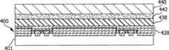
图4至图8示出了本发明的集成电路器件的实施例的生产期间的不同阶段。示于图4至图8中的截面是示意性截面。4 to 8 illustrate different stages during the production of an embodiment of an integrated circuit device of the present invention. The sections shown in FIGS. 4 to 8 are schematic sections.
图4示出了完全处理过的晶片400。晶片400是一种用如CMOS工艺设有电子电路的晶片。该实例利用标准的块状硅IC工艺,因此,采用块状硅衬底晶片401。不过,并不将这一点解释为一种限制。示于图4至图8中的还可与SOI晶片一起使用。在下面的描述中会明确地注意到,对于以SOI为基础的制造方法而言,与所描述的处理的偏差在何种情形中是必要的。FIG. 4 shows a fully processed
这种晶片含有衬底岛区域402和404,在随后的处理中,这些衬底岛区域将转变成单个的衬底岛。这些衬底岛区域含有有源电路元件406、408、410和412。将会理解,这些有源电路元件406至412表示任何适当的集成电路,可根据特定用途的需要设计这些集成电路。This wafer contains
在单个衬底岛区域402和404上的局部互连结构414至420在各自的衬底岛的集成电路内提供电信号传输。The
经过处理的晶片400还含有电桥区域422和424。这些电桥区域含有层序列,这种层序列由场效氧化物层426和典型的互连堆428形成,互连堆428含有电介质层(用与场效氧化物层426相同的影线示出)和金属互连430和432。这些金属互连在相邻的衬底岛之间提供信号传输。金属互连430和432分别含有水平互连节段430.1和432.1以及垂直互连节段430.2和432.2。水平互连节段430.1和432.1在电桥区域422和424中的互连堆428的顶部金属层内制造。而且,优选以弹簧形状的Z字形方式(在这些图中未示出)以垂直于所示出的截面的方向即平行于晶片表面的方向设计水平互连节段430.1和432.1的金属。
应理解晶片400继续向左而以相同的方式超过图4至图8所示。图4中的晶片400的右侧形成晶片边缘并因此而并不含有电桥区域。It should be understood that
正如可看出的那样,电桥区域430、432的结构相同。这样就可确保在随后的处理之后要形成的这些电桥也构造成具有相同的或几乎相同的弹性模量值。在电桥并不起到电气互联的作用的情形中,可将一个或多个垂直互连节段省略。这样就仅引入较少的结构修改,这种较少的结构修改对弹性模量在作用可忽略不计。As can be seen,
图5示出了处于随后的处理阶段的晶片400。已在此阶段将弹性聚合物层438应用于晶片400的互连堆428的表面。在该弹性聚合物层的顶部,通过粘合剂层442将玻璃支撑物440附到该衬底,在下面也将这种弹性聚合物层称为聚酰亚胺层438,且并无限制。Figure 5 shows the
在示于图6中的随后的处理阶段,已将硅衬底晶片401的厚度降低到约10μm,并将硅衬底晶片401蚀刻以形成衬底岛452和554。这些衬底岛由电桥区域422和424连接。In a subsequent processing stage shown in FIG. 6 , the
如图7所示,接着对这些电桥区域进行覆层各向异性干式蚀刻程序,这种程序将暴露的场效氧化物层426和层堆428的电介质层去除。合作制蚀刻在互连430.1和432.1的金属上停止。因此,这些互连起到硬蚀刻掩膜的作用。在这些互连的下面,在该干式蚀刻步骤之后留下薄的电介质层456,这种电介质层456将这些互连结合到聚酰亚胺层438。These bridge regions are then subjected to a blanket anisotropic dry etch process, which removes the exposed
在替代实施例中,通过各向异性蚀刻步骤的继续将剩余的电介质层456去除,这种各向异性蚀刻步骤可以是如一种湿式蚀刻步骤。这样,水平互连节段430.1和432.1就完全悬浮在空气中。不过,随后通常将该电路的两侧用聚酰亚胺(未示出)覆盖,聚酰亚胺会将这些互连包埋。In an alternative embodiment, the remaining
由于水平互连节段430.1和432.1呈之字形,而且由于下层聚酰亚胺层438的原因,这些电桥会起到弹簧的作用,在施加机械应力期间,这些弹簧具有相同的弹性模量。这一点与仅剩余非常少的电介质(通常是陶瓷)材料的情况相结合会避免电桥432和434在施加机械应力期间破裂。Due to the zigzag shape of the horizontal interconnection segments 430.1 and 432.1 and due to the
在最后的步骤中将玻璃支撑物440和粘合剂层442去除,该最后步骤的结果在图8中示出。The
图9和图10示出了根据本发明的另一个实施例的集成电路器件的制造过程中的两个阶段。用于本实施例的处理通常与示于图4至图8中的处理类似。9 and 10 illustrate two stages in the fabrication process of an integrated circuit device according to another embodiment of the present invention. The processing for this embodiment is generally similar to that shown in FIGS. 4-8.
图9表示与图4中的处理节段对应的处理阶段。示于图9中的晶片900与示于图4中的晶片400的不同之处在于金属互联结构930和932具有也以垂直于该晶片表面的方向的之字形。这通过使这些金属互连的水平节段在相邻的互连层之间交替来实现,从而实现最小的可能节距。FIG. 9 shows processing stages corresponding to the processing segments in FIG. 4 .
图10示出了对应于图4至图8的实施例的处理之后的处理过的晶片。示于图10中的最后处理阶段对应于图8中的处理阶段。FIG. 10 shows the processed wafer after processing corresponding to the embodiment of FIGS. 4-8 . The final processing stage shown in FIG. 10 corresponds to the processing stage in FIG. 8 .
图11至图13示出了本发明的集成电路器件的另一个实施例的生产期间的不同阶段。用类似于对图4至图8所描述的方式对晶片1100进行处理。不过,下面将专注于与前面所描述的处理相比的较少差异。在本实施例中,在对应于示于图4中的晶片400的晶片结构的晶片结构1100的基础上,上金属层面1102并不是由标准的层间电介质材料覆盖,而是由弹性聚合物层1104覆盖。在通过粘合剂层1110将支撑物1108附到该晶片之前将中间剥离层1106淀积在弹性层1104上。例如,这种剥离层可以是一种二氧化硅层,但也可选择适用于剥离工艺的另一种材料。11 to 13 illustrate different stages during the production of another embodiment of an integrated circuit device of the present invention.
接着对这种硅衬底像前面参考图7所描述的那样进行处理。之后应用弹性聚合物层1112以包埋这些电路岛,在本图中用附图标记1114和1116示出这些电路岛,参看图12。之后通过剥离工艺将玻璃支撑物1108去除,这种剥离工艺选择性地去除二氧化硅层1106以及二氧化硅层1106所具有的粘合剂1110和支撑物1108,并留下完成的集成电路器件完全嵌入弹性材料中。This silicon substrate is then processed as previously described with reference to FIG. 7 . A layer of
弹性聚合物层在整个器件的均匀应用确保能够使衬底岛1114与1116之间的这些电桥1118的弹性模量相同。The uniform application of the elastic polymer layer throughout the device ensures that the modulus of elasticity of the
虽然用于弹性聚合物层1104和1112的优选材料是聚酰亚胺,但也有聚酰亚胺树脂的替代材料选择,如聚酰胺-酰亚胺(polyamide-imide)、聚醚-酰亚胺、聚硅氧烷-酰亚胺、聚醚-酮树脂和本领域中公知的类似材料。所选择的材料的弹性性能为各向同性是重要的,以确保以二维类似于矩阵的器件的所有方向的电桥的相同的弹性模量。While the preferred material for the
在下面的权利要求书中,附图标记不应解释为对权利要求书的范围进行限制。In the following claims, reference signs shall not be construed as limiting the scope of the claims.
Claims (23)
Applications Claiming Priority (2)
| Application Number | Priority Date | Filing Date | Title |
|---|---|---|---|
| EP06112384.0 | 2006-04-07 | ||
| EP06112384 | 2006-04-07 |
Publications (1)
| Publication Number | Publication Date |
|---|---|
| CN101416302Atrue CN101416302A (en) | 2009-04-22 |
Family
ID=38420545
Family Applications (1)
| Application Number | Title | Priority Date | Filing Date |
|---|---|---|---|
| CNA200780012607XAPendingCN101416302A (en) | 2006-04-07 | 2007-04-03 | Elastically deformable integrated circuit devices |
Country Status (7)
| Country | Link |
|---|---|
| US (1) | US20090283891A1 (en) |
| EP (1) | EP2008303B1 (en) |
| JP (1) | JP2009533839A (en) |
| CN (1) | CN101416302A (en) |
| AT (1) | ATE471572T1 (en) |
| DE (1) | DE602007007201D1 (en) |
| WO (1) | WO2007116344A1 (en) |
Cited By (10)
| Publication number | Priority date | Publication date | Assignee | Title |
|---|---|---|---|---|
| CN102809373A (en)* | 2011-05-31 | 2012-12-05 | 精工爱普生株式会社 | Module and electronic apparatus |
| CN104347591A (en)* | 2014-09-10 | 2015-02-11 | 朱慧珑 | Flexible integrated circuit device, and subassembly and manufacturing method of flexible integrated circuit device |
| US9052220B2 (en) | 2011-05-31 | 2015-06-09 | Seiko Epson Corporation | Maintaining member, module, and electronic apparatus |
| US9243909B2 (en) | 2011-05-31 | 2016-01-26 | Seiko Epson Corporation | Module and electronic apparatus |
| CN105580207A (en)* | 2013-05-14 | 2016-05-11 | Mc10股份有限公司 | Conformal electronics including nested serpentine interconnects |
| CN107431059A (en)* | 2015-01-02 | 2017-12-01 | 亚利桑那州立大学董事会 | Archimedes spiral for deformable electronic installation designs |
| CN109704268A (en)* | 2019-02-21 | 2019-05-03 | 厦门大学 | A Stretchable Electron Interference Deformation Immune Substrate |
| CN109817687A (en)* | 2019-02-15 | 2019-05-28 | 京东方科技集团股份有限公司 | A flexible substrate and OLED display panel |
| CN109951946A (en)* | 2013-02-25 | 2019-06-28 | Mc10股份有限公司 | Structure is alleviated in strain for stretchable interconnection piece |
| CN111009562A (en)* | 2018-10-08 | 2020-04-14 | 乐金显示有限公司 | Stretchable display panel and device and method for manufacturing stretchable display device |
Families Citing this family (65)
| Publication number | Priority date | Publication date | Assignee | Title |
|---|---|---|---|---|
| US7834424B2 (en)* | 2006-09-12 | 2010-11-16 | The Board Of Trustees Of The Leland Stanford Junior University | Extendable connector and network |
| FR2917895B1 (en)* | 2007-06-21 | 2010-04-09 | Commissariat Energie Atomique | METHOD FOR MANUFACTURING AN ASSEMBLY OF MECHANICALLY CONNECTED CHIPS USING A FLEXIBLE CONNECTION |
| TWI723953B (en) | 2008-03-05 | 2021-04-11 | 美國伊利諾大學理事會 | Stretchable and foldable electronic devices |
| JP5646492B2 (en)* | 2008-10-07 | 2014-12-24 | エムシー10 インコーポレイテッドMc10,Inc. | Stretchable integrated circuit and device with sensor array |
| US8389862B2 (en) | 2008-10-07 | 2013-03-05 | Mc10, Inc. | Extremely stretchable electronics |
| US9123614B2 (en) | 2008-10-07 | 2015-09-01 | Mc10, Inc. | Methods and applications of non-planar imaging arrays |
| US8097926B2 (en) | 2008-10-07 | 2012-01-17 | Mc10, Inc. | Systems, methods, and devices having stretchable integrated circuitry for sensing and delivering therapy |
| EP2356680B1 (en)* | 2008-11-12 | 2015-04-08 | Mc10, Inc. | Extremely stretchable electronics |
| CA2780747C (en)* | 2008-11-12 | 2020-08-25 | Mc10, Inc. | Extremely stretchable electronics |
| EP2386117A4 (en)* | 2009-01-12 | 2017-12-27 | Mc10, Inc. | Methods and applications of non-planar imaging arrays |
| PL2392196T3 (en) | 2009-01-30 | 2019-05-31 | Imec Vzw | Stretchable electronic device |
| WO2010102310A2 (en)* | 2009-03-03 | 2010-09-10 | Mc10, Inc. | Systems, methods, and devices having stretchable integrated circuitry for sensing and delivering therapy |
| US8344955B2 (en) | 2010-01-08 | 2013-01-01 | Nokia Corporation | Integrated antenna with e-flex technology |
| JP5560738B2 (en)* | 2010-02-01 | 2014-07-30 | 日本電気株式会社 | Semiconductor device, three-dimensional integrated circuit and manufacturing method thereof |
| EP2355144A1 (en) | 2010-02-09 | 2011-08-10 | Nederlandse Organisatie voor toegepast -natuurwetenschappelijk onderzoek TNO | Component placement on flexible and/or stretchable substrates |
| WO2011143300A1 (en)* | 2010-05-12 | 2011-11-17 | Monolithe Semiconductor Inc. | Extendable network structure |
| US8987913B2 (en) | 2010-05-12 | 2015-03-24 | Monolithe Semiconductor Inc. | Deformable network structure |
| US8716603B2 (en) | 2010-11-24 | 2014-05-06 | Nokia Corporation | Printed wiring board with dielectric material sections having different dissipation factors |
| EP2461658A1 (en) | 2010-12-03 | 2012-06-06 | Nederlandse Organisatie voor toegepast -natuurwetenschappelijk onderzoek TNO | Method and apparatus for assembling electric components on a flexible substrate as well as assembly of an electric component with a flexible substrate |
| US20120279762A1 (en)* | 2011-05-03 | 2012-11-08 | Industry-Academic Cooperation Foundation, Yonsei University | Composition for forming stretchable conductive pattern, method of producing the stretchable conductive pattern using the composition, and electronic device including stretchable conductive electrode |
| JP5741306B2 (en)* | 2011-08-10 | 2015-07-01 | 富士通株式会社 | Electronic device and manufacturing method thereof |
| EP2675253A1 (en)* | 2012-06-15 | 2013-12-18 | BIOTRONIK SE & Co. KG | Flexible-rigid circuit board composite and method for producing a flexible-rigid circuit board composite |
| US9168094B2 (en) | 2012-07-05 | 2015-10-27 | Mc10, Inc. | Catheter device including flow sensing |
| US9295842B2 (en) | 2012-07-05 | 2016-03-29 | Mc10, Inc. | Catheter or guidewire device including flow sensing and use thereof |
| JP2014048090A (en)* | 2012-08-30 | 2014-03-17 | Seiko Epson Corp | Electronic module, electronic apparatus, and movable body |
| WO2014058473A1 (en) | 2012-10-09 | 2014-04-17 | Mc10, Inc. | Conformal electronics integrated with apparel |
| US9171794B2 (en) | 2012-10-09 | 2015-10-27 | Mc10, Inc. | Embedding thin chips in polymer |
| JP5583815B1 (en)* | 2013-04-22 | 2014-09-03 | 株式会社フジクラ | Multilayer wiring board and manufacturing method thereof |
| US8927338B1 (en) | 2013-06-13 | 2015-01-06 | International Business Machines Corporation | Flexible, stretchable electronic devices |
| JP6002322B2 (en)* | 2013-06-19 | 2016-10-05 | 株式会社フジクラ | Stretchable substrate, circuit board, and method for manufacturing stretchable substrate |
| CA2920485A1 (en) | 2013-08-05 | 2015-02-12 | Mc10, Inc. | Flexible temperature sensor including conformable electronics |
| KR20160065948A (en) | 2013-10-07 | 2016-06-09 | 엠씨10, 인크 | Conformal sensor systems for sensing and analysis |
| EP3071096A4 (en) | 2013-11-22 | 2017-08-09 | Mc10, Inc. | Conformal sensor systems for sensing and analysis of cardiac activity |
| US10153519B2 (en) | 2013-12-27 | 2018-12-11 | Arizona Board Of Regents On Behalf Of Arizona State University | Deformable origami batteries |
| CN105874606B (en) | 2014-01-06 | 2021-01-12 | Mc10股份有限公司 | Encapsulated conformal electronic systems and devices and methods of making and using the same |
| US10485118B2 (en) | 2014-03-04 | 2019-11-19 | Mc10, Inc. | Multi-part flexible encapsulation housing for electronic devices and methods of making the same |
| EP2991460B1 (en)* | 2014-08-29 | 2018-11-21 | Nokia Technologies OY | An apparatus and associated methods for deformable electronics |
| WO2016049444A1 (en) | 2014-09-26 | 2016-03-31 | Arizona Board Of Regents On Behalf Of Arizona State University | Stretchable batteries |
| US9899330B2 (en) | 2014-10-03 | 2018-02-20 | Mc10, Inc. | Flexible electronic circuits with embedded integrated circuit die |
| US10297572B2 (en)* | 2014-10-06 | 2019-05-21 | Mc10, Inc. | Discrete flexible interconnects for modules of integrated circuits |
| USD781270S1 (en) | 2014-10-15 | 2017-03-14 | Mc10, Inc. | Electronic device having antenna |
| US10502991B2 (en) | 2015-02-05 | 2019-12-10 | The Arizona Board Of Regents On Behalf Of Arizona State University | Origami displays and methods for their manufacture |
| WO2016134306A1 (en) | 2015-02-20 | 2016-08-25 | Mc10, Inc. | Automated detection and configuration of wearable devices based on on-body status, location, and/or orientation |
| WO2016140961A1 (en) | 2015-03-02 | 2016-09-09 | Mc10, Inc. | Perspiration sensor |
| JP2016178121A (en) | 2015-03-18 | 2016-10-06 | タツタ電線株式会社 | Stretchable cable and stretchable circuit board |
| WO2017015000A1 (en)* | 2015-07-17 | 2017-01-26 | Mc10, Inc. | Conductive stiffener, method of making a conductive stiffener, and conductive adhesive and encapsulation layers |
| US10709384B2 (en) | 2015-08-19 | 2020-07-14 | Mc10, Inc. | Wearable heat flux devices and methods of use |
| EP4079383A3 (en) | 2015-10-01 | 2023-02-22 | Medidata Solutions, Inc. | Method and system for interacting with a virtual environment |
| US10532211B2 (en) | 2015-10-05 | 2020-01-14 | Mc10, Inc. | Method and system for neuromodulation and stimulation |
| US20170181276A1 (en)* | 2015-12-21 | 2017-06-22 | Panasonic Intellectual Property Management Co., Ltd. | Substrate including stretchable sheet |
| US10277386B2 (en) | 2016-02-22 | 2019-04-30 | Mc10, Inc. | System, devices, and method for on-body data and power transmission |
| US10673280B2 (en) | 2016-02-22 | 2020-06-02 | Mc10, Inc. | System, device, and method for coupled hub and sensor node on-body acquisition of sensor information |
| CN109310340A (en) | 2016-04-19 | 2019-02-05 | Mc10股份有限公司 | Method and system for measuring sweat |
| US10390698B2 (en) | 2016-06-16 | 2019-08-27 | Arizona Board Of Regents On Behalf Of Arizona State University | Conductive and stretchable polymer composite |
| DE102016212129B4 (en)* | 2016-07-04 | 2022-05-19 | Schweizer Electronic Ag | Radio frequency transmission/reception element and method of manufacturing a radio frequency transmission/reception element |
| JP6781983B2 (en)* | 2016-08-05 | 2020-11-11 | 国立研究開発法人産業技術総合研究所 | Electronic devices and their manufacturing methods |
| US10447347B2 (en) | 2016-08-12 | 2019-10-15 | Mc10, Inc. | Wireless charger and high speed data off-loader |
| JP6972523B2 (en)* | 2016-09-13 | 2021-11-24 | セイコーエプソン株式会社 | Electronics |
| CN106455303B (en)* | 2016-11-15 | 2019-02-05 | 中国科学院力学研究所 | A kind of extensible inkjet printing flexible circuit board and preparation method thereof |
| CN209265885U (en)* | 2018-09-19 | 2019-08-16 | 昆山工研院新型平板显示技术中心有限公司 | Stretch electrode and the electronic device comprising it |
| CN110649181B (en)* | 2019-10-08 | 2022-04-26 | 京东方科技集团股份有限公司 | Display substrate, display device, and preparation method of display substrate |
| US11260705B2 (en) | 2019-12-17 | 2022-03-01 | The Goodyear Tire & Rubber Company | Flexible tire sensor unit |
| CN111462637B (en)* | 2020-05-29 | 2022-07-01 | 上海天马微电子有限公司 | Display panel and display device |
| KR20230164976A (en)* | 2022-05-26 | 2023-12-05 | 한국전자통신연구원 | Stretchable electronic device |
| KR102721872B1 (en) | 2022-11-30 | 2024-10-25 | 한국과학기술연구원 | Auxetic stretchable substrate with flexible joint structure and method for manufacturing the same |
Family Cites Families (21)
| Publication number | Priority date | Publication date | Assignee | Title |
|---|---|---|---|---|
| US3519890A (en)* | 1968-04-01 | 1970-07-07 | North American Rockwell | Low stress lead |
| US4754544A (en)* | 1985-01-30 | 1988-07-05 | Energy Conversion Devices, Inc. | Extremely lightweight, flexible semiconductor device arrays |
| JP2763445B2 (en)* | 1992-04-03 | 1998-06-11 | 三菱電機株式会社 | High frequency signal wiring and bonding device therefor |
| JPH0636620A (en)* | 1992-07-14 | 1994-02-10 | Nec Gumma Ltd | Flexible flat cable |
| JPH0997870A (en)* | 1995-09-29 | 1997-04-08 | S I I R D Center:Kk | Electronic device and its manufacture |
| US6027958A (en)* | 1996-07-11 | 2000-02-22 | Kopin Corporation | Transferred flexible integrated circuit |
| KR100476524B1 (en)* | 1997-12-31 | 2005-08-29 | 삼성전자주식회사 | Tape Carrier Package for LCD Module |
| DE59803887D1 (en)* | 1998-01-22 | 2002-05-23 | Fraunhofer Ges Forschung | MICROSYSTEM AND METHOD FOR PRODUCING A MICROSYSTEM |
| US6617671B1 (en)* | 1999-06-10 | 2003-09-09 | Micron Technology, Inc. | High density stackable and flexible substrate-based semiconductor device modules |
| US6743982B2 (en)* | 2000-11-29 | 2004-06-01 | Xerox Corporation | Stretchable interconnects using stress gradient films |
| DE10122324A1 (en)* | 2001-05-08 | 2002-11-14 | Philips Corp Intellectual Pty | Flexible integrated monolithic circuit |
| US6455931B1 (en)* | 2001-05-15 | 2002-09-24 | Raytheon Company | Monolithic microelectronic array structure having substrate islands and its fabrication |
| US6627865B1 (en)* | 2001-05-15 | 2003-09-30 | Raytheon Company | Nonplanar integrated optical device array structure and a method for its fabrication |
| AU2002330718A1 (en)* | 2001-09-03 | 2003-03-18 | National Microelectronic Research Centre University College Cork - National University Of Ireland Co | Integrated circuit structure and a method of making an integrated circuit structure |
| US7011530B2 (en)* | 2002-05-24 | 2006-03-14 | Sitaraman Suresh K | Multi-axis compliance spring |
| JP3670636B2 (en)* | 2002-10-09 | 2005-07-13 | 株式会社日立製作所 | Electronic device with electronic components mounted |
| US6872589B2 (en)* | 2003-02-06 | 2005-03-29 | Kulicke & Soffa Investments, Inc. | High density chip level package for the packaging of integrated circuits and method to manufacture same |
| US7491892B2 (en)* | 2003-03-28 | 2009-02-17 | Princeton University | Stretchable and elastic interconnects |
| JP4291209B2 (en)* | 2004-05-20 | 2009-07-08 | エルピーダメモリ株式会社 | Manufacturing method of semiconductor device |
| US7629691B2 (en)* | 2004-06-16 | 2009-12-08 | Honeywell International Inc. | Conductor geometry for electronic circuits fabricated on flexible substrates |
| JP2006108431A (en)* | 2004-10-06 | 2006-04-20 | Sharp Corp | Semiconductor device |
- 2007
- 2007-04-03CNCNA200780012607XApatent/CN101416302A/enactivePending
- 2007-04-03DEDE602007007201Tpatent/DE602007007201D1/enactiveActive
- 2007-04-03USUS12/295,782patent/US20090283891A1/ennot_activeAbandoned
- 2007-04-03JPJP2009503711Apatent/JP2009533839A/ennot_activeCeased
- 2007-04-03ATAT07735369Tpatent/ATE471572T1/ennot_activeIP Right Cessation
- 2007-04-03WOPCT/IB2007/051190patent/WO2007116344A1/enactiveApplication Filing
- 2007-04-03EPEP07735369Apatent/EP2008303B1/ennot_activeNot-in-force
Cited By (20)
| Publication number | Priority date | Publication date | Assignee | Title |
|---|---|---|---|---|
| US10113875B2 (en) | 2011-05-31 | 2018-10-30 | Seiko Epson Corporation | Module and electronic apparatus |
| US9052220B2 (en) | 2011-05-31 | 2015-06-09 | Seiko Epson Corporation | Maintaining member, module, and electronic apparatus |
| US9243909B2 (en) | 2011-05-31 | 2016-01-26 | Seiko Epson Corporation | Module and electronic apparatus |
| CN102809373B (en)* | 2011-05-31 | 2016-02-17 | 精工爱普生株式会社 | Module and electronic equipment |
| US9316499B2 (en) | 2011-05-31 | 2016-04-19 | Seiko Epson Corporation | Module and electronic apparatus |
| CN102809373A (en)* | 2011-05-31 | 2012-12-05 | 精工爱普生株式会社 | Module and electronic apparatus |
| US10072954B2 (en) | 2011-05-31 | 2018-09-11 | Seiko Epson Corporation | Module and electronic apparatus |
| CN109951946B (en)* | 2013-02-25 | 2021-10-01 | 美谛达解决方案公司 | Strain relief structures for stretchable interconnects |
| CN109951946A (en)* | 2013-02-25 | 2019-06-28 | Mc10股份有限公司 | Structure is alleviated in strain for stretchable interconnection piece |
| CN105580207B (en)* | 2013-05-14 | 2019-03-12 | Mc10股份有限公司 | Conformal electronics including nested serpentine interconnects |
| CN105580207A (en)* | 2013-05-14 | 2016-05-11 | Mc10股份有限公司 | Conformal electronics including nested serpentine interconnects |
| CN104347591A (en)* | 2014-09-10 | 2015-02-11 | 朱慧珑 | Flexible integrated circuit device, and subassembly and manufacturing method of flexible integrated circuit device |
| CN107431059A (en)* | 2015-01-02 | 2017-12-01 | 亚利桑那州立大学董事会 | Archimedes spiral for deformable electronic installation designs |
| CN107431059B (en)* | 2015-01-02 | 2020-03-17 | 亚利桑那州立大学董事会 | Archimedes spiral design for deformable electronics |
| CN111009562A (en)* | 2018-10-08 | 2020-04-14 | 乐金显示有限公司 | Stretchable display panel and device and method for manufacturing stretchable display device |
| CN111009562B (en)* | 2018-10-08 | 2023-09-15 | 乐金显示有限公司 | Stretchable display panel and device and manufacturing method of stretchable display device |
| US12033544B2 (en) | 2018-10-08 | 2024-07-09 | Lg Display Co., Ltd. | Stretchable display panel and device and manufacturing method of the same |
| CN109817687A (en)* | 2019-02-15 | 2019-05-28 | 京东方科技集团股份有限公司 | A flexible substrate and OLED display panel |
| CN109817687B (en)* | 2019-02-15 | 2021-10-08 | 京东方科技集团股份有限公司 | Flexible substrate and OLED display panel |
| CN109704268A (en)* | 2019-02-21 | 2019-05-03 | 厦门大学 | A Stretchable Electron Interference Deformation Immune Substrate |
Also Published As
| Publication number | Publication date |
|---|---|
| JP2009533839A (en) | 2009-09-17 |
| ATE471572T1 (en) | 2010-07-15 |
| DE602007007201D1 (en) | 2010-07-29 |
| US20090283891A1 (en) | 2009-11-19 |
| EP2008303B1 (en) | 2010-06-16 |
| EP2008303A1 (en) | 2008-12-31 |
| WO2007116344A1 (en) | 2007-10-18 |
Similar Documents
| Publication | Publication Date | Title |
|---|---|---|
| CN101416302A (en) | Elastically deformable integrated circuit devices | |
| US10383219B2 (en) | Extremely stretchable electronics | |
| EP2902293B1 (en) | Methods of making extremely stretchable electronics | |
| JP3359910B2 (en) | Microsystem and method of manufacturing microsystem | |
| US10679946B2 (en) | Methods and devices for solderless integration of multiple semiconductor dies on flexible substrates | |
| US20130287935A1 (en) | Method of fabricating of circuit board | |
| EP2902294B1 (en) | Extremely stretchable electronics | |
| KR100809284B1 (en) | Tactile sensor array and manufacturing method | |
| KR101680443B1 (en) | Stretchable substrates with locally varied stiffness and stretchable electronics packages produced using the same substrates and Producing Method Thereof | |
| CN101820721B (en) | Substrate for circuit board, circuit board and method for manufacturing circuit board | |
| HK1161421B (en) | Extremely stretchable electronics | |
| HK1159848B (en) | Stretchable and foldable electronic devices |
Legal Events
| Date | Code | Title | Description |
|---|---|---|---|
| C06 | Publication | ||
| PB01 | Publication | ||
| C10 | Entry into substantive examination | ||
| SE01 | Entry into force of request for substantive examination | ||
| C02 | Deemed withdrawal of patent application after publication (patent law 2001) | ||
| WD01 | Invention patent application deemed withdrawn after publication | Open date:20090422 |