CN101416293B - Method to improve the step coverage and pattern loading for dielectric films - Google Patents
Method to improve the step coverage and pattern loading for dielectric filmsDownload PDFInfo
- Publication number
- CN101416293B CN101416293BCN2007800121574ACN200780012157ACN101416293BCN 101416293 BCN101416293 BCN 101416293BCN 2007800121574 ACN2007800121574 ACN 2007800121574ACN 200780012157 ACN200780012157 ACN 200780012157ACN 101416293 BCN101416293 BCN 101416293B
- Authority
- CN
- China
- Prior art keywords
- silicon
- plasma
- dielectric layer
- film
- layer
- Prior art date
- Legal status (The legal status is an assumption and is not a legal conclusion. Google has not performed a legal analysis and makes no representation as to the accuracy of the status listed.)
- Expired - Fee Related
Links
- 238000000034methodMethods0.000titleclaimsabstractdescription81
- 239000000758substrateSubstances0.000claimsabstractdescription76
- 238000000151depositionMethods0.000claimsabstractdescription66
- 239000007789gasSubstances0.000claimsabstractdescription63
- XUIMIQQOPSSXEZ-UHFFFAOYSA-NSiliconChemical compound[Si]XUIMIQQOPSSXEZ-UHFFFAOYSA-N0.000claimsabstractdescription62
- QVGXLLKOCUKJST-UHFFFAOYSA-Natomic oxygenChemical compound[O]QVGXLLKOCUKJST-UHFFFAOYSA-N0.000claimsabstractdescription61
- 229910052760oxygenInorganic materials0.000claimsabstractdescription61
- 239000001301oxygenSubstances0.000claimsabstractdescription61
- 239000010703siliconSubstances0.000claimsabstractdescription61
- 229910052710siliconInorganic materials0.000claimsabstractdescription61
- 239000002243precursorSubstances0.000claimsabstractdescription57
- 238000005530etchingMethods0.000claimsabstractdescription39
- 229910052736halogenInorganic materials0.000claimsabstractdescription15
- 150000002367halogensChemical class0.000claimsabstractdescription15
- 238000006243chemical reactionMethods0.000claimsdescription94
- HMMGMWAXVFQUOA-UHFFFAOYSA-NoctamethylcyclotetrasiloxaneChemical compoundC[Si]1(C)O[Si](C)(C)O[Si](C)(C)O[Si](C)(C)O1HMMGMWAXVFQUOA-UHFFFAOYSA-N0.000claimsdescription32
- IJGRMHOSHXDMSA-UHFFFAOYSA-NAtomic nitrogenChemical compoundN#NIJGRMHOSHXDMSA-UHFFFAOYSA-N0.000claimsdescription23
- GQPLMRYTRLFLPF-UHFFFAOYSA-NNitrous OxideChemical compound[O-][N+]#NGQPLMRYTRLFLPF-UHFFFAOYSA-N0.000claimsdescription23
- 229910052581Si3N4Inorganic materials0.000claimsdescription21
- HQVNEWCFYHHQES-UHFFFAOYSA-Nsilicon nitrideChemical groupN12[Si]34N5[Si]62N3[Si]51N64HQVNEWCFYHHQES-UHFFFAOYSA-N0.000claimsdescription21
- 125000002496methyl groupChemical group[H]C([H])([H])*0.000claimsdescription11
- 229910052757nitrogenInorganic materials0.000claimsdescription11
- VYPSYNLAJGMNEJ-UHFFFAOYSA-NSilicium dioxideChemical groupO=[Si]=OVYPSYNLAJGMNEJ-UHFFFAOYSA-N0.000claimsdescription10
- 239000001272nitrous oxideSubstances0.000claimsdescription10
- 229910052814silicon oxideInorganic materials0.000claimsdescription10
- 229910052731fluorineInorganic materials0.000claimsdescription8
- 239000011737fluorineSubstances0.000claimsdescription8
- QKCGXXHCELUCKW-UHFFFAOYSA-Nn-[4-[4-(dinaphthalen-2-ylamino)phenyl]phenyl]-n-naphthalen-2-ylnaphthalen-2-amineChemical compoundC1=CC=CC2=CC(N(C=3C=CC(=CC=3)C=3C=CC(=CC=3)N(C=3C=C4C=CC=CC4=CC=3)C=3C=C4C=CC=CC4=CC=3)C3=CC4=CC=CC=C4C=C3)=CC=C21QKCGXXHCELUCKW-UHFFFAOYSA-N0.000claimsdescription8
- 238000010926purgeMethods0.000claimsdescription7
- 125000006850spacer groupChemical group0.000claimsdescription7
- WKBOTKDWSSQWDR-UHFFFAOYSA-NBromine atomChemical compound[Br]WKBOTKDWSSQWDR-UHFFFAOYSA-N0.000claimsdescription6
- ZAMOUSCENKQFHK-UHFFFAOYSA-NChlorine atomChemical compound[Cl]ZAMOUSCENKQFHK-UHFFFAOYSA-N0.000claimsdescription6
- BLRPTPMANUNPDV-UHFFFAOYSA-NSilaneChemical compound[SiH4]BLRPTPMANUNPDV-UHFFFAOYSA-N0.000claimsdescription6
- GDTBXPJZTBHREO-UHFFFAOYSA-NbromineSubstancesBrBrGDTBXPJZTBHREO-UHFFFAOYSA-N0.000claimsdescription6
- 229910052794bromiumInorganic materials0.000claimsdescription6
- 239000000460chlorineSubstances0.000claimsdescription6
- 229910052801chlorineInorganic materials0.000claimsdescription6
- 229910000077silaneInorganic materials0.000claimsdescription6
- VXEGSRKPIUDPQT-UHFFFAOYSA-N4-[4-(4-methoxyphenyl)piperazin-1-yl]anilineChemical compoundC1=CC(OC)=CC=C1N1CCN(C=2C=CC(N)=CC=2)CC1VXEGSRKPIUDPQT-UHFFFAOYSA-N0.000claimsdescription5
- VJIYRPVGAZXYBD-UHFFFAOYSA-NdibromosilaneChemical compoundBr[SiH2]BrVJIYRPVGAZXYBD-UHFFFAOYSA-N0.000claimsdescription5
- GAURFLBIDLSLQU-UHFFFAOYSA-Ndiethoxy(methyl)siliconChemical compoundCCO[Si](C)OCCGAURFLBIDLSLQU-UHFFFAOYSA-N0.000claimsdescription5
- AIFMYMZGQVTROK-UHFFFAOYSA-Nsilicon tetrabromideChemical compoundBr[Si](Br)(Br)BrAIFMYMZGQVTROK-UHFFFAOYSA-N0.000claimsdescription5
- 239000005049silicon tetrachlorideSubstances0.000claimsdescription5
- ZDHXKXAHOVTTAH-UHFFFAOYSA-NtrichlorosilaneChemical compoundCl[SiH](Cl)ClZDHXKXAHOVTTAH-UHFFFAOYSA-N0.000claimsdescription5
- 239000005052trichlorosilaneSubstances0.000claimsdescription5
- MROCJMGDEKINLD-UHFFFAOYSA-NdichlorosilaneChemical compoundCl[SiH2]ClMROCJMGDEKINLD-UHFFFAOYSA-N0.000claimsdescription4
- PZPGRFITIJYNEJ-UHFFFAOYSA-NdisilaneChemical compound[SiH3][SiH3]PZPGRFITIJYNEJ-UHFFFAOYSA-N0.000claimsdescription4
- 125000002887hydroxy groupChemical group[H]O*0.000claimsdescription4
- QJGQUHMNIGDVPM-UHFFFAOYSA-Nnitrogen groupChemical group[N]QJGQUHMNIGDVPM-UHFFFAOYSA-N0.000claimsdescription4
- 125000000217alkyl groupChemical group0.000claimsdescription3
- VYIRVGYSUZPNLF-UHFFFAOYSA-Nn-(tert-butylamino)silyl-2-methylpropan-2-amineChemical compoundCC(C)(C)N[SiH2]NC(C)(C)CVYIRVGYSUZPNLF-UHFFFAOYSA-N0.000claimsdescription3
- UMVBXBACMIOFDO-UHFFFAOYSA-N[N].[Si]Chemical compound[N].[Si]UMVBXBACMIOFDO-UHFFFAOYSA-N0.000claimsdescription2
- GVGCUCJTUSOZKP-UHFFFAOYSA-Nnitrogen trifluorideChemical compoundFN(F)FGVGCUCJTUSOZKP-UHFFFAOYSA-N0.000claimsdescription2
- 238000012546transferMethods0.000claimsdescription2
- PXGOKWXKJXAPGV-UHFFFAOYSA-NFluorineChemical compoundFFPXGOKWXKJXAPGV-UHFFFAOYSA-N0.000claims1
- 230000008021depositionEffects0.000abstractdescription46
- 150000002500ionsChemical class0.000abstractdescription2
- 239000010410layerSubstances0.000description171
- 239000010408filmSubstances0.000description89
- 210000002381plasmaAnatomy0.000description65
- 230000000694effectsEffects0.000description25
- 238000005137deposition processMethods0.000description23
- 238000009832plasma treatmentMethods0.000description19
- XKRFYHLGVUSROY-UHFFFAOYSA-NArgonChemical compound[Ar]XKRFYHLGVUSROY-UHFFFAOYSA-N0.000description18
- 238000012545processingMethods0.000description18
- 238000000623plasma-assisted chemical vapour depositionMethods0.000description15
- 239000001307heliumSubstances0.000description14
- 229910052734heliumInorganic materials0.000description14
- SWQJXJOGLNCZEY-UHFFFAOYSA-Nhelium atomChemical compound[He]SWQJXJOGLNCZEY-UHFFFAOYSA-N0.000description14
- 238000010586diagramMethods0.000description11
- 229910052786argonInorganic materials0.000description9
- 238000011282treatmentMethods0.000description8
- QGZKDVFQNNGYKY-UHFFFAOYSA-NAmmoniaChemical compoundNQGZKDVFQNNGYKY-UHFFFAOYSA-N0.000description7
- YCKRFDGAMUMZLT-UHFFFAOYSA-NFluorine atomChemical compound[F]YCKRFDGAMUMZLT-UHFFFAOYSA-N0.000description7
- 238000005229chemical vapour depositionMethods0.000description7
- OKTJSMMVPCPJKN-UHFFFAOYSA-NCarbonChemical compound[C]OKTJSMMVPCPJKN-UHFFFAOYSA-N0.000description6
- 229910052799carbonInorganic materials0.000description6
- 239000000463materialSubstances0.000description6
- 239000004065semiconductorSubstances0.000description6
- 230000004888barrier functionEffects0.000description5
- 238000011065in-situ storageMethods0.000description5
- 238000001020plasma etchingMethods0.000description4
- 229910021529ammoniaInorganic materials0.000description3
- 239000012159carrier gasSubstances0.000description3
- 238000004140cleaningMethods0.000description3
- 239000003989dielectric materialSubstances0.000description3
- 239000011261inert gasSubstances0.000description3
- 229910052582BNInorganic materials0.000description2
- PZNSFCLAULLKQX-UHFFFAOYSA-NBoron nitrideChemical compoundN#BPZNSFCLAULLKQX-UHFFFAOYSA-N0.000description2
- -1MDEOS)Chemical compound0.000description2
- 238000000231atomic layer depositionMethods0.000description2
- 230000008901benefitEffects0.000description2
- 239000003085diluting agentSubstances0.000description2
- 238000010849ion bombardmentMethods0.000description2
- 238000004518low pressure chemical vapour depositionMethods0.000description2
- 238000004519manufacturing processMethods0.000description2
- 238000005259measurementMethods0.000description2
- 239000002052molecular layerSubstances0.000description2
- 150000004767nitridesChemical class0.000description2
- 230000006911nucleationEffects0.000description2
- 238000010899nucleationMethods0.000description2
- 238000003672processing methodMethods0.000description2
- 238000009738saturatingMethods0.000description2
- 238000001878scanning electron micrographMethods0.000description2
- 238000000926separation methodMethods0.000description2
- HBMJWWWQQXIZIP-UHFFFAOYSA-Nsilicon carbideChemical compound[Si+]#[C-]HBMJWWWQQXIZIP-UHFFFAOYSA-N0.000description2
- 238000012360testing methodMethods0.000description2
- 239000010409thin filmSubstances0.000description2
- 102100022717Atypical chemokine receptor 1Human genes0.000description1
- FNNNDGRSNHMVSM-UHFFFAOYSA-NC(C)(C)(C)N[SiH2]NC(C)(C)C.C(C)(C)(C)N[SiH2]NC(C)(C)CChemical compoundC(C)(C)(C)N[SiH2]NC(C)(C)C.C(C)(C)(C)N[SiH2]NC(C)(C)CFNNNDGRSNHMVSM-UHFFFAOYSA-N0.000description1
- 101000678879Homo sapiens Atypical chemokine receptor 1Proteins0.000description1
- 229910008051Si-OHInorganic materials0.000description1
- 229910006358Si—OHInorganic materials0.000description1
- BOTDANWDWHJENH-UHFFFAOYSA-NTetraethyl orthosilicateChemical compoundCCO[Si](OCC)(OCC)OCCBOTDANWDWHJENH-UHFFFAOYSA-N0.000description1
- PPWPWBNSKBDSPK-UHFFFAOYSA-N[B].[C]Chemical compound[B].[C]PPWPWBNSKBDSPK-UHFFFAOYSA-N0.000description1
- CFOAUMXQOCBWNJ-UHFFFAOYSA-N[B].[Si]Chemical compound[B].[Si]CFOAUMXQOCBWNJ-UHFFFAOYSA-N0.000description1
- ZILJFRYKLPPLTO-UHFFFAOYSA-N[C].[B].[Si]Chemical compound[C].[B].[Si]ZILJFRYKLPPLTO-UHFFFAOYSA-N0.000description1
- PRPAGESBURMWTI-UHFFFAOYSA-N[C].[F]Chemical compound[C].[F]PRPAGESBURMWTI-UHFFFAOYSA-N0.000description1
- OBNDGIHQAIXEAO-UHFFFAOYSA-N[O].[Si]Chemical compound[O].[Si]OBNDGIHQAIXEAO-UHFFFAOYSA-N0.000description1
- 230000002411adverseEffects0.000description1
- 230000015572biosynthetic processEffects0.000description1
- 238000007664blowingMethods0.000description1
- 235000008429breadNutrition0.000description1
- 239000002131composite materialSubstances0.000description1
- 230000007423decreaseEffects0.000description1
- 230000007547defectEffects0.000description1
- LBVWYGNGGJURHQ-UHFFFAOYSA-NdicarbonChemical compound[C-]#[C+]LBVWYGNGGJURHQ-UHFFFAOYSA-N0.000description1
- AWFPGKLDLMAPMK-UHFFFAOYSA-NdimethylaminosiliconChemical compoundCN(C)[Si]AWFPGKLDLMAPMK-UHFFFAOYSA-N0.000description1
- 229910001873dinitrogenInorganic materials0.000description1
- 238000009826distributionMethods0.000description1
- 238000002474experimental methodMethods0.000description1
- 239000001257hydrogenSubstances0.000description1
- 229910052739hydrogenInorganic materials0.000description1
- 125000004435hydrogen atomChemical class[H]*0.000description1
- 239000011229interlayerSubstances0.000description1
- 238000001000micrographMethods0.000description1
- 235000013842nitrous oxideNutrition0.000description1
- 230000001590oxidative effectEffects0.000description1
- 239000003642reactive oxygen metaboliteSubstances0.000description1
- 238000004626scanning electron microscopyMethods0.000description1
- 238000007789sealingMethods0.000description1
- 229910021332silicideInorganic materials0.000description1
- 229910010271silicon carbideInorganic materials0.000description1
- LIVNPJMFVYWSIS-UHFFFAOYSA-Nsilicon monoxideChemical compound[Si-]#[O+]LIVNPJMFVYWSIS-UHFFFAOYSA-N0.000description1
- 239000002210silicon-based materialSubstances0.000description1
- 239000000126substanceSubstances0.000description1
- TXEYQDLBPFQVAA-UHFFFAOYSA-NtetrafluoromethaneChemical compoundFC(F)(F)FTXEYQDLBPFQVAA-UHFFFAOYSA-N0.000description1
Images


Classifications
- C—CHEMISTRY; METALLURGY
- C23—COATING METALLIC MATERIAL; COATING MATERIAL WITH METALLIC MATERIAL; CHEMICAL SURFACE TREATMENT; DIFFUSION TREATMENT OF METALLIC MATERIAL; COATING BY VACUUM EVAPORATION, BY SPUTTERING, BY ION IMPLANTATION OR BY CHEMICAL VAPOUR DEPOSITION, IN GENERAL; INHIBITING CORROSION OF METALLIC MATERIAL OR INCRUSTATION IN GENERAL
- C23C—COATING METALLIC MATERIAL; COATING MATERIAL WITH METALLIC MATERIAL; SURFACE TREATMENT OF METALLIC MATERIAL BY DIFFUSION INTO THE SURFACE, BY CHEMICAL CONVERSION OR SUBSTITUTION; COATING BY VACUUM EVAPORATION, BY SPUTTERING, BY ION IMPLANTATION OR BY CHEMICAL VAPOUR DEPOSITION, IN GENERAL
- C23C16/00—Chemical coating by decomposition of gaseous compounds, without leaving reaction products of surface material in the coating, i.e. chemical vapour deposition [CVD] processes
- C23C16/04—Coating on selected surface areas, e.g. using masks
- C23C16/045—Coating cavities or hollow spaces, e.g. interior of tubes; Infiltration of porous substrates
- C—CHEMISTRY; METALLURGY
- C23—COATING METALLIC MATERIAL; COATING MATERIAL WITH METALLIC MATERIAL; CHEMICAL SURFACE TREATMENT; DIFFUSION TREATMENT OF METALLIC MATERIAL; COATING BY VACUUM EVAPORATION, BY SPUTTERING, BY ION IMPLANTATION OR BY CHEMICAL VAPOUR DEPOSITION, IN GENERAL; INHIBITING CORROSION OF METALLIC MATERIAL OR INCRUSTATION IN GENERAL
- C23C—COATING METALLIC MATERIAL; COATING MATERIAL WITH METALLIC MATERIAL; SURFACE TREATMENT OF METALLIC MATERIAL BY DIFFUSION INTO THE SURFACE, BY CHEMICAL CONVERSION OR SUBSTITUTION; COATING BY VACUUM EVAPORATION, BY SPUTTERING, BY ION IMPLANTATION OR BY CHEMICAL VAPOUR DEPOSITION, IN GENERAL
- C23C16/00—Chemical coating by decomposition of gaseous compounds, without leaving reaction products of surface material in the coating, i.e. chemical vapour deposition [CVD] processes
- C23C16/22—Chemical coating by decomposition of gaseous compounds, without leaving reaction products of surface material in the coating, i.e. chemical vapour deposition [CVD] processes characterised by the deposition of inorganic material, other than metallic material
- C23C16/30—Deposition of compounds, mixtures or solid solutions, e.g. borides, carbides, nitrides
- C23C16/40—Oxides
- C23C16/401—Oxides containing silicon
- C—CHEMISTRY; METALLURGY
- C23—COATING METALLIC MATERIAL; COATING MATERIAL WITH METALLIC MATERIAL; CHEMICAL SURFACE TREATMENT; DIFFUSION TREATMENT OF METALLIC MATERIAL; COATING BY VACUUM EVAPORATION, BY SPUTTERING, BY ION IMPLANTATION OR BY CHEMICAL VAPOUR DEPOSITION, IN GENERAL; INHIBITING CORROSION OF METALLIC MATERIAL OR INCRUSTATION IN GENERAL
- C23C—COATING METALLIC MATERIAL; COATING MATERIAL WITH METALLIC MATERIAL; SURFACE TREATMENT OF METALLIC MATERIAL BY DIFFUSION INTO THE SURFACE, BY CHEMICAL CONVERSION OR SUBSTITUTION; COATING BY VACUUM EVAPORATION, BY SPUTTERING, BY ION IMPLANTATION OR BY CHEMICAL VAPOUR DEPOSITION, IN GENERAL
- C23C16/00—Chemical coating by decomposition of gaseous compounds, without leaving reaction products of surface material in the coating, i.e. chemical vapour deposition [CVD] processes
- C23C16/56—After-treatment
- H—ELECTRICITY
- H01—ELECTRIC ELEMENTS
- H01L—SEMICONDUCTOR DEVICES NOT COVERED BY CLASS H10
- H01L21/00—Processes or apparatus adapted for the manufacture or treatment of semiconductor or solid state devices or of parts thereof
- H01L21/02—Manufacture or treatment of semiconductor devices or of parts thereof
- H01L21/02104—Forming layers
- H01L21/02107—Forming insulating materials on a substrate
- H01L21/02109—Forming insulating materials on a substrate characterised by the type of layer, e.g. type of material, porous/non-porous, pre-cursors, mixtures or laminates
- H01L21/02112—Forming insulating materials on a substrate characterised by the type of layer, e.g. type of material, porous/non-porous, pre-cursors, mixtures or laminates characterised by the material of the layer
- H01L21/02123—Forming insulating materials on a substrate characterised by the type of layer, e.g. type of material, porous/non-porous, pre-cursors, mixtures or laminates characterised by the material of the layer the material containing silicon
- H01L21/02126—Forming insulating materials on a substrate characterised by the type of layer, e.g. type of material, porous/non-porous, pre-cursors, mixtures or laminates characterised by the material of the layer the material containing silicon the material containing Si, O, and at least one of H, N, C, F, or other non-metal elements, e.g. SiOC, SiOC:H or SiONC
- H—ELECTRICITY
- H01—ELECTRIC ELEMENTS
- H01L—SEMICONDUCTOR DEVICES NOT COVERED BY CLASS H10
- H01L21/00—Processes or apparatus adapted for the manufacture or treatment of semiconductor or solid state devices or of parts thereof
- H01L21/02—Manufacture or treatment of semiconductor devices or of parts thereof
- H01L21/02104—Forming layers
- H01L21/02107—Forming insulating materials on a substrate
- H01L21/02109—Forming insulating materials on a substrate characterised by the type of layer, e.g. type of material, porous/non-porous, pre-cursors, mixtures or laminates
- H01L21/02112—Forming insulating materials on a substrate characterised by the type of layer, e.g. type of material, porous/non-porous, pre-cursors, mixtures or laminates characterised by the material of the layer
- H01L21/02123—Forming insulating materials on a substrate characterised by the type of layer, e.g. type of material, porous/non-porous, pre-cursors, mixtures or laminates characterised by the material of the layer the material containing silicon
- H01L21/02164—Forming insulating materials on a substrate characterised by the type of layer, e.g. type of material, porous/non-porous, pre-cursors, mixtures or laminates characterised by the material of the layer the material containing silicon the material being a silicon oxide, e.g. SiO2
- H—ELECTRICITY
- H01—ELECTRIC ELEMENTS
- H01L—SEMICONDUCTOR DEVICES NOT COVERED BY CLASS H10
- H01L21/00—Processes or apparatus adapted for the manufacture or treatment of semiconductor or solid state devices or of parts thereof
- H01L21/02—Manufacture or treatment of semiconductor devices or of parts thereof
- H01L21/02104—Forming layers
- H01L21/02107—Forming insulating materials on a substrate
- H01L21/02109—Forming insulating materials on a substrate characterised by the type of layer, e.g. type of material, porous/non-porous, pre-cursors, mixtures or laminates
- H01L21/02112—Forming insulating materials on a substrate characterised by the type of layer, e.g. type of material, porous/non-porous, pre-cursors, mixtures or laminates characterised by the material of the layer
- H01L21/02123—Forming insulating materials on a substrate characterised by the type of layer, e.g. type of material, porous/non-porous, pre-cursors, mixtures or laminates characterised by the material of the layer the material containing silicon
- H01L21/0217—Forming insulating materials on a substrate characterised by the type of layer, e.g. type of material, porous/non-porous, pre-cursors, mixtures or laminates characterised by the material of the layer the material containing silicon the material being a silicon nitride not containing oxygen, e.g. SixNy or SixByNz
- H—ELECTRICITY
- H01—ELECTRIC ELEMENTS
- H01L—SEMICONDUCTOR DEVICES NOT COVERED BY CLASS H10
- H01L21/00—Processes or apparatus adapted for the manufacture or treatment of semiconductor or solid state devices or of parts thereof
- H01L21/02—Manufacture or treatment of semiconductor devices or of parts thereof
- H01L21/02104—Forming layers
- H01L21/02107—Forming insulating materials on a substrate
- H01L21/02109—Forming insulating materials on a substrate characterised by the type of layer, e.g. type of material, porous/non-porous, pre-cursors, mixtures or laminates
- H01L21/02205—Forming insulating materials on a substrate characterised by the type of layer, e.g. type of material, porous/non-porous, pre-cursors, mixtures or laminates the layer being characterised by the precursor material for deposition
- H01L21/02208—Forming insulating materials on a substrate characterised by the type of layer, e.g. type of material, porous/non-porous, pre-cursors, mixtures or laminates the layer being characterised by the precursor material for deposition the precursor containing a compound comprising Si
- H01L21/02211—Forming insulating materials on a substrate characterised by the type of layer, e.g. type of material, porous/non-porous, pre-cursors, mixtures or laminates the layer being characterised by the precursor material for deposition the precursor containing a compound comprising Si the compound being a silane, e.g. disilane, methylsilane or chlorosilane
- H—ELECTRICITY
- H01—ELECTRIC ELEMENTS
- H01L—SEMICONDUCTOR DEVICES NOT COVERED BY CLASS H10
- H01L21/00—Processes or apparatus adapted for the manufacture or treatment of semiconductor or solid state devices or of parts thereof
- H01L21/02—Manufacture or treatment of semiconductor devices or of parts thereof
- H01L21/02104—Forming layers
- H01L21/02107—Forming insulating materials on a substrate
- H01L21/02109—Forming insulating materials on a substrate characterised by the type of layer, e.g. type of material, porous/non-porous, pre-cursors, mixtures or laminates
- H01L21/02205—Forming insulating materials on a substrate characterised by the type of layer, e.g. type of material, porous/non-porous, pre-cursors, mixtures or laminates the layer being characterised by the precursor material for deposition
- H01L21/02208—Forming insulating materials on a substrate characterised by the type of layer, e.g. type of material, porous/non-porous, pre-cursors, mixtures or laminates the layer being characterised by the precursor material for deposition the precursor containing a compound comprising Si
- H01L21/02214—Forming insulating materials on a substrate characterised by the type of layer, e.g. type of material, porous/non-porous, pre-cursors, mixtures or laminates the layer being characterised by the precursor material for deposition the precursor containing a compound comprising Si the compound comprising silicon and oxygen
- H01L21/02216—Forming insulating materials on a substrate characterised by the type of layer, e.g. type of material, porous/non-porous, pre-cursors, mixtures or laminates the layer being characterised by the precursor material for deposition the precursor containing a compound comprising Si the compound comprising silicon and oxygen the compound being a molecule comprising at least one silicon-oxygen bond and the compound having hydrogen or an organic group attached to the silicon or oxygen, e.g. a siloxane
- H—ELECTRICITY
- H01—ELECTRIC ELEMENTS
- H01L—SEMICONDUCTOR DEVICES NOT COVERED BY CLASS H10
- H01L21/00—Processes or apparatus adapted for the manufacture or treatment of semiconductor or solid state devices or of parts thereof
- H01L21/02—Manufacture or treatment of semiconductor devices or of parts thereof
- H01L21/02104—Forming layers
- H01L21/02107—Forming insulating materials on a substrate
- H01L21/02225—Forming insulating materials on a substrate characterised by the process for the formation of the insulating layer
- H01L21/0226—Forming insulating materials on a substrate characterised by the process for the formation of the insulating layer formation by a deposition process
- H01L21/02263—Forming insulating materials on a substrate characterised by the process for the formation of the insulating layer formation by a deposition process deposition from the gas or vapour phase
- H01L21/02271—Forming insulating materials on a substrate characterised by the process for the formation of the insulating layer formation by a deposition process deposition from the gas or vapour phase deposition by decomposition or reaction of gaseous or vapour phase compounds, i.e. chemical vapour deposition
- H01L21/02274—Forming insulating materials on a substrate characterised by the process for the formation of the insulating layer formation by a deposition process deposition from the gas or vapour phase deposition by decomposition or reaction of gaseous or vapour phase compounds, i.e. chemical vapour deposition in the presence of a plasma [PECVD]
- H—ELECTRICITY
- H01—ELECTRIC ELEMENTS
- H01L—SEMICONDUCTOR DEVICES NOT COVERED BY CLASS H10
- H01L21/00—Processes or apparatus adapted for the manufacture or treatment of semiconductor or solid state devices or of parts thereof
- H01L21/02—Manufacture or treatment of semiconductor devices or of parts thereof
- H01L21/02104—Forming layers
- H01L21/02365—Forming inorganic semiconducting materials on a substrate
- H01L21/02612—Formation types
- H01L21/02617—Deposition types
- H01L21/0262—Reduction or decomposition of gaseous compounds, e.g. CVD
- H—ELECTRICITY
- H01—ELECTRIC ELEMENTS
- H01L—SEMICONDUCTOR DEVICES NOT COVERED BY CLASS H10
- H01L21/00—Processes or apparatus adapted for the manufacture or treatment of semiconductor or solid state devices or of parts thereof
- H01L21/02—Manufacture or treatment of semiconductor devices or of parts thereof
- H01L21/04—Manufacture or treatment of semiconductor devices or of parts thereof the devices having potential barriers, e.g. a PN junction, depletion layer or carrier concentration layer
- H01L21/18—Manufacture or treatment of semiconductor devices or of parts thereof the devices having potential barriers, e.g. a PN junction, depletion layer or carrier concentration layer the devices having semiconductor bodies comprising elements of Group IV of the Periodic Table or AIIIBV compounds with or without impurities, e.g. doping materials
- H01L21/30—Treatment of semiconductor bodies using processes or apparatus not provided for in groups H01L21/20 - H01L21/26
- H01L21/31—Treatment of semiconductor bodies using processes or apparatus not provided for in groups H01L21/20 - H01L21/26 to form insulating layers thereon, e.g. for masking or by using photolithographic techniques; After treatment of these layers; Selection of materials for these layers
- H01L21/3105—After-treatment
- H01L21/311—Etching the insulating layers by chemical or physical means
- H01L21/31105—Etching inorganic layers
- H01L21/31111—Etching inorganic layers by chemical means
- H01L21/31116—Etching inorganic layers by chemical means by dry-etching
- H—ELECTRICITY
- H01—ELECTRIC ELEMENTS
- H01L—SEMICONDUCTOR DEVICES NOT COVERED BY CLASS H10
- H01L21/00—Processes or apparatus adapted for the manufacture or treatment of semiconductor or solid state devices or of parts thereof
- H01L21/70—Manufacture or treatment of devices consisting of a plurality of solid state components formed in or on a common substrate or of parts thereof; Manufacture of integrated circuit devices or of parts thereof
- H01L21/71—Manufacture of specific parts of devices defined in group H01L21/70
- H01L21/768—Applying interconnections to be used for carrying current between separate components within a device comprising conductors and dielectrics
- H01L21/76801—Applying interconnections to be used for carrying current between separate components within a device comprising conductors and dielectrics characterised by the formation and the after-treatment of the dielectrics, e.g. smoothing
- H01L21/76822—Modification of the material of dielectric layers, e.g. grading, after-treatment to improve the stability of the layers, to increase their density etc.
- H01L21/76826—Modification of the material of dielectric layers, e.g. grading, after-treatment to improve the stability of the layers, to increase their density etc. by contacting the layer with gases, liquids or plasmas
- H—ELECTRICITY
- H01—ELECTRIC ELEMENTS
- H01L—SEMICONDUCTOR DEVICES NOT COVERED BY CLASS H10
- H01L21/00—Processes or apparatus adapted for the manufacture or treatment of semiconductor or solid state devices or of parts thereof
- H01L21/70—Manufacture or treatment of devices consisting of a plurality of solid state components formed in or on a common substrate or of parts thereof; Manufacture of integrated circuit devices or of parts thereof
- H01L21/71—Manufacture of specific parts of devices defined in group H01L21/70
- H01L21/768—Applying interconnections to be used for carrying current between separate components within a device comprising conductors and dielectrics
- H01L21/76801—Applying interconnections to be used for carrying current between separate components within a device comprising conductors and dielectrics characterised by the formation and the after-treatment of the dielectrics, e.g. smoothing
- H01L21/76829—Applying interconnections to be used for carrying current between separate components within a device comprising conductors and dielectrics characterised by the formation and the after-treatment of the dielectrics, e.g. smoothing characterised by the formation of thin functional dielectric layers, e.g. dielectric etch-stop, barrier, capping or liner layers
- H01L21/76834—Applying interconnections to be used for carrying current between separate components within a device comprising conductors and dielectrics characterised by the formation and the after-treatment of the dielectrics, e.g. smoothing characterised by the formation of thin functional dielectric layers, e.g. dielectric etch-stop, barrier, capping or liner layers formation of thin insulating films on the sidewalls or on top of conductors
- H—ELECTRICITY
- H01—ELECTRIC ELEMENTS
- H01L—SEMICONDUCTOR DEVICES NOT COVERED BY CLASS H10
- H01L21/00—Processes or apparatus adapted for the manufacture or treatment of semiconductor or solid state devices or of parts thereof
- H01L21/02—Manufacture or treatment of semiconductor devices or of parts thereof
- H01L21/02104—Forming layers
- H01L21/02107—Forming insulating materials on a substrate
- H01L21/02225—Forming insulating materials on a substrate characterised by the process for the formation of the insulating layer
- H01L21/0226—Forming insulating materials on a substrate characterised by the process for the formation of the insulating layer formation by a deposition process
- H01L21/02263—Forming insulating materials on a substrate characterised by the process for the formation of the insulating layer formation by a deposition process deposition from the gas or vapour phase
- H01L21/02271—Forming insulating materials on a substrate characterised by the process for the formation of the insulating layer formation by a deposition process deposition from the gas or vapour phase deposition by decomposition or reaction of gaseous or vapour phase compounds, i.e. chemical vapour deposition
- H01L21/0228—Forming insulating materials on a substrate characterised by the process for the formation of the insulating layer formation by a deposition process deposition from the gas or vapour phase deposition by decomposition or reaction of gaseous or vapour phase compounds, i.e. chemical vapour deposition deposition by cyclic CVD, e.g. ALD, ALE, pulsed CVD
Landscapes
- Engineering & Computer Science (AREA)
- Chemical & Material Sciences (AREA)
- Physics & Mathematics (AREA)
- Power Engineering (AREA)
- Condensed Matter Physics & Semiconductors (AREA)
- General Physics & Mathematics (AREA)
- Manufacturing & Machinery (AREA)
- Computer Hardware Design (AREA)
- Microelectronics & Electronic Packaging (AREA)
- Chemical Kinetics & Catalysis (AREA)
- General Chemical & Material Sciences (AREA)
- Mechanical Engineering (AREA)
- Metallurgy (AREA)
- Organic Chemistry (AREA)
- Materials Engineering (AREA)
- Inorganic Chemistry (AREA)
- Plasma & Fusion (AREA)
- Spectroscopy & Molecular Physics (AREA)
- Formation Of Insulating Films (AREA)
- Chemical Vapour Deposition (AREA)
- Internal Circuitry In Semiconductor Integrated Circuit Devices (AREA)
- Drying Of Semiconductors (AREA)
Abstract
Translated fromChinese
Description
Translated fromChinese技术领域technical field
本发明的实施例大致上有关于半导体处理的方法及设备。更明确而言,本发明实施例是有关于沉积共形介电膜层的方法及设备。Embodiments of the invention generally relate to methods and apparatus for semiconductor processing. More specifically, embodiments of the present invention relate to methods and apparatus for depositing conformal dielectric films.
背景技术Background technique
通过数种气体的化学反应在一基板上形成介电层是当代半导体器件制造过程的主要步骤中的其中一个步骤。这些沉积处理包含化学气相沉积(CVD)与等离子体增强式化学气相沉积(PECVD),其中等离子体增强化学气相沉积是结合等离子体与传统CVD技术的沉积处理。The formation of a dielectric layer on a substrate by the chemical reaction of several gases is one of the major steps in the fabrication process of contemporary semiconductor devices. These deposition processes include chemical vapor deposition (CVD) and plasma enhanced chemical vapor deposition (PECVD), wherein plasma enhanced chemical vapor deposition is a deposition process that combines plasma and conventional CVD techniques.
CVD以及PECVD介电层可做为半导体器件中的不同膜层。例如,这些介电层可以做为器件中导线或互连之间的层间介电层。或者,这些介电层可做为阻障层、蚀刻终止层或间隙壁以及其它膜层。CVD and PECVD dielectric layers can be used as different layers in semiconductor devices. For example, these dielectric layers can act as interlayer dielectrics between wires or interconnects in a device. Alternatively, these dielectric layers may serve as barrier layers, etch stop layers or spacers, among other layers.
用来做为阻障层与间隙壁的介电层通常沉积在图案化的基板中的特征上,例如沉积在用来形成后续线路的水平互连、垂直互连(通孔)、栅极堆栈层等特征上。较佳者,沉积处理提供一共形膜层(conformal layer)。然而,共形沉积通常是难以达成的。Dielectric layers used as barriers and spacers are usually deposited on features in the patterned substrate, such as horizontal interconnects, vertical interconnects (vias), gate stacks used to form subsequent circuits layers and other features. Preferably, the deposition process provides a conformal layer. However, conformal deposition is often difficult to achieve.
举例而言,将阻障层沉积在特征上时很难不产生表面缺陷或特征变形等情形。在沉积的过程中,阻障层材料可能形成凸块(overloaf),也就是在通孔的肩部沉积过多材料却在通孔的底部沉积过少材料,而形成看起来像是面包侧边的凸块状造型。此种现象也因为该通孔底部的轮廓看起来像脚而被称为底脚现象(footing)。在极端的例子里,通孔的肩部会合拢而在通孔的顶部形成一接合密封表面。当整个晶片上的膜层厚度不均匀时,可能会对每个装置的驱动电流性质造成不良影响。仅仅调整处理参数并无法显著地改善阶梯覆盖与图案加载的问题。For example, it is difficult to deposit a barrier layer on a feature without creating surface defects or deformation of the feature. During deposition, the barrier layer material can form an overloaf, that is, deposit too much material on the shoulder of the via and deposit too little material on the bottom of the via, forming what looks like the side of a bread bump shape. This phenomenon is also called footing because the contour of the bottom of the via looks like a foot. In extreme cases, the shoulders of the through-holes may converge to form a joint sealing surface at the top of the through-hole. When the film thickness is not uniform across the wafer, it can adversely affect the drive current properties of each device. Just adjusting the processing parameters cannot significantly improve the problem of ladder coverage and pattern loading.
在栅极堆栈层上沉积将于后续用来形成间隙壁的共形膜层亦是一种挑战。虽然目前已发展出使用传统高温低压CVD来沉积作为间隙壁的氮化硅与氧化硅层的方法,然而此类技术的热预算过高而可能使半导体器件的几何形状持续收缩。虽然氮化硅的PECVD处理可以在较低的温度下执行,然而所得到的阶梯覆盖与图案加载结果却无法如利用高温低压CVD方法所形成的结果般地令人满意。Depositing a conformal layer on the gate stack layer that will later be used to form spacers is also a challenge. Although conventional high temperature and low pressure CVD methods have been developed to deposit silicon nitride and silicon oxide layers as spacers, the thermal budget of such techniques is too high and may continue to shrink the geometry of semiconductor devices. Although PECVD of silicon nitride can be performed at lower temperatures, the obtained step coverage and pattern loading results are not as satisfactory as those formed by using high temperature and low pressure CVD methods.
因此,目前需要一种能在图案化基板中已形成的特征上沉积共形膜层的方法。Accordingly, there is a need for a method of depositing conformal layers on features already formed in a patterned substrate.
发明内容Contents of the invention
本发明实施例提供一种在基板上形成介电膜层的方法,该方法包括如下步骤:将一表面上具有至少一个已形成的特征的基板放置于一反应室中;沉积一介电层;用等离子体处理该介电层;测定该介电层的厚度;以及重复执行上述沉积介电层的步骤,用等离子体处理该介电层并判断该介电层厚度。An embodiment of the present invention provides a method for forming a dielectric film layer on a substrate, the method comprising the following steps: placing a substrate having at least one formed feature on a surface in a reaction chamber; depositing a dielectric layer; Treating the dielectric layer with plasma; measuring the thickness of the dielectric layer; and repeating the steps of depositing the dielectric layer, treating the dielectric layer with plasma and judging the thickness of the dielectric layer.
在一实施例中,提供一种于一反应室内在一图案化基板上形成一膜层的方法。该方法包括使该图案化基板在存在有一等离子体的情况下暴露于一含硅的前驱物中(例如八甲基环四硅氧烷,octamethylcyclotetrasiloxane)以在该图案化基板上沉积一膜层,以及待沉积该膜层后,利用由诸如氧气等含氧气体所形成的等离子体来处理该膜层。重复执行该暴露步骤与处理步骤直到获得所期望的膜层厚度为止。该膜层可能是一氧化硅层或是一掺杂碳的氧化硅层。In one embodiment, a method for forming a film layer on a patterned substrate in a reaction chamber is provided. The method includes exposing the patterned substrate to a silicon-containing precursor (eg, octamethylcyclotetrasiloxane) in the presence of a plasma to deposit a film on the patterned substrate, And after the film layer is deposited, the film layer is treated with a plasma formed by an oxygen-containing gas such as oxygen. The exposing and processing steps are repeated until the desired film thickness is obtained. The film layer may be a silicon oxide layer or a carbon-doped silicon oxide layer.
在另一实施例中,于一反应室内在一图案化基板上形成一膜层的方法包括使该图案化基板在存在有一等离子体的情况下暴露于一含硅前驱物中以在该图案化基板上沉积一膜层,以及待沉积该膜层后,利用由一含氮气体所形成的等离子体来处理该膜层,以及重复该暴露步骤与处理步骤直到获得所期望的膜层厚度为止。In another embodiment, a method of forming a layer on a patterned substrate in a chamber includes exposing the patterned substrate to a silicon-containing precursor in the presence of a plasma to A film is deposited on the substrate, and after the film is deposited, the film is treated with plasma formed by a nitrogen-containing gas, and the exposing and processing steps are repeated until the desired film thickness is obtained.
本发明实施例亦提供一种控制基板上膜层的阶梯覆盖与图案加载的方法。在一实施例中,该方法包括将基板表面上具有至少一个已形成特征的基板放置于一反应室中;一介电层沉积在该基板上,并使用由含氧或含卤素气体所形成的等离子体来蚀刻该介电层,以在该至少一个已形成的特征上提供具有所期望轮廓的介电层,其中该含卤素气体选自于由氟、氯、溴及其组合所构成的群组中。The embodiment of the present invention also provides a method for controlling step coverage and pattern loading of a film layer on a substrate. In one embodiment, the method includes placing a substrate having at least one formed feature on a surface of the substrate in a reaction chamber; depositing a dielectric layer on the substrate and using a plasma to etch the dielectric layer to provide a dielectric layer with a desired profile on the at least one formed feature, wherein the halogen-containing gas is selected from the group consisting of fluorine, chlorine, bromine, and combinations thereof group.
在另一实施例中,该方法包括将一基板表面上具有至少一个已形成特征的基板放置于一反应室中,以及沉积一介电层在该基板上。该特征包含一顶面、一侧面以及一底面。该介电层沉积在顶面上的厚度比其沉积在底面与侧面上的厚度要厚。随后利用由含氧或含卤素气体所形成的等离子体来蚀刻该介电层,其中该含卤素气体选自于由氟、氯、溴及其组合物所构成的群组中。该介电层顶面上的蚀刻速率高于该介电层底面及侧面上的蚀刻速率。执行一次或多次的介电层沉积与蚀刻步骤,以在该至少一个已形成特征上提供具有所期望轮廓的介电层。In another embodiment, the method includes placing a substrate having at least one formed feature on a surface of the substrate in a reaction chamber, and depositing a dielectric layer on the substrate. The feature includes a top surface, a side surface and a bottom surface. The dielectric layer is deposited thicker on the top surface than on the bottom and side surfaces. The dielectric layer is then etched using a plasma formed from an oxygen-containing or halogen-containing gas selected from the group consisting of fluorine, chlorine, bromine, and combinations thereof. The etch rate on the top surface of the dielectric layer is higher than the etch rate on the bottom surface and sides of the dielectric layer. One or more dielectric layer deposition and etching steps are performed to provide a dielectric layer having a desired profile on the at least one formed feature.
在更进一步的实施例中,该方法包括将一基板表面上具有至少一个已形成特征的基板放置于一反应室中,以及沉积一氮化硅介电层在该基板上。该特征包含一顶面、一侧面与一底面。该氮化硅介电层沉积在顶面上的厚度比其沉积在底面与侧面上的厚度要厚。随后利用三氟化氮(NF3)等离子体蚀刻该介电层,并且该NF3等离子体在顶面上的蚀刻速率高于其在底面及侧面上的蚀刻速率,以在该至少一个已形成特征上提供具有所期望轮廓的氮化硅介电层。可执行一次或多次的氮化硅介电层沉积与蚀刻步骤,以提供所期望的轮廓。In still further embodiments, the method includes placing a substrate having at least one formed feature on a surface of the substrate in a reaction chamber, and depositing a silicon nitride dielectric layer on the substrate. The feature includes a top surface, a side surface and a bottom surface. The silicon nitride dielectric layer is deposited thicker on the top surface than on the bottom and side surfaces. The dielectric layer is then etched using nitrogen trifluoride (NF3 ) plasma, and the etching rate of the NF3 plasma on the top surface is higher than that on the bottom surface and side surfaces, so that the at least one formed A silicon nitride dielectric layer with a desired profile is characteristically provided. One or more steps of silicon nitride dielectric layer deposition and etching may be performed to provide the desired profile.
附图说明Description of drawings
为了能够详细了解本发明上述特征,可参照部分绘示于附图中的实施例来阅读整理于上方的本发明进一步叙述内容。需明白的是,所附图式所绘示的仅是本发明的代表性实施例,因此不应用来限定本发明范围,本发明亦允许其它的等效实施例。In order to understand the above features of the present invention in detail, the further description of the present invention organized above can be read with reference to some of the embodiments shown in the accompanying drawings. It should be understood that the accompanying drawings illustrate only representative embodiments of the invention and therefore should not be used to limit the scope of the invention, and the invention also allows other equivalent embodiments.
图1为一沉积处理实施例的流程图;Fig. 1 is a flow chart of a deposition treatment embodiment;
图2为沉积处理又一实施例的流程图;Fig. 2 is the flowchart of another embodiment of deposition process;
图3A为根据现有技术沉积在一基板特征上的介电层轮廓示意图;3A is a schematic diagram illustrating the outline of a dielectric layer deposited on a substrate feature according to the prior art;
图3B为根据本发明实施例而沉积在一基板特征上的介电层轮廓示意图;3B is a schematic diagram illustrating the outline of a dielectric layer deposited on a substrate feature according to an embodiment of the present invention;
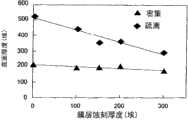
图4系一图表,其显示根据本发明实施例在不同膜层蚀刻厚度下,在基板特征密集区与疏离区中所获得的特征底部厚度;4 is a graph showing the bottom thickness of features obtained in feature-dense regions and isolated regions of the substrate under different film layer etching thicknesses according to an embodiment of the present invention;
图5系一图表,其显示根据本发明实施例在不同膜层蚀刻厚度下,所获得的底部图案加载效应(patter nloading effect);FIG. 5 is a graph showing the bottom pattern loading effect (patter nloading effect) obtained under different film layer etching thicknesses according to an embodiment of the present invention;
图6显示一沉积处理实施例的流程图;Figure 6 shows a flow diagram of an embodiment of a deposition process;
图7为一图表,其显示根据本发明实施例执行一沉积处理过程中的膜层厚度;FIG. 7 is a graph showing film thickness during a deposition process performed according to an embodiment of the present invention;
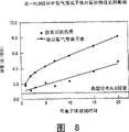
图8显示根据本发明实施例在一基板上沉积一膜层时,该膜层厚度对该基板暴露在前驱物中的时间做图的图表;8 shows a chart showing the thickness of the film layer as a graph of the time the substrate is exposed to the precursor when depositing a film layer on a substrate according to an embodiment of the present invention;
图9为根据本发明实施例在基板上的膜层沉积反应示意图;9 is a schematic diagram of a film deposition reaction on a substrate according to an embodiment of the present invention;
图10显示沉积处理另一实施例的流程图;Figure 10 shows a flow chart of another embodiment of a deposition process;
图11显示沉积处理又一实施例的流程图。Figure 11 shows a flow diagram of yet another embodiment of a deposition process.
具体实施方式Detailed ways
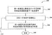
本发明提供一种在已形成的特征上沉积一共形介电层的方法与设备。可从此处理方法受益的膜层包含诸如氧化硅、氮氧化硅或氮化硅膜层等介电材料,这些膜层可做为间隙壁或蚀刻停止层等。这些膜层可能掺杂碳、掺杂氢或是含有其它化学物或元素,以修改其介电特性。该膜层也可掺杂碳或掺杂氮。举例而言,这些膜层可以是SiCN、SiOC、SiOCN、SiBN、SiBCN、SiC、BN或BCN膜层。在一方面中,由个别沉积且经过等离子体处理的数层薄膜所组成的组合膜层可提供比单一层厚介电层更加共形(conformal)的介电层。适合用于本文中所述处理方法的反应室包括


图1是沉积处理100的一实施例的流程图。沉积处理100的所有处理步骤可能在同一个反应室中执行。处理100始于步骤110,步骤110包括将一其表面上具有至少一个已形成特征的基板放置于一反应室中。该已形成的特征可以是任何种类的已形成特征,例如通孔、互连或栅极堆栈层。接着在薄介电层沉积步骤120中,利用CVD或PECVD处理来沉积一介电层。该薄介电层可能为例如氧化硅、氮氧化硅或氮化硅层。该膜层可掺杂碳或掺杂氮。该薄介电层的厚度可介于约1埃(
图1是一个总括性的流程图,以提供绘于第2、6与10-11图中的各别处理的处理大纲。第2、6与10-11图中与图1相似的处理步骤皆以相同的组件符号来表示。然而,也可以有些许的处理变化。Figure 1 is a general flow chart to provide a process outline for the individual processes depicted in Figures 2, 6 and 10-11. The processing steps in Figures 2, 6 and 10-11 that are similar to those in Figure 1 are denoted by the same reference numerals. However, slight processing variations are also possible.
图2为沉积处理200的实施例的流程图。如步骤202所示,将一其表面上具有至少一个已形成特征的基板放置于一反应室中。该特征具有一顶面、一侧面与一底面。如步骤204所示,一介电层沉积在该基板上。可利用CVD或PECVD来该介电层。该介电层可以是诸如氮化硅、氧化硅或氮氧化硅层等膜层。或者,该膜层可以是任何掺杂有碳或氮的上述膜层。通常,该介电层的沉积处理形成在该顶面的介电层厚度会比形成在底面与侧面上的介电层厚度要厚。随后,如步骤206所示,利用由含氧气体或含卤素气体所形成的等离子体来蚀刻该介电层。该含卤素气体选自于由氟、氯、溴及其组合物所构成的群组中。可使用氧气(O2)或其它含氧气气体来供应一氧等离子体。或可选择参考图1所述的厚度测定步骤来分析或估计该介电层的厚度,虽然此步骤并未显示于图2中。若蚀刻介电层的步骤206在该至少一个已形成特征上提供一所期望的介电层轮廓时,该处理方法终止于步骤208。所期望的轮廓可能一共形或实质共形的轮廓,其在该特征的侧面、顶面与底面上的厚度差异会比在沉积后且蚀刻前的介电层在这些面上的厚度差异要小。换句话说,也就是所期望的轮廓具有改善的阶梯覆盖性,即,该特征不同表面间的膜层厚度差的百分比较小。若蚀刻介电层的步骤206无法在该至少一个已形成特征上提供一所期望的介电层轮廓时,则执行一重复步骤210。该重复步骤210包括沉积一额外量的该介电层并且随后蚀刻该介电层的步骤。该重复步骤210可执行数次,举例而言可重复执行1次至100次,例如介于1次至6次之间,以在该至少一个已形成特征上获得所期望的介电层轮廓。FIG. 2 is a flow diagram of an embodiment of a
回到步骤206,可以在进行介电层沉积的同一个反应室中或是在不同反应室中蚀刻该介电层,而该不同的反应室与该沉积室可属于同一个集成工具中的一部分,且该不同的反应室可透过该集成工具的传送室而与该沉积室相连。含氧气体或含卤素气体可独立地引入该反应室中,或是合并一惰性气体一起引入该反应室中,而惰性气体可例如是氩气或氦气。可使用一原位生成或远程生成的等离子体来执行蚀刻步骤206。蚀刻步骤206的时间长度可至少为0.1秒,例如介于约0.1秒至约45秒之间,如介于约15秒至约45秒之间。可通过调整含卤素气体的流速与暴露时间来设计该蚀刻轮廓(etch profile)以配合该沉积轮廓(deposition profile)。例如,在该特征顶面上的蚀刻速率可能高于再该特征侧面或底面上的蚀刻速率。通常,顶面上的蚀刻速率比侧面或底面上的蚀刻速率要高约10%。在某些范例中,可能需要约50%的蚀刻速率。本文中定义50%的蚀刻速率系指一能移除掉50%的沉积介电层厚度的蚀刻处理。此外,沉积步骤204也可以是一个双阶段沉积处理(a two part deposition),例如以具有第一功率与第一前驱物分压的等离子体执行两秒,并且以具有第二功率与第二前驱物分压的等离子体执行额外两秒。Returning to step 206, the dielectric layer can be etched in the same chamber where the dielectric layer is deposited or in a different chamber, which can be part of the same integrated tool as the deposition chamber , and the different reaction chambers can be connected to the deposition chamber through the transfer chamber of the integrated tool. Oxygen-containing gas or halogen-containing gas can be introduced into the reaction chamber independently, or combined with an inert gas such as argon or helium.
在使用远程生成等离子体来执行蚀刻步骤206的实施例中,可通过在一远程等离子体源中使氧气或一含卤素气体暴露于微波能量下来产生等离子体,其中该含卤素气体选自于由氟、氯、溴及其组合物所构成的群组中,并且该远程等离子体源连接至用来沉积介电层的反应室。例如,可利用能提供反应性氟物质的三氟化氮(NF3)来产生这些离子体。可以介于约10sccm至约20slm之间的流速将三氟化氮导入反应室中。三氟化氮也可与诸如氩气或氦气等稀释气体一同导入反应室中。氩气与氦气亦有助于维持反应室中的等离子体。可以介于约100sccm至约20slm之间的流速将三氟化氮导入反应室中。蚀刻过程中的反应室压力可介于约10毫托至约760托之间,并且反应室中的基板支撑件温度可设定在介于约100℃至约650℃之间。In embodiments where remotely generated plasma is used to perform
在使用原位(即在反应室中)生成的等离子体来执行蚀刻步骤206的实施例中,可使用射频功率来产生这些离子体。射频功率可具有一高频率,例如介于约1百万赫(MHz)至约13.56百万赫之间,如介于约2百万赫至约13.56百万赫之间;可具有一介于约100千赫至约1百万赫之间的低频率,例如约介于100千赫至约400千赫之间;或者可具有一混合频率,其包含一介于1百万赫至13.56百万赫之间的频率(例如约2百万赫至约13.56百万赫)以及一介于约100千赫至约1百万赫之间的低频率(例如约100千赫至约400千赫)。作为蚀刻气体并选自于氟、氯、溴及其组合物所构成的群组中的含卤素气体可以是三氟化氮,或是一含碳及氟的气体,例如四氟化碳(CF4)或八氟化二碳(C4F8)。可以介于约10sccm至约20slm的流速将氧或含卤素气体导入该反应室中。该氧或含卤素气体可与作为稀释气体的氩气或氦气一同导入该反应室中。氩气与氦气亦有助于维持反应室中的等离子体。可以介于约100sccm至约20slm的流速将氩气或氦气导入该反应室中。蚀刻过程中的反应室压力可能介于约10毫托至约760托之间,并且反应室中基板支撑件的温度可设定在介于约100℃至约650℃之间。反应室中,一喷头电极与一基板支撑件电极之间的间距可介于约100密耳(mil)至约3000密耳之间。可调整该间距来控制等离子体的稳定性。In embodiments where
本发明的多个实施例包含这些具有单一沉积步骤204与单一蚀刻步骤206的处理方法,以及这些包含一重复步骤210的处理方法,其中该重复步骤210中包含多个沉积与蚀刻步骤。当一介电层,与该介电层在特征顶面上的蚀刻速率相比,其在特征侧面上具有高蚀刻速率时,执行一包含单一沉积步骤与单一蚀刻步骤的处理方法。例如,该侧面上的蚀刻速率可能至少约为该介电层从该顶面上蚀刻的速率的10%。可提供在特征侧面上的离子轰击低于在特征顶面上的离子轰击的介电沉积处理,能够造成该特征侧面上的介电蚀刻速率高于该特征底面或顶面上的介电蚀刻速率的结果。Embodiments of the invention include those processes having a
通过使多个不同厚度的沉积介电层的蚀刻材料厚度保持固定,并进而改变这些进行蚀刻的介电层的百分比例,发现到对于这些厚度高达1000埃的介电层而言,这些包含单一沉积步骤与单一蚀刻步骤的处理方法的底部图案加载效应系与介电层厚度无关联。By keeping the etch material thickness constant for a number of deposited dielectric layers of different thicknesses, and thereby varying the percentage of these dielectric layers that were etched, it was found that for these dielectric layers up to 1000 Angstroms thick, these contained a single The bottom pattern loading effect of the deposition step and single etch step process is independent of the dielectric layer thickness.
针对一介电层(与该介电层在特征顶面上的蚀刻速率相比,其在特征侧面上具有较低蚀刻速率),可执行一包含多个沉积与蚀刻步骤的处理方法。例如,该侧面上的蚀刻速率可能低于约该介电层从该顶面上蚀刻的速率的10%。可通过在蚀刻该介电层之前与之后,利用SEM或TEM断面来测定位在特征底面、侧面与顶面处的介电层厚度,并计算出单位蚀刻时间所移除的厚度,以测定出蚀刻速率。提高沉积与蚀刻的循环次数可改善图案加载效应。For a dielectric layer that has a lower etch rate on the sides of the feature compared to the etch rate of the dielectric layer on the top surface of the feature, a process may be performed that includes multiple deposition and etch steps. For example, the etch rate on the sides may be less than about 10% of the rate at which the dielectric layer is etched from the top surface. It can be determined by measuring the thickness of the dielectric layer at the bottom, side and top surfaces of the feature by using SEM or TEM sections before and after etching the dielectric layer, and calculating the thickness removed per unit etching time. etch rate. Increasing the number of cycles of deposition and etching can improve the pattern loading effect.
在一示范实施例中,可执行一包含两次或三次沉积与蚀刻循环的处理方法来形成欲做为蚀刻终止衬层且特征尺寸为90纳米或更小的介电层。每个循环可沉积厚度约介于300埃至约400埃之间的介电层,并且每个蚀刻循环可蚀刻介于约100埃至200埃之间的介电层厚度。In an exemplary embodiment, a process comprising two or three deposition and etch cycles may be performed to form a dielectric layer intended to be an etch stop liner with a feature size of 90 nm or less. Each cycle can deposit a dielectric layer with a thickness between about 300 angstroms and about 400 angstroms, and each etch cycle can etch the dielectric layer with a thickness between about 100 angstroms and about 200 angstroms.
本发明实施例的示范性测试结果显示出,可控制蚀刻轮廓,使其配合提供在特征顶面上的蚀刻速率高于在特征底面与侧面上的蚀刻速率的沉积轮廓。图3A是根据现有技术而形成在基板306的特征304上的一介电层302的SEM示意图。该介电层具有不均匀的轮廓,其在特征顶面308上的厚度大于在特征侧面310与底面312的厚度。图3B显示根据本发明实施例而形成在特征304上的一介电层320的SEM示意图。在特征304上,该介电层320的轮廓比该介电层302的轮廓更加均匀一致。Exemplary test results of embodiments of the present invention show that the etch profile can be controlled to cooperate to provide a deposition profile with a higher etch rate on the top surface of the feature than on the bottom and sides of the feature. 3A is an SEM schematic of a
已形成的特征断面的扫描式电子显微照片亦显示出,以含有流量50sccm的NF3、3公升(L)的氩气、频率350千赫的100瓦(W)低频射频功率、1.5托的反应室压力以及1000密耳的间隔距离的条件来执行NF3等离子体蚀刻持续45秒,能使氮化硅介电层的底部图案加载效应(PLE)降低约30%(PLE从67%降低至41%),并且此蚀刻处理可用来调整其它介电膜层沉积处理的阶梯覆盖性。该蚀刻处理不会影响膜应力。侧壁负载效应则从46%降至33%,以及顶面负载效应则从10%降至3%。当通过各部位(portion)上的膜层厚度之间的膜厚差异百分比,例如具有少量特征的基板区域(疏离区)中一特征的底面、顶面或侧面上的膜层厚度与具有高特征密度的基板区域(密集区)中一特征相应部位上的膜层厚度间的差异百分比,来测量图案加载效应时,较低图案加载效应百分比系反应出基板表面具有较高的膜厚均匀度。Scanning electron micrographs of the formed characteristic cross-sections also show that, with NF3 at a flow rate of 50 sccm, 3 liters (L) of argon, 100 watts (W) of low frequency RF power at a frequency of 350 kHz, 1.5 Torr Performing NF3 plasma etch for 45 seconds at chamber pressure and a standoff distance of 1000 mils can reduce the bottom pattern loading effect (PLE) of the silicon nitride dielectric layer by about 30% (PLE is reduced from 67% to 41%), and this etching process can be used to adjust the step coverage of other dielectric film deposition processes. This etching process does not affect film stress. The sidewall loading effect is reduced from 46% to 33%, and the top surface loading effect is reduced from 10% to 3%. When passing through the percentage of film thickness difference between the film thickness on each portion, for example, the film thickness on the bottom, top or side of a feature in a substrate area with few features (isolated area) and the film thickness on the bottom surface, top surface or side of a feature with high features When the pattern loading effect is measured by the percentage difference between the thickness of the film layer on a corresponding part of a feature in a dense substrate area (dense area), a lower percentage of the pattern loading effect reflects a higher film thickness uniformity on the substrate surface.
第4与5图显示出以50sccm的NF3、3升(L)氩气、100瓦且350千赫的低频射频功率、1.5托的反应室压力以及1000密耳的间距的条件对具有特征疏离(iso)区与特征密集区的基板进行NF3蚀刻时,蚀刻时间长度(可用膜层蚀刻厚度来表示)对于底面介电层厚度以及图案加载效应的个别影响。可使用约15至45秒的蚀刻时间(etch period),其相当于约100埃至300埃的膜层蚀刻厚度。使用较长的蚀刻时间明显改善了该底面图案加载效应,即约30%。Figures 4 and 5 show that the conditions of 50 sccm of NF3 , 3 liters (L) of argon, 100 W and 350 kHz of low-frequency RF power, 1.5 Torr of chamber pressure, and 1000 mils of separation have characteristic separation When performing NF3 etching on the substrate in the (iso) area and the feature-dense area, the etching time length (expressed by the etching thickness of the film layer) has an individual influence on the thickness of the bottom dielectric layer and the pattern loading effect. An etch period of about 15 to 45 seconds can be used, which corresponds to a film etch thickness of about 100 angstroms to 300 angstroms. Using a longer etch time significantly improves the bottom pattern loading effect, ie about 30%.
使用三氟化氮(NF3)做为施用在氮化硅介电层上的含氟蚀刻气体,来比较图案加载效应及底面厚度与该蚀刻种类之间的关系。以一包含沉积厚度400埃的氮化硅介电层、将该氮化硅介电层蚀刻掉200埃的厚度以及随后沉积450埃的氮化硅介电层的步骤的处理为例,来比较没有蚀刻、功率为100瓦的低频射频等离子体蚀刻、功率为50瓦的高频射频等离子体蚀刻以及远程等离子体源蚀刻对于该处理的影响。低频射频等离子体蚀刻以及高频射频等离子体蚀刻得到相同的图案加载效应结果,然而远程等离子体源蚀刻则造成更大的图案加载效应并且造成超过20%的蚀刻速率不均匀性。虽然在远程等离子体蚀刻方法中的蚀刻轮廓更具等向性,然而当使用原位射频方法中的鞘区电压(sheath voltage)方向性地加速蚀刻物质朝向基板表时,相较于远程等离子体蚀刻方法而言,相信原位射频等离子体蚀刻方法能更有效地提供与沉积轮廓相似的蚀刻轮廓,也就是说,原位射频等离子体蚀刻方法在特征顶面上的蚀刻速率较快且特征侧面上的蚀刻速率较慢。Nitrogen trifluoride (NF3 ) was used as the fluorine-containing etching gas applied on the silicon nitride dielectric layer to compare the pattern loading effect and the relationship between the bottom thickness and the etching type. As an example, a process comprising the steps of depositing a silicon nitride dielectric layer to a thickness of 400 angstroms, etching the silicon nitride dielectric layer to a thickness of 200 angstroms, and subsequently depositing a silicon nitride dielectric layer of 450 angstroms will be compared No etching, low frequency RF plasma etching at 100 watts, high frequency RF plasma etching at 50 watts, and remote plasma source etching on the process. Low frequency RF plasma etching as well as high frequency RF plasma etching resulted in the same pattern loading effect, whereas remote plasma source etching caused a larger pattern loading effect and caused etch rate non-uniformity of more than 20%. Although the etch profile in the remote plasma etch method is more isotropic, when using the sheath voltage in the in situ RF method to directionally accelerate the etch species towards the surface of the substrate, compared to the remote plasma etch In terms of etching methods, it is believed that the in situ RF plasma etch method is more effective in providing an etch profile similar to the deposition profile, that is, the in situ RF plasma etch method has a faster etch rate on the top surface of the feature and a higher etch rate on the side of the feature. The etch rate is slower.
虽然图2的实施例主要以氮化硅(SiN)层来叙述,然而图2的实施例也可用于他种介电层,例如氧化硅(SiO)、氮化硅(SiN)、碳氮化硅(SiCN)、碳氧化硅(SiOC)、碳氮氧化硅(SiOCN)、硼氮化硅(SiBN)、硼碳氮化硅(SiBCN)、碳化硅(SiC)、氮化硼(BN)或碳氮化硼(BCN)等膜层。对于含有碳的膜层,蚀刻步骤206包含一含氧气体与一含卤素气体,该含氧气体能提供用来蚀刻含碳层的反应性氧物质。含卤素气体及含氧气体可同时使用或者先后使用。例如,可将膜层先暴露于含氧气体所形成的等离子体中,随后在暴露至含卤素气体所形成的等离子体中。Although the embodiment of FIG. 2 is mainly described with a silicon nitride (SiN) layer, the embodiment of FIG. 2 can also be used for other dielectric layers, such as silicon oxide (SiO), silicon nitride (SiN), carbonitride Silicon (SiCN), silicon oxycarbide (SiOC), silicon oxycarbonitride (SiOCN), silicon boron nitride (SiBN), silicon boron carbon nitride (SiBCN), silicon carbide (SiC), boron nitride (BN) or Boron carbon nitride (BCN) and other films. For carbon-containing layers, etching
图6为沉积处理600的实施例的流程图。沉积处理600的所有处理步骤可在同一个反应室中执行。处理600始于步骤610,步骤610包括将一其表面上具有至少一个已形成特征的基板(即,一图案化的基板)放置于一反应室中。该已形成特征可以是任何一种已形成的特征,例如通孔、互连或栅极堆栈层。FIG. 6 is a flow diagram of an embodiment of a
在前驱物与等离子体步骤620的过程中,系于反应室中同时存在有等离子体与含硅前驱物的情况下,使该基板暴露至该含硅前驱物中,以执行介电层的沉积作用。该含硅前驱物可包括八甲基环四硅氧烷(octamethylcyclotetrasiloxane,OMCTS)、甲基二乙氧基硅烷(methyldiethoxysilane,MDEOS)、双(第三丁基胺基)硅烷(bis(tertiary-butylamino)silane,BTBAS)、三-二甲基胺基硅烷(tridimethylaminosilane,TriDMAS)、三-二甲基胺基硅烷(trisdimethylaminosilane,TrisDMAS)、硅烷(silane)、二硅烷(disilane)、二氯硅烷(dichlorosilane)、三氯硅烷(trichlorosilane)、二溴硅烷(dibromosilane)、四氯化硅(silicon tetrachloride)、四溴化硅(silicontetrabromide)或上述硅化物的组合物。在一方面中,OMCTS与硅烷为较佳的含硅前驱物。以介于约50瓦至3000瓦之间的功率以及13.56百万赫(MHz)及/或350千赫(kHz)的频率来提供这些离子体。这些选用性气体导入反应室的时间与含硅气体的时间相同,并且这些选用性气体包括氦、氮、氧、氧化亚氮(nitrous oxide,或称一氧化二氮,俗称笑气)与氩气。若需使用一额外气体时,导入反应室中的额外气体以氧气及/或氦气为佳。氦气与其它惰性气体可做为载气。During the precursor and
在步骤620将等离子体、前驱物以及选用性的数种额外气体通入反应室之后,接着在氧清洗步骤630中将诸如氧气或氧化亚氮等含氧气体导入反应室中。氧清洗步骤630的执行方式系将含氧气体通入反应室中持续一段时间并达到一选定的分压来清洗掉残留的含硅前驱物以及这些选用性的额外气体。接着,在氧等离子体处理步骤640中,将一含氧气体(例如氧气或氧化亚氮)通入反应室中。以约50瓦至约3000瓦的功率来提供这些离子体并且持续介于约0.1秒至约600秒之间的时间。After passing the plasma, precursors, and optionally several additional gases into the reaction chamber at
回到步骤620,可以介于约5sccm至约1000sccm的流速将含硅前驱物导入反应室中。可以介于约100sccm至约20000sccm的流速将一选用性载气,例如氦,导入反应室中。当将含硅前驱物通入反应室中以沉积膜层时,导入反应室中的含硅前驱物(如八甲基环四硅氧烷)流速比上载气(如氦)流速的比例约为1:1或是更高,例如介于约1:1至约1:100之间。反应室压力可大于约5毫托,例如介于约1.8托至约10托之间,以及反应室中的基板支撑件温度可介于约125℃至约580℃之间。较佳者,该温度低于约500℃。该含硅前驱物可通入反应室中持续一段足以沉积出厚度介于约5埃至约2000埃间的膜层的时间。例如,该含硅前驱物可通入反应室中并持续约0.1秒至约120秒之间的时间。Returning to step 620, the silicon-containing precursor may be introduced into the reaction chamber at a flow rate between about 5 sccm and about 1000 sccm. An optional carrier gas, such as helium, can be introduced into the reaction chamber at a flow rate between about 100 seem and about 20,000 seem. When the silicon-containing precursor is passed into the reaction chamber to deposit a film layer, the ratio of the flow rate of the silicon-containing precursor (such as octamethylcyclotetrasiloxane) introduced into the reaction chamber to the carrier gas (such as helium) flow rate is about 1:1 or higher, such as between about 1:1 and about 1:100. The reaction chamber pressure can be greater than about 5 mTorr, for example, between about 1.8 Torr and about 10 Torr, and the substrate support temperature in the reaction chamber can be between about 125°C and about 580°C. Preferably, the temperature is less than about 500°C. The silicon-containing precursor may be passed into the reaction chamber for a period of time sufficient to deposit a film having a thickness ranging from about 5 Angstroms to about 2000 Angstroms. For example, the silicon-containing precursor may be passed into the reaction chamber for a time between about 0.1 second and about 120 seconds.
可利用功率介于约50瓦至约3000瓦间以及频率约为13.56百万赫或350千赫的射频功率来提供在步骤620中的等离子体。该射频功率可施加于反应室的一喷头(即,气体分配组件)以及/或基板支撑件。该喷头与基板支撑件之间的间距大于约230密耳,例如约介于350密耳至约800密耳之间。The plasma in
随后,终止通入反应室中的含硅前驱物流以及射频功率,并且在步骤630中导入一含氧气体以清除掉任何残留在反应室中的含气前驱物,该含氧气体例如氧气、氧化亚氮或其组合物。该含氧气体可以介于100sccm至约20000sccm的流速通入反应室中。并且该含氧气体可持续通入反应室中一段时间,例如介于0.1秒至60秒之间。当含氧气体通入反应室中时,反应室压力可介于约5毫托至约10托之间,以及反应室中基板支撑件的温度可介于约125℃至约580℃之间。Subsequently, the flow of the silicon-containing precursor and the radio frequency power into the reaction chamber are terminated, and an oxygen-containing gas is introduced in
待清洗过反应室之后,如步骤640所述般,在反应室中执行氧等离子体处理,以处理该含硅前驱物沉积在基板上的膜层。可以介于100sccm至20000sccm之间的流速将含氧气体导入反应室中。含氧气体可持续通入反应室中一段时间,例如介于约0.1秒至约120秒之间。可在反应室中施加介于约50瓦至3000瓦以及约13.56百万赫及/或350千赫的射频功率来提供该氧气等离子体。当含氧气体流入反应室时,反应室压力可介于5毫托至约10托之间,且反应室中的基板支撑件温度可介于约125℃至约580℃之间。After the reaction chamber is cleaned, as described in
可通过中断RF功率以及通入反应室中的含氧气体流来停止氧等离子体处理。可选择性地,于厚度测定步骤650中分析或估计已沉积的介电层的厚度。若所沉积的膜层或多层薄膜的厚度等于或大于一所期望的指定厚度时,则处理600完成并止于该结束步骤660。在结束步骤660中,基板接受额外的处理并从反应室中移出。若厚度不等于或不大于所期望的指定厚度时,则在重复处理655中,重复执行沉积步骤620与等离子体处理步骤630。可令该厚度测定步骤650与该重复处理655反复执行数次,直到获得所期望的膜层厚度为止,例如可重复执行约1次至6次。Oxygen plasma treatment can be stopped by interrupting the RF power and flow of oxygen-containing gas into the reaction chamber. Optionally, the thickness of the deposited dielectric layer is analyzed or estimated in
若膜层厚度不等于或不大于所期望的指定厚度,则继续将含硅前驱物气流通入反应室中以沉积一额外量的介电层。随后,清洗该反应室并执行如上所述的氧等离子体处理。可执行多次的沉积、清洗以及等离子体处理循环,直到获得所期望的介电层厚度为止。If the film thickness is not equal to or greater than the desired specified thickness, continue to flow the silicon-containing precursor gas into the reaction chamber to deposit an additional amount of the dielectric layer. Subsequently, the reaction chamber is cleaned and oxygen plasma treatment as described above is performed. Multiple cycles of deposition, cleaning, and plasma treatment may be performed until the desired dielectric layer thickness is achieved.
使用OMCTS作为含硅前驱物与氦气来执行类似于图6实施例的实验性处理测试。将膜层沉积速率以及所形成的膜层中的甲基:氧基的比例对等离子体功率做图。当使用0至400瓦的等离子体功率进行实验,沉积速率在等离子体功率约300瓦的时候达到稳定期(plateau),以及该甲基:氧基的比例则在等离子体功率约400瓦的时候达到最低。An experimental processing test similar to the embodiment of FIG. 6 was performed using OMCTS as the silicon-containing precursor and helium. The film deposition rate and the ratio of methyl:oxyl groups in the formed film were plotted versus plasma power. When experiments were carried out using plasma powers from 0 to 400 watts, the deposition rate plateaued at about 300 watts of plasma power, and the methyl:oxyl ratios reached a plateau at about 400 watts of plasma power reach the minimum.
测试氦气与OMCTS的数种组合,以决定出其用来沉积介电层的最佳比例。当做为额外气体的氦气是做为含硅前驱物的OMCTS的两倍时,会得到具有最大厚度的膜层。此外,使用OMCTS所沉积的膜层、使用OMCTS与氧气等离子体在90毫托下所沉积的膜层、以及使用OMCTS和氧气等离子体在2托下所沉积的膜层的扫描式电子显微镜照片显示出,在三种膜层之中,以利用OMCTS和氧气等离子体在2托下所沉积的膜层能提供最佳的图案加载效应与阶梯覆盖效果。Several combinations of helium and OMCTS were tested to determine the optimum ratio for deposition of dielectric layers. When helium as the additional gas is twice as much as OMCTS as the silicon-containing precursor, the film with the maximum thickness is obtained. In addition, scanning electron micrographs of films deposited using OMCTS, films deposited using OMCTS and oxygen plasma at 90 mTorr, and films deposited using OMCTS and oxygen plasma at 2 Torr show It is shown that among the three kinds of film layers, the film layer deposited by using OMCTS and oxygen plasma under 2 Torr can provide the best pattern loading effect and step coverage effect.
比较氧化亚氮与氧气于氧等离子体处理步骤640中的使用效果。利用氧化亚氮等离子体所沉积的膜层以及利用氧化亚氮等离子体所沉积的膜层的扫描式电子显微镜照面显示出,该两种膜层之中,使用氧气等离子体所沉积出来的膜层具有较佳图案加载效应与阶梯覆盖效果。The effect of using nitrous oxide and oxygen in the oxygen
在一方面中,图6的实施例是一种脉冲膜层沉积处理(PLD),也就是数次的含硅前驱物脉冲之间穿插以氧等离子体处理,以提供连续数层的沉积薄膜,而这些薄膜形成一完整的膜层。图7显示在执行多次上述的沉积与等离子体循环的介电层沉积过程中,膜层厚度对沉积时间或循环次数做图的图形。图中标示出执行等离子体处理的时间点。图7显示出一不含等离子体处理的类似处理,该不含等离子体处理的处理中具有数个沉积速率明显下降的时间区段,同时本发明所提供的处理则没有会出现此种沉积速率明显下降的时间区段。图8显示,该不含等离子体处理的类似处理中每一个有等离子体存在下将含硅前驱物(OMCTS)通入反应室的时间区段内(图8中的等离子体浸润时间,plasma soak time)所沉积的膜层厚度,会小于根据本发明实施例的具有等离子体处理的处理中每一个有等离子体存在下将含硅前驱物通入反应室的时间区段内所沉积的膜层厚度。并注意到根据本发明处理所得到的该沉积速率比原子层沉积(ALD)处理的沉积速率要高出将近10倍。此外,本文中所叙述的处理方法可在传统化学气相沉积反应室中执行,例如PRODUCER PECVDTM反应室。In one aspect, the embodiment of FIG. 6 is a pulsed layer deposition process (PLD), that is, several pulses of silicon-containing precursors are interspersed with oxygen plasma treatment to provide successive layers of deposited films, And these thin films form a complete film layer. FIG. 7 shows a graph of film thickness versus deposition time or number of cycles during a dielectric layer deposition process in which the above-described deposition and plasma cycles are performed multiple times. The time points at which the plasma treatment was performed are indicated in the figure. Figure 7 shows a similar treatment without plasma treatment with several time periods in which the deposition rate drops significantly, while the treatment provided by the present invention does not exhibit such deposition rate time period of significant decline. Figure 8 shows that in this similar process without plasma treatment, each of the time intervals in which the silicon-containing precursor (OMCTS) is introduced into the reaction chamber in the presence of plasma (plasma soak time in Figure 8, plasma soak time) the thickness of the deposited film will be less than the film deposited in the time interval of each time period when the silicon-containing precursor is passed into the reaction chamber in the presence of plasma in the treatment with plasma treatment according to the embodiment of the present invention thickness. It is noted that the deposition rate obtained with the treatment according to the invention is nearly 10 times higher than that obtained with the atomic layer deposition (ALD) treatment. Additionally, the processing methods described herein can be performed in conventional chemical vapor deposition chambers, such as PRODUCER PECVD™ chambers.
曾经观察到沉积膜层中出现甲基(-CH3)的话可能会阻碍进一步(后续)的沉积作用,而氧等离子体处理被认为能够通过移除留在沉积膜层中的甲基来提高沉积速率。如果沉积膜层中的甲基基团并不是很多的话,那么氧等离子体处理能将甲基取代成羟基(-OH),羟基可在另一层含气前驱物的黏附过程中作为成核位置(nucleation sites)。图9显示在由八甲基环四硅氧烷(OMCTS)所沉积的膜层上执行一氧等离子体处理的作用效果。为了图标简单清楚,图中仅显示该膜层中的一个OMCTS分子。在图9的步骤902中,当有等离子体存在时,OMCTS会与含有Si-OH键的基板反应。等离子体会产生出OMCTS自由基。随后如步骤904所示,OMCTS自由基连接至基板的羟基。在步骤906中,含有氧气的氧等离子体处理将已沉积的OMCTS层中至少一个部份的甲基替换成羟基。It has been observed that the presence of methyl groups (-CH3) in the deposited film may hinder further (subsequent) deposition, and oxygen plasma treatment is thought to increase the deposition rate by removing the methyl groups remaining in the deposited film . If there are not many methyl groups in the deposited film, oxygen plasma treatment can replace the methyl groups with hydroxyl groups (-OH), which can serve as nucleation sites during the adhesion of another layer of gas-containing precursors (nucleation sites). Figure 9 shows the effect of an oxygen plasma treatment on a film deposited from octamethylcyclotetrasiloxane (OMCTS). For the simplicity and clarity of the diagram, only one OMCTS molecule in the film layer is shown in the figure. In
发现到当使用一自我饱和前驱物(self-saturating precursor)作为沉积膜层的前驱物,并使用如上所述的射频功率大小、间距、压力以及流速比例时,能够可靠地沉积出厚度约介于3埃至25埃之间的均匀介电薄层。利用本文中所提供的处理条件可得到在300毫米的单一基板内厚度变化幅度约1埃的膜层。如本文中所定义者,「自我饱和前驱物(self-saturatingprecursor)」系指一种能够在基板上沉积出一薄层的前驱物,例如可在基板上沉积出一分子层者。该薄介电层的存在会阻碍来自该前驱物的介电材料在沉积该薄层的处理条件下形成额外膜层的进一步沉积作用。OMCTS是较佳的自我饱和前驱物,因为OMCTS含有大量的甲基而使其能产生膜层的自我饱和沉积作用。换句话说,由于下方基板的表面能尽快地覆满OMCTS分子,而已沉积的膜层表面上的Si-CH3键会实质阻碍进一步的沉积作用,直到通过上述氧等离子体处理来移除部份的甲基为止,从而能够由OMCTS沉积出一第一共形膜层。因此,能够良好地控制着每层OMCTS分子层的沉积作用,从而提高最终膜层的阶梯覆盖效果。It was found that when using a self-saturating precursor as the precursor to deposit the film layer, and using the RF power level, spacing, pressure and flow rate ratio as described above, it is possible to reliably deposit thickness between about Uniform dielectric thin layers between 3 angstroms and 25 angstroms. Using the processing conditions provided herein, a film layer with a thickness variation range of about 1 Angstrom within a single substrate of 300 mm can be obtained. As defined herein, a "self-saturating precursor" refers to a precursor capable of depositing a thin layer on a substrate, such as one capable of depositing a molecular layer on a substrate. The presence of the thin dielectric layer hinders further deposition of dielectric material from the precursor to form additional layers under the processing conditions used to deposit the thin layer. OMCTS is a better self-saturation precursor, because OMCTS contains a large amount of methyl groups so that it can produce self-saturation deposition of the film layer. In other words, since the surface of the underlying substrate can be covered with OMCTS molecules as soon as possible, the Si-CH3 bonds on the surface of the deposited film will substantially hinder further deposition until part of the OMCTS is removed by the above-mentioned oxygen plasma treatment. methyl group, so that a first conformal film layer can be deposited by OMCTS. Therefore, the deposition of each OMCTS molecular layer can be well controlled, thereby improving the step coverage effect of the final film layer.
由扫描式电子显微镜的影像可证实,相较于利用传统等离子体增强化学气相沉积处理所沉积出的膜层而言,根据第6-9图的处理方法能提供改善的阶梯覆盖与较低的图案加载效应。As evidenced by scanning electron microscope images, the process according to Figures 6-9 provides improved step coverage and lower Pattern loading effect.
测量多个具有高特征密度(密集区)与低特征密度区域(疏离区)的图案化基板中位在特征侧面、底面与顶面上根据本发明实施例所沉积的氧化物层的沉积情形。在密集区中达到75%的侧面/顶面覆盖(sidewall/topcoverage),而疏离区中达到80%的侧面/顶面覆盖。在密集区中达到85%的底面/顶面覆盖(bottom/top coverage),以及在疏离区中达到95%的底面/顶面覆盖。特征顶面处所观察到的图案加载效应(PLE)为0%,以及在特征侧面与底面处所观察到的图案加载效应仅有10%。在一范例中,一氧化层沉积在深宽比为3.5的特征中的顶面厚度为420埃。该膜层在侧面上的厚度为275埃,以及其在底面上的厚度为345埃。因此,侧面/顶面的阶梯覆盖为66%,底面/顶面的阶梯覆盖为83%,以及侧面/底面的阶梯覆盖为80%。在另一范例中,一低介电常数的碳掺杂氧化层沉积在深宽比为3.5的特征中的顶面厚度为340埃。该层在侧面上的厚度为125埃,以及该层在底面上的厚度为210埃。因此,侧面/顶面的阶梯覆盖为35%,底面/顶面的阶梯覆盖为60%,以及侧面/底面的阶梯覆盖为58%。The deposition of oxide layers deposited according to embodiments of the present invention on the side, bottom and top surfaces of features in a plurality of patterned substrates having high feature density (dense regions) and low feature density regions (isolated regions) was measured. A sidewall/top coverage of 75% is achieved in dense areas and a sidewall/top coverage of 80% is achieved in depopulated areas. A bottom/top coverage of 85% is achieved in dense regions and a bottom/top coverage of 95% is achieved in depopulated regions. The pattern loading effect (PLE) observed at the top of the feature was 0%, and only 10% was observed at the side and bottom of the feature. In one example, an oxide layer was deposited with a thickness of 420 angstroms on top of features with an aspect ratio of 3.5. The thickness of the film layer was 275 angstroms on the sides and 345 angstroms on the bottom. Thus, the side/top step coverage is 66%, the bottom/top step coverage is 83%, and the side/bottom step coverage is 80%. In another example, a low-k carbon-doped oxide layer is deposited with a thickness of 340 angstroms on top of features with an aspect ratio of 3.5. The layer has a thickness of 125 angstroms on the sides and a thickness of 210 angstroms on the bottom. Thus, the side/top step coverage is 35%, the bottom/top step coverage is 60%, and the side/bottom step coverage is 58%.
虽然主要是以使用OMCTS做为含硅前驱物来沉积氧化硅膜层或掺杂碳的氧化硅膜层为范例来讨论上述实施例与结果,然而亦可使用其它的含硅前驱物。也可使用其它包含硅-氧(Si-O)或硅-氮(Si-N)骨架以及一个或多个与硅原子键合的烷基的含硅前驱物。此外,可使用其它的等离子体处理来形成他种膜层。例如,可如下第10与11图所述般,使用含硅前驱物来沉积一膜层并以一氮气等离子体来处理该膜层,已形成一共形的氮化硅层(SiN)。Although the above embodiments and results are mainly discussed using OMCTS as a silicon-containing precursor to deposit a silicon oxide film or a carbon-doped silicon oxide film as an example, other silicon-containing precursors may also be used. Other silicon-containing precursors comprising a silicon-oxygen (Si-O) or silicon-nitrogen (Si-N) backbone and one or more alkyl groups bonded to silicon atoms may also be used. Additionally, other plasma treatments may be used to form other layers. For example, a conformal silicon nitride (SiN) layer can be formed by depositing a layer using a silicon-containing precursor and treating the layer with a nitrogen plasma as described in FIGS. 10 and 11 below.
图10为沉积处理1000的实施例的流程图。起始步骤610、膜厚测定步骤650、重复步骤655以及结束步骤660系如上图6所述般。在沉积步骤1010中,将一含硅前驱物导入该反应室中。含硅前驱物可包含八甲基环四硅氧烷(octamethylcyclotetrasiloxane,OMCTS)、甲基二乙氧基硅烷(methyldiethoxysilane,MDEOS)、双(第三丁基胺基)硅烷(bis(tertiary-butylamino)silane,BTBAS)、三(二甲基胺基硅烷)(tridimethylaminosilane,TriDMAS),三-二甲基胺基硅烷(trisdimethylaminosilane,TrisDMAS)、硅烷(silane)、二硅烷(disilane)、二氯硅烷(dichlorosilane)、三氯硅烷(trichlorosilane)、二溴硅烷(dibromosilane)、四氯化硅(silicon tetrachloride)、四溴化硅(silicontetrabromide)或上述含硅化合物的组合物。硅烷为用于沉积处理1000中的较佳前驱物。沉积步骤1010可执行约2至5秒。接着在步骤1020中,将氮气导入反应室中以清洗反应室。随后,在步骤1030中,使用氨气用以在该反应室中提供等离子体。接续进行步骤1040,执行另一次氮气清洗步骤。从步骤1010至650的一次循环时间约为每循环60秒,并且沉机速率约为每循环2埃。处理1000提供共形覆盖,并且清洗效率(即,在氨气等离子体之前,清洗步骤移除含气前驱物的效率)能控制共形覆盖性。FIG. 10 is a flow diagram of an embodiment of a deposition process 1000 . The
图11为沉积处理1100的另一实施例的流程图。其起始步骤610、膜厚测定步骤650、重复步骤655以及结束步骤660系如上所述。在沉积步骤1110中,将一含硅前驱物导入该反应室中。在含硅前驱物步骤1110之后,可执行一选用性的氮气清洗步骤(未示出)。接着在等离子体步骤1120中,将一含氮前驱物的等离子体导入反应室中。含氮前驱物可包含氮、氨或氧化亚氮。氨是较佳的含氮前驱物。以沉积处理1100来说,从步骤1110至步骤650的一次循环时间约为30秒。沉积速率约为每循环3.5埃。FIG. 11 is a flow diagram of another embodiment of a
根据本发明实施例所提供的共形膜层可做为半导体器件中的不同膜层。举例而言,这些膜层可作为这些先沉积而后蚀柯以在晶体管栅极堆栈层周围形成间隙币的膜层,或者这些膜层可做为阻障层。The conformal film layer provided according to the embodiment of the present invention can be used as different film layers in a semiconductor device. For example, the layers can be used as the layers that are deposited and then etched to form spacers around the transistor gate stack, or the layers can be used as barrier layers.
上述处理的优点是这些处理可生产出具有较佳阶梯覆盖性与较低图案加载效应的膜层。并且可在同一个反应室中执行多个处理步骤循环,从而比这些需要多个反应室的处理需要更短的处理时间。并且总热预算与个别基板处理温度也比这些不使用等离子体的处理的热预算及温度要低。An advantage of the above treatments is that they produce films with better step coverage and lower pattern loading effects. And multiple cycles of processing steps can be performed in the same reaction chamber, thereby requiring shorter processing times than those that require multiple reaction chambers. Also, the overall thermal budget and individual substrate processing temperatures are lower than those for processes that do not use plasma.
虽然上述内容已说明本发明多个实施例,然而在不偏离本发明基本范围的情况下,仍可设计出其它与更尽一部的本发明实施例,并且本发明的范围当由权利要求所界定。Although the above description has described multiple embodiments of the present invention, other and more complete embodiments of the present invention can be designed without departing from the basic scope of the present invention, and the scope of the present invention should be defined by the claims defined.
Claims (20)
Translated fromChineseApplications Claiming Priority (9)
| Application Number | Priority Date | Filing Date | Title |
|---|---|---|---|
| US78827906P | 2006-03-31 | 2006-03-31 | |
| US60/788,279 | 2006-03-31 | ||
| US79025406P | 2006-04-07 | 2006-04-07 | |
| US60/790,254 | 2006-04-07 | ||
| US11/668,911US7601651B2 (en) | 2006-03-31 | 2007-01-30 | Method to improve the step coverage and pattern loading for dielectric films |
| US11/668,911 | 2007-01-30 | ||
| US11/693,005 | 2007-03-29 | ||
| US11/693,005US7780865B2 (en) | 2006-03-31 | 2007-03-29 | Method to improve the step coverage and pattern loading for dielectric films |
| PCT/US2007/065592WO2007118026A2 (en) | 2006-03-31 | 2007-03-30 | Step coverage and pattern loading for dielectric films |
Publications (2)
| Publication Number | Publication Date |
|---|---|
| CN101416293A CN101416293A (en) | 2009-04-22 |
| CN101416293Btrue CN101416293B (en) | 2011-04-20 |
Family
ID=38581763
Family Applications (1)
| Application Number | Title | Priority Date | Filing Date |
|---|---|---|---|
| CN2007800121574AExpired - Fee RelatedCN101416293B (en) | 2006-03-31 | 2007-03-30 | Method to improve the step coverage and pattern loading for dielectric films |
Country Status (4)
| Country | Link |
|---|---|
| KR (1) | KR20080106984A (en) |
| CN (1) | CN101416293B (en) |
| TW (2) | TW201415551A (en) |
| WO (1) | WO2007118026A2 (en) |
Cited By (2)
| Publication number | Priority date | Publication date | Assignee | Title |
|---|---|---|---|---|
| US11688851B2 (en) | 2015-01-09 | 2023-06-27 | Applied Materials, Inc. | Method of forming an anode structure with dielectric coating |
| US11827981B2 (en)* | 2020-10-14 | 2023-11-28 | Asm Ip Holding B.V. | Method of depositing material on stepped structure |
Families Citing this family (53)
| Publication number | Priority date | Publication date | Assignee | Title |
|---|---|---|---|---|
| US7935643B2 (en)* | 2009-08-06 | 2011-05-03 | Applied Materials, Inc. | Stress management for tensile films |
| US8574447B2 (en)* | 2010-03-31 | 2013-11-05 | Lam Research Corporation | Inorganic rapid alternating process for silicon etch |
| US9076646B2 (en) | 2010-04-15 | 2015-07-07 | Lam Research Corporation | Plasma enhanced atomic layer deposition with pulsed plasma exposure |
| US8637411B2 (en) | 2010-04-15 | 2014-01-28 | Novellus Systems, Inc. | Plasma activated conformal dielectric film deposition |
| US20110256734A1 (en) | 2010-04-15 | 2011-10-20 | Hausmann Dennis M | Silicon nitride films and methods |
| US9611544B2 (en)* | 2010-04-15 | 2017-04-04 | Novellus Systems, Inc. | Plasma activated conformal dielectric film deposition |
| US9257274B2 (en) | 2010-04-15 | 2016-02-09 | Lam Research Corporation | Gapfill of variable aspect ratio features with a composite PEALD and PECVD method |
| US9892917B2 (en) | 2010-04-15 | 2018-02-13 | Lam Research Corporation | Plasma assisted atomic layer deposition of multi-layer films for patterning applications |
| US9390909B2 (en) | 2013-11-07 | 2016-07-12 | Novellus Systems, Inc. | Soft landing nanolaminates for advanced patterning |
| US9373500B2 (en) | 2014-02-21 | 2016-06-21 | Lam Research Corporation | Plasma assisted atomic layer deposition titanium oxide for conformal encapsulation and gapfill applications |
| US9997357B2 (en) | 2010-04-15 | 2018-06-12 | Lam Research Corporation | Capped ALD films for doping fin-shaped channel regions of 3-D IC transistors |
| US8956983B2 (en) | 2010-04-15 | 2015-02-17 | Novellus Systems, Inc. | Conformal doping via plasma activated atomic layer deposition and conformal film deposition |
| US9685320B2 (en) | 2010-09-23 | 2017-06-20 | Lam Research Corporation | Methods for depositing silicon oxide |
| US20130045605A1 (en)* | 2011-08-18 | 2013-02-21 | Applied Materials, Inc. | Dry-etch for silicon-and-nitrogen-containing films |
| KR101975071B1 (en)* | 2011-09-23 | 2019-05-03 | 노벨러스 시스템즈, 인코포레이티드 | Plasma activated conformal dielectric film deposition |
| US8592328B2 (en) | 2012-01-20 | 2013-11-26 | Novellus Systems, Inc. | Method for depositing a chlorine-free conformal sin film |
| CN102832119B (en)* | 2012-07-03 | 2015-12-16 | 上海华力微电子有限公司 | The formation method of low temperature silicon dioxide film |
| CN102820220A (en)* | 2012-07-03 | 2012-12-12 | 上海华力微电子有限公司 | Forming method of low-temperature silica film |
| CN102768955A (en)* | 2012-07-03 | 2012-11-07 | 上海华力微电子有限公司 | Method for forming low-loading-effect thin film |
| KR102207992B1 (en) | 2012-10-23 | 2021-01-26 | 램 리써치 코포레이션 | Sub-saturated atomic layer deposition and conformal film deposition |
| SG2013083241A (en) | 2012-11-08 | 2014-06-27 | Novellus Systems Inc | Conformal film deposition for gapfill |
| JP6538300B2 (en) | 2012-11-08 | 2019-07-03 | ノベラス・システムズ・インコーポレーテッドNovellus Systems Incorporated | Method for depositing a film on a sensitive substrate |
| US20140131308A1 (en)* | 2012-11-14 | 2014-05-15 | Roman Gouk | Pattern fortification for hdd bit patterned media pattern transfer |
| CN103390703B (en)* | 2013-08-05 | 2016-08-17 | 聚灿光电科技股份有限公司 | The preparation method of low-damage and high-density film and there is the LED chip of this film |
| CN104752315B (en)* | 2013-12-25 | 2018-03-06 | 旺宏电子股份有限公司 | Semiconductor element and its manufacturing method |
| US9214334B2 (en) | 2014-02-18 | 2015-12-15 | Lam Research Corporation | High growth rate process for conformal aluminum nitride |
| CN105322013B (en)* | 2014-07-17 | 2020-04-07 | 联华电子股份有限公司 | Semiconductor device and method for forming the same |
| US9478438B2 (en) | 2014-08-20 | 2016-10-25 | Lam Research Corporation | Method and apparatus to deposit pure titanium thin film at low temperature using titanium tetraiodide precursor |
| US9478411B2 (en) | 2014-08-20 | 2016-10-25 | Lam Research Corporation | Method to tune TiOx stoichiometry using atomic layer deposited Ti film to minimize contact resistance for TiOx/Ti based MIS contact scheme for CMOS |
| KR20160061129A (en)* | 2014-11-21 | 2016-05-31 | 주식회사 원익아이피에스 | Method of fabricating stacked film |
| US9564312B2 (en) | 2014-11-24 | 2017-02-07 | Lam Research Corporation | Selective inhibition in atomic layer deposition of silicon-containing films |
| KR102362534B1 (en) | 2014-12-08 | 2022-02-15 | 주성엔지니어링(주) | Substrate disposition method |
| US10566187B2 (en) | 2015-03-20 | 2020-02-18 | Lam Research Corporation | Ultrathin atomic layer deposition film accuracy thickness control |
| US9502238B2 (en) | 2015-04-03 | 2016-11-22 | Lam Research Corporation | Deposition of conformal films by atomic layer deposition and atomic layer etch |
| WO2016196264A1 (en)* | 2015-06-05 | 2016-12-08 | Applied Materials, Inc. | Battery separator with dielectric coating |
| US10526701B2 (en) | 2015-07-09 | 2020-01-07 | Lam Research Corporation | Multi-cycle ALD process for film uniformity and thickness profile modulation |
| US20170178899A1 (en)* | 2015-12-18 | 2017-06-22 | Lam Research Corporation | Directional deposition on patterned structures |
| CN107437503A (en)* | 2016-05-26 | 2017-12-05 | 灿美工程股份有限公司 | Substrate processing method using same |
| US9773643B1 (en) | 2016-06-30 | 2017-09-26 | Lam Research Corporation | Apparatus and method for deposition and etch in gap fill |
| US10062563B2 (en) | 2016-07-01 | 2018-08-28 | Lam Research Corporation | Selective atomic layer deposition with post-dose treatment |
| US10037884B2 (en) | 2016-08-31 | 2018-07-31 | Lam Research Corporation | Selective atomic layer deposition for gapfill using sacrificial underlayer |
| JP6817168B2 (en) | 2017-08-25 | 2021-01-20 | 東京エレクトロン株式会社 | How to process the object to be processed |
| JP6913569B2 (en)* | 2017-08-25 | 2021-08-04 | 東京エレクトロン株式会社 | How to process the object to be processed |
| US10269559B2 (en) | 2017-09-13 | 2019-04-23 | Lam Research Corporation | Dielectric gapfill of high aspect ratio features utilizing a sacrificial etch cap layer |
| US10910216B2 (en) | 2017-11-28 | 2021-02-02 | Taiwan Semiconductor Manufacturing Co., Ltd. | Low-k dielectric and processes for forming same |
| KR102691504B1 (en)* | 2018-06-19 | 2024-08-01 | 어플라이드 머티어리얼스, 인코포레이티드 | Improved pulsed plasma deposition etch step coverage |
| CN110896050A (en)* | 2018-09-12 | 2020-03-20 | 长鑫存储技术有限公司 | Method for forming dielectric film |
| KR102513404B1 (en)* | 2018-09-21 | 2023-03-27 | 주식회사 원익아이피에스 | Method of forming SiCN layer |
| KR20210123404A (en) | 2019-02-27 | 2021-10-13 | 램 리써치 코포레이션 | Semiconductor Mask Reshaping Using a Sacrificial Layer |
| KR102726216B1 (en) | 2019-05-01 | 2024-11-04 | 램 리써치 코포레이션 | Modulated atomic layer deposition |
| JP2022534793A (en) | 2019-06-07 | 2022-08-03 | ラム リサーチ コーポレーション | In situ control of film properties during atomic layer deposition |
| JP7702419B2 (en) | 2020-02-28 | 2025-07-03 | ラム リサーチ コーポレーション | Multilayer hardmasks for defect reduction in EUV patterning - Patents.com |
| TW202510042A (en)* | 2023-05-25 | 2025-03-01 | 美商蘭姆研究公司 | Cyclic etching and deposition to control film profile |
Family Cites Families (17)
| Publication number | Priority date | Publication date | Assignee | Title |
|---|---|---|---|---|
| US5641710A (en)* | 1996-06-10 | 1997-06-24 | Taiwan Semiconductor Manufacturing Company, Ltd. | Post tungsten etch back anneal, to improve aluminum step coverage |
| US6303523B2 (en)* | 1998-02-11 | 2001-10-16 | Applied Materials, Inc. | Plasma processes for depositing low dielectric constant films |
| US6068884A (en)* | 1998-04-28 | 2000-05-30 | Silcon Valley Group Thermal Systems, Llc | Method of making low κ dielectric inorganic/organic hybrid films |
| US6297163B1 (en)* | 1998-09-30 | 2001-10-02 | Lam Research Corporation | Method of plasma etching dielectric materials |
| TW460408B (en)* | 1999-04-20 | 2001-10-21 | Applied Materials Inc | Remote plasma nitridation of silicon |
| JP4554011B2 (en)* | 1999-08-10 | 2010-09-29 | ルネサスエレクトロニクス株式会社 | Manufacturing method of semiconductor integrated circuit device |
| US6399208B1 (en)* | 1999-10-07 | 2002-06-04 | Advanced Technology Materials Inc. | Source reagent composition and method for chemical vapor deposition formation or ZR/HF silicate gate dielectric thin films |
| US6410462B1 (en)* | 2000-05-12 | 2002-06-25 | Sharp Laboratories Of America, Inc. | Method of making low-K carbon doped silicon oxide |
| TW447077B (en)* | 2000-07-17 | 2001-07-21 | Taiwan Semiconductor Mfg | Method for improving the characteristics of dielectric layer with a low dielectric constant formed by chemical vapor deposition |
| TW563202B (en)* | 2000-10-25 | 2003-11-21 | Ibm | An ultralow dielectric constant material as an intralevel or interlevel dielectric in a semiconductor device and an electronic device containing the same |
| US6531412B2 (en)* | 2001-08-10 | 2003-03-11 | International Business Machines Corporation | Method for low temperature chemical vapor deposition of low-k films using selected cyclosiloxane and ozone gases for semiconductor applications |
| TW497140B (en)* | 2001-10-09 | 2002-08-01 | Taiwan Semiconductor Mfg | Process system for plasma etching and chemical vapor deposition |
| JP2005510082A (en)* | 2001-11-16 | 2005-04-14 | トリコン ホールディングス リミティド | Formation of low-K dielectric layer |
| US6800566B2 (en)* | 2002-02-21 | 2004-10-05 | Taiwan Semiconductor Manufacturing Company | Adjustment of N and K values in a DARC film |
| US7335609B2 (en)* | 2004-08-27 | 2008-02-26 | Applied Materials, Inc. | Gap-fill depositions introducing hydroxyl-containing precursors in the formation of silicon containing dielectric materials |
| US6858542B2 (en)* | 2003-01-17 | 2005-02-22 | Freescale Semiconductor, Inc. | Semiconductor fabrication method for making small features |
| US7037855B2 (en)* | 2004-08-31 | 2006-05-02 | Asm Japan K.K. | Method of forming fluorine-doped low-dielectric-constant insulating film |
- 2007
- 2007-03-30CNCN2007800121574Apatent/CN101416293B/ennot_activeExpired - Fee Related
- 2007-03-30WOPCT/US2007/065592patent/WO2007118026A2/enactiveApplication Filing
- 2007-03-30TWTW102146174Apatent/TW201415551A/enunknown
- 2007-03-30TWTW096111415Apatent/TWI424498B/enactive
- 2007-03-30KRKR1020087026336Apatent/KR20080106984A/ennot_activeCeased
Cited By (3)
| Publication number | Priority date | Publication date | Assignee | Title |
|---|---|---|---|---|
| US11688851B2 (en) | 2015-01-09 | 2023-06-27 | Applied Materials, Inc. | Method of forming an anode structure with dielectric coating |
| US12057574B2 (en) | 2015-01-09 | 2024-08-06 | Applied Materials, Inc. | Method of forming an anode structure with dielectric coating |
| US11827981B2 (en)* | 2020-10-14 | 2023-11-28 | Asm Ip Holding B.V. | Method of depositing material on stepped structure |
Also Published As
| Publication number | Publication date |
|---|---|
| KR20080106984A (en) | 2008-12-09 |
| WO2007118026A3 (en) | 2008-01-10 |
| TW200816310A (en) | 2008-04-01 |
| TWI424498B (en) | 2014-01-21 |
| CN101416293A (en) | 2009-04-22 |
| TW201415551A (en) | 2014-04-16 |
| WO2007118026A2 (en) | 2007-10-18 |
Similar Documents
| Publication | Publication Date | Title |
|---|---|---|
| CN101416293B (en) | Method to improve the step coverage and pattern loading for dielectric films | |
| TWI842531B (en) | Method of topology-selective film formation of silicon oxide | |
| US7780865B2 (en) | Method to improve the step coverage and pattern loading for dielectric films | |
| TWI873306B (en) | Method for fabricating layer structure having target topological profile | |
| US7601651B2 (en) | Method to improve the step coverage and pattern loading for dielectric films | |
| CN110313051B (en) | Densification of silicon carbide films using remote plasma treatment | |
| JP4439860B2 (en) | Method for forming film on semiconductor substrate | |
| TWI673826B (en) | Flowable film curing penetration depth improvement and stress tuning | |
| US9023737B2 (en) | Method for forming conformal, homogeneous dielectric film by cyclic deposition and heat treatment | |
| CN102097364B (en) | Hard mask material | |
| US8445075B2 (en) | Method to minimize wet etch undercuts and provide pore sealing of extreme low k (k<2.5) dielectrics | |
| KR102012532B1 (en) | Plasma activated conformal dielectric film deposition | |
| US20170365462A1 (en) | Remote plasma based deposition of oxygen doped silicon carbide films | |
| CN101378850A (en) | Enhanced Remote Plasma Source Cleaning for Dielectric Coatings | |
| CN113195786A (en) | Remote hydrogen plasma exposure and doped or undoped silicon carbide deposition for gap fill | |
| JP2014509081A (en) | Densification after flattening | |
| KR20050034566A (en) | Method of manufacturing silicon carbide film | |
| KR20080092448A (en) | How to Enhance Remote Plasma Source Cleaning for Dielectric Films | |
| CN116487246A (en) | Remote plasma-based deposition of oxygen-doped silicon carbide films | |
| CN102460679A (en) | Boron film interface engineering | |
| CN101061256A (en) | High-power dielectric seasoning for stable wafer-to-wafer thickness uniformity of dielectric CVD films | |
| TWI392024B (en) | Method to minimize wet etch undercuts and provide pore sealing of extreme low k (k<2.5) dielectrics | |
| US20050133059A1 (en) | Method for cleaning a plasma enhanced CVD chamber | |
| US12234549B2 (en) | Method of in situ ceramic coating deposition | |
| TWI766014B (en) | Method for forming silicon nitride film selectively on sidewalls or flat surfaces of trenches |
Legal Events
| Date | Code | Title | Description |
|---|---|---|---|
| C06 | Publication | ||
| PB01 | Publication | ||
| C10 | Entry into substantive examination | ||
| SE01 | Entry into force of request for substantive examination | ||
| C14 | Grant of patent or utility model | ||
| GR01 | Patent grant | ||
| C56 | Change in the name or address of the patentee | ||
| CP01 | Change in the name or title of a patent holder | Address after:American California Patentee after:Applied Materials Inc. Address before:American California Patentee before:Applied Materials Inc. | |
| CF01 | Termination of patent right due to non-payment of annual fee | Granted publication date:20110420 Termination date:20150330 | |
| EXPY | Termination of patent right or utility model |