CN101414070B - Touch electrode layer and display panel - Google Patents
Touch electrode layer and display panelDownload PDFInfo
- Publication number
- CN101414070B CN101414070BCN2008101796997ACN200810179699ACN101414070BCN 101414070 BCN101414070 BCN 101414070BCN 2008101796997 ACN2008101796997 ACN 2008101796997ACN 200810179699 ACN200810179699 ACN 200810179699ACN 101414070 BCN101414070 BCN 101414070B
- Authority
- CN
- China
- Prior art keywords
- touch
- electrode pattern
- control electrode
- lower floor
- upper strata
- Prior art date
- Legal status (The legal status is an assumption and is not a legal conclusion. Google has not performed a legal analysis and makes no representation as to the accuracy of the status listed.)
- Active
Links
- 239000000758substrateSubstances0.000claimsabstractdescription37
- 239000010410layerSubstances0.000claimsdescription176
- 239000000463materialSubstances0.000claimsdescription11
- 239000011241protective layerSubstances0.000claimsdescription9
- 229910052751metalInorganic materials0.000claimsdescription5
- 239000002184metalSubstances0.000claimsdescription5
- 239000004020conductorSubstances0.000claimsdescription4
- 238000009413insulationMethods0.000claimsdescription4
- 230000001681protective effectEffects0.000claims2
- 239000010408filmSubstances0.000description17
- 239000004973liquid crystal related substanceSubstances0.000description15
- 230000003071parasitic effectEffects0.000description10
- 230000002093peripheral effectEffects0.000description9
- 238000005401electroluminescenceMethods0.000description7
- 239000011521glassSubstances0.000description3
- 239000010409thin filmSubstances0.000description3
- 239000000470constituentSubstances0.000description2
- 230000000694effectsEffects0.000description2
- AMGQUBHHOARCQH-UHFFFAOYSA-Nindium;oxotinChemical compound[In].[Sn]=OAMGQUBHHOARCQH-UHFFFAOYSA-N0.000description2
- 150000002739metalsChemical class0.000description2
- 238000000034methodMethods0.000description2
- 229920000642polymerPolymers0.000description2
- 230000035945sensitivityEffects0.000description2
- XUIMIQQOPSSXEZ-UHFFFAOYSA-NSiliconChemical compound[Si]XUIMIQQOPSSXEZ-UHFFFAOYSA-N0.000description1
- 229910021417amorphous siliconInorganic materials0.000description1
- 230000008878couplingEffects0.000description1
- 238000010168coupling processMethods0.000description1
- 238000005859coupling reactionMethods0.000description1
- 238000010586diagramMethods0.000description1
- 230000005684electric fieldEffects0.000description1
- 238000005516engineering processMethods0.000description1
- 229910010272inorganic materialInorganic materials0.000description1
- 239000011147inorganic materialSubstances0.000description1
- 238000004519manufacturing processMethods0.000description1
- 238000012986modificationMethods0.000description1
- 230000004048modificationEffects0.000description1
- 239000011368organic materialSubstances0.000description1
- 239000004033plasticSubstances0.000description1
- 229910021420polycrystalline siliconInorganic materials0.000description1
- 229920005591polysiliconPolymers0.000description1
- 229910052710siliconInorganic materials0.000description1
- 239000010703siliconSubstances0.000description1
- 150000003384small moleculesChemical class0.000description1
Images


Landscapes
- Position Input By Displaying (AREA)
Abstract
Description
Translated fromChinese【技术领域】【Technical field】
本发明是有关于一种触控电极层以及显示面板,且特别是有关于一种可降低触控电极层与显示面板内的电极层之间的寄生电容的触控电极层以及具有此触控电极层的显示面板。 The present invention relates to a touch electrode layer and a display panel, and in particular to a touch electrode layer capable of reducing the parasitic capacitance between the touch electrode layer and the electrode layer in the display panel, and a touch electrode layer with the touch control electrode layer. The electrode layer of the display panel. the
【背景技术】【Background technique】
一般现有的触控显示面板,其若以触控功能的设计原理分类大致分为电容式、电阻式以及感光式等。若以触控功能的结构分类则可分为外贴式及内嵌式两种。电容式触控显示面板因具有较高的开口率及较好的讯噪比,故成为目前市面上主流新开发的趋势。而内嵌式触控显示面板的厚度又比外贴式触控显示面板更为轻薄,所以,基于上述原因,内嵌式的电容触控显示面板的原理设计可望达到更好的规格及表现。 Generally, existing touch display panels can be roughly classified into capacitive, resistive, and photosensitive types based on the design principle of the touch function. According to the structural classification of the touch function, it can be divided into two types: external sticker type and built-in type. Capacitive touch display panels have become a mainstream new development trend in the market due to their higher aperture ratio and better signal-to-noise ratio. The thickness of the in-cell touch display panel is thinner than that of the external touch display panel. Therefore, based on the above reasons, the principle design of the in-cell capacitive touch display panel is expected to achieve better specifications and performance. . the
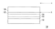
图1绘示为现有的液晶显示面板的剖面示意图。请参照图1,现有的液晶显示面板100包括第一基板102、画素数组(pixel array)103、液晶层(LiquidCrystal,LC)104、氧化铟锡(ITO)电极膜105以及第二基板108。画素数组103配置于第一基板102上,电极膜105位于第二基板108上,而液晶显示介质104则介于第一基板102和第二基板108之间。 FIG. 1 is a schematic cross-sectional view of a conventional liquid crystal display panel. Referring to FIG. 1 , a conventional liquid
就现有的内嵌式电容触控显示面板而言,电容式触控电极内嵌于液晶显示面板100的位置主要有两个:其分别为图1中的位置a或位置b。 As far as the existing in-cell capacitive touch display panel is concerned, there are mainly two positions where the capacitive touch electrodes are embedded in the liquid crystal display panel 100 : they are position a or position b in FIG. 1 . the
然而,随着消费性电子产品的轻薄短小发展趋势,液晶显示面板在使用上有了玻璃薄化的需求。所以当电容式触控电极内嵌于图1的位置a时,液晶显示面板会因为玻璃的薄化,而增加触控电极与电极膜105间的寄生电容。如此一来,将使得触控功能的扫瞄信号与液晶显示面板本身的驱动信号互相干扰 (coupling),进而导致显示功能和触控功能的信号错误。另外,当电容式触控电极内嵌于位置b时,液晶显示面板会因为触控电极跟电极膜105之间距离的更加靠近,而产生更大的寄生电容,因而导致信号干扰情况更为严重。 However, with the development trend of thinner, lighter and smaller consumer electronic products, there is a demand for glass thinning in the use of liquid crystal display panels. Therefore, when the capacitive touch electrodes are embedded in the position a in FIG. 1 , the liquid crystal display panel will increase the parasitic capacitance between the touch electrodes and the
【发明内容】【Content of invention】
因此,本发明提供一种触控电极层,其可降低触控电极与显示面板内的电极膜之间的寄生电容。 Therefore, the present invention provides a touch electrode layer, which can reduce the parasitic capacitance between the touch electrode and the electrode film in the display panel. the
本发明提供一种显示面板,其具有上述触控电极层。 The present invention provides a display panel, which has the above-mentioned touch electrode layer. the
本发明提出一种显示面板,其包括一第一基板、一第二基板以及一显示介质。显示介质位于第一基板和第二基板之间。第一基板上包括设置有一画素数组。第二基板上包括设置有一触控电极层。此触控电极层包括多条第一触控电极以及多条第二触控电极。第一触控电极沿第一方向排列,每一条第一触控电极由多个第一上层触控电极图案以及多个第一下层遮蔽电极图案交错排列而成,且每一第一上层触控电极图案与邻接的第一下层遮蔽电极图案电性连接。第二触控电极沿第二方向排列,每一条第二触控电极由多个第二上层触控电极图案以及多个第二下层遮蔽电极图案交错排列而成,且每一第二上层触控电极图案与邻接的第二下层遮蔽电极图案电性连接。 The invention provides a display panel, which includes a first substrate, a second substrate and a display medium. The display medium is located between the first substrate and the second substrate. A pixel array is arranged on the first substrate. A touch electrode layer is disposed on the second substrate. The touch electrode layer includes a plurality of first touch electrodes and a plurality of second touch electrodes. The first touch electrodes are arranged along the first direction, and each first touch electrode is formed by a plurality of first upper-layer touch electrode patterns and a plurality of first lower-layer shielding electrode patterns, and each first upper-layer touch electrode The control electrode pattern is electrically connected to the adjacent first lower layer shielding electrode pattern. The second touch electrodes are arranged along the second direction, and each second touch electrode is formed by a plurality of second upper-layer touch electrode patterns and a plurality of second lower-layer shielding electrode patterns, and each second upper-layer touch electrode The electrode pattern is electrically connected to the adjacent second lower layer shielding electrode pattern. the
在本发明的一实施例中,上述的显示面板更包括一保护层以及一电极膜,保护层覆盖于触控电极层上,且电极膜位于保护层上。 In an embodiment of the present invention, the above-mentioned display panel further includes a protective layer and an electrode film, the protective layer covers the touch electrode layer, and the electrode film is located on the protective layer. the
在本发明的一实施例中,上述位于触控电极层与电极膜之间的保护层厚度为10~50微米。 In an embodiment of the present invention, the protective layer between the touch electrode layer and the electrode film has a thickness of 10-50 microns. the
在本发明的一实施例中,上述每一第一上层触控电极图案设置于对应的第二下层遮蔽电极图案上方。 In an embodiment of the present invention, each of the above-mentioned first upper layer touch electrode patterns is disposed above the corresponding second lower layer shielding electrode patterns. the
在本发明的一实施例中,上述第一上层触控电极图案与第二上层触控电极图案共平面,而第一下层遮蔽电极图案与第二下层遮蔽电极图案共平面。 In an embodiment of the present invention, the first upper layer touch electrode pattern and the second upper layer touch electrode pattern are coplanar, and the first lower layer shielding electrode pattern is coplanar with the second lower layer shielding electrode pattern. the
在本发明的一实施例中,上述第一上层触控电极图案的尺寸与第二下层遮蔽电极图案的尺寸实质相同,且第二上层触控电极图案与第一下层遮蔽电极图案尺寸实质上相同。In an embodiment of the present invention, the size of the first upper layer touch electrode pattern is substantially the same as the size of the second lower layer shielding electrode pattern, and the size of the second upper layer touch electrode pattern is substantially the same as that of the first lower layer shielding electrode pattern. same.
在本发明的一实施例中,上述每一第一上层触控电极图案、每一第一下层遮蔽电极图案、每一第二上层触控电极图案或每一第二下层遮蔽电极图案的面积为一单位触控面积的1/2~2/3。 In an embodiment of the present invention, the area of each of the above-mentioned first upper layer touch electrode patterns, each first lower layer shielding electrode pattern, each second upper layer touch electrode pattern or each second lower layer shielding electrode pattern It is 1/2 to 2/3 of a unit touch area. the
在本发明的一实施例中,上述的显示面板更包括多个第一接触结构以及多个第二接触结构。每一第一接触结构位于相邻的第一上层触控电极图案与第一下层遮蔽电极图案之间,以电性连接第一上层触控电极图案与第一下层电极遮蔽电极图案。每一第二接触结构位于相邻的第二上层触控电极图案与第二下层遮蔽电极图案之间,以电性连接第二上层触控电极图案与第二下层电极遮蔽电极图案。 In an embodiment of the present invention, the above-mentioned display panel further includes a plurality of first contact structures and a plurality of second contact structures. Each first contact structure is located between the adjacent first upper layer touch electrode pattern and the first lower layer shielding electrode pattern to electrically connect the first upper layer touch electrode pattern and the first lower layer electrode shielding electrode pattern. Each second contact structure is located between the adjacent second upper layer touch electrode pattern and the second lower layer shielding electrode pattern to electrically connect the second upper layer touch electrode pattern and the second lower layer electrode shielding electrode pattern. the
在本发明的一实施例中,上述每一第一接触结构以及每一第二接触结构为至少一接触插塞或是一连续接触结构。 In an embodiment of the present invention, each of the above-mentioned first contact structures and each of the second contact structures is at least one contact plug or a continuous contact structure. the
在本发明的一实施例中,上述的显示面板更包括多条周边线路,每一周边线路与其中一条第一触控电极或其中一条第二触控电极电性连接。 In an embodiment of the present invention, the above-mentioned display panel further includes a plurality of peripheral circuits, and each peripheral circuit is electrically connected to one of the first touch electrodes or one of the second touch electrodes. the
在本发明的一实施例中,上述触控电极层分成至少两个区域,且每一区域内的第一触控电极及第二触控电极与其它区域内的第一触控电极及第二触控电极电性绝缘。 In one embodiment of the present invention, the above-mentioned touch electrode layer is divided into at least two areas, and the first touch electrodes and the second touch electrodes in each area are different from the first touch electrodes and the second touch electrodes in other areas. The touch electrodes are electrically insulated. the
在本发明的一实施例中,上述的显示面板更包括多条周边线路,且每一周边线路与各区域内的其中一条第一触控电极或其中一条第二触控电极电性连接。 In an embodiment of the present invention, the above-mentioned display panel further includes a plurality of peripheral circuits, and each peripheral circuit is electrically connected to one of the first touch electrodes or one of the second touch electrodes in each area. the
在本发明的一实施例中,上述第一触控电极与第二触控电极的材质包括透明导电材料或是金属。 In an embodiment of the present invention, the materials of the first touch electrodes and the second touch electrodes include transparent conductive materials or metals. the
本发明提出一种触控电极层,其包括多个第一触控单元以及多个第二触控单元,其中第二触控单元与第一触控单元交错排列。每一第一触控单元包括一第一上层触控电极图案以及一第二下层遮蔽电极图案,且第一上层触控电极图案与第二下层遮蔽电极图案重叠。每一第二触控单元包括一第二上层触控电极图案以及一第一下层遮蔽电极图案,其中第二上层触控电极图案与第一下层遮蔽电极图案重叠。特别是,位于相同一列的第一上层触控电极图案与第一下层遮蔽电极图案电性连接,位于相同一行的第二上层触控电极图案与第二下层 遮蔽电极图案电性连接。 The present invention proposes a touch electrode layer, which includes a plurality of first touch units and a plurality of second touch units, wherein the second touch units are arranged alternately with the first touch units. Each first touch unit includes a first upper touch electrode pattern and a second lower shield electrode pattern, and the first upper touch electrode pattern overlaps with the second lower shield electrode pattern. Each second touch unit includes a second upper layer touch electrode pattern and a first lower layer shielding electrode pattern, wherein the second upper layer touch electrode pattern overlaps with the first lower layer shielding electrode pattern. In particular, the first upper layer touch electrode patterns in the same row are electrically connected to the first lower layer shielding electrode patterns, and the second upper layer touch electrode patterns in the same row are electrically connected to the second lower layer shielding electrode patterns. the
在本发明的一实施例中,上述彼此重叠的第一上层触控电极图案与第二下层遮蔽电极图案具有相同的信号。 In an embodiment of the present invention, the overlapping first upper layer touch electrode patterns and the second lower layer shielding electrode patterns have the same signal. the
在本发明的一实施例中,上述彼此重叠的第二上层触控电极图案与第一下层遮蔽电极图案具有相同的信号。 In an embodiment of the present invention, the overlapping second upper layer touch electrode patterns and the first lower layer shielding electrode patterns have the same signal. the
在本发明的一实施例中,上述彼此重叠的第一上层触控电极图案与第二下层遮蔽电极图案之间更包含一绝缘层。 In an embodiment of the present invention, an insulating layer is further included between the overlapping first upper layer touch electrode patterns and the second lower layer shielding electrode patterns. the
在本发明的一实施例中,上述彼此重叠的第二上层触控电极图案与第一下层遮蔽电极图案之间更包含一绝缘层。 In an embodiment of the present invention, an insulating layer is further included between the overlapping second upper layer touch electrode patterns and the first lower layer shielding electrode patterns. the
在本发明的一实施例中,上述第一上层触控电极图案的尺寸实质上相同于第二下层遮蔽电极图案的尺寸,且第二上层触控电极图案的尺寸实质上相同于第一下层遮蔽电极图案的尺寸。 In an embodiment of the present invention, the size of the first upper layer touch electrode pattern is substantially the same as the size of the second lower layer shielding electrode pattern, and the size of the second upper layer touch electrode pattern is substantially the same as that of the first lower layer Dimensions of the shaded electrode pattern. the
在本发明的一实施例中,上述位于相同一列的第一上层触控电极图案与第一下层遮蔽电极图案之间具有至少一第一接触结构以使其电性连接,且位于相同一行的第二上层触控电极图案与第二下层遮蔽电极图案电性连接之间具有至少一第二接触结构以使其电性连接。 In an embodiment of the present invention, there is at least one first contact structure between the first upper layer touch electrode patterns and the first lower layer shielding electrode patterns in the same row to electrically connect them, and the first upper layer touch electrode patterns in the same row There is at least one second contact structure between the second upper layer touch electrode pattern and the second lower layer shielding electrode pattern for electrical connection. the
在本发明的一实施例中,上述第一接触结构以及第二接触结构为至少一接触插塞或是一连续接触结构。 In an embodiment of the present invention, the above-mentioned first contact structure and the second contact structure are at least one contact plug or a continuous contact structure. the
基于上述,本发明的触控电极层因采用彼此重叠排列的触控电极图案以及遮蔽电极图案的技术,由于遮蔽电极图案可以遮蔽触控电极图案与电极膜之间的寄生电容,因此可以提高触控电极的感应灵敏度。 Based on the above, the touch electrode layer of the present invention adopts the technology of overlapping touch electrode patterns and shielding electrode patterns, and since the shielding electrode patterns can shield the parasitic capacitance between the touch electrode patterns and the electrode film, it can improve touch control. Sensitivity of the control electrode. the
为让本发明的上述特征和优点能更明显易懂,下文特举实施例,并配合所附图式,作详细说明如下。 In order to make the above-mentioned features and advantages of the present invention more comprehensible, the following specific embodiments are described in detail in conjunction with the accompanying drawings. the
【附图说明】【Description of drawings】
图1是现有的液晶显示面板的剖面示意图。 FIG. 1 is a schematic cross-sectional view of a conventional liquid crystal display panel. the
图2是本发明的第一实施例的显示面板的剖面示意图。 FIG. 2 is a schematic cross-sectional view of a display panel according to a first embodiment of the present invention. the
图3是图2的触控电极层的上视示意图。FIG. 3 is a schematic top view of the touch electrode layer in FIG. 2 .
图4是图3的局部立面放大图。 Fig. 4 is a partial elevational enlarged view of Fig. 3 . the
图5A以及图5B是图4的接触结构另外两种结构的示意图。 5A and 5B are schematic diagrams of other two structures of the contact structure of FIG. 4 . the
图6A是沿着图3中的I1-I1’剖面线所示的剖面示意图。 FIG. 6A is a schematic cross-sectional view along the line I1 -I1 ′ in FIG. 3 .
图6B是沿着图3中的I2-I2’剖面线所示的剖面示意图。 FIG. 6B is a schematic cross-sectional view along the line I2 -I2 ′ in FIG. 3 .
图7是本发明第二实施例的触控电极层的上视示意图。 FIG. 7 is a schematic top view of a touch electrode layer according to a second embodiment of the present invention. the
【主要组件符号说明】 【Description of main component symbols】
100:液晶显示面板 100: LCD panel
102:第一基板 102: The first substrate
103:画素数组 103: pixel array
104:液晶显示介质 104: Liquid crystal display medium
105:氧化铟锡电极膜 105: Indium tin oxide electrode film
108:第二基板 108: Second substrate
200:显示面板 200: display panel
202:显示介质 202: display media
203、700:触控电极层 203, 700: touch electrode layer
204:保护层 204: protective layer
205:电极膜 205: electrode film
300、702、706、716、718:第一触控电极 300, 702, 706, 716, 718: the first touch electrode
300a:第一上层触控电极层 300a: the first upper touch electrode layer
300b:第一下层遮蔽电极层 300b: the first lower shielding electrode layer
303、704、708、720、722:第二触控电极 303, 704, 708, 720, 722: the second touch electrode
303a:第二上层触控电极层 303a: the second upper touch electrode layer
303b:第二下层遮蔽电极层 303b: the second lower shielding electrode layer
304:第一触控单元 304: The first touch unit
305:第二触控单元 305: The second touch unit
306:第一接触结构 306: First contact structure
307:单位触控面积307: unit touch area
308:第二接触结构 308: Second contact structure
310、710、712:周边线路 310, 710, 712: Surrounding lines
502:三个接触插塞 502: three contact plugs
504:连续接触插塞 504: Continuous contact plug
602:绝缘层 602: insulation layer
A、B、C、D:区域 A, B, C, D: area
【具体实施方式】【Detailed ways】
第一实施例first embodiment
图2为本发明的第一实施例的显示面板的剖面示意图。请参照图2,本实施例的显示面板200包括第一基板102、画素数组103、第二基板108、显示介质202以及触控电极层203。 FIG. 2 is a schematic cross-sectional view of a display panel according to a first embodiment of the present invention. Referring to FIG. 2 , the display panel 200 of this embodiment includes a
第一基板102与第二基板108分别可为玻璃材质、塑料材质、硅材质、金属材质或是其它适于作为基板的材质。第二基板108位于第一基板102的对向。 The
画素数组103位于第一基板102上。画素数组103由数个画素结构排列而成,其包括多个主动组件、多条扫描线、多条数据线以及多个画素电极(未绘示)。主动组件与扫描线及数据线电性连接,且画素电极与对应的主动组件电性连接。主动组件可为顶部栅极型、底部栅极型薄膜晶体管、非晶硅薄膜晶体管或是低温多晶硅薄膜晶体管。 The
显示介质202可为液晶材料或是电激发光材料。若显示介质202是采用液晶材料,显示面板为液晶显示面板,其例如是穿透型显示面板、半穿透型显示面板、反射型显示面板、(COA)显示面板、(AOC)显示面板、垂直配向型(VA)显示面板、水平切换型(IPS)显示面板、多域垂直配向型(MVA)显示面板、扭曲向列型(TN)显示面板、超扭曲向列型(STN)显示面板、图案垂直配向型(PVA)显示面板、超级图案垂直配向型(S-PVA)显示面板、先进大视角型(ASV)显示面板、边缘电场切换型FFS显示面板、连续焰火状排列型CPA显示面板、轴对称排列微胞型(ASM)显示面板、光学补偿弯曲排列型(OCB) 显示面板、超级水平切换型(S-IPS)显示面板、先进超级水平切换型(AS-IPS)显示面板、极端边缘电场切换型(UFFS)显示面板、高分子稳定配向型显示面板、双视角型(dual-view)显示面板、三视角型(triple-view)显示面板、三维显示面板(three-dimensional)或其它型面板、或上述的组合。若显示介质202为电激发光材料,则显示面板称为电激发光显示面板,其例如是荧光电激发光显示面板、磷光电激发光显示面板、或上述的组合,且电激发光显示面板的电激发光材质包含有机材质、无机材质、或上述的组合,而电激发光材质的分子,包含小分子、高分子或上述的组合。 The
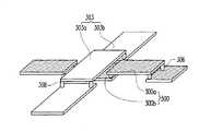
触控电极层203位于第二基板108上。图3是图2的显示面板中的触控电极层的上视示意图。请同时参照图2以及图3,触控电极层203包括多条第一触控电极300、多条第二触控电极303以及多条周边线路310。第一触控电极300沿着第一方向排列。第二触控电极303沿着第二方向排列。在本实施例中,第一、第二方向分别以X和Y方向为例来说明。 The
承上所述,第一触控电极300与第二触控电极电性303绝缘。另外,每一条第一触控电极300以及每一条第二触控电极303会分别与对应的一条周边线路310电性连接。通过周边线路310可以输入及输出信号至第一触控电极300与第二触控电极电性303。此外,第一触控电极300与第二触控电极303的组成材质包括透明导电材料或是金属。在图3的实施例中,第一触控电极300与第二触控电极303的组成材质是透明导电材料。在其它的实施例中,如第一触控电极300与第二触控电极303是采用金属材质,那么在第一触控电极300与第二触控电极303中更包括形成有多个透光开口图案,且每一透光开口图案是对应画素数组103中的每一画素结构设置。 As mentioned above, the
更详细而言,每一条第一触控电极300是由多个第一上层触控电极图案300a以及多个第一下层遮蔽电极图案300b交错排列所构成,且每一第一上层触控电极图案300a与邻接的第一下层遮蔽电极图案300b电性连接。每一条第二触控电极303是由多个第二上层触控电极图案303a以及多个第二下层遮蔽电极图案303b交错排列所构成,且每一第二上层触控电极图案303a与邻接的第二下层遮蔽电极图案303b电性连接。在此,每一个第一上层触控电极图案300a与位于其底下的第二下层触控电极图案303b构成第一触控单元304。每一个第二上层触控电极图案303a与位于其底下的第一下层触控电极图案300b构成第二触控单元305。 In more detail, each
另外,请参照图2,根据本发明的一实施例,第二基板108上更包括设置有一保护层204以及一电极膜205。保护层204覆盖于触控电极层203上。电极膜205位于保护层204上。在另一实施例中,第二基板108上更包括设置有彩色滤光层(未绘示)。彩色滤光层覆盖在触控电极层203上。彩色滤光层例如由绿色滤光层、蓝色滤光层以及红光滤光层所构成。 In addition, referring to FIG. 2 , according to an embodiment of the present invention, the
特别是,在本实施例中,保护层204的加入可增加触控电极层203与电极膜205间的距离,以达到减少寄生电容的电容值。在一实施例中,保护层105的厚度范围为10~50微米 

另外,在本实施例中,每一第一上层触控电极图案300a、每一第一下层遮蔽电极图案300b、每一第二上层触控电极图案303a或每一第二下层遮蔽电极图案303b的面积为一单位触控面积307的1/2~2/3。一般而言,一个单位触控面积307大约为0.5cm×0.5cm,其相当于一个手指头的大小。上述触控电极图案300a、303a的面积的设计主要是为了能够精确的辨识出触控位置,详细说明如下: In addition, in this embodiment, each first upper layer
请继续参照图3,以下以坐标位置(Xn,Yn)来定义第二上层触控电极图案303a与第一下层遮蔽电极图案300b的重叠位置以及第一上层触控电极图案300a与第二下层遮蔽电极图案303b的重叠位置,也就是定义触控单元304、305的位置。举例而言,当手指接触到坐标位置(Xn+2,Yn-1)时,由于第二下层遮蔽电极图案303b被第一上层触控电极图案300a所遮挡,因而在坐标位置Yn-1的第二下层遮蔽电极图案303b无法感应到手指的触控,因而其造成X坐标无法判断。故X坐标必须由靠邻近的坐标位置(Xn+1,Yn-1)或坐标位置(Xn+3,Yn-1)上的第二上层触控电极303a与手指间引发的感应电容来判断。因此,为避免触控电极图案某一方向没有感应位置的效果,每一个触控电极的尺寸不能太大,因此,触控电极层的触控电极图案的面积较佳的是单位触控面积307的1/2~2/3。 Please continue to refer to FIG. 3 , the overlapping position of the second upper layer
以下将以立体图以及剖面图来细部说明本发明的触控电极层。图4为图3的触控电极层的局部立面放大图。请参照图3及图4,在本实施例中,第一上层触控电极图案300a与第二上层触控电极图案303a共平面,而且第一下层遮蔽电极图案300b与第二下层遮蔽电极图案303b共平面。另外,第一上层触控电极图案300a的尺寸与第二下层遮蔽电极图案303b的尺寸实质上相同,且第二上层触控电极图案的尺寸303a与第一下层遮蔽电极图案300b的尺寸实质上相同。此外,本实施例采用多个第一接触结构306以电性连接同一列的第一上层触控电极图案300a和第一下层遮蔽电极图案300b,且采用多个第二接触结构308以电性连接同一行的第二上层触控电极图案303a和第二下层遮蔽电极图案303b。在本实施例中,每一接触结构306、308为两个接触插塞。然而在其它实施例中,接触结构306、308也可以分别是一接触插塞即可,或是三个或三个以上接触插塞(如图5A所示)。此外,接触结构306、308甚至也可以是一连续接触结构,其目的是用来将下两层的电极层做电性连接,其详细整体外观可参照图5B。 The touch electrode layer of the present invention will be described in detail below with perspective views and cross-sectional views. FIG. 4 is an enlarged view of a partial elevation of the touch electrode layer in FIG. 3 . 3 and 4, in this embodiment, the first upper layer
另外,图6A为沿着图3中的I1-I1’剖面线所示的剖面示意图,而图6B为沿着图3中的I2-I2’剖面线所示的剖面示意图。请参照图3以及图6A与图6B,在本实施例中,在第一上层触控电极图案300a与第二下层遮蔽电极图案303b之间更包含一层绝缘层602。在第二上层触控电极图案303a与第一下层遮蔽电极图案300b之间包含一层绝缘层602。而且当于进行触控操作时,彼此重叠的第一上层触控电极图案300a与第二下层遮蔽电极图案303b之间具有相同信号。另外,彼此重叠的第二上层触控电极图案303a与第一下层遮蔽电极图案300b间也具有相同信号。当彼此重叠的两导电层之间具有相同的电位或是电压信号时,两导电层之间即不会存在有寄生电容。本发明的触控电极层的设计方式并使重叠的两电极图案之间具有相同的电压信号,将可以降低触控电极层与电极膜之间所产生的寄生电容。 In addition, FIG. 6A is a schematic cross-sectional view along the line I1 -I1 ′ in FIG. 3 , and FIG. 6B is a schematic cross-sectional view along the line I2 -I2 ′ in FIG. 3 . Referring to FIG. 3 and FIGS. 6A and 6B , in this embodiment, an insulating
更详细而言,请参照图2、图3以及图4,为了减少触控电极层203和电极膜105间的寄生电容,本发明的第一实施例透过将第一触控电极300和第二触控电极303上下交错的排列结构,并使彼此重叠的电极图案具有相同的信号 的方式来达成。换言之,当第一上层触控电极图案300a和第二下层遮蔽电极图案303b被给一相同频率、相同大小的信号时,第一上层触控电极图案300a与第二下层遮蔽电极图案303b间会因信号的相同而不会存在有电容。而且,利用第二下层遮蔽电极图案303b可隔绝第一上层触控电极图案300a与电极膜105间的信号干扰。故此,第一上层触控电极图案300a、第二下层遮蔽电极图案303b、第二上层触控电极303a以及第一下层触控电极图案300b的面积大小相近,可对信号干扰作有效隔绝作用,并达到降低寄生电容的效果。 In more detail, please refer to FIG. 2, FIG. 3 and FIG. The two
第二实施例second embodiment
图7绘示为依照本发明第二实施例的触控电极层的上视示意图。请参照图7,本实施例与图3的实施例的触控电极层203相似,不同之处在于本实施例的触控电极层700分成至少两个区域。在图7中是将触控电极层700分成四个区域A、B、C、D,但本发明不限制区域的数目。 FIG. 7 is a schematic top view of a touch electrode layer according to a second embodiment of the present invention. Referring to FIG. 7 , this embodiment is similar to the
在图7中,区域A内的第一触控电极706和第二触控电极708与其它三个区域B、C、D内的第一触控电极702、716、718及第二触控电极704、720、722绝缘。而且区域A内的每一条第一触控电极706以及每一条第二触控电极708皆分别与一条周边线路712电性连接。类似地,区域B内的第一触控电极702以及第二触控电极704也会与其它区域内的触控电极绝缘,且各区域内的每一条第一触控电极702以及每一条第二触控电极704皆分别与一条周边线路710电性连接。 In FIG. 7 , the
综上所述,本发明将触控电极层内嵌于显示面板内部,其不但可减少面板的整体制程,也可降低了面板的薄化成本。另外,本发明的触控电极层中的第一与第二触控电极是以重叠交错排列方式设置,并使重叠的电极图案具有相同的电压信号,其可降低了触控电极层与电极膜之间的寄生电容,进而增加触控电极层的感应灵敏度。 To sum up, the present invention embeds the touch electrode layer inside the display panel, which not only reduces the overall manufacturing process of the panel, but also reduces the thinning cost of the panel. In addition, the first and second touch electrodes in the touch electrode layer of the present invention are arranged in an overlapping and staggered arrangement, and the overlapping electrode patterns have the same voltage signal, which can reduce the contact between the touch electrode layer and the electrode film. The parasitic capacitance between them increases the sensing sensitivity of the touch electrode layer. the
虽然本发明已以实施例揭露如上,然其并非用以限定本发明,任何所属技术领域中具有通常知识者,在不脱离本发明的精神和范围内,当可作些许的更动与润饰,因此本发明的保护范围当视后附的申请专利范围所界定者为准。Although the present invention has been disclosed as above with the embodiments, it is not intended to limit the present invention. Anyone with ordinary knowledge in the technical field can make some changes and modifications without departing from the spirit and scope of the present invention. Therefore, the scope of protection of the present invention should be defined by the scope of the appended patent application.
Claims (18)
Priority Applications (1)
| Application Number | Priority Date | Filing Date | Title |
|---|---|---|---|
| CN2008101796997ACN101414070B (en) | 2008-12-01 | 2008-12-01 | Touch electrode layer and display panel |
Applications Claiming Priority (1)
| Application Number | Priority Date | Filing Date | Title |
|---|---|---|---|
| CN2008101796997ACN101414070B (en) | 2008-12-01 | 2008-12-01 | Touch electrode layer and display panel |
Publications (2)
| Publication Number | Publication Date |
|---|---|
| CN101414070A CN101414070A (en) | 2009-04-22 |
| CN101414070Btrue CN101414070B (en) | 2011-03-23 |
Family
ID=40594683
Family Applications (1)
| Application Number | Title | Priority Date | Filing Date |
|---|---|---|---|
| CN2008101796997AActiveCN101414070B (en) | 2008-12-01 | 2008-12-01 | Touch electrode layer and display panel |
Country Status (1)
| Country | Link |
|---|---|
| CN (1) | CN101414070B (en) |
Cited By (1)
| Publication number | Priority date | Publication date | Assignee | Title |
|---|---|---|---|---|
| US11360602B2 (en) | 2017-05-26 | 2022-06-14 | Boe Technology Group Co., Ltd. | Display device, touch display panel and driving method thereof |
Families Citing this family (11)
| Publication number | Priority date | Publication date | Assignee | Title |
|---|---|---|---|---|
| CN101872272A (en) | 2009-04-23 | 2010-10-27 | 联想(北京)有限公司 | Surface capacitance type touch screen and electronic equipment |
| CN101719037B (en)* | 2009-12-30 | 2011-06-01 | 友达光电股份有限公司 | touch display panel |
| CN101882040B (en)* | 2010-03-12 | 2012-12-19 | 敦泰科技有限公司 | Mutually capacitive touch screen with electrodes arranged on double-layer conductive material thin film |
| TWI463362B (en)* | 2011-07-28 | 2014-12-01 | Tpk Touch Solutions Inc | Touch display device and method of manufacturing same |
| CN102360260A (en)* | 2011-10-27 | 2012-02-22 | 汕头超声显示器(二厂)有限公司 | Sensing electrode for projection type capacitance touch screen |
| CN103092450B (en)* | 2013-01-28 | 2016-09-07 | 北京京东方光电科技有限公司 | A kind of touch-screen and manufacture method, display device |
| CN105549798A (en)* | 2014-10-30 | 2016-05-04 | 中强光电股份有限公司 | Touch projection screen and projection system using same |
| CN106293231B (en)* | 2016-08-11 | 2024-03-12 | 厦门天马微电子有限公司 | Touch display panel and display device |
| CN108614652B (en)* | 2016-12-13 | 2021-07-09 | 和鑫光电股份有限公司 | touch panel |
| CN107783699B (en)* | 2017-10-16 | 2021-05-04 | 业成科技(成都)有限公司 | Touch panel structure and manufacturing method thereof |
| CN110277072B (en)* | 2018-03-15 | 2020-07-28 | 北京京东方光电科技有限公司 | Common electrode voltage compensation method, device and touch display module |
- 2008
- 2008-12-01CNCN2008101796997Apatent/CN101414070B/enactiveActive
Cited By (1)
| Publication number | Priority date | Publication date | Assignee | Title |
|---|---|---|---|---|
| US11360602B2 (en) | 2017-05-26 | 2022-06-14 | Boe Technology Group Co., Ltd. | Display device, touch display panel and driving method thereof |
Also Published As
| Publication number | Publication date |
|---|---|
| CN101414070A (en) | 2009-04-22 |
Similar Documents
| Publication | Publication Date | Title |
|---|---|---|
| CN101414070B (en) | Touch electrode layer and display panel | |
| CN103176674B (en) | Touch panel and touch display panel | |
| US9372360B2 (en) | Touch liquid crystal display device | |
| JP3154829U (en) | IPS liquid crystal display with touch function | |
| US9091874B2 (en) | Touch control liquid crystal display device | |
| KR101564332B1 (en) | Touch screen panel integrated into a liquid crystal display, manufacturing method thereof, and touch sensing method | |
| CN103135292B (en) | There is the LCD device of touch panel | |
| TWI376627B (en) | Sensing electrode layer and display panel | |
| CN102445800B (en) | Liquid crystal display device | |
| CN102341774B (en) | Integrated touch screen | |
| GB2562899B (en) | In-cell touch liquid crystal panels and the array substrates thereof | |
| TWI467297B (en) | Liquid crystal display device | |
| KR101295533B1 (en) | Liquid crystal display device and Method for manufacturing the same | |
| CN102566174B (en) | Liquid crystal display device | |
| KR101758756B1 (en) | Touch sensor, in-cell touch liquid crystal display panel and liquid crystal display | |
| CN106226961B (en) | A COA array substrate and display device | |
| US20140240286A1 (en) | Integrated touch panel for a tft display | |
| CN205176819U (en) | Embedded touch panel | |
| US8730206B2 (en) | Display device including a touch sensor | |
| TWM514052U (en) | In-cell mutual-capacitive touch panel | |
| CN103197463A (en) | Color film substrate and production method, touch screen and display device thereof | |
| US9865201B2 (en) | Pixel structure, display panel, display device and method of fabricating the pixel structure | |
| KR101738570B1 (en) | Liquid crystal display device having touch sensing function | |
| CN105487701A (en) | Touch panel | |
| CN203117609U (en) | Color film substrate, touch screen and display device |
Legal Events
| Date | Code | Title | Description |
|---|---|---|---|
| C06 | Publication | ||
| PB01 | Publication | ||
| C10 | Entry into substantive examination | ||
| SE01 | Entry into force of request for substantive examination | ||
| C14 | Grant of patent or utility model | ||
| GR01 | Patent grant |