CN101410977A - Semiconductor wafer with high thermal conductivity - Google Patents
Semiconductor wafer with high thermal conductivityDownload PDFInfo
- Publication number
- CN101410977A CN101410977ACNA200780011360XACN200780011360ACN101410977ACN 101410977 ACN101410977 ACN 101410977ACN A200780011360X ACNA200780011360X ACN A200780011360XACN 200780011360 ACN200780011360 ACN 200780011360ACN 101410977 ACN101410977 ACN 101410977A
- Authority
- CN
- China
- Prior art keywords
- carriers
- substrate
- doped
- protective layer
- concentration
- Prior art date
- Legal status (The legal status is an assumption and is not a legal conclusion. Google has not performed a legal analysis and makes no representation as to the accuracy of the status listed.)
- Pending
Links
- 239000004065semiconductorSubstances0.000titleclaimsabstractdescription78
- 239000000758substrateSubstances0.000claimsabstractdescription124
- 239000010410layerSubstances0.000claimsabstractdescription99
- 239000011241protective layerSubstances0.000claimsabstractdescription79
- XUIMIQQOPSSXEZ-UHFFFAOYSA-NSiliconChemical compound[Si]XUIMIQQOPSSXEZ-UHFFFAOYSA-N0.000claimsabstractdescription65
- 229910052710siliconInorganic materials0.000claimsabstractdescription57
- 239000010703siliconSubstances0.000claimsabstractdescription57
- 238000000034methodMethods0.000claimsabstractdescription41
- 239000000969carrierSubstances0.000claimsdescription92
- 239000002019doping agentSubstances0.000claimsdescription66
- WGTYBPLFGIVFAS-UHFFFAOYSA-Mtetramethylammonium hydroxideChemical compound[OH-].C[N+](C)(C)CWGTYBPLFGIVFAS-UHFFFAOYSA-M0.000claimsdescription10
- HEMHJVSKTPXQMS-UHFFFAOYSA-MSodium hydroxideChemical compound[OH-].[Na+]HEMHJVSKTPXQMS-UHFFFAOYSA-M0.000claimsdescription9
- ZOXJGFHDIHLPTG-UHFFFAOYSA-NBoronChemical compound[B]ZOXJGFHDIHLPTG-UHFFFAOYSA-N0.000claimsdescription8
- 229910052796boronInorganic materials0.000claimsdescription8
- QTBSBXVTEAMEQO-UHFFFAOYSA-NAcetic acidChemical compoundCC(O)=OQTBSBXVTEAMEQO-UHFFFAOYSA-N0.000claimsdescription6
- 238000005530etchingMethods0.000claimsdescription6
- 230000002378acidificating effectEffects0.000claimsdescription5
- KRHYYFGTRYWZRS-UHFFFAOYSA-NFluoraneChemical compoundFKRHYYFGTRYWZRS-UHFFFAOYSA-N0.000claimsdescription4
- KWYUFKZDYYNOTN-UHFFFAOYSA-MPotassium hydroxideChemical compound[OH-].[K+]KWYUFKZDYYNOTN-UHFFFAOYSA-M0.000claimsdescription4
- GRYLNZFGIOXLOG-UHFFFAOYSA-NNitric acidChemical compoundO[N+]([O-])=OGRYLNZFGIOXLOG-UHFFFAOYSA-N0.000claimsdescription2
- 150000001875compoundsChemical class0.000claimsdescription2
- 229910017604nitric acidInorganic materials0.000claimsdescription2
- 230000002093peripheral effectEffects0.000claims3
- 150000002500ionsChemical class0.000claims1
- 230000008569processEffects0.000abstractdescription6
- 230000007246mechanismEffects0.000abstractdescription5
- 238000012546transferMethods0.000abstractdescription5
- 230000005855radiationEffects0.000abstractdescription2
- 235000012431wafersNutrition0.000description83
- 239000000463materialSubstances0.000description20
- 238000005286illuminationMethods0.000description10
- 238000010438heat treatmentMethods0.000description9
- 238000010586diagramMethods0.000description7
- 230000017525heat dissipationEffects0.000description7
- 229910021421monocrystalline siliconInorganic materials0.000description7
- 238000005516engineering processMethods0.000description6
- 230000000694effectsEffects0.000description5
- 230000005684electric fieldEffects0.000description5
- 238000004519manufacturing processMethods0.000description5
- 230000007704transitionEffects0.000description5
- 238000009792diffusion processMethods0.000description4
- 239000002210silicon-based materialSubstances0.000description4
- QVGXLLKOCUKJST-UHFFFAOYSA-Natomic oxygenChemical compound[O]QVGXLLKOCUKJST-UHFFFAOYSA-N0.000description3
- 230000008901benefitEffects0.000description3
- 239000002800charge carrierSubstances0.000description3
- 230000007423decreaseEffects0.000description3
- 238000000151depositionMethods0.000description3
- 238000013461designMethods0.000description3
- 238000009826distributionMethods0.000description3
- 239000007789gasSubstances0.000description3
- 238000005468ion implantationMethods0.000description3
- 229910052760oxygenInorganic materials0.000description3
- 239000001301oxygenSubstances0.000description3
- 229910052698phosphorusInorganic materials0.000description3
- 238000005498polishingMethods0.000description3
- 239000000126substanceSubstances0.000description3
- OAICVXFJPJFONN-UHFFFAOYSA-NPhosphorusChemical compound[P]OAICVXFJPJFONN-UHFFFAOYSA-N0.000description2
- 238000005229chemical vapour depositionMethods0.000description2
- 239000013078crystalSubstances0.000description2
- 230000008021depositionEffects0.000description2
- 230000006872improvementEffects0.000description2
- 238000005259measurementMethods0.000description2
- 238000001465metallisationMethods0.000description2
- 238000004377microelectronicMethods0.000description2
- 230000000737periodic effectEffects0.000description2
- 239000011574phosphorusSubstances0.000description2
- 238000004088simulationMethods0.000description2
- 239000007858starting materialSubstances0.000description2
- 239000012808vapor phaseSubstances0.000description2
- 238000004857zone meltingMethods0.000description2
- 108091006149Electron carriersProteins0.000description1
- GYHNNYVSQQEPJS-UHFFFAOYSA-NGalliumChemical compound[Ga]GYHNNYVSQQEPJS-UHFFFAOYSA-N0.000description1
- 230000002776aggregationEffects0.000description1
- 238000004220aggregationMethods0.000description1
- 229910052782aluminiumInorganic materials0.000description1
- XAGFODPZIPBFFR-UHFFFAOYSA-NaluminiumChemical compound[Al]XAGFODPZIPBFFR-UHFFFAOYSA-N0.000description1
- 239000006117anti-reflective coatingSubstances0.000description1
- 229910052787antimonyInorganic materials0.000description1
- WATWJIUSRGPENY-UHFFFAOYSA-Nantimony atomChemical compound[Sb]WATWJIUSRGPENY-UHFFFAOYSA-N0.000description1
- 238000013459approachMethods0.000description1
- 238000000149argon plasma sinteringMethods0.000description1
- 229910052785arsenicInorganic materials0.000description1
- RQNWIZPPADIBDY-UHFFFAOYSA-Narsenic atomChemical compound[As]RQNWIZPPADIBDY-UHFFFAOYSA-N0.000description1
- 239000012159carrier gasSubstances0.000description1
- 238000003486chemical etchingMethods0.000description1
- 238000002109crystal growth methodMethods0.000description1
- 238000001978electrochemical passivationMethods0.000description1
- 238000005538encapsulationMethods0.000description1
- 230000006870functionEffects0.000description1
- 229910052733galliumInorganic materials0.000description1
- 238000000227grindingMethods0.000description1
- BHEPBYXIRTUNPN-UHFFFAOYSA-Nhydridophosphorus(.) (triplet)Chemical compound[PH]BHEPBYXIRTUNPN-UHFFFAOYSA-N0.000description1
- 229910052738indiumInorganic materials0.000description1
- APFVFJFRJDLVQX-UHFFFAOYSA-Nindium atomChemical compound[In]APFVFJFRJDLVQX-UHFFFAOYSA-N0.000description1
- 230000010354integrationEffects0.000description1
- -1interconnectsSubstances0.000description1
- 229910052751metalInorganic materials0.000description1
- 239000002184metalSubstances0.000description1
- 230000005012migrationEffects0.000description1
- 238000013508migrationMethods0.000description1
- 238000012986modificationMethods0.000description1
- 230000004048modificationEffects0.000description1
- 229910052757nitrogenInorganic materials0.000description1
- 230000005693optoelectronicsEffects0.000description1
- 239000005022packaging materialSubstances0.000description1
- 238000004806packaging method and processMethods0.000description1
- 230000003071parasitic effectEffects0.000description1
- 239000012071phaseSubstances0.000description1
- 230000002265preventionEffects0.000description1
- 238000012545processingMethods0.000description1
- 230000009993protective functionEffects0.000description1
- 230000000191radiation effectEffects0.000description1
- 230000006798recombinationEffects0.000description1
- 238000005215recombinationMethods0.000description1
- 230000009467reductionEffects0.000description1
- 230000001568sexual effectEffects0.000description1
- 150000003377silicon compoundsChemical class0.000description1
- 239000002356single layerSubstances0.000description1
- 238000010561standard procedureMethods0.000description1
- 238000012876topographyMethods0.000description1
- 230000001052transient effectEffects0.000description1
Images


Classifications
- H—ELECTRICITY
- H01—ELECTRIC ELEMENTS
- H01L—SEMICONDUCTOR DEVICES NOT COVERED BY CLASS H10
- H01L21/00—Processes or apparatus adapted for the manufacture or treatment of semiconductor or solid state devices or of parts thereof
- H01L21/02—Manufacture or treatment of semiconductor devices or of parts thereof
- H01L21/04—Manufacture or treatment of semiconductor devices or of parts thereof the devices having potential barriers, e.g. a PN junction, depletion layer or carrier concentration layer
- H01L21/18—Manufacture or treatment of semiconductor devices or of parts thereof the devices having potential barriers, e.g. a PN junction, depletion layer or carrier concentration layer the devices having semiconductor bodies comprising elements of Group IV of the Periodic Table or AIIIBV compounds with or without impurities, e.g. doping materials
- H01L21/30—Treatment of semiconductor bodies using processes or apparatus not provided for in groups H01L21/20 - H01L21/26
- H01L21/302—Treatment of semiconductor bodies using processes or apparatus not provided for in groups H01L21/20 - H01L21/26 to change their surface-physical characteristics or shape, e.g. etching, polishing, cutting
- H01L21/306—Chemical or electrical treatment, e.g. electrolytic etching
- H01L21/30604—Chemical etching
- H01L21/30608—Anisotropic liquid etching
- H—ELECTRICITY
- H01—ELECTRIC ELEMENTS
- H01L—SEMICONDUCTOR DEVICES NOT COVERED BY CLASS H10
- H01L21/00—Processes or apparatus adapted for the manufacture or treatment of semiconductor or solid state devices or of parts thereof
- H01L21/02—Manufacture or treatment of semiconductor devices or of parts thereof
- H01L21/04—Manufacture or treatment of semiconductor devices or of parts thereof the devices having potential barriers, e.g. a PN junction, depletion layer or carrier concentration layer
- H01L21/18—Manufacture or treatment of semiconductor devices or of parts thereof the devices having potential barriers, e.g. a PN junction, depletion layer or carrier concentration layer the devices having semiconductor bodies comprising elements of Group IV of the Periodic Table or AIIIBV compounds with or without impurities, e.g. doping materials
- H01L21/22—Diffusion of impurity materials, e.g. doping materials, electrode materials, into or out of a semiconductor body, or between semiconductor regions; Interactions between two or more impurities; Redistribution of impurities
- H—ELECTRICITY
- H01—ELECTRIC ELEMENTS
- H01L—SEMICONDUCTOR DEVICES NOT COVERED BY CLASS H10
- H01L21/00—Processes or apparatus adapted for the manufacture or treatment of semiconductor or solid state devices or of parts thereof
- H01L21/02—Manufacture or treatment of semiconductor devices or of parts thereof
- H01L21/02104—Forming layers
- H01L21/02365—Forming inorganic semiconducting materials on a substrate
- H01L21/02367—Substrates
- H01L21/0237—Materials
- H01L21/02373—Group 14 semiconducting materials
- H01L21/02381—Silicon, silicon germanium, germanium
- H—ELECTRICITY
- H01—ELECTRIC ELEMENTS
- H01L—SEMICONDUCTOR DEVICES NOT COVERED BY CLASS H10
- H01L21/00—Processes or apparatus adapted for the manufacture or treatment of semiconductor or solid state devices or of parts thereof
- H01L21/02—Manufacture or treatment of semiconductor devices or of parts thereof
- H01L21/02104—Forming layers
- H01L21/02365—Forming inorganic semiconducting materials on a substrate
- H01L21/02436—Intermediate layers between substrates and deposited layers
- H01L21/02439—Materials
- H01L21/02441—Group 14 semiconducting materials
- H01L21/0245—Silicon, silicon germanium, germanium
- H—ELECTRICITY
- H01—ELECTRIC ELEMENTS
- H01L—SEMICONDUCTOR DEVICES NOT COVERED BY CLASS H10
- H01L21/00—Processes or apparatus adapted for the manufacture or treatment of semiconductor or solid state devices or of parts thereof
- H01L21/02—Manufacture or treatment of semiconductor devices or of parts thereof
- H01L21/02104—Forming layers
- H01L21/02365—Forming inorganic semiconducting materials on a substrate
- H01L21/02518—Deposited layers
- H01L21/02521—Materials
- H01L21/02524—Group 14 semiconducting materials
- H01L21/02532—Silicon, silicon germanium, germanium
- H—ELECTRICITY
- H10—SEMICONDUCTOR DEVICES; ELECTRIC SOLID-STATE DEVICES NOT OTHERWISE PROVIDED FOR
- H10D—INORGANIC ELECTRIC SEMICONDUCTOR DEVICES
- H10D62/00—Semiconductor bodies, or regions thereof, of devices having potential barriers
- H—ELECTRICITY
- H10—SEMICONDUCTOR DEVICES; ELECTRIC SOLID-STATE DEVICES NOT OTHERWISE PROVIDED FOR
- H10D—INORGANIC ELECTRIC SEMICONDUCTOR DEVICES
- H10D62/00—Semiconductor bodies, or regions thereof, of devices having potential barriers
- H10D62/60—Impurity distributions or concentrations
- H—ELECTRICITY
- H10—SEMICONDUCTOR DEVICES; ELECTRIC SOLID-STATE DEVICES NOT OTHERWISE PROVIDED FOR
- H10F—INORGANIC SEMICONDUCTOR DEVICES SENSITIVE TO INFRARED RADIATION, LIGHT, ELECTROMAGNETIC RADIATION OF SHORTER WAVELENGTH OR CORPUSCULAR RADIATION
- H10F39/00—Integrated devices, or assemblies of multiple devices, comprising at least one element covered by group H10F30/00, e.g. radiation detectors comprising photodiode arrays
- H10F39/10—Integrated devices
- H10F39/12—Image sensors
- H10F39/199—Back-illuminated image sensors
- H—ELECTRICITY
- H01—ELECTRIC ELEMENTS
- H01L—SEMICONDUCTOR DEVICES NOT COVERED BY CLASS H10
- H01L21/00—Processes or apparatus adapted for the manufacture or treatment of semiconductor or solid state devices or of parts thereof
- H01L21/02—Manufacture or treatment of semiconductor devices or of parts thereof
- H01L21/04—Manufacture or treatment of semiconductor devices or of parts thereof the devices having potential barriers, e.g. a PN junction, depletion layer or carrier concentration layer
- H01L21/18—Manufacture or treatment of semiconductor devices or of parts thereof the devices having potential barriers, e.g. a PN junction, depletion layer or carrier concentration layer the devices having semiconductor bodies comprising elements of Group IV of the Periodic Table or AIIIBV compounds with or without impurities, e.g. doping materials
- H01L21/22—Diffusion of impurity materials, e.g. doping materials, electrode materials, into or out of a semiconductor body, or between semiconductor regions; Interactions between two or more impurities; Redistribution of impurities
- H01L21/225—Diffusion of impurity materials, e.g. doping materials, electrode materials, into or out of a semiconductor body, or between semiconductor regions; Interactions between two or more impurities; Redistribution of impurities using diffusion into or out of a solid from or into a solid phase, e.g. a doped oxide layer
- H01L21/2251—Diffusion into or out of group IV semiconductors
- H01L21/2252—Diffusion into or out of group IV semiconductors using predeposition of impurities into the semiconductor surface, e.g. from a gaseous phase
- H01L21/2253—Diffusion into or out of group IV semiconductors using predeposition of impurities into the semiconductor surface, e.g. from a gaseous phase by ion implantation
- H—ELECTRICITY
- H10—SEMICONDUCTOR DEVICES; ELECTRIC SOLID-STATE DEVICES NOT OTHERWISE PROVIDED FOR
- H10F—INORGANIC SEMICONDUCTOR DEVICES SENSITIVE TO INFRARED RADIATION, LIGHT, ELECTROMAGNETIC RADIATION OF SHORTER WAVELENGTH OR CORPUSCULAR RADIATION
- H10F39/00—Integrated devices, or assemblies of multiple devices, comprising at least one element covered by group H10F30/00, e.g. radiation detectors comprising photodiode arrays
- H10F39/80—Constructional details of image sensors
- H—ELECTRICITY
- H10—SEMICONDUCTOR DEVICES; ELECTRIC SOLID-STATE DEVICES NOT OTHERWISE PROVIDED FOR
- H10F—INORGANIC SEMICONDUCTOR DEVICES SENSITIVE TO INFRARED RADIATION, LIGHT, ELECTROMAGNETIC RADIATION OF SHORTER WAVELENGTH OR CORPUSCULAR RADIATION
- H10F77/00—Constructional details of devices covered by this subclass
- H10F77/10—Semiconductor bodies
- H10F77/14—Shape of semiconductor bodies; Shapes, relative sizes or dispositions of semiconductor regions within semiconductor bodies
- H10F77/148—Shapes of potential barriers
Landscapes
- Engineering & Computer Science (AREA)
- Microelectronics & Electronic Packaging (AREA)
- Condensed Matter Physics & Semiconductors (AREA)
- General Physics & Mathematics (AREA)
- Manufacturing & Machinery (AREA)
- Computer Hardware Design (AREA)
- Physics & Mathematics (AREA)
- Power Engineering (AREA)
- Chemical & Material Sciences (AREA)
- Chemical Kinetics & Catalysis (AREA)
- General Chemical & Material Sciences (AREA)
- Materials Engineering (AREA)
- Recrystallisation Techniques (AREA)
- Crystals, And After-Treatments Of Crystals (AREA)
Abstract
Description
Translated fromChinese技术领域technical field
本发明一般涉及一种半导体晶片及其制造方法。更具体地,本发明涉及一种半导体晶片,其具有改善的热导率特性,当用作高速处理器器件的衬底时提供优势。The present invention generally relates to a semiconductor wafer and a method of manufacturing the same. More specifically, the present invention relates to a semiconductor wafer having improved thermal conductivity characteristics that provide advantages when used as a substrate for a high speed processor device.
背景技术Background technique
在半导体产业内,总的按比例缩放趋势已经通过增加晶体管密度和处理器器件上的操作频率而增加硅功率密度。然而,从设计和工艺改进获得的功率减小不足以补偿伴随增加的功率密度的较高操作温度。而且,在较高操作温度下,半导体的电性能和可靠性明显地退化,降低了半导体处理器的速度和寿命。同样地,降低跨过该结构的半导体结温日益重要,特别是避免在较高功率密度下运行的区域中的局部热斑。Within the semiconductor industry, the general scaling trend has increased silicon power density by increasing transistor density and operating frequency on processor devices. However, the power reductions obtained from design and process improvements are insufficient to compensate for the higher operating temperatures that accompany increased power densities. Furthermore, at higher operating temperatures, the electrical performance and reliability of semiconductors degrade significantly, reducing the speed and lifetime of semiconductor processors. Likewise, reducing the semiconductor junction temperature across the structure is increasingly important, especially to avoid localized hot spots in regions operating at higher power densities.
目前,大多数高性能处理器器件制造在薄(约2-4μm)的、轻掺杂(约1×10¹⁵-1×10¹⁶载流子/cm3)的外延硅层上,该外延硅层生长在重掺杂(约1019载流子/cm3)的硅衬底晶片之上,其中优选硼作为掺杂剂。这种类型的晶片通常称作P/P++外延晶片或P/P+外延晶片。诸如这些的外延硅层典型地通过化学气相沉积工艺生长,其中在气态的硅化合物从该晶片表面经过的同时加热衬底以发生热解或分解。At present, most high-performance processor devices are fabricated on thin (about 2-4 μm), lightly doped (about 1×10¹⁵ -1×10¹⁶ carriers/cm3 ) epitaxial silicon layer, the epitaxial silicon The layers are grown on heavily doped (about 1019 carriers/cm3 ) silicon substrate wafers, with boron being preferred as dopant. This type of wafer is commonly referred to as a P/P++ epitaxial wafer or a P/P+ epitaxial wafer. Epitaxial silicon layers such as these are typically grown by chemical vapor deposition processes in which the substrate is heated to pyrolyze or decompose while gaseous silicon compounds are passed across the wafer surface.
在器件层之下的重掺杂硅衬底旨在提供保护,以免遭受多种常见的器件失效机理,例如器件闩锁失效、与扩散泄漏电流有关的失效或一些与辐射效应有关的失效。例如,闩锁失效指的是一种在寄生结处导致完全短路的电子聚集现象,但是可以使用特别是关键掺杂设计来避免闩锁失效。因此,在重掺杂硅衬底上的轻掺杂器件层的设置提供理想的闩锁和低扩散电流特性。The heavily doped silicon substrate below the device layer is intended to provide protection from several common device failure mechanisms such as device latch-up failures, failures related to diffusion leakage currents, or some failures related to radiation effects. For example, latch-up failure refers to a phenomenon of electron build-up that leads to a dead short at a parasitic junction, but latch-up failure can be avoided using especially critical doping designs. Thus, the placement of lightly doped device layers on heavily doped silicon substrates provides desirable latch-up and low diffusion current characteristics.
使用重掺杂硅衬底的一个缺点是其与轻掺杂器件层相比的差的导热性;据报导,轻掺杂硅的热导率比重掺杂硅的热导率高约20%,且可能更高。例如参见P.Komarov et al.,Transient Thermo-ReflectanceMeasurements of the Thermal Conductivity and Interface Resistance ofMetallized Natural and Isotopically-Pure Silicon,34 MicroelectronicsJournal No.12,1115-1118页(2003)。热导率的差异是显著的,这是因为在薄器件层中产生的热量的大部分借由通过硅衬底的散逸而传递到周围环境,且较小的热导率倾向于降低效率和可靠性。One disadvantage of using heavily doped silicon substrates is its poor thermal conductivity compared to lightly doped device layers; the thermal conductivity of lightly doped silicon has been reported to be about 20% higher than that of heavily doped silicon, and possibly higher. See, eg, P. Komarov et al., Transient Thermo-Reflectance Measurements of the Thermal Conductivity and Interface Resistance of Metallized Natural and Isotopically-Pure Silicon, 34 Microelectronics Journal No. 12, pp. 1115-1118 (2003). The difference in thermal conductivity is significant because most of the heat generated in thin device layers is transferred to the surrounding environment by dissipation through the silicon substrate, and smaller thermal conductivities tend to reduce efficiency and reliability. sex.
为了改善从器件层的排热,以前的努力集中在改善使用期间从硅衬底背面经由封装(packaging)向外界的热传递特性。虽然封装材料的设计和热沉已经降低了在该界面处的热阻以保持较低的芯片温度,这种努力没有解决器件层中在热斑处的局部加热的问题。To improve heat removal from the device layers, previous efforts have focused on improving the heat transfer characteristics from the backside of the silicon substrate via packaging to the outside world during use. While the design of packaging materials and heat sinks have reduced the thermal resistance at this interface to maintain lower chip temperatures, such efforts have not addressed the problem of localized heating at hot spots in the device layers.
当重掺杂衬底与轻掺杂器件层集成时,另一个普遍遇到的问题是背面自动掺杂,即,掺杂剂原子从衬底的背部或侧面向器件层中的移动。限制这种效应的一个常规手段是在高掺杂衬底上形成背面氧化密封。然而,在双面抛光的晶片的情况下,该氧化密封不能集成到外延硅结构中。Another commonly encountered problem when integrating heavily doped substrates with lightly doped device layers is backside autodoping, ie, the movement of dopant atoms from the back or sides of the substrate into the device layers. One conventional means of limiting this effect is to form a backside oxide seal on the highly doped substrate. However, in the case of double-sided polished wafers, this oxide seal cannot be integrated into epitaxial silicon structures.
当将具有轻掺杂外延层的重掺杂衬底用于其中希望有背面照明技术的CMOS图像传感器应用中时,还提出了挑战。当前,商业可用的图像传感器是从器件侧照明的。对于典型的器件侧照明的应用,CMOS图像传感器硅晶片包括被掺杂到P+或P++浓度的衬底以及被掺杂到P浓度的外延层。器件侧照明的公知应用不能满足按比例缩放趋势和在这种应用中的目标,其包括通过先进的金属互连而减小了象素尺寸且提高了电路的功能性。相信背面照明可以实现这些目标,同时还提高器件的填充因数和量子效率。这些条件被用作测量实际上能够照明图像传感器的光能的净额的不同方式。填充因数,其指的是图像传感器的能够暴露于光的百分比或部分,在传统的器件侧照明器件中,由于日益复杂的金属化层和膜以及先进的器件形貌而被降低了。随着填充因数的降低,衡量投射光能够产生活性电子载流子的效率如何的量子效率也降低了。Challenges are also presented when heavily doped substrates with lightly doped epitaxial layers are used in CMOS image sensor applications where backside illumination technology is desired. Currently, commercially available image sensors are illuminated from the device side. For typical device-side illumination applications, a CMOS image sensor silicon wafer includes a substrate doped to a P+ or P++ concentration and an epitaxial layer doped to a P concentration. Known applications of device-side illumination do not meet scaling trends and goals in such applications, which include reduced pixel size and increased circuit functionality through advanced metal interconnects. It is believed that backside illumination can achieve these goals while also improving the fill factor and quantum efficiency of the device. These conditions are used as different ways of measuring the net amount of light energy that can actually illuminate the image sensor. Fill factor, which refers to the percentage or portion of an image sensor that can be exposed to light, is reduced in conventional device-side illuminated devices due to increasingly complex metallization layers and films and advanced device topography. As the fill factor decreases, the quantum efficiency, which measures how efficiently the projected light is able to generate active electron carriers, also decreases.
使用背面照明技术可以使这些所期望的对图像传感器性能的改进成为可能,这是因为器件侧的特征,例如器件图形、金属化层、互连和膜不会妨碍照明过程。结果是接近100%的填充因数、改进的抗反射涂层的灵活性以及增加了的量子效率。而且,背面照明允许先进的器件体系结构和互连的集成。然而,背面照明必须在器件侧光电二极管的几个微米内执行,以将可见光有效地转换成电信号。这就需要从原始的所形成的硅结构的背面一致地且均匀地去除材料,以产生光滑的背面表面,其要求所述硅结构从几百微米减薄到仅几个微米,例如小于约15μm。而且,背面表面必须能够被钝化,防止在所述表面处的光生载流子的复合,同时还能利用在图像传感器器件内的电场,将这些光生载流子引导至收集光电二极管。使用常规的机械或化学手段来减薄所述硅结构不容易得到这些特征。在这样小的尺寸下,机械的减薄手段是不可行的,同时在图像传感器的物理特征的容差内控制化学去除率也是困难的。These desired improvements to image sensor performance are made possible using backside illumination technology because device-side features such as device patterns, metallization layers, interconnects, and films do not interfere with the illumination process. The result is a fill factor approaching 100%, improved flexibility of the anti-reflective coating, and increased quantum efficiency. Furthermore, backside illumination allows integration of advanced device architectures and interconnects. However, backside illumination must be performed within a few micrometers of the device-side photodiodes to efficiently convert visible light into electrical signals. This requires consistent and uniform removal of material from the backside of the original as-formed silicon structure to produce a smooth backside surface, which requires thinning of the silicon structure from a few hundred microns to only a few microns, for example less than about 15 μm . Furthermore, the backside surface must be able to be passivated, preventing recombination of photogenerated carriers at the surface, while still utilizing the electric field within the image sensor device to direct these photogenerated carriers to the collecting photodiodes. These features are not readily achievable using conventional mechanical or chemical means to thin the silicon structure. At such small sizes, mechanical thinning approaches are not feasible, while controlling the chemical removal rate within the tolerances of the image sensor's physical characteristics is also difficult.
发明内容Contents of the invention
在本发明的不同方面中,提供一种硅半导体晶片,其具有良好的热传递特性,同时提供对常见的半导体失效机理的抵抗力。In various aspects of the invention, a silicon semiconductor wafer is provided that has good heat transfer characteristics while providing resistance to common semiconductor failure mechanisms.
因此,简而言之,本发明旨在一种半导体晶片,其包括硅器件层、衬底以及硅保护层,所述硅保护层设置在所述器件层和所述衬底之间。所述衬底具有中心轴、通常垂直于所述中心轴的前表面和后表面、圆周边缘、以及从所述中心轴延伸到所述圆周边缘的半径。所述保护层具有至少约0.5μm的厚度且被掺杂,所述保护层中的掺杂剂的浓度在约6.0×10¹⁷载流子/cm3和约1.0×1020载流子/cm3之间。所述衬底和所述器件层也被掺杂,其中所述衬底和器件层中的掺杂剂浓度小于约1.0×1017载流子/cm3。Thus, in brief, the present invention is directed to a semiconductor wafer comprising a silicon device layer, a substrate and a silicon protective layer disposed between said device layer and said substrate. The substrate has a central axis, front and rear surfaces generally perpendicular to the central axis, a circumferential edge, and a radius extending from the central axis to the circumferential edge. The protective layer has a thickness of at least about 0.5 μm and is doped, the dopant in the protective layer having a concentration between about 6.0×10¹⁷ carriers/cm3 and about 1.0×10²⁰ carriers/cm3 between. The substrate and the device layer are also doped, wherein the dopant concentration in the substrate and device layer is less than about 1.0×10¹⁷ carriers/cm3 .
本发明还旨在一种制备这种半导体晶片的方法。The invention is also directed to a method of producing such a semiconductor wafer.
其它目的和特征将在下文中部分地明显和部分地指出。Other objects and features will be in part apparent and in part pointed out hereinafter.
附图说明Description of drawings
图1是本发明的半导体晶片的示意性截面图。Fig. 1 is a schematic cross-sectional view of a semiconductor wafer of the present invention.
图2是本发明的半导体晶片自顶而下的示意图,其中图2中的轴与图1中的轴一致。FIG. 2 is a top-down schematic diagram of the semiconductor wafer of the present invention, wherein the axis in FIG. 2 is consistent with the axis in FIG. 1 .
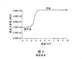
图3是具有高掺杂保护层和轻掺杂衬底的半导体晶片的载流子浓度分布的图示。3 is a graphical representation of the carrier concentration distribution of a semiconductor wafer with a heavily doped protective layer and a lightly doped substrate.
图4是在实例1中详细描述的具有轻掺杂器件层和高掺杂衬底的半导体晶片的载流子浓度分布的图示。4 is a graphical representation of the carrier concentration profile of a semiconductor wafer having a lightly doped device layer and a heavily doped substrate detailed in Example 1. FIG.
图5是具有高掺杂衬底的250μm半导体晶片的局部加热下的散热热图表。Fig. 5 is a thermal graph of heat dissipation under localized heating of a 250 μm semiconductor wafer with a highly doped substrate.
图6是具有高掺杂保护层和轻掺杂衬底的250μm半导体晶片的局部加热下的散热热图表。Fig. 6 is a thermal diagram of heat dissipation under local heating of a 250 μm semiconductor wafer with a highly doped protective layer and a lightly doped substrate.
图7是具有高掺杂衬底的500μm半导体晶片的局部加热下的散热热图表。Fig. 7 is a thermal graph of heat dissipation under localized heating of a 500 μm semiconductor wafer with a highly doped substrate.
图8是具有高掺杂保护层和轻掺杂衬底的500μm半导体晶片的局部加热下的散热热图表。Fig. 8 is a thermal diagram of heat dissipation under local heating of a 500 μm semiconductor wafer with a highly doped protective layer and a lightly doped substrate.
图9是示出在实例2中详细描述的多个半导体结构随着温度变化的热导率的曲线图。FIG. 9 is a graph showing thermal conductivity as a function of temperature for various semiconductor structures detailed in Example 2. FIG.
图10是用于图像传感器应用的半导体晶片的载流子浓度分布的图示。FIG. 10 is a graphical representation of the carrier concentration distribution of a semiconductor wafer for image sensor applications.
在所有的附图中,对应的附图标记表示对应的部分。Corresponding reference characters indicate corresponding parts throughout the drawings.
具体实施方式Detailed ways
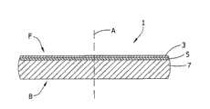
现在参考图1,在本发明的不同方面中,提供一种半导体晶片1,其具有改善的热导率。半导体晶片1具有前表面F、后表面B以及假想的中心轴A,在上下文中使用的术语“前”和“后”仅仅区分晶片的两个主要的、通常为平坦的表面。半导体晶片1还包括硅器件层3、硅保护层5和衬底7。Referring now to FIG. 1 , in a different aspect of the invention, a
为了抑制各种公知的器件失效机理,衬底7的热导率优选比保护层5的热导率至少大5%(在不超过125℃的温度下)。更优选地,衬底7的热导率比保护层5的热导率至少大10%(在不超过125℃的温度下)。例如,在某些实施例中,在不超过125℃的温度下,衬底7的热导率将比保护层5的热导率至少大15%、至少大20%或甚至至少大25%。To suppress various known device failure mechanisms, the thermal conductivity of the
现在参考图2,半导体晶片1具有假想的半径R,其从轴A延伸到半导体晶片1的边缘E。因为本发明的半导体晶片用作器件制造工艺的初始材料,所以通常优选器件层3和硅保护层5实质上延伸跨过晶片的直径。也就是说,通常优选器件层3和硅保护层5合并且关于轴A对称地设置,并且从该轴至半导体晶片边缘E延伸半径R的长度的至少90%。更优选地,器件层3和硅保护层5合并且关于轴A对称地设置,并且从该轴至半导体晶片边缘E延伸半径R的长度的至少99%。Referring now to FIG. 2 , the
现在参考图3,示例了本发明的示例性半导体晶片的载流子浓度分布。如所示出的,半导体晶片的器件层(晶片的从深度为0到约2μm的区域)具有约1.0×10¹⁶原子/cm3的掺杂剂浓度,硅保护层(晶片的深度为约3到约5μm的区域)具有1.0×1019原子/cm3的掺杂剂浓度,衬底(晶片的深度大于约6μm的区域)具有约1.0×1015原子/cm3的掺杂剂浓度。根据本发明,当选择半导体材料用于衬底时,可以将P型或N型掺杂剂用于掺杂器件层32、保护层33和衬底34中的每一个。Referring now to FIG. 3 , there is illustrated a carrier concentration profile for an exemplary semiconductor wafer of the present invention. As shown, the device layer of the semiconductor wafer (the region of the wafer from a depth of 0 to about 2 μm) has a dopant concentration of about 1.0×10¹⁶ atoms/cm3 , the silicon capping layer (the depth of the wafer is about 3 The region to about 5 μm) has a dopant concentration of 1.0×10¹⁹ atoms/cm3 , and the substrate (the region of the wafer deeper than about 6 μm) has a dopant concentration of about 1.0×10¹⁵ atoms/cm3 . According to the present invention, when a semiconductor material is selected for the substrate, either P-type or N-type dopants may be used to dope each of device layer 32 , protective layer 33 and substrate 34 .
I.衬底I. Substrate
通常,衬底包括一材料,该材料上可以形成另外的层,且该材料典型地具有至少约120W/m·K的热导率。衬底可以包括材料的单个层,或其可以包括多个层。然而,典型地,衬底是从根据例如Czochralski(“Cz”)或区熔法的已知技术中的一种生长的单晶硅锭切割来的。因此,为了示例的目的,这里利用单晶硅晶片作为参考。因此,在一个应用中,用于本发明晶片的初始材料是从根据Cz晶体生长方法生长的单晶锭切下的硅衬底,其典型地具有150mm、200mm、300mm或更大的标称直径。该衬底可以被抛光,或可替换地,被研磨和刻蚀而不被抛光。在例如Fumio Shimura,Semiconductor Silicon Crystal Technology(1989)和Silicon ChemicalEtching(Josef Grabmaier ed.,1982)中公开了这种方法以及标准的硅切割技术。优选地,通过本领域技术人员公知的标准方法抛光和清洁衬底。例如参见Handbook of Semiconductor Silicon Technology(William C.O’Mara et al.eds.,1990)。Typically, the substrate includes a material on which additional layers may be formed, and the material typically has a thermal conductivity of at least about 120 W/m·K. A substrate may comprise a single layer of material, or it may comprise multiple layers. Typically, however, the substrate is cut from a monocrystalline silicon ingot grown according to one of the known techniques such as Czochralski ("Cz") or zone melting. Therefore, for example purposes, a single crystal silicon wafer is utilized here as a reference. Thus, in one application, the starting material for the wafers of the present invention is a silicon substrate cut from a single crystal ingot grown according to the Cz crystal growth method, which typically has a nominal diameter of 150mm, 200mm, 300mm or more . The substrate can be polished, or alternatively, ground and etched without polishing. This method, as well as standard silicon dicing techniques, are disclosed, for example, in Fumio Shimura, Semiconductor Silicon Crystal Technology (1989) and Silicon Chemical Etching (Josef Grabmaier ed., 1982). Preferably, the substrate is polished and cleaned by standard methods known to those skilled in the art. See, for example, Handbook of Semiconductor Silicon Technology (William C.O'Mara et al.eds., 1990).
通常,单晶硅衬底被轻掺杂,以便其成为P-或N-硅,这些符号表示被常规地用于本领域中且描述于此。也就是说,对于P型掺杂应用,硅衬底通常具有小于约1×10¹⁶载流子/cm3,例如小于约5×1015载流子/cm3。而且,衬底典型地包含至少约5×1014载流子/cm3以最小化在较低掺杂水平下观察到的不期望的现象,例如有关氧的热施主产生。例如,P掺杂的单晶硅衬底典型地具有在约5×1014载流子/cm3和约1×1016载流子/cm3之间。对于N型掺杂应用,硅衬底通常具有小于约5×1015载流子/cm3,例如小于约1×1015载流子/cm3。Typically, a single crystal silicon substrate is lightly doped so that it becomes either P- or N-silicon, these notations are conventionally used in the art and are described herein. That is, for P-type doping applications, the silicon substrate typically has less than about 1×10¹⁶ carriers/cm3 , such as less than about 5×10¹⁵ carriers/cm3 . Also, the substrate typically contains at least about 5×10¹⁴ carriers/cm3 to minimize undesired phenomena observed at lower doping levels, such as oxygen-related thermal donor generation. For example, a P-doped single crystal silicon substrate typically has between about 5×10¹⁴ carriers/cm3 and about 1×10¹⁶ carriers/cm3 . For N-type doping applications, silicon substrates typically have less than about 5×10¹⁵ carriers/cm3 , such as less than about 1×10¹⁵ carriers/cm3 .
在另一方面中,硅衬底具有比P++或N++硅的热导率至少大出约5%的热导率,这些术语常规地用于本领域中且描述于此。通常,掺杂的硅的热导率与掺杂水平和大气温度相反地相关;即,掺杂的硅的热导率随着掺杂剂浓度和大气温度增加而降低。采集的数据表明,在室温下,P++或N++硅显示出小于约114W/m·K的热导率。因此,硅衬底的热导率大于约120W/m·K。更典型地,硅衬底的热导率大于约130W/m·K,例如大于约135W/m·K。在某些应用中,热导率将大于约140W/m·K,或甚至大于约150W/m·K。In another aspect, the silicon substrate has a thermal conductivity that is at least about 5% greater than that of P++ or N++ silicon, as these terms are conventionally used in the art and described herein. In general, the thermal conductivity of doped silicon is inversely related to doping level and atmospheric temperature; that is, the thermal conductivity of doped silicon decreases with increasing dopant concentration and atmospheric temperature. The collected data indicate that at room temperature, P++ or N++ silicon exhibits a thermal conductivity of less than about 114 W/m·K. Therefore, the thermal conductivity of the silicon substrate is greater than about 120 W/m·K. More typically, the thermal conductivity of the silicon substrate is greater than about 130 W/m·K, such as greater than about 135 W/m·K. In some applications, the thermal conductivity will be greater than about 140 W/m·K, or even greater than about 150 W/m·K.
单晶硅衬底包含至少一种掺杂剂,以使衬底具有各种所希望的性质。例如,衬底可以包括P型掺杂剂(即选自元素周期表的3族的元素,例如,硼、铝、镓和铟)或N型掺杂剂(即选自元素周期表的5族的元素,例如磷、砷、锑)。当希望P型掺杂时,掺杂剂优选为硼。当希望N型掺杂时,掺杂剂优选为磷。Single crystal silicon substrates contain at least one dopant to impart various desirable properties to the substrate. For example, the substrate may include a P-type dopant (i.e., an element selected from
II.保护层II. Protective layer
保护层典型地包括高掺杂的硅来提供保护,以免遭受常见的器件失效机理,例如闩锁和低扩散电流失效。根据应用,上文提及的合适的P型或N型掺杂剂中的任何一种都可以用于形成保护层。通常,保护层典型地包括大于约1×10¹⁸载流子/cm3。例如,对于P型掺杂应用,高掺杂的硅保护层包括在约1×1018载流子/cm3和约1×1020载流子/cm3之间。当掺杂剂浓度被表征为P++时,通常的范围包括在约8.5×1018载流子/cm3和约2.0×1019载流子/cm3之间,而当掺杂剂浓度被表征为P+时,通常的范围包括在约3.2×1018载流子/cm3和约8.5×1019载流子/cm3之间。在一个优选实施例中,保护层的掺杂剂浓度在约1.0×1019载流子/cm3和约1.25×1019载流子/cm3之间。对于N型掺杂应用,高掺杂的硅保护层包括在约6.0×1017载流子/cm3和约5×1019载流子/cm3之间。当掺杂剂浓度被表征为N++时,通常的范围包括在约1.2×1019载流子/cm3和约3.5×1019载流子/cm3之间,而当掺杂剂浓度被表征为N+时,通常的范围包括在约6.0×1017载流子/cm3和约4.5×1018载流子/cm3之间。The protective layer typically includes highly doped silicon to provide protection from common device failure mechanisms such as latch-up and low diffusion current failure. Depending on the application, any of the above-mentioned suitable P-type or N-type dopants may be used to form the protective layer. In general, the protective layer typically includes greater than about 1×10¹⁸ carriers/cm3 . For example, for P-type doping applications, the highly doped silicon capping layer includes between about 1×10¹⁸ carriers/cm3 and about 1×10²⁰ carriers/cm3 . Typical ranges are comprised between about 8.5×10¹⁸ carriers/cm3 and about 2.0×10¹⁹ carriers/cm3 when the dopant concentration is characterized as P++, and when the dopant concentration is characterized as For P+, the typical range includes between about 3.2×10¹⁸ carriers/cm3 and about 8.5×10¹⁹ carriers/cm3 . In a preferred embodiment, the protective layer has a dopant concentration between about 1.0×10¹⁹ carriers/cm3 and about 1.25×10¹⁹ carriers/cm3 . For N-type doping applications, the highly doped silicon capping layer comprises between about 6.0×10¹⁷ carriers/cm3 and about 5×10¹⁹ carriers/cm3 . Typical ranges are comprised between about 1.2×10¹⁹ carriers/cm3 and about 3.5×10¹⁹ carriers/cm3 when the dopant concentration is characterized as N++, and when the dopant concentration is characterized as For N+, typical ranges include between about 6.0×10¹⁷ carriers/cm3 and about 4.5×10¹⁸ carriers/cm3 .
另一方面,保护层的特征在于热导率低于衬底的热导率。也就是说,保护层的特征在于,在室温下,热导率小于约114W/m·K。例如,保护层的特征在于,在室温下,热导率小于约110W/m·K,或甚至小于约100W/m·K。On the other hand, the protective layer is characterized by a thermal conductivity lower than that of the substrate. That is, the protective layer is characterized by a thermal conductivity of less than about 114 W/m·K at room temperature. For example, the protective layer is characterized by a thermal conductivity of less than about 110 W/m·K, or even less than about 100 W/m·K at room temperature.
根据以上提及的衬底的热导率,衬底具有大于约120W/m·K的热导率且保护层具有小于约114W/m·K的热导率。例如,在一个应用中,衬底的热导率大于130W/m·K,且保护层的热导率小于约114W/m·K。在另一应用中,衬底的热导率大于135W/m·K,且保护层的热导率小于约110W/m·K。From the thermal conductivity of the substrate mentioned above, the substrate has a thermal conductivity of greater than about 120 W/m·K and the protective layer has a thermal conductivity of less than about 114 W/m·K. For example, in one application, the thermal conductivity of the substrate is greater than 130 W/m·K and the thermal conductivity of the protective layer is less than about 114 W/m·K. In another application, the thermal conductivity of the substrate is greater than 135 W/m·K and the thermal conductivity of the protective layer is less than about 110 W/m·K.
保护层的电阻率是另一种评估载流子浓度的方法。保护层的电阻率通常在约2.5mΩ·cm和约25mΩ·cm之间,其中通常的范围是在约5mΩ·cm和约10mΩ·cm之间以及在约10mΩ·cm和约20mΩ·cm之间。在一个优选实施例中,保护层的电阻率为约8mΩ·cm。The resistivity of the protective layer is another way to evaluate the carrier concentration. The resistivity of the protective layer is typically between about 2.5 mΩ·cm and about 25 mΩ·cm, with typical ranges being between about 5 mΩ·cm and about 10 mΩ·cm and between about 10 mΩ·cm and about 20 mΩ·cm. In a preferred embodiment, the protective layer has a resistivity of about 8 mΩ·cm.
通常,保护层足够厚以提供所希望的保护,但是应尽可能薄以促进热量从器件层传递到高热导率衬底。典型地,保护层为至少约1μm厚,例如在约1μm和约10μm之间。更典型地,保护层的厚度将在约1μm和约5μm之间;且对于某些应用,保护层的厚度将在约1μm和约3μm之间。Typically, the protective layer is thick enough to provide the desired protection, but as thin as possible to facilitate heat transfer from the device layer to the high thermal conductivity substrate. Typically, the protective layer is at least about 1 μm thick, such as between about 1 μm and about 10 μm. More typically, the thickness of the protective layer will be between about 1 μm and about 5 μm; and for some applications, the thickness of the protective layer will be between about 1 μm and about 3 μm.
用于在硅衬底上形成重掺杂硅保护层的任何公知技术都可以用于形成保护层。例如,保护层可以通过利用外延沉积、离子注入以及气相掺杂加高温扩散来形成。这些技术中的每一种都是公知的且进一步详细描述于本领域技术人员可以容易获得的参考文献中,例如Stanley Wolf & R.N.Tauber,Silicon Processing for the VLSI Era-Process Technology(1st ed.1986)和Stephen A.Campbell,The Science and Engineering ofMicroelectronic Fabrication(2nd ed.2001)。Any known technique for forming a heavily doped silicon protective layer on a silicon substrate can be used to form the protective layer. For example, the protective layer can be formed by utilizing epitaxial deposition, ion implantation, and gas phase doping plus high temperature diffusion. Each of these technologies is well known and described in further detail in references readily available to those skilled in the art, such as Stanley Wolf & R.N. Tauber, Silicon Processing for the VLSI Era-Process Technology (1st ed. 1986) and Stephen A. Campbell, The Science and Engineering of Microelectronic Fabrication (2nd ed. 2001).
外延层可以通过本领域通常已知的手段,例如描述于美国专利5789309中的外延生长工艺而沉积或生长在上述衬底的表面上。典型地,通过化学气相沉积实现外延层的生长,因为这是用于在半导体材料上生长外延层的最灵活和最具成本效率的方法之一。通过外延沉积形成保护层的一个优点在于,在外延生长期间,现有的外延生长反应器可以与直接掺杂剂供给联合使用。例如,当用硼掺杂硅时,高浓度的乙硼烷源气体可以与载气混合,用于掺杂外延生长的保护层。The epitaxial layer may be deposited or grown on the surface of the aforementioned substrate by means generally known in the art, such as the epitaxial growth process described in US Pat. No. 5,789,309. Typically, the growth of epitaxial layers is achieved by chemical vapor deposition, as this is one of the most flexible and cost-effective methods for growing epitaxial layers on semiconductor materials. One advantage of forming the protective layer by epitaxial deposition is that existing epitaxial growth reactors can be used in conjunction with direct dopant supply during epitaxial growth. For example, when doping silicon with boron, a high concentration of diborane source gas can be mixed with the carrier gas for doping the protective layer for epitaxial growth.
在另一实施例中,将离子注入技术用于迫使掺杂剂原子进入到单晶硅衬底中。在又一实施例中,将气相掺杂技术用于迫使掺杂剂原子进入到单晶硅衬底中。当使用离子注入或气相掺杂技术时,在升高的温度下执行该技术,或随后执行高温退火,以使掺杂剂原子扩散到衬底中而形成保护层。In another embodiment, ion implantation techniques are used to force dopant atoms into the single crystal silicon substrate. In yet another embodiment, vapor phase doping techniques are used to force dopant atoms into the single crystal silicon substrate. When ion implantation or vapor phase doping techniques are used, the techniques are performed at elevated temperatures, or followed by a high temperature anneal, to diffuse dopant atoms into the substrate to form a protective layer.
与用于形成高掺杂的硅保护层的特定技术无关地,由高掺杂的保护层到轻掺杂的衬底之间的过渡产生的掺杂剂分布还产生电场,该电场将过量的电荷载流子从该界面导入到衬底中。通过产生使电荷载流子从保护层移走并因此从器件层移走的电场,保护层还有效地降低辐射引起的效应或失效的影响。Regardless of the particular technique used to form the highly doped silicon cap layer, the dopant profile created by the transition between the highly doped cap layer to the lightly doped substrate also generates an electric field that displaces excess Charge carriers are introduced into the substrate from this interface. The protective layer also effectively reduces the effects of radiation-induced effects or failures by creating an electric field that dislodges charge carriers from the protective layer and thus from the device layer.
III.器件层III. Device layer
通常,器件层足够厚以包括至少一个级(level)的电器件。器件层可以包括多于一个级的电器件;因此,厚度可以根据特定应用所需的级数而变化。器件层的厚度通常小于约25μm。例如,器件层的厚度将典型地在约1μm和约25μm之间。对于某些应用,器件层的厚度将在约1μm和约20μm之间。在其它应用中,器件层的厚度将在约1μm和约10μm之间。在另外的其它应用中,例如在高速微处理器器件中,器件层的厚度将在约1μm和约5μm之间。可替换地,对于某些应用,例如功率器件,器件层的厚度将在约5μm和约20μm之间。Typically, the device layer is thick enough to include at least one level of electrical devices. A device layer may include more than one level of electrical device; thus, the thickness may vary depending on the number of levels required for a particular application. The thickness of the device layer is typically less than about 25 μm. For example, the thickness of the device layer will typically be between about 1 μm and about 25 μm. For some applications, the thickness of the device layer will be between about 1 μm and about 20 μm. In other applications, the thickness of the device layer will be between about 1 μm and about 10 μm. In still other applications, such as in high speed microprocessor devices, the thickness of the device layer will be between about 1 μm and about 5 μm. Alternatively, for certain applications, such as power devices, the thickness of the device layer will be between about 5 μm and about 20 μm.
为了产生器件层,半导体晶片可以经历如上所述的任何合适的外延沉积技术。执行生长的时间足以在外延生长反应器中形成希望厚度的器件层。器件层可以在生长外延层之后或与其生长的同时被掺杂。当在生长期间掺杂器件层时,可以采用直接掺杂剂供给;例如在用硼掺杂硅时,可以使用乙硼烷源气体。掺杂剂水平与常规硅器件层一致,以便其典型地称作P、P-、N或N-。即,器件层典型地包括在约7.5×10¹⁴载流子/cm3和约2.5×1016载流子/cm3之间。例如,器件层典型地包括在约1×1015载流子/cm3和约1×1016载流子/cm3之间。根据应用,可以使用上述合适的P型(例如硼)或N型掺杂剂(例如磷)中的任何一种。用P型掺杂剂掺杂的器件层的典型应用包括例如高速微处理器器件,例如存储器和逻辑应用。用N型掺杂剂掺杂的器件层的典型应用包括例如功率器件。To produce the device layers, the semiconductor wafer may be subjected to any suitable epitaxial deposition technique as described above. Growth is performed for a time sufficient to form the desired thickness of the device layer in the epitaxial growth reactor. The device layer can be doped after or simultaneously with the growth of the epitaxial layer. When doping the device layers during growth, a direct dopant supply can be used; for example, when doping silicon with boron, a diborane source gas can be used. The dopant levels are consistent with conventional silicon device layers so that they are typically referred to as P, P-, N or N-. That is, the device layer typically includes between about 7.5×10¹⁴ carriers/cm3 and about 2.5×10¹⁶ carriers/cm3 . For example, the device layer typically includes between about 1×10¹⁵ carriers/cm3 and about 1×10¹⁶ carriers/cm3 . Depending on the application, any of the suitable P-type (eg boron) or N-type dopants (eg phosphorous) described above may be used. Typical applications for device layers doped with P-type dopants include, for example, high speed microprocessor devices such as memory and logic applications. Typical applications of device layers doped with N-type dopants include, for example, power devices.
IV.所产生的晶片特性和应用IV. PRODUCTION WAFER CHARACTERISTICS AND APPLICATIONS
A.背面自动掺杂的防止A. Prevention of Backside Autodoping
在一个实施例中,利用本发明形成P/P+/P-半导体结构,即,本发明可以用于形成具有高掺杂的P+保护层以及中度掺杂的P器件层的轻掺杂P-衬底。这种半导体结构可以用在其中需要避免背面自动掺杂的应用中,例如其中不希望有氧化物密封的具有轻掺杂器件层的重掺杂衬底,正如具有双面抛光的结构的情况一样。通过根据本发明形成P/P+/P-半导体结构,实现了从器件层到保护层的P到P+过渡的功能等价,另一益处是避免了由于衬底的较低掺杂水平而使掺杂剂原子从结构的背面迁移到器件层。在该应用中,衬底具有约1×1016载流子/cm3以下的掺杂剂水平,P+保护层具有在约3.2×1018载流子/cm3和约8.5×1018载流子/cm3之间的掺杂剂水平,且器件层具有在约1×1014载流子/cm3和约4×1016载流子/cm3之间的掺杂剂水平。保护层还可以是P++层,其具有在约8.5×1018载流子/cm3和约2.0×1019载流子/cm3之间。而且,P+保护层的厚度典型地在约1μm和约10μm之间,而器件层的厚度典型地在约2μm和约5μm之间。In one embodiment, the present invention is used to form a P/P+/P- semiconductor structure, that is, the present invention can be used to form a lightly doped P- substrate. Such semiconductor structures can be used in applications where backside autodoping needs to be avoided, such as heavily doped substrates with lightly doped device layers where oxide encapsulation is undesirable, as is the case for structures with double-sided polishing . By forming a P/P+/P- semiconductor structure according to the present invention, the functional equivalence of the P to P+ transition from the device layer to the protective layer is achieved, another benefit is to avoid the doping due to the lower doping level of the substrate. The dopant atoms migrate from the backside of the structure to the device layer. In this application, the substrate has a dopant level below about 1×10¹⁶ carriers/cm3 and the P+ protective layer has about 3.2×10¹⁸ carriers/cm3 and about 8.5×10¹⁸ carriers /cm3 , and the device layer has a dopant level between about 1×10¹⁴ carriers/cm3 and about 4×10¹⁶ carriers/cm3 . The protective layer may also be a P++ layer having between about 8.5×10¹⁸ carriers/cm3 and about 2.0×10¹⁹ carriers/cm3 . Also, the thickness of the P+ protective layer is typically between about 1 μm and about 10 μm, while the thickness of the device layer is typically between about 2 μm and about 5 μm.
B.背面照明应用B. Backside lighting application
另外,根据本发明形成的P/P++/P-的半导体结构有利于制造用于背面照明应用例如改进的CMOS图像传感器器件中的薄硅结构。图16示出在该应用中用于典型的P/P++/P-半导体结构的典型载流子浓度分布。在形成P/P++/P-半导体结构之后,P-衬底的后表面暴露于碱性刻蚀剂一段时间,该时间段足以基本上去除所有衬底材料并获得具有高度均匀厚度的均匀减薄的P/P++硅结构。即,在本发明的该应用中,高掺杂P++(或甚至是P+++)保护层作为碱性刻蚀剂的刻蚀停止层。典型的刻蚀剂包括例如适当浓度的四甲基氢氧化铵(TMAH)、氢氧化钾(KOH)和氢氧化钠(NaOH)的化合物。在一个优选应用中,将TMAH用于碱性刻蚀剂中,其中TMAH的一个优选浓度是约25wt%。高掺杂的保护层作为使用碱性刻蚀剂的刻蚀停止层,这是因为P-衬底以比P++保护层的刻蚀速率快约10倍到约20倍的刻蚀速率被刻蚀。例如,图10图示了可以怎样将碱性刻蚀剂用于将材料学去除到至少在约10μm处所示的垂直虚线,以及可能地将材料去除到在约6μm处所示的垂直虚线。为该应用执行的刻蚀可以可选地发生在电化学电池中,其将增加刻蚀速率且在刻蚀之后促进可选择的电化学钝化步骤。In addition, P/P++/P- semiconductor structures formed according to the present invention facilitate the fabrication of thin silicon structures for backside illumination applications such as in improved CMOS image sensor devices. Figure 16 shows a typical carrier concentration profile for a typical P/P++/P- semiconductor structure in this application. After forming the P/P++/P- semiconductor structure, the rear surface of the P-substrate is exposed to an alkaline etchant for a period of time sufficient to remove substantially all of the substrate material and obtain a uniform thinning with a highly uniform thickness The P/P++ silicon structure. That is, in this application of the invention, the highly doped P++ (or even P+++) protective layer acts as an etch stop layer for the alkaline etchant. Typical etchants include compounds such as tetramethylammonium hydroxide (TMAH), potassium hydroxide (KOH), and sodium hydroxide (NaOH) in appropriate concentrations. In a preferred application, TMAH is used in the alkaline etchant, wherein a preferred concentration of TMAH is about 25 wt%. The highly doped protective layer acts as an etch stop using an alkaline etchant since the P- substrate is etched at about 10 to about 20 times faster etching rate than the P++ protective layer . For example, FIG. 10 illustrates how an alkaline etchant can be used to remove material to at least the dashed vertical line shown at about 10 μm, and possibly to the dashed vertical line shown at about 6 μm. Etching performed for this application may optionally take place in an electrochemical cell, which will increase the etch rate and facilitate an optional electrochemical passivation step after etching.
可选择地,在将P-衬底的剩余后表面暴露于碱性化学刻蚀剂之前,采用机械手段,例如研磨或抛光,来去除P-衬底的后表面的大部分(substantial portion)。在这种情况下,在采用碱性刻蚀剂之前,使用机械手段去除P-衬底厚度的大于约75%,例如去除衬底厚度的大于约80%、90%或甚至大于约95%。例如,再次参考图10,机械手段可以用于将材料去除到至少在约10μm处所示的垂直虚线,且接着碱性刻蚀剂可以用于将另外的材料去除到在约6μm处所示的垂直虚线。而且,可选择地,由衬底的去除所暴露的P++表面暴露于酸性刻蚀剂,以进一步减薄P/P++硅结构和进一步平滑化P++表面。在一个应用中,例如,酸性刻蚀剂包括氢氟酸、硝酸和乙酸的溶液(HNA)。再次参考图10,酸性刻蚀剂可以用于去除从在约6μm处所示的垂直虚线到在约3μm处所示的垂直虚线的材料。Optionally, a substantial portion of the rear surface of the P-substrate is removed using mechanical means, such as grinding or polishing, prior to exposing the remaining rear surface of the P-substrate to an alkaline chemical etchant. In this case, mechanical means are used to remove greater than about 75% of the thickness of the P-substrate, such as greater than about 80%, 90%, or even greater than about 95% of the thickness of the substrate, prior to employing the alkaline etchant. For example, referring again to FIG. 10, mechanical means can be used to remove material to at least the vertical dashed line shown at about 10 μm, and then an alkaline etchant can be used to remove additional material to the vertical dashed line shown at about 6 μm. Vertical dotted line. Also, optionally, the P++ surface exposed by the removal of the substrate is exposed to an acidic etchant to further thin the P/P++ silicon structure and further smooth the P++ surface. In one application, for example, the acidic etchant includes a solution of hydrofluoric acid, nitric acid, and acetic acid (HNA). Referring again to FIG. 10, an acidic etchant may be used to remove material from the vertical dashed line shown at about 6 μm to the vertical dashed line shown at about 3 μm.
在该应用中,衬底具有约1×10¹⁶载流子/cm3以下的掺杂剂水平,保护层具有大于约1×1019载流子/cm3,例如在约1×1019载流子/cm3和约1.0×1020载流子/cm3之间的掺杂剂水平。例如,保护层可以具有在约5.0×1019载流子/cm3和约1.0×1020载流子/cm3之间。以这样的浓度掺杂的硅通常称作高掺杂P++或甚至P+++硅层。而且,在该应用中限制保护层的厚度,其中较高的掺杂浓度对应于较薄的保护层。例如,作为刻蚀停止层的保护层的典型厚度小于约5μm,例如小于2μm,小于约1μm或甚至小于约0.5μm。在一个应用中,保护层进一步包括Ge,以作为晶格应变缓和物(reliever),该晶格应变缓和物允许高掺杂的保护层具有比以上报导的更大的厚度。最后,器件层的厚度典型地在约2μm和约15μm之间,例如厚度在约2μm和约10μm之间。在一个应用中,器件层是在约2μm和约5μm之间。In this application, the substrate has a dopant level below about 1×10¹⁶ carriers/cm3 and the protective layer has more than about 1×10¹⁹ carriers/cm3 , for example at about 1×10¹⁹ carriers/cm3 and about 1.0×10²⁰ carriers/cm3 for dopant levels. For example, the protective layer may have between about 5.0×10¹⁹ carriers/cm3 and about 1.0×10²⁰ carriers/cm3 . Silicon doped at such concentrations is often referred to as a highly doped P++ or even P+++ silicon layer. Furthermore, the thickness of the protective layer is limited in this application, wherein higher doping concentrations correspond to thinner protective layers. For example, a typical thickness of a protective layer as an etch stop layer is less than about 5 μm, such as less than 2 μm, less than about 1 μm or even less than about 0.5 μm. In one application, the protective layer further comprises Ge as a lattice strain reliever that allows a highly doped protective layer with a greater thickness than reported above. Finally, the thickness of the device layer is typically between about 2 μm and about 15 μm, for example between about 2 μm and about 10 μm thick. In one application, the device layer is between about 2 μm and about 5 μm.
所得到的P/P++硅结构的背面P++表面是平滑的,这最小化了背面照明期间的光散射。而且,由从器件层到保护层的过渡而形成的掺杂梯度产生电场,该电场促进电子从背面照明的表面迁移出来且朝向器件层迁移,这在图像传感器器件中是有利的,因为在光电二极管结处量子效率增大。The backside P++ surface of the resulting P/P++ silicon structure is smooth, which minimizes light scattering during backside illumination. Moreover, the doping gradient formed by the transition from the device layer to the protective layer generates an electric field that facilitates the migration of electrons from the back-illuminated surface and towards the device layer, which is advantageous in image sensor devices because in optoelectronic The quantum efficiency increases at the diode junction.
已经详细描述了本发明,在不脱离所附的权利要求限定的本发明的范围的情况下,显然可以进行修改和变化。Having described the invention in detail, it will be apparent that modifications and changes may be made without departing from the scope of the invention as defined in the appended claims.
实例example
提供下列非限制性实例以进一步示例本发明。The following non-limiting examples are provided to further illustrate the invention.
实例1Example 1
准备两种类型的半导体晶片,第一种类型具有P-衬底,代表本发明的示例性半导体晶片,以及第二种类型具有P++衬底,代表本领域已知的半导体晶片。P型掺杂剂用于每一种类型的半导体晶片。具有P-衬底的半导体晶片具有这样的载流子浓度分布,其中浓度为约1×10¹⁶载流子/cm3的器件层延伸到晶片中约2μm,浓度为约1×1019载流子/cm3的保护层延伸到晶片中是约3到约5μm的深度,以及浓度为约1×1015载流子/cm3的衬底从约6μm延伸穿过晶片的深度。具有P++衬底的半导体晶片具有这样的载流子浓度分布,其中浓度为约1×1016载流子/cm3的器件层延伸到晶片中约2μm,以及浓度为约1×1019载流子/cm3的衬底从约3μm延伸穿过晶片的深度。每种类型的半导体晶片的掺杂分布分别在图3和4中示出。Two types of semiconductor wafers were prepared, the first type having a P-substrate, representing an exemplary semiconductor wafer of the present invention, and the second type having a P++ substrate, representing a semiconductor wafer known in the art. P-type dopants are used in every type of semiconductor wafer. A semiconductor wafer with a P-substrate has a carrier concentration profile in which a device layer with a concentration of about 1×10¹⁶ carriers/cm3 extends about 2 μm into the wafer with a concentration of about 1×10¹⁹ carriers The protective layer extends into the wafer to a depth of about 3 to about 5 μm in electrons/cm3 , and the substrate at a concentration of about 1×10¹⁵ carriers/cm3 extends from about 6 μm deep into the wafer. A semiconductor wafer with a P++ substrate has a carrier concentration profile in which a device layer with a concentration of about 1×10 carriers/cm extends about 2 μm into thewafer , and a concentration of about 1×10 carriers/cm sub/cm3 of substrate extending from about 3 μm to a depth across the wafer. The doping profiles for each type of semiconductor wafer are shown in Figures 3 and 4, respectively.
值得注意地,图3和4显示,与每种类型的半导体晶片相关联的载流子掺杂剂分布都是约4μm的相同深度,即,两种类型的晶片都在从晶片的前表面约2到3μm处有P/P++过渡。这种过渡证明器件失效保护存在于本发明的示例性半导体晶片的器件/保护层界面处。而且,在重掺杂的保护层和轻掺杂的衬底之间的界面处的掺杂梯度产生电场,该电场进一步减小了在器件层之下的衬底中产生的电荷载流子的聚集,从而改善了本发明的示例性半导体晶片中的保护层的保护功能。Notably, Figures 3 and 4 show that the carrier dopant profiles associated with each type of semiconductor wafer are at the same depth of about 4 μm, i.e., both types of wafers are at about 4 μm from the front surface of the wafer. There is a P/P++ transition at 2 to 3 μm. This transition demonstrates that device failure protection exists at the device/protective layer interface of the exemplary semiconductor wafer of the present invention. Moreover, the doping gradient at the interface between the heavily doped protective layer and the lightly doped substrate generates an electric field that further reduces the density of charge carriers generated in the substrate below the device layer. aggregation, thereby improving the protective function of the protective layer in the exemplary semiconductor wafer of the present invention.
然后,在均匀加热和局部热斑的两种条件下,对在图3和4中所示的晶片执行热建模(thermal modeling)。使用在轻掺杂P-和重掺杂P++衬底之间的公认的(accepted)20%热导率差异产生模拟。利用分布到代表理论上的芯片的20mm×20mm栅格的功率来建模两种条件,该理论上的芯片被分成1mm×1mm的栅格方块。为了在均匀加热条件下建模晶片,160W的工作功率被均匀地分散在20mm×20mm的栅格上。为了利用局部热斑建模晶片,增大为10倍的局部功率(即1600W)集中在两个分离的1mm×1mm的栅格方块中以模拟热斑,同时保持相同的总芯片工作功率。在两种条件下对250μm和500μm的芯片厚度执行建模。热建模的结果在下面示于表格1和2中,分别对应于均匀加热条件和局部热斑条件。建模还假定在衬底的底部处的热传递系数是0.84kW/m2K,该值是基于文献中所公开的数值。Thermal modeling was then performed on the wafers shown in Figures 3 and 4 under both conditions of uniform heating and localized hot spots. Simulations were generated using the accepted 20% thermal conductivity difference between lightly doped P- and heavily doped P++ substrates. Both conditions were modeled using power distributed to a 20 mm x 20 mm grid representing a theoretical chip divided into 1 mm x 1 mm grid squares. In order to model the wafer under uniform heating conditions, the operating power of 160 W was evenly distributed on a grid of 20 mm × 20 mm. To model the wafer with localized hot spots, a 10-fold increase in local power (ie, 1600W) was concentrated in two separate 1 mm x 1 mm grid squares to simulate hot spots while maintaining the same total chip operating power. Modeling was performed for chip thicknesses of 250 μm and 500 μm under two conditions. The results of the thermal modeling are shown below in Tables 1 and 2, corresponding to the uniform heating condition and the localized hot spot condition, respectively. The modeling also assumes a heat transfer coefficient of 0.84 kW/m2 K at the bottom of the substrate, a value based on values published in the literature.
表1Table 1

表2Table 2

热建模的结果显示,在均匀功率分布的情况下,两个晶片提供相似的热耗散。具体地,表1显示,与对应的P++衬底样品相比,两个P-衬底样品达到的最大芯片温度为,对于250μm样品仅低0.2℃以及对于500μm样品仅低0.3℃。这种热耗散的小的提升表明在均匀加热条件下,给定晶片的衬底的掺杂浓度对热耗散具有很小的影响。The results of thermal modeling show that, with uniform power distribution, both dies provide similar heat dissipation. In particular, Table 1 shows that the maximum chip temperature achieved for the two P-substrate samples is only 0.2°C lower for the 250μm sample and only 0.3°C lower for the 500μm sample compared to the corresponding P++ substrate sample. This small increase in heat dissipation indicates that under uniform heating conditions, the doping concentration of the substrate of a given wafer has little effect on heat dissipation.
但是在局部热斑的模型中,表2显示,具有P-衬底的半导体晶片从局部热斑更有效地散热。具体地,P-衬底晶片样品的结果是,与对应的P++衬底晶片的最大芯片温度相比,对于250μm样品,最大芯片温度低约5℃,而对于500μm样品,最大芯片温度低约4.4℃。But in the model of localized hot spots, Table 2 shows that semiconductor wafers with P-substrates dissipate heat more efficiently from localized hot spots. Specifically, the results for the P-substrate wafer sample are that the maximum die temperature is about 5°C lower for the 250 μm sample and about 4.4°C lower for the 500 μm sample compared to the maximum die temperature for the corresponding P++ substrate wafer. ℃.
还生成了等温线图,以由热斑模拟进一步示例晶片之间的差异。图5和6涉及具有约250μm总厚度的晶片,其中图5示出具有P++衬底的晶片的等温线图,以及图6示出具有P-衬底的晶片的等温线图。相似地,图7和8涉及具有约500μm总厚度的晶片,其中图7示出具有P++衬底的晶片的等温线图,以及图8示出具有P-衬底的晶片的等温线图。所有这四幅等温线图显示,在具有P-衬底的晶片中,1mm×1mm栅格方块热斑的温度没有在具有P++衬底的晶片中的那么强烈。Isotherm maps were also generated to further illustrate wafer-to-wafer differences from hot spot simulations. 5 and 6 relate to wafers having a total thickness of about 250 μm, wherein FIG. 5 shows an isotherm diagram for a wafer with a P++ substrate, and FIG. 6 shows an isotherm diagram for a wafer with a P− substrate. Similarly, FIGS. 7 and 8 relate to wafers having a total thickness of about 500 μm, wherein FIG. 7 shows an isotherm diagram for a wafer with a P++ substrate, and FIG. 8 shows an isotherm diagram for a wafer with a P− substrate. All four of these isotherm plots show that the temperature of the 1 mm x 1 mm grid square hot spot is not as intense in the wafer with P-substrate as in the wafer with P++ substrate.
实例2Example 2
除了在实例1中形成的两个半导体晶片,如下所述,形成七个另外的具有不同衬底的半导体晶片。除了下述样品95以外,所有的样品都是根据CZ生长方法形成的。In addition to the two semiconductor wafers formed in Example 1, seven additional semiconductor wafers having different substrates were formed as described below. All samples were formed according to the CZ growth method, except for
为了该实例的目的,将从实例1形成的具有P-衬底的半导体晶片称作样品91,而将具有P++衬底的半导体晶片称作样品92。For the purposes of this example, the semiconductor wafer formed from Example 1 with a P− substrate will be referred to as
此外,样品93是这样的半导体晶片,其实质上由P+材料,即,以本发明的保护层和衬底之间的水平例如约5×10¹⁸载流子/cm3掺杂的材料构成。Furthermore,
样品94是这样的半导体晶片,其实质上由同时掺杂有P-和N-掺杂水平的硅材料,即,包括小于约1×10¹⁶P型载流子/cm3和小于约1×1016N型载流子/cm3,例如每种掺杂剂约1×1015载流子/cm3的材料构成。
样品95是这样的半导体晶片,其实质上由根据区熔法形成且掺杂成如对于样品94所定义的P-材料的硅材料构成。
样品96是这样的半导体晶片,其实质上由掺杂成如对于样品94所定义的P-材料且具有低浓度的氧填隙子的硅材料构成。
样品97是这样的半导体晶片,其实质上由掺杂成如对于样品94所定义的P-材料且具有高浓度的氧填隙子的硅材料构成。
样品98是这样的半导体晶片结构,其具有掺杂成如对于样品94所定义的P-的P-材料的衬底和形成于衬底上的P-材料的外延层。P-外延层约10μm厚。
样品99是这样的半导体晶片结构,其具有掺杂成如对于样品94所定义的P-的P-材料的衬底和形成于衬底上的P-材料的外延层。P-外延层约50μm厚。
在25℃、50℃、75℃、100℃和125℃下,对样品91-99进行热导率测量。结果图示在图15中,其示出,与温度无关地,样品92的热导率最低,且样品91和94-99的热导率最高。样品91和94-99都显示出基本上相似的热导率分布的事实表明,这些样品之间变化的变量对它们的热导率影响很小。此外,样品93显示出介于样品92与样品组91和94-99之间的热导率。这证明硅结构的掺杂浓度是对热导率的影响最大的变量。而且,这些数据显示,在约25℃下,热导率从样品92到样品91和94-99增加了约23%,而在约125℃下,热导率从样品92到样品91和94-99增加了约13%。这证明,如在此所述的本发明的半导体结构显示出在约25℃和约125℃之间的温度下,热导率增加了至少5%。Thermal conductivity measurements were performed on samples 91-99 at 25°C, 50°C, 75°C, 100°C, and 125°C. The results are plotted in Figure 15, which shows that, independent of temperature,
当在此使用涉及掺杂剂的术语“掺杂剂”、“轻掺杂”、“重掺杂”或其它术语和短语时,应理解,除非另外明确说明,其是指P型或N型掺杂剂。When the terms "dopant," "lightly doped," "heavily doped," or other terms and phrases referring to dopants are used herein, it is to be understood that unless expressly stated otherwise, it refers to a P-type or N-type dopant.
当介绍本发明的要素或本发明的优选实施例时,冠词“一”、“该”和“所述,,意指表示存在一个或多个要素。术语“包括”、“包含”和“具有”旨在非遍举的,且表示可以存在除了所列的要素之外的其它要素。When introducing elements of the present invention or preferred embodiments of the present invention, the articles "a", "the" and "said" mean that there are one or more elements. The terms "comprising", "comprising" and " Having" is intended to be non-exclusive and means that there may be other elements than the listed elements.
综上所述,可以看出,实现了本发明的几个目标且获得了其它有利的结果。From the foregoing, it can be seen that the several objects of the invention are achieved and other advantageous results obtained.
由于在不脱离本发明的范围的情况下,可以对上述产品和方法作出各种改变,以上描述中所包含的和附图中所示出的所有内容都旨在解释为示例性的而非限制性的。As various changes could be made in the above products and methods without departing from the scope of the invention, it is intended that all matter contained in the above description and shown in the accompanying drawings shall be interpreted as illustrative and not in a limiting sense. sexual.
Claims (26)
Translated fromChineseApplications Claiming Priority (2)
| Application Number | Priority Date | Filing Date | Title |
|---|---|---|---|
| US76364306P | 2006-01-31 | 2006-01-31 | |
| US60/763,643 | 2006-01-31 |
Publications (1)
| Publication Number | Publication Date |
|---|---|
| CN101410977Atrue CN101410977A (en) | 2009-04-15 |
Family
ID=38121741
Family Applications (1)
| Application Number | Title | Priority Date | Filing Date |
|---|---|---|---|
| CNA200780011360XAPendingCN101410977A (en) | 2006-01-31 | 2007-01-26 | Semiconductor wafer with high thermal conductivity |
Country Status (8)
| Country | Link |
|---|---|
| US (3) | US20070176238A1 (en) |
| EP (3) | EP2637208A1 (en) |
| JP (1) | JP5261194B2 (en) |
| KR (2) | KR20080098632A (en) |
| CN (1) | CN101410977A (en) |
| MY (1) | MY153160A (en) |
| TW (1) | TWI429793B (en) |
| WO (1) | WO2007090055A1 (en) |
Families Citing this family (11)
| Publication number | Priority date | Publication date | Assignee | Title |
|---|---|---|---|---|
| US20090050939A1 (en)* | 2007-07-17 | 2009-02-26 | Briere Michael A | Iii-nitride device |
| KR20100077363A (en)* | 2008-12-29 | 2010-07-08 | 주식회사 동부하이텍 | Method for fabricating of cmos image sensor |
| US7985658B2 (en)* | 2009-06-08 | 2011-07-26 | Aptina Imaging Corporation | Method of forming substrate for use in imager devices |
| EP2555244A1 (en)* | 2011-08-03 | 2013-02-06 | austriamicrosystems AG | A method of producing a photodiode device and a photodiode device comprising an etch stop layer |
| US8748315B2 (en)* | 2012-02-15 | 2014-06-10 | Taiwan Semiconductor Manufacturing Co., Ltd. | Condition before TMAH improved device performance |
| US8956938B2 (en)* | 2012-05-16 | 2015-02-17 | International Business Machines Corporation | Epitaxial semiconductor resistor with semiconductor structures on same substrate |
| US9111898B2 (en)* | 2013-02-19 | 2015-08-18 | Taiwan Semiconductor Manufacturing Company. Ltd. | Multiple layer substrate |
| CN104064688B (en)* | 2014-07-11 | 2016-09-21 | 深圳市华星光电技术有限公司 | There is manufacture method and this TFT substrate of the TFT substrate of storage electric capacity |
| CN112776003B (en)* | 2019-11-07 | 2022-05-06 | 台达电子工业股份有限公司 | Heat sink and its applicable robot |
| CN112397570A (en)* | 2020-11-17 | 2021-02-23 | 华虹半导体(无锡)有限公司 | Semiconductor substrate structure and manufacturing method thereof |
| EP4576168A1 (en)* | 2023-12-22 | 2025-06-25 | Nexperia B.V. | Suppression of auto-doping during epitaxial growth of epitaxy layer in a semiconductor device |
Citations (1)
| Publication number | Priority date | Publication date | Assignee | Title |
|---|---|---|---|---|
| US4506436A (en)* | 1981-12-21 | 1985-03-26 | International Business Machines Corporation | Method for increasing the radiation resistance of charge storage semiconductor devices |
Family Cites Families (18)
| Publication number | Priority date | Publication date | Assignee | Title |
|---|---|---|---|---|
| US4104090A (en)* | 1977-02-24 | 1978-08-01 | International Business Machines Corporation | Total dielectric isolation utilizing a combination of reactive ion etching, anodic etching, and thermal oxidation |
| US4247862B1 (en)* | 1977-08-26 | 1995-12-26 | Intel Corp | Ionzation resistant mos structure |
| US4628591A (en)* | 1984-10-31 | 1986-12-16 | Texas Instruments Incorporated | Method for obtaining full oxide isolation of epitaxial islands in silicon utilizing selective oxidation of porous silicon |
| JPH0793282B2 (en)* | 1985-04-15 | 1995-10-09 | 株式会社日立製作所 | Method for manufacturing semiconductor device |
| FR2638892B1 (en)* | 1988-11-09 | 1992-12-24 | Sgs Thomson Microelectronics | METHOD FOR MODULATING THE QUANTITY OF GOLD DIFFUSED IN A SILICON SUBSTRATE AND RAPID DIODE OBTAINED BY THIS PROCESS |
| US5023200A (en)* | 1988-11-22 | 1991-06-11 | The United States Of America As Represented By The United States Department Of Energy | Formation of multiple levels of porous silicon for buried insulators and conductors in silicon device technologies |
| US5024723A (en)* | 1990-05-07 | 1991-06-18 | Goesele Ulrich M | Method of producing a thin silicon on insulator layer by wafer bonding and chemical thinning |
| JPH07187892A (en)* | 1991-06-28 | 1995-07-25 | Internatl Business Mach Corp <Ibm> | Silicon and its formation |
| JPH06151303A (en)* | 1992-11-11 | 1994-05-31 | Hitachi Ltd | Method for forming semiconductor wafer |
| US5880010A (en)* | 1994-07-12 | 1999-03-09 | Sun Microsystems, Inc. | Ultrathin electronics |
| US5668045A (en)* | 1994-11-30 | 1997-09-16 | Sibond, L.L.C. | Process for stripping outer edge of BESOI wafers |
| US5789309A (en)* | 1996-12-30 | 1998-08-04 | Memc Electronic Materials, Inc. | Method and system for monocrystalline epitaxial deposition |
| JPH10242153A (en)* | 1997-02-26 | 1998-09-11 | Hitachi Ltd | Semiconductor wafer, method of manufacturing semiconductor wafer, semiconductor device, and method of manufacturing semiconductor device |
| WO1998042010A1 (en) | 1997-03-17 | 1998-09-24 | Genus, Inc. | Bonded soi wafers using high energy implant |
| EP1148544A1 (en) | 2000-04-19 | 2001-10-24 | Infineon Technologies AG | Method for thinning a substrate |
| JP3785067B2 (en)* | 2001-08-22 | 2006-06-14 | 株式会社東芝 | Manufacturing method of semiconductor device |
| JP4211696B2 (en)* | 2004-06-30 | 2009-01-21 | ソニー株式会社 | Method for manufacturing solid-state imaging device |
| DE102004039197B4 (en)* | 2004-08-12 | 2010-06-17 | Siltronic Ag | Process for producing doped silicon wafers |
- 2007
- 2007-01-26KRKR1020087021333Apatent/KR20080098632A/ennot_activeCeased
- 2007-01-26EPEP13166827.9Apatent/EP2637208A1/ennot_activeWithdrawn
- 2007-01-26CNCNA200780011360XApatent/CN101410977A/enactivePending
- 2007-01-26WOPCT/US2007/061128patent/WO2007090055A1/enactiveApplication Filing
- 2007-01-26MYMYPI20082825Apatent/MY153160A/enunknown
- 2007-01-26JPJP2008553453Apatent/JP5261194B2/enactiveActive
- 2007-01-26EPEP13166824.6Apatent/EP2637207A1/ennot_activeWithdrawn
- 2007-01-26KRKR1020127021211Apatent/KR20120106893A/ennot_activeCeased
- 2007-01-26USUS11/698,728patent/US20070176238A1/ennot_activeAbandoned
- 2007-01-26EPEP07762756Apatent/EP1994562A1/ennot_activeWithdrawn
- 2007-01-31TWTW096103543Apatent/TWI429793B/enactive
- 2009
- 2009-05-19USUS12/454,512patent/US8080482B2/enactiveActive
- 2011
- 2011-09-02USUS13/199,587patent/US8865601B2/enactiveActive
Patent Citations (1)
| Publication number | Priority date | Publication date | Assignee | Title |
|---|---|---|---|---|
| US4506436A (en)* | 1981-12-21 | 1985-03-26 | International Business Machines Corporation | Method for increasing the radiation resistance of charge storage semiconductor devices |
Also Published As
| Publication number | Publication date |
|---|---|
| MY153160A (en) | 2015-01-29 |
| KR20080098632A (en) | 2008-11-11 |
| TWI429793B (en) | 2014-03-11 |
| JP2009525622A (en) | 2009-07-09 |
| WO2007090055A1 (en) | 2007-08-09 |
| EP2637207A1 (en) | 2013-09-11 |
| TW200801261A (en) | 2008-01-01 |
| US8865601B2 (en) | 2014-10-21 |
| US20110318912A1 (en) | 2011-12-29 |
| US20070176238A1 (en) | 2007-08-02 |
| EP2637208A1 (en) | 2013-09-11 |
| US8080482B2 (en) | 2011-12-20 |
| JP5261194B2 (en) | 2013-08-14 |
| EP1994562A1 (en) | 2008-11-26 |
| KR20120106893A (en) | 2012-09-26 |
| US20090233428A1 (en) | 2009-09-17 |
Similar Documents
| Publication | Publication Date | Title |
|---|---|---|
| CN101410977A (en) | Semiconductor wafer with high thermal conductivity | |
| CN106057934B (en) | Back contact solar cell device | |
| TWI520230B (en) | Image sensing device and method of manufacturing same | |
| TW201030953A (en) | Improving dark currents and reducing defects in image sensors and photovoltaic junctions | |
| TW201340351A (en) | Solar cell with an emitter region of a wide band gap semiconductor material | |
| KR20170132224A (en) | Polycrystalline Silicon for Blisterless Solar Cells | |
| KR20150112735A (en) | Cmos image sensor with epitaxial passivation layer | |
| EP2256820A2 (en) | Photo-electronic device comprising a vertical p-n or p-i-n junction and manufacturing method thereof | |
| US20160284917A1 (en) | Passivation Layer for Solar Cells | |
| CN103811572A (en) | Photoelectric device and method of manufacturing same | |
| CN103050545A (en) | TVS (Transient Voltage Suppressor) diode and manufacturing method thereof | |
| TWI401810B (en) | Solar battery | |
| US20140264500A1 (en) | Photovoltaic Device Formed On Porous Silicon Isolation | |
| TWI675490B (en) | Method of fabricating solar cells | |
| Steckenreiter et al. | Reuse of substrate wafers for the porous silicon layer transfer | |
| CN103515461A (en) | Textured multi-junction solar cell and fabrication method | |
| US20230197868A1 (en) | Integrated optical sensor of the single-photon avalanche photodiode type, and manufacturing method | |
| CN102386121A (en) | Manufacturing method of semiconductor device and semiconductor buried layer | |
| TWI686958B (en) | Solar cell and method of fabricating the same | |
| KR20110059366A (en) | Single crystal semiconductor substrate with separation region, solar cell using same and manufacturing method thereof | |
| WO2014086014A1 (en) | Itc-igbt and manufacturing method therefor | |
| CN104183668A (en) | Manufacturing method of solar cell unit | |
| CN119815929A (en) | Electrostatic discharge protection device with low capacitance | |
| Kim et al. | Study of the ion-implanted back-surface fields in front-contact front-junction solar cells | |
| TW202226332A (en) | Manufacturing method for SOI wafer, and SOI wafer |
Legal Events
| Date | Code | Title | Description |
|---|---|---|---|
| C06 | Publication | ||
| PB01 | Publication | ||
| C10 | Entry into substantive examination | ||
| SE01 | Entry into force of request for substantive examination | ||
| C12 | Rejection of a patent application after its publication | ||
| RJ01 | Rejection of invention patent application after publication | Application publication date:20090415 |