CN101395728B - Light emitting element and manufacturing method thereof - Google Patents
Light emitting element and manufacturing method thereofDownload PDFInfo
- Publication number
- CN101395728B CN101395728BCN2007800080907ACN200780008090ACN101395728BCN 101395728 BCN101395728 BCN 101395728BCN 2007800080907 ACN2007800080907 ACN 2007800080907ACN 200780008090 ACN200780008090 ACN 200780008090ACN 101395728 BCN101395728 BCN 101395728B
- Authority
- CN
- China
- Prior art keywords
- light
- layer
- semiconductor layer
- dbr
- emitting element
- Prior art date
- Legal status (The legal status is an assumption and is not a legal conclusion. Google has not performed a legal analysis and makes no representation as to the accuracy of the status listed.)
- Expired - Fee Related
Links
Images


Classifications
- H—ELECTRICITY
- H10—SEMICONDUCTOR DEVICES; ELECTRIC SOLID-STATE DEVICES NOT OTHERWISE PROVIDED FOR
- H10H—INORGANIC LIGHT-EMITTING SEMICONDUCTOR DEVICES HAVING POTENTIAL BARRIERS
- H10H20/00—Individual inorganic light-emitting semiconductor devices having potential barriers, e.g. light-emitting diodes [LED]
- H10H20/80—Constructional details
- H10H20/83—Electrodes
- H10H20/832—Electrodes characterised by their material
- H10H20/835—Reflective materials
- H—ELECTRICITY
- H10—SEMICONDUCTOR DEVICES; ELECTRIC SOLID-STATE DEVICES NOT OTHERWISE PROVIDED FOR
- H10H—INORGANIC LIGHT-EMITTING SEMICONDUCTOR DEVICES HAVING POTENTIAL BARRIERS
- H10H20/00—Individual inorganic light-emitting semiconductor devices having potential barriers, e.g. light-emitting diodes [LED]
- H10H20/80—Constructional details
- H10H20/81—Bodies
- H10H20/819—Bodies characterised by their shape, e.g. curved or truncated substrates
- H10H20/82—Roughened surfaces, e.g. at the interface between epitaxial layers
- H—ELECTRICITY
- H10—SEMICONDUCTOR DEVICES; ELECTRIC SOLID-STATE DEVICES NOT OTHERWISE PROVIDED FOR
- H10H—INORGANIC LIGHT-EMITTING SEMICONDUCTOR DEVICES HAVING POTENTIAL BARRIERS
- H10H20/00—Individual inorganic light-emitting semiconductor devices having potential barriers, e.g. light-emitting diodes [LED]
- H10H20/80—Constructional details
- H10H20/872—Periodic patterns for optical field-shaping, e.g. photonic bandgap structures
- H—ELECTRICITY
- H10—SEMICONDUCTOR DEVICES; ELECTRIC SOLID-STATE DEVICES NOT OTHERWISE PROVIDED FOR
- H10K—ORGANIC ELECTRIC SOLID-STATE DEVICES
- H10K50/00—Organic light-emitting devices
- H10K50/80—Constructional details
- H10K50/85—Arrangements for extracting light from the devices
- H10K50/854—Arrangements for extracting light from the devices comprising scattering means
- H—ELECTRICITY
- H10—SEMICONDUCTOR DEVICES; ELECTRIC SOLID-STATE DEVICES NOT OTHERWISE PROVIDED FOR
- H10K—ORGANIC ELECTRIC SOLID-STATE DEVICES
- H10K50/00—Organic light-emitting devices
- H10K50/80—Constructional details
- H10K50/85—Arrangements for extracting light from the devices
- H10K50/858—Arrangements for extracting light from the devices comprising refractive means, e.g. lenses
Landscapes
- Led Devices (AREA)
Abstract
Description
Translated fromChinese技术领域technical field
本发明涉及一种包括半导体的发光元件及其制造方法。The present invention relates to a light emitting element including a semiconductor and a manufacturing method thereof.
背景技术Background technique
近年来,利用III-V化合物(以下称为氮化物(nitride))或II-VI化合物,在其中形成量子阱(quantum well),并从外部流入电流,在该量子阱中使电子与空穴结合来产生光的发光元件有了显著发展。In recent years, using III-V compound (hereinafter referred to as nitride (nitride)) or II-VI compound, a quantum well (quantum well) is formed therein, and current flows in from the outside, and electrons and holes are separated in the quantum well. Light emitting elements combined to generate light have been significantly developed.
作为III-V化合物最常用的物质是所述氮化物的GaN。以该GaN为首的氮化物的折射率大于1,因此在从发光元件内向大气中取出光方面存在问题。以GaN的情况为例,由于折射率大约是2.5,因此相对于GaN与大气交界处的法线,以大于指定角度(例如23.6度)的角度射入交界处的光不被放射到大气中,而在交界面被全反射,被封闭于发光元件的GaN层中。以下,将在相对于所述法线小于指定角度的角度区域中形成的圆锥区域称为逃逸圆锥(escape cone)。The most commonly used substance as a III-V compound is GaN as the nitride. Since the refractive index of nitrides including GaN is greater than 1, there is a problem in extracting light from the inside of the light-emitting element to the atmosphere. In the case of GaN as an example, since the refractive index is about 2.5, light entering the junction at an angle greater than a specified angle (for example, 23.6 degrees) with respect to the normal of the junction between GaN and the atmosphere is not emitted into the atmosphere, However, it is totally reflected at the interface and is enclosed in the GaN layer of the light-emitting element. Hereinafter, a cone region formed in an angle region smaller than a specified angle with respect to the normal is referred to as an escape cone.
而且,被封闭于所述GaN层中的光的大部分重新被晶体、电极材料吸收并转化为热,而不能取出到外部。因此,存在在平坦的GaN层中,不能提高光取出效率的问题。Furthermore, most of the light confined in the GaN layer is absorbed again by the crystal and electrode material and converted into heat, and cannot be taken out to the outside. Therefore, there is a problem that light extraction efficiency cannot be improved in a flat GaN layer.
于是,对于这种问题,在日本专利公开公报特开平07-202257号(以下称作“专利文献1”)中,如图34所示,公开了在从发光元件放射光的光取出面上形成间距为2~4μm、深为λ·(2n+1)/4(n=1、2、…)的矩形的凹凸的技术。根据该技术,由凹部和凸部分别反射的光由于相互相差λ/2相位而被抵消,由此,由光取出面反射的光减少,结果能够提高光取出效率。Therefore, in view of such a problem, Japanese Patent Laid-Open Publication No. 07-202257 (hereinafter referred to as "
另外,在日本专利公开公报特开平10-4209号(以下称作“专利文献2”)中,如图35所示的技术,公开了在LED的任意界面上形成周期性的规则界面构造(structure),以提高光取出效率的技术。根据该技术,可提高以全反射角以上的角度入射的光的光取出效率,根据形状的不同,与没有该构造的情况相比,也能够得到2倍以上的光取出效率。In addition, in Japanese Patent Laid-Open Publication No. 10-4209 (hereinafter referred to as "
在此,在普通的没有表面形状的情况下,公知的是:如设包含发光层的部分的折射率为n1、外部的折射率为n2,考虑到逃逸圆锥的立体角,则可通过n22/4·n12获得从一个界面或表面取出的光取出效率。因此,在半导体层是GaN、外部是空气的情况下,由于n1=2.5、n2=1,所以取出效率算出为4%。此外,在可从底面以外的所有的面取出光,并仅在上表面形成所述构造、得到大约2倍的取出效率的情况下,则理论上,可得到的取出效率为:光取出效率=4×4(侧面)+4×2(上表面是凹凸构造因此是2倍)=24%。Here, in the case of an ordinary surface shape, it is known that if the refractive index of the part including the light-emitting layer is n1, and the refractive index of the outside is n2, and the solid angle of the escape cone is considered, then n22 /4·n12 obtains the light extraction efficiency from an interface or surface. Therefore, when the semiconductor layer is GaN and the outside is air, since n1=2.5 and n2=1, the extraction efficiency is calculated to be 4%. In addition, when light can be extracted from all surfaces except the bottom surface, and the structure is formed only on the upper surface to obtain about twice the extraction efficiency, theoretically, the available extraction efficiency is: light extraction efficiency = 4×4 (side surface)+4×2 (the upper surface has a concave-convex structure, so it is doubled)=24%.
另外,在Schnitzer,et al.In Applied PhysicsLetters 63,2174(1993)(以下称作“非专利文献1”)中,如图36所示,公开了在半导体LED的表面形成不规则纹理(texture)或实施粗加工的技术。根据该技术,通过在表面形成的不规则纹理,使元件内的光线的角度分布不规则化,经基于元件结构的多重路径后,光逃逸的概率得以提高,从而能够提高光取出效率。其中,图36中的阴影层是活性层。In addition, in Schnitzer, et al. In Applied Physics Letters 63, 2174 (1993) (hereinafter referred to as "Non-Patent
然而,在专利文献1、2的方法中,由于以全反射角以上的角度入射的光无法从GaN中取出,因此在提高光取出效率方面存在一定的极限。另外,由于在表面形成凹凸,因此与平滑面相比,虽然从一个点光源可取出的光的入射角得以扩展,但原本的取出角度下的光取出效率降低,最高也只能得到2倍左右的光取出效率的提高。However, in the methods of
另外,在专利文献2中还公开了采用谐振器结构,将发出的光的配光限定于逃逸圆锥内,以提高光取出效率的方法。然而,在该方法中,由于采用谐振器结构,因此对谐振器长度(半导体层的膜厚)的精度存在要求,从而难以提高生产成品率。另外,在谐振器结构中,原理上并不是能够将所有的发光都控制在逃逸圆锥内,光取出效率的提高的极限大约是50%。In addition,
另外,在非专利文献1的技术中,经过多重路径的光线在逃逸以前,因被电极等反射层吸收,而其强度大幅度地降低。并且,即使提高了反射层的反射率,也由图36可知,不仅是间距,而且在形状也是不规则的情况下,有时光取出效率反而降低,光取出效率得不到提高。本发明的发明人将通过多晶硅的湿法蚀刻(wet etching)得到的不规则的粗面形状转印再现于光取出面,从而通过实验确认了本事实。In addition, in the technique of Non-Patent
发明内容Contents of the invention
本发明鉴于所述情况,其目的在于提供一种能够高效率地将光取出到外部的半导体发光元件。In view of the above circumstances, the present invention aims to provide a semiconductor light emitting element capable of efficiently extracting light to the outside.
本发明的发光元件包括:半导体层,包含发光层;凹凸部,由凹凸构成,该凹凸,以比从所述发光层射出的光在半导体层中的波长大的间距形成于所述半导体层的光取出一侧的面的整个区域或部分区域上;以及反射层,形成于所述半导体层的、与所述光取出一侧的面相反一侧的面上,该反射层的反射率在90%以上,其中,所述反射层包括:铝、银或以银为主成分的银合金的金属层;以及层叠在所述金属层上的DBR,所述DBR,以使从所述发光层射出的光中的相对于法线方向的角度在30至90度的范围内的光在所述反射层中的反射率增大的方式,设定构成所述DBR的各层的厚度。由于反射层形成于半导体层的表面,因此所述反射率当然是反射层相对于半导体层的反射率。在具有这种结构的发光元件中,可高效地取出光。而且,本发明的发光元件不仅能够应用于LED,例如也能够应用于激光二极管、有机EL、无机EL等。The light-emitting element of the present invention includes: a semiconductor layer including a light-emitting layer; a concavo-convex portion composed of concavities and convexities formed on the semiconductor layer at a pitch greater than the wavelength of light emitted from the light-emitting layer in the semiconductor layer. On the whole or partial area of the surface on the light extraction side; and a reflective layer formed on the surface of the semiconductor layer opposite to the surface on the light extraction side, the reflectivity of the reflection layer is 90 % or more, wherein the reflective layer includes: a metal layer of aluminum, silver or silver alloy with silver as the main component; The thickness of each layer constituting the DBR is set so that the reflectance of the light having an angle in the range of 30 to 90 degrees with respect to the normal direction in the reflective layer increases. Since the reflective layer is formed on the surface of the semiconductor layer, the reflectance is, of course, the reflectance of the reflective layer with respect to the semiconductor layer. In a light emitting element having such a structure, light can be extracted efficiently. Furthermore, the light-emitting element of the present invention can be applied not only to LEDs, but also to laser diodes, organic ELs, inorganic ELs, and the like, for example.
附图说明Description of drawings
图1是表示本发明实施方式1的发光元件结构的剖视图。FIG. 1 is a cross-sectional view showing the structure of a light emitting element according to
图2是实施方式1的发光元件的俯视图。FIG. 2 is a plan view of the light emitting element of
图3是表示凹凸部14的效果的图,图3A表示未形成凹凸部14的发光元件,图3B表示形成有凹凸部14的发光元件,图3C表示将凹凸部14的凸部141的间隔A设定为光波长的10倍以上的情况。3 is a diagram showing the effect of the concave-
图4是表示组合凹凸部14与反射层2所实现的效果的图表。FIG. 4 is a graph showing the effects achieved by combining the concave-
图5是从斜上方放大表示实施方式2的发光元件的凹凸部14的图。FIG. 5 is an enlarged view showing the concavo-
图6是表示实施方式3的发光元件的结构的剖视图。6 is a cross-sectional view showing the structure of a light emitting element according to Embodiment 3. FIG.
图7是表示将凸部141a制成菲涅耳透镜(Fresnel lens)形状的情况下的凸部141a的俯视图。FIG. 7 is a plan view showing the
图8是沿着由参照符号VIII-VIII表示的线切断图7所示的凸部141a的情况下的发光元件的剖视图。FIG. 8 is a cross-sectional view of the light emitting element when the
图9是表示由子波长衍射光栅构成图8所示的菲涅耳透镜(Fresnel lens)的小透镜部142a的情况下的发光元件的结构的图。图9(a)是表示子波长衍射光栅(sub-wavelength diffractive lattice)的详细结构的剖视图,图9(b)是图9(a)的俯视图,图9(c)是图9(b)的区域D1的放大图。FIG. 9 is a diagram showing the structure of a light emitting element in the case where the
图10是由区板(zone plate)构成凸部141a的情况下的剖视图。Fig. 10 is a cross-sectional view in the case where the
图11是表示实施方式5的发光元件的结构的剖视图。11 is a cross-sectional view showing the structure of a light emitting element according to
图12是表示实施方式6的发光元件的结构的剖视图。12 is a cross-sectional view showing the structure of a light emitting element according to Embodiment 6. FIG.
图13A是表示从发光层12射出的光的配光分布的图表,图13B是表示对应于凹凸部14形状的透过特性的图表。FIG. 13A is a graph showing the light distribution of light emitted from the light-emitting
图14是用于说明DBR(distributed bragg reflector)的层厚的图。FIG. 14 is a diagram for explaining the layer thickness of a DBR (distributed bragg reflector).
图15是表示实施方式7的发光元件的结构的剖视图。15 is a cross-sectional view showing the structure of a light emitting element according to Embodiment 7. FIG.
图16(a)是表示银或银合金与DBR的反射率特性、以及铝与DBR的反射率特性的图表,图16(b)是表示图15的发光元件的反射率特性的图表。16( a ) is a graph showing the reflectance characteristics of silver or silver alloy and DBR, and aluminum and DBR, and FIG. 16( b ) is a graph showing the reflectance characteristics of the light emitting element of FIG. 15 .
图17是表示在模拟实验中利用的反射层2c的结构的图。FIG. 17 is a diagram showing the structure of the
图18是反射层2c的反射率的角度依赖性的模拟实验结果。FIG. 18 is a simulation experiment result of the angular dependence of the reflectivity of the
图19是表示实施方式8的发光元件的结构的剖视图。19 is a cross-sectional view showing the structure of a light emitting element according to Embodiment 8. FIG.
图20是表示在模拟实验中利用的反射层2d的结构的图。FIG. 20 is a diagram showing the structure of the
图21是反射层2d的反射率的角度依赖性的模拟实验结果。FIG. 21 is a simulation experiment result of the angular dependence of the reflectivity of the
图22是表示实施方式9的发光元件的结构的剖视图。FIG. 22 is a cross-sectional view showing the structure of a light emitting element according to Embodiment 9. FIG.
图23是作为光子晶体(photonic crystal)采用了具有反蛋白石(inverse opal)结构的光子晶体的情况下的反射层2e的放大图。FIG. 23 is an enlarged view of the
图24是多孔(porous)Si光子晶体的剖视图。Fig. 24 is a cross-sectional view of a porous Si photonic crystal.
图25是通过转动蒸镀法(angle deposition method)制作的光子晶体的放大图。Fig. 25 is an enlarged view of a photonic crystal fabricated by an angle deposition method.
图26是表示实施方式10的发光元件的结构的剖视图。26 is a cross-sectional view showing the structure of a light emitting element according to
图27是表示从发光层12射出的光的发光分布的立体图。FIG. 27 is a perspective view showing the light emission distribution of light emitted from the
图28是表示实施方式11的发光元件的结构的剖视图。FIG. 28 is a cross-sectional view showing the structure of a light emitting element according to
图29是表示n型电极5的结构的剖视图。FIG. 29 is a cross-sectional view showing the structure of n-
图30是表示蒸镀(depositing)凹凸部14的情况下的制作方法的图。FIG. 30 is a diagram showing a fabrication method in the case of depositing the concavo-
图31是表示实施方式12的发光装置的结构的剖视图。FIG. 31 is a cross-sectional view showing the structure of a light emitting device according to
图32是表示实施方式12的发光装置中的波长变换层的另一结构的剖视图。32 is a cross-sectional view showing another configuration of the wavelength conversion layer in the light-emitting device of
图33是表示角度平均反射率特性的图。Fig. 33 is a graph showing angle average reflectance characteristics.
图34是表示以往的技术的图。FIG. 34 is a diagram showing a conventional technique.
图35是表示以往的技术的图。FIG. 35 is a diagram showing a conventional technique.
图36是表示以往的技术的图。FIG. 36 is a diagram showing a conventional technique.
具体实施方式Detailed ways
下面,基于附图说明本发明所涉及的一个实施方式。在各图中标注相同附图标记的结构表示是相同结构,省略其说明。Hereinafter, one embodiment according to the present invention will be described based on the drawings. The configurations assigned the same reference numerals in the respective drawings represent the same configurations, and description thereof will be omitted.
(实施方式1)(Embodiment 1)
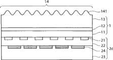
图1是表示本发明实施方式1的发光元件结构的剖视图,图2是其俯视图。在图2中,由参照符号I-I表示图1的剖面。图1是一个基片(chip)的剖面,一个基片的尺寸例如是0.3~1mm见方。图2表示图1的部分正视图。FIG. 1 is a cross-sectional view showing the structure of a light emitting element according to
如图1所示,发光元件具有包含GaN系列材料的半导体层1、以及形成于半导体层1下面的反射层2。半导体层1具有形成于反射层2上面的p型半导体层11、形成于p型半导体层11上面的发光层12、以及形成于发光层12上面的n型半导体层13。As shown in FIG. 1 , the light-emitting element has a
在n型半导体层13的上表面以规定间隔A(周期A)形成有凸部141。间隔A比从发光层12射出的光在半导体层1内的波长长。具体而言,如设从发光层12射出的光的波长为λ、半导体层1的折射率为n,则间隔A满足A≥λ/n。在图1所示的例子中,光取出一侧的面是n型半导体层13的上表面。此时,从提高光取出效率的观点出发,较为理想的是,凸部141中的凹凸的剖面形状大致为相似形。
如图2所示,凸部141从上方看的形状是圆形。即,凸部141分别具有高度相同、且半径相同的圆筒形状。As shown in FIG. 2 , the
反射层2包含相对于由发光层12发出的光的波长具有90%以上的反射率的金属等部件。这种发光元件可以利用本领域技术人员公知的MOCVD法容易地制作。The
图3是表示凹凸部14的效果的图,图3A表示未形成凹凸部14的发光元件,图3B表示形成有凹凸部14的发光元件,图3C表示将凹凸部14的凸部141的间隔A设定为光波长的10倍以上的情况。如图3A所示,在半导体层1的上表面(光取出一侧的面)S1上未形成凹凸部14的情况下,即半导体层1的上表面为平坦面的情况下,从发光层12射出的光之中以逃逸圆锥外的方向射出的光L1不被从半导体层1的上表面S1取出,而进行镜反射,被引向半导体层1的下表面S2,在下表面S2上进行镜反射,这样,在半导体层1内反复进行镜反射,永远不会进入逃逸圆锥内。因此,光取出效率降低。3 is a diagram showing the effect of the concave-
另一方面,如图3B所示,在上表面S1的表面形成具有比从发光层12射出的光的波长更长的间隔A的凹凸部14时,未从凹凸部14被取出而反射的光L1因凹凸部14而受衍射、散射的影响,以镜反射以外的方向反射到上表面S1(角度变换作用)。由此,当最初发光时以逃逸圆锥外的方向射出的光也经过多重反射而最终逃逸,从凹凸部14被取出。On the other hand, as shown in FIG. 3B , when the concave-
另外,如图3C所示,在将凹凸部14的间隔A设为从发光层12射出的光的波长的10倍以上的情况下,微观观察半导体层1时,被射出到逃逸圆锥外的光L2在点P进行镜反射,但宏观观察半导体层1时,光L2以与镜反射很大不同的方向反射到形成有凹凸部14的上表面S1,凹凸部14的角度变换作用加强。In addition, as shown in FIG. 3C , when the interval A of the concave-
图4是表示组合凹凸部14与反射层2所实现的效果的图表。在图4所示的图表中,纵轴表示光取出效率,横轴表示反射层的反射率。其中,标绘白圆○的曲线C1表示实施方式1的发光元件,该发光元件具备在半导体层1的上表面S1上形成有凹凸部14的半导体层1与反射层2,标绘黑四角◆的曲线C2表示具备在上表面S1上未形成凹凸部14的平面状的半导体层与反射层的发光元件。另外,在该图表中,利用凹凸部14的间隔A为350nm、凸部141的直径为245nm、凸部141的高度为100nm的发光元件。FIG. 4 is a graph showing the effects achieved by combining the concave-
如曲线C1所示,在实施方式1的发光元件中,反射层2的反射率从0~85%为止,光取出效率缓慢增大,但是当反射层2的反射率达到85%以上时,光取出效率急剧增大。特别是在反射层2的反射率为90%以上的区域,当反射层2的反射率增大5%时,光取出效率上升约20%。由此可知,反射层2的反射率以85%以上为宜,以90%~100%为佳,以95%~100%更佳。As shown by the curve C1, in the light-emitting element of
另一方面,如曲线C2所示,在未具备凹凸部14的发光元件中,随着反射层2的反射率增大,光取出效率呈线性增大,但是其增大率明显低于曲线C1的反射率在0~85%的区域的增大率,而且,即使反射层2的反射率达到100%,光取出效率也不足10%。由此可知即使设置有反射层2,如果没有设置凹凸部14,则光取出效率几乎不会提高。因此,在实施方式1的发光元件中,通过组合凹凸部14与反射层2所实现的相乘效果,能够大幅度地提高光取出效率。On the other hand, as shown by the curve C2, in the light-emitting element without the concave-
如所述说明的那样,实施方式1的发光元件,由于根据所述实验事实,在半导体层1的上表面S1上形成凹凸部14,并且在下表面S2上形成反射率在90%以上的反射层2,因此能够提高光取出效率。As described above, in the light-emitting element of
另外,在所述实施方式1中,半导体层1包括形成于反射层2上面的p型半导体层11、形成于p型半导体层11上面的发光层12、以及形成于发光层12上面的n型半导体层13,并在n型半导体层13的上表面以规定间隔A形成凸部141,但是半导体层1也可以包括形成于反射层2上面的n型半导体层13、形成于该n型半导体层13上面的发光层12、以及形成于该发光层12上面的p型半导体层11,并在p型半导体层11的上表面以规定间隔形成凸部141。在以下的实施方式中也同样,n型半导体层13和p型半导体层11的层叠位置可以相互交换。In addition, in
(实施方式2)(Embodiment 2)
接下来,对实施方式2的发光元件进行说明。实施方式2的发光元件的要点在于,凹凸部14的结构与实施方式1的发光元件不同。Next, the light-emitting element of
图5是从斜上方放大表示实施方式2的发光元件的凹凸部14的图。由于实施方式2的发光元件相对于实施方式1的发光元件,除凹凸部14以外,其它的结构均相同,因此省略其说明。FIG. 5 is an enlarged view showing the concavo-
如图5所示,凸部141呈六角锥形状。而且,凸部141的间隔A,以从发光层12射出的光在半导体层1内的波长的数倍(例如2倍、5倍、10倍等)为中心,在不低于所述波长的指定范围内,随机地取一定的偏差而予以排列。例如,在半导体层1包含GaN系列材料的情况下,由于折射率大约是2.5,因此若从发光层12射出波长460nm的光,则射出的光在半导体层1内的波长为184(=460/2.5)nm。因此,若凸部141的间隔A,以数百(例如500)nm为中心,在不低于184nm的范围内随机地取一定的偏差,由于未从凹凸部14取出的光,是以正反射以外的角度且取一定的偏差的角度被反射,因此能够进一步提高经多重反射之后逃逸而从凹凸部14被取出的概率。As shown in FIG. 5 , the
而且,间隔A为不规则的凸部141,可以通过利用KOH溶液(氢氧化钾溶液),边进行光照射边进行蚀刻的光辅助蚀刻,无掩膜、简易且低成本地进行制作。此外,作为凸部141的形状,从制作简单化的观点出发采用六角锥,但是并不限定于此,根据作为半导体层1而采用的材料的特性,也可以采用容易制作的形状,例如四角锥、三角锥、圆锥等。In addition, the intervals A are
如以上所说明,在实施方式2的发光元件中,由于在半导体层1的上表面S1上形成有间隔A为不规则的凸部141,因此未从凹凸部14取出的光是以各种角度被反射,因此能够进一步提高光取出效率。As described above, in the light-emitting element of
(实施方式3)(Embodiment 3)
接下来,对实施方式3的发光元件进行说明。图6是表示实施方式3的发光元件的结构的剖视图。如图6所示,实施方式3的发光元件的要点在于,使半导体层1的上表面S1的形状设为具有透镜作用的形状。所谓透镜作用,是指如凸透镜或凹透镜那样聚光或发散的作用。在实施方式3中,对与实施方式1、2相同的结构标注相同的附图标记,并省略其说明。更具体而言,在图6所示的例子中,要点在于,构成凹凸部14a的各凸部141a的形状设为凸透镜状。另外,凸部141a的间隔A,与实施方式1同样地,如设从发光层12射出的光的波长为λ、半导体层1的折射率为n时,A≥λ/n。Next, the light-emitting element of Embodiment 3 will be described. 6 is a cross-sectional view showing the structure of a light emitting element according to Embodiment 3. FIG. As shown in FIG. 6 , the point of the light-emitting element of Embodiment 3 is that the shape of the upper surface S1 of the
这样,通过将凸部141a的形状制成凸透镜状,能够控制从凹凸部14a取出的光的配光,提供适宜作为照明器具的发光元件的发光元件。其中,凸部141a的形状不限定于凸透镜状,可以根据希望如何控制从凹凸部14a取出的光的配光来适当变更。In this way, by making the shape of the
例如,凸部141a的形状,也可替代图6所示的凸透镜状,采用如图7所示的菲涅耳透镜(Fresnel lens)形状。图7表示将凸部141a制成菲涅耳透镜形状的情况下的凸部141a的俯视图。图8表示沿着由参照符号VIII-VIII表示的线切断图7所示的凸部141a的情况下的发光元件的剖视图。For example, instead of the convex lens shape shown in FIG. 6, the shape of the
在此,构成图8所示的菲涅耳透镜的小透镜部142a,如图9(a)所示,也可以由具有半径互不相同的多个细微的圆筒状凸部143a的子波长衍射光栅(sub-wavelengthdiffractive lattice)构成。图9(a)是表示子波长衍射光栅的详细结构的图,图9(b)是图9(a)的俯视图,图9(c)是图9(b)的区域D1的放大图。Here, the
如图9(b)所示,凸部143a的半径根据小透镜部142a的表面相对于水平面的斜率而变更。更具体而言,随着小透镜部142a表面的斜率变平缓而凸部143a的半径也变大。凸部143a的半径小于从发光层12射出的光在半导体层1内的波长。这样,即使由图9(a)~(c)所示的子波长衍射光栅构成图8所示的菲涅耳透镜,也能够起到与菲涅耳透镜相同的作用。As shown in FIG. 9( b ), the radius of the convex portion 143a is changed according to the slope of the surface of the
另外,如图10所示,也可以由区板构成图7所示的凸部141a。此外,实施方式3所示的凹凸部14a可以通过众所周知的热回流(thermal reflow)法、纳米印刷(nanoprint)法而容易地实现。In addition, as shown in FIG. 10, the
如以上所说明,在实施方式3的发光元件中,由于凸部141a被设为具有透镜作用的形状,因此能够提供适用于照明设备的发光元件。另外,通过将凸部141a设为菲涅耳透镜形状、子波长衍射光栅形状、区板形状,能够在不增加凸部141a的厚度的状态下控制透过凸部141a的光的焦点距离。As described above, in the light emitting element of Embodiment 3, since the
(实施方式4)(Embodiment 4)
接下来,对实施方式4的发光元件进行说明。实施方式4的发光元件的要点在于,作为构成实施方式1~3的发光元件的反射层2的部件,采用以银为主成分的合金(银合金)。特别是,在实施方式4中,作为反射层2采用AgPdCu系银合金。从提高反射率的观点出发,作为反射层2采用Ag为宜。但Ag相对于GaN的电传导性较差,而且Ag容易氧化,因此采用相对于GaN的电传导性良好且不易氧化的银合金更佳。Next, the light-emitting element of
如以上所说明,在实施方式4的发光元件中,由于作为反射层2采用了银合金,因此反射层2具有高反射率、且相对于GaN的电传导性良好,能够提供一种光取出效率高的发光元件。As described above, in the light-emitting element of
(实施方式5)(Embodiment 5)
接下来,对实施方式5的发光元件进行说明。图11是表示实施方式5的发光元件的结构的剖视图。如图11所示,实施方式5的发光元件的要点在于,作为实施方式1~4的发光元件的反射层2,采用包括白金层21、导电性氧化物层22、以及金属层23的反射层2a。Next, the light emitting element of
图11所示的发光元件,具有包含GaN系列材料的半导体层1、以及形成于半导体层1表面的反射层2a。The light-emitting element shown in FIG. 11 has a
半导体层1包括形成于反射层2a表面的p型半导体层11、形成于p型半导体层11表面的发光层12、以及形成于发光层12表面的n型半导体层13。在n型半导体层13的表面上以规定间隔A(周期A)形成有凸部或凹部141。间隔A比从发光层12射出的光在半导体层1内的波长长。具体而言,如设从发光层12射出的光的波长为λ、半导体层1的折射率为n,则间隔A满足A≥λ/n。在图11所示的例子中,光取出一侧的面是n型半导体层13的上表面。The
反射层2a是相对于由发光层12发出的光的波长具有90%以上的反射率的层,在本实施方式中,包括白金层21、导电性氧化物层22、以及金属层23。
白金层21包含俯视观察呈网状或岛状(island-like shape)的白金(Pt)层,其被形成于半导体层1中的p型半导体层11的面上。岛的形状,例如,俯视观察呈椭圆形(包含圆形)、四角形、六角形等多角形等。白金层21用于确保p型半导体层11与导电性氧化物层22之间的电连接。The
导电性氧化物层22,是例如由ITO(Indium Tin Oxide)、ZnO等具有导电性、相对于发光层12发出的光的波长呈透明的金属氧化物构成的层。由于白金层21呈网状或岛状,因此导电性氧化物层22以其一部分与半导体层1的p型半导体层11接触的状态形成于白金层21的表面。换言之,以网状或岛状的白金层21介于半导体层1的p型半导体层11与导电性氧化物层22之间的状态,导电性氧化物层22形成于半导体层1的p型半导体层11的表面。导电性氧化物层22介于半导体层1的p型半导体层11与金属层23之间,使得接触电阻降低,导电性即载流子注入效率提高。The
金属层23例如是包含银(Ag)、以银为主成分的银合金、铝(Al)或以铝为主成分的合金(铝合金)等金属(包含合金)的层。为了维持金属层23中的较高的反射率,导电性氧化物层22与半导体层1接触的面积(开口率)在80%以上为宜。The
这种反射层2a,在某实施例中,例如白金层21设为1.5nm以下,导电性氧化物层22设为5nm以下的ITO,金属层23设为300nm的银。并且,虽图中未表示,在银的金属层23的下面形成作为衬底层的厚度30nm的镍(Ni)层和厚度1000nm的金(Au)层,以将其作为电极衬垫。In a certain embodiment, the
如以上所说明,在具有这种结构的发光元件中,由于采用包括白金层21、导电性氧化物层22以及金属层23的反射层2a,因此能够提供一种金属层23具有高反射率且与p型半导体层11欧姆接触、光取出效率高的发光元件。例如,在所述某实施例中,反射层2a显示大约91.5%的反射率,通过与形成于n型半导体层13上表面的凹凸部14的相乘效果,可以获得大约60%以上的光取出效率。As explained above, in the light-emitting element having such a structure, since the
此外,在所述实施方式中,为了实现更好的欧姆接触,也可以在p型半导体层11中添加例如镁(Mg)等p型掺杂剂(p-type dopant)。In addition, in the above embodiment, in order to achieve better ohmic contact, a p-type dopant (p-type dopant) such as magnesium (Mg) may also be added to the p-
(实施方式6)(Embodiment 6)
接下来,对实施方式6的发光元件进行说明。图12是表示实施方式6的发光元件的结构的剖视图。如图12所示,实施方式6的发光元件的要点在于,作为实施方式1~4的发光元件的反射层2,采用由DBR(distributed bragg reflector)构成的反射层2b。在实施方式6中,与实施方式1~4相同的结构标注同一附图标记,并省略其说明。在本实施方式中,DBR是将多个具有从发光层12射出的光在半导体层1内的波长的1/4的厚度、折射率互不相同的层重叠来构成的反射镜。在DBR中,通过光的干扰效果引起的布拉格反射(Bragg reflection),各层中的反射波相互增强,由此能够得到较高的反射率。在本实施方式中,采用层叠了50对AlGaN/GaN成对层的DBR。由此,反射层2能够实现99%以上的反射率。这样的DBR例如可通过电子束(EB)的蒸镀而形成。Next, a light emitting element according to Embodiment 6 will be described. 12 is a cross-sectional view showing the structure of a light emitting element according to Embodiment 6. FIG. As shown in FIG. 12 , the point of the light-emitting element of the sixth embodiment is that a
DBR可实现接近100%的反射率,在公知的DBR中,将相对于以图12所示的AB面的法线方向入射的光、即以入射角0度入射的光的反射率设为100%。这是由于,构成DBR的各层的层厚d1被设定为入射的光的波长的1/4。DBR can achieve a reflectance close to 100%. In the known DBR, the reflectance of light incident in the direction normal to the AB surface shown in FIG. %. This is because the layer thickness d1 of each layer constituting the DBR is set to 1/4 of the wavelength of incident light.
然而,如图13A所示,从发光层12射出的光的配光分布随着入射角从0度接近90度,光束增大。另外,如图13B所示,按照凹凸部14的形状,入射角与经凹凸部14的透过率之间的关系也不同。However, as shown in FIG. 13A , the light distribution of the light emitted from the
图13A是表示从发光层12射出的光的配光分布的图表,纵轴表示光束(lm)的相对强度,横轴表示角度(deg)。其中,角度表示来自发光层12的光相对于法线方向的角度。如图13A所示,从发光层12射出的光束随着角度变大而增大。13A is a graph showing the light distribution of light emitted from the light-emitting
图13B是表示对应于凹凸部14形状的透过特性的图表,纵轴表示经凹凸部14的透过率(光取出效率),横轴表示入射到上表面S1的入射角。另外,在图13B中,曲线C31表示使凹凸部14的剖面形状为平面状的情况,曲线C32表示使凹凸部14的剖面形状为三角波状的情况,曲线C33表示使凹凸部14的剖面形状为正弦波状的情况,曲线C34表示使凹凸部14的剖面形状为方形波状的情况,曲线C35表示使凹凸部14的形状为圆状的情况,并且,曲线C36表示使凹凸部14的剖面形状为研钵状的情况。13B is a graph showing transmission characteristics corresponding to the shape of the concave-
如图13B所示,根据凹凸部14的形状的不同,光的透过特性会有很大的不同。在此,一次透过情况下的光取出效率一般由下式表示:As shown in FIG. 13B , depending on the shape of the concavo-
光取出效率η=∫(透过率(θ)×配光分布(θ))dθLight extraction efficiency η=∫(transmittance (θ)×light distribution (θ))dθ
因此,实际上从凹凸部14取出到外部的光量为图13A所示的曲线与图13B所示的曲线C31~C36中的任一条曲线相重叠的区域。Therefore, the amount of light actually taken out from the concavo-
例如,在示意图13B中的方形波的曲线C34中,以相对于在光束强度较大的范围,且在透过率较低的角度,即从30度到90度的范围内的中间角度60度,使DBR的反射率成为99%以上的方式,设计DBR即可。如图14所示,这可以通过以使相对于法线方向成角度(θ=60度)的直线上的各层的长度为从发光层12射出的光在半导体层1中的波长λ’的1/4的方式,设定DBR的层厚d1来实现。由此能够使从30度到90度的透过率增大,从而增大光取出效率。For example, in the curve C34 of the square wave in the schematic diagram 13B, the middle angle of 60 degrees relative to the range where the beam intensity is larger and the transmittance is lower, that is, the range from 30 degrees to 90 degrees , The DBR may be designed so that the reflectance of the DBR becomes 99% or more. As shown in FIG. 14 , this can be achieved by making the length of each layer on a straight line at an angle (θ=60 degrees) with respect to the normal direction equal to the wavelength λ' of the light emitted from the light-emitting
另外,在图13B表示的三角形波的曲线C32的情况下,以使透过率较低的70度附近的光的反射率成为99%以上的方式设计DBR即可。这如图14所示,可以通过以使相对于法线方向成角度(θ=70度)的直线上的各层中的长度成为从发光层12射出的光在半导体层1中的波长λ’的1/4的方式,设定DBR的层厚d1来实现。此外,在曲线C32上,由于角度40度附近的透过率也较低,因此还可以考虑以使角度40度附近的光的反射率提高的方式设计DBR。然而,如图13A所示,由于与角度40度附近相比角度70度附近的光束的值较大,因此为了提高光取出效率,较为理想的是,以使角度70度附近的反射率提高的方式设计DBR。In addition, in the case of the curve C32 of the triangular wave shown in FIG. 13B , it is only necessary to design the DBR so that the reflectance of light near 70 degrees, where the transmittance is low, becomes 99% or more. This can be done by making the length of each layer on a straight line at an angle (θ=70 degrees) with respect to the normal direction to be the wavelength λ' of the light emitted from the light-emitting
如以上所说明,在实施方式6的发光元件中,由于反射层2b由DBR构成,因此反射层2b的反射率提高,光取出效率进一步提高。而且,在按照凹凸部14的形状而决定的透过特性方面,由于以使透过率较低的角度的光在DBR中的反射率提高的方式设定DBR的层厚,因此可降低一次透过还没有完全透过的光由于多重反射所引起的损失,进一步提高光取出效率。As described above, in the light-emitting element of Embodiment 6, since the
(实施方式7)(Embodiment 7)
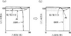
接下来,对实施方式7的发光元件进行说明。图15是表示实施方式7的发光元件的结构的剖视图。如图15所示,实施方式7的发光元件的要点在于,作为实施方式1~4的发光元件的反射层2,采用反射层2c,该反射层2c具有:包括铝、银或银合金的金属层23、以及层叠于该金属层23上的DBR24。在该反射层2c的DBR24上形成半导体层1。即,实施方式7的发光元件是在实施方式6的发光元件的DBR的下面进一步层叠金属层的结构。在实施方式7中,与实施方式1~4相同的结构标注同一附图标记,并省略其说明。Next, the light emitting element of Embodiment 7 will be described. 15 is a cross-sectional view showing the structure of a light emitting element according to Embodiment 7. FIG. As shown in FIG. 15 , the point of the light-emitting element of Embodiment 7 is that, as the
图16是表示银或银合金(银/银合金)和DBR的入射角与反射率之间的关系、以及铝(Al)和DBR的入射角与反射率之间的关系的反射率特性图表。图16的纵轴表示反射率(%),横轴表示入射角。在图16(a)中,实线表示银或银合金的反射率特性,点划线表示铝的反射率特性,另外,双点划线表示DBR的反射率特性。如图16(a)所示,银或银合金的反射率以及铝的反射率在入射角从0度到75度左右为止低于DBR,但是从超过75度左右开始高于DBR。此外,银或银合金的反射率高于铝的反射率。16 is a reflectance characteristic graph showing the relationship between the incident angle and the reflectance of silver or silver alloy (silver/silver alloy) and DBR, and the relationship between the incident angle and reflectance of aluminum (Al) and DBR. In FIG. 16 , the vertical axis represents the reflectance (%), and the horizontal axis represents the incident angle. In FIG. 16( a ), the solid line represents the reflectance characteristics of silver or silver alloy, the dashed-dotted line represents the reflectance characteristics of aluminum, and the dashed-two dotted line represents the reflectance characteristics of DBR. As shown in FIG. 16( a ), the reflectance of silver or silver alloy and that of aluminum are lower than DBR when the incident angle is from 0° to about 75°, but higher than DBR when the incident angle exceeds about 75°. Furthermore, the reflectivity of silver or silver alloys is higher than that of aluminum.
因此,在构成如图15所示那样的反射层2c的情况下,反射层2c具有图16(b)所示的将DBR的反射率特性与银或银合金的反射率特性合成的反射率特性,或者,具有图16(b)所示的将DBR的反射率特性与铝的反射率特性合成的反射率特性。Therefore, in the case of configuring the
其结果,能够构成相对于全入射角具有较高的反射率的反射层2c。此外,通常DBR由多个成对的层(pair layers)构成,但作为特殊情况,在层叠所述高反射的金属层与DBR的反射层2c中,DBR的层数也可以是一层。As a result, the
对于这种反射层2c的反射率的角度依赖性进行了模拟实验。图17是表示在模拟实验中利用的反射层2c的结构的图。图18是表示反射层2c的反射率的角度依赖性的模拟实验结果。图18的纵轴表示强度反射率,横轴表示从GaN向DBR的入射角。C41表示由DBR24与银的金属层23构成的反射层2c的情况下的反射率,C42表示由DBR构成的反射层2b的情况下的反射率。A simulation experiment was carried out on the angular dependence of the reflectance of the
如图17所示,在模拟实验中利用的反射层2c在作为p型半导体层11的GaN层上层叠DBR24,在DBR24上层叠厚度300nm的由银构成的金属层23。DBR24层叠有15层TiO2与MgF2成对层,还层叠有TiO2。为了能设置成波长λ(=460nm)的1/4n,TiO2的折射率为2.24,其膜厚设为51.34nm,MgF2的折射率为1.38,其膜厚设为83.33nm。银的复折射率为0.055-3.32i(i为虚数单位)。As shown in FIG. 17 , in the
由图18可知,在反射层2是由DBR构成的反射层2b的情况下,在入射角为从大约17度到大约50度的范围以及从大约60度到大约90度的范围内,显现反射率的下降。另一方面,在反射层2是由DBR和银的金属层构成的反射层2c的情况下,在从0度到90度的整个入射角范围内几乎都看不到反射率的降低,保持大约95%以上的反射率。As can be seen from FIG. 18, in the case where the
如以上所说明,在实施方式7的发光元件中,由于反射层2c由DBR24与金属层23构成,因此各层相互弥补,在从0度到90度的大范围的入射角下,提高反射层2c的反射率,光取出效率进一步提高。As described above, in the light-emitting element of Embodiment 7, since the
(实施方式8)(Embodiment 8)
接下来,对实施方式8的发光元件进行说明。图19是表示实施方式8的发光元件的结构的剖视图。如图19所示,实施方式8的发光元件的要点在于,作为实施方式1~4的发光元件的反射层2,采用包括白金层21、导电性氧化物层22、金属层23、以及DBR24的反射层2d。在该反射层2d的白金层21上形成半导体层1。在实施方式8中,与实施方式1~4相同的结构标注同一附图标记,并省略其说明。Next, a light-emitting element according to Embodiment 8 will be described. 19 is a cross-sectional view showing the structure of a light emitting element according to Embodiment 8. FIG. As shown in FIG. 19, the point of the light-emitting element of Embodiment 8 is that, as the
反射层2d是相对于由发光层12发出的光的波长具有90%以上的反射率的层,在本实施方式中,包括白金层21、导电性氧化物层22、金属层23、以及DBR24。白金层21以及导电性氧化物层22与实施方式5的发光元件的白金层21以及导电性氧化物层22相同,省略其说明。
DBR24与实施方式7的发光元件的DBR24相同,在本实施方式8中,从上方观察呈网状或岛状,形成于导电性氧化物层22的下表面。岛的形状例如从上方观察呈椭圆形(包含圆形)以及四角形、六角形等多角形等。如此,由于DBR24形成为网状或岛状,因此,即使在DBR24的导电率较低的情况下,也能够确保导电性氧化物层22与金属层23之间的电传导。此外,在确保导电性氧化物层22与金属层23之间的电传导方面DBR24具有充分的导电率的情况下,DBR24也可以形成于导电性氧化物层22与金属层23的整个界面上。The
金属层23与实施方式7的发光元件的金属层23相同,由于在本实施方式8中DBR24呈网状或岛状,因此金属层23以其一部分与导电性氧化物层22接触的状态形成于DBR24的下面。换言之,以网状或岛状的DBR24介于导电性氧化物层22与金属层23之间的状态,金属层23形成于导电性氧化物层22的下面。The
这种反射层2d在某实施例中例如为,白金层21设为1.5nm以下、导电性氧化物层22设为5nm以下的ITO、金属层23设为300nm的银、DBR24设为层叠有15组TiO2与MgF2构成的组并且最后层叠有TiO2的反射镜。另外,虽图中未表示,但在银的金属层23的下面形成作为衬底层的厚度30nm的镍(Ni)层和厚度1000nm的金(Au)层,以使其作为电极衬垫。Such a
对于这种反射层2d的反射率的角度依赖性进行模拟实验。图20是表示在模拟实验中利用的反射层2d的结构的图。图21是表示反射层2d的反射率的角度依赖性的模拟实验结果。图21的纵轴表示强度反射率,横轴表示从GaN向DBR的入射角度。C51表示由DBR24与银的金属层23构成的反射层2c的情况下的反射率,C52及C53表示由ITO的导电性氧化物层22、DBR24、以及银的金属层23构成的反射层2d的情况下的反射率。C52表示ITO的膜厚为5nm的情况,C53表示ITO的膜厚为50nm的情况。A simulation experiment was carried out on the angular dependence of the reflectivity of such a
如图20所示,在模拟实验中利用的反射层2d在作为p型半导体层11的GaN层上形成ITO的导电性氧化物层22,在导电性氧化物层22上形成DBR24,在DBR24上形成厚度300nm的由银构成的金属层23。关于ITO,分别对膜厚为5nm的情况以及50nm的情况进行了模拟实验,其复折射率为2.3-0.008i。DBR24层叠有15层TiO2与MgF2成对层,还层叠有TiO2。为了设置为波长λ(=460nm)的1/4n,TiO2的折射率为2.24,其膜厚设为51.34nm。即,图20所示的反射层2d相对于图17所示的反射层2c,是ITO介于GaN与DBR之间的结构。As shown in FIG. 20, the
由图21可知,在反射层2是包含ITO的反射层2d的情况下,由于ITO吸收一点光,因此与反射层2是不包含ITO的反射层2c的情况相比,反射率一定程度地降低,但是在从0度到90度的整个入射角范围内均可保持良好的反射率。ITO的膜厚越薄,整体反射率越好。特别是,在ITO的膜厚是5nm的情况下,在从0度到90度的整个入射角范围内均保持大致90%以上的反射率。另外,即使在ITO的膜厚是50nm的情况下,在从0度到70度的整个入射角范围内均保持大致90%以上的反射率。As can be seen from FIG. 21 , when the
如以上所说明,在这种结构的发光元件中,由于采用由白金层21、导电性氧化物层22、金属层23以及DBR24构成的反射层2d,因此能够提供在从0度到90度的大范围的入射角下反射层2d的反射率均提高、并且反射层2d与p型半导体层11欧姆接触、光取出效率更高的发光元件。As explained above, in the light-emitting element of this structure, since the
此外,在所述实施方式中,DBR24也可以是构成DBR的各成对层的膜厚、折射率逐渐变化的线性(chirp)DBR。通过采用线性DBR结构,可以减少在DBR中的反射率波动,即射入DBR结构的光在特定波长域、角度域内局部发生的反射率的降低,整体的反射率提高。在反射层2d的情况下,DBR的层数也可以是一层。In addition, in the above-described embodiment, the
(实施方式9)(Embodiment 9)
接下来,对实施方式9的发光元件进行说明。图22是表示实施方式9的发光元件的结构的剖视图。实施方式9的发光元件的要点在于,作为反射层2e采用光子晶体(photoniccrystal)。光子晶体能够对各种入射角度实现大致100%的反射率。在实施方式9中,与实施方式1~4相同的结构标注同一附图标记,并省略其说明。Next, a light-emitting element according to Embodiment 9 will be described. FIG. 22 is a cross-sectional view showing the structure of a light emitting element according to Embodiment 9. FIG. The point of the light-emitting element of Embodiment 9 is that a photonic crystal is used as the
图23是作为光子晶体采用了反蛋白石结构(inverse opal structure)的光子晶体的情况下的反射层2e的放大图。如图23所示,三维光子晶体的要点在于,包含多个泡状排列的球形空洞。该空洞的间距为从发光层12射出的光在半导体层1内的波长的大约1/2。更具体而言,如果作为半导体层1采用GaN,并从发光层12射出460nm的光,由于GaN的折射率大约是2.5,因此空洞的间距设为(460/2.5)×(1/2)=大约100nm较为理想。FIG. 23 is an enlarged view of the
具有该反蛋白石结构的光子晶体可以通过公知的反蛋白石法容易制成。在该反蛋白石法中,首先层叠相当于空洞的微粒子。接下来,层叠的微粒子被浸入到有机溶剂中。并且,将该有机溶剂烧固,使有机溶剂碳化之后,将微粒子熔化。由此,形成反蛋白石结构。此外,碳具有导电性,因此即使不另外形成电极,也可将光子晶体直接用作为电极。Photonic crystals having this inverse opal structure can be easily produced by the known inverse opal method. In this inverse opal method, first, fine particles corresponding to cavities are stacked. Next, the stacked microparticles are immersed in an organic solvent. Then, the organic solvent is baked to carbonize the organic solvent, and then the fine particles are melted. Thus, an inverse opal structure is formed. In addition, carbon has conductivity, so photonic crystals can be directly used as electrodes without forming electrodes separately.
另外,在实施方式9中,作为反射层2e中采用的光子晶体,也可以采用多孔(porous)Si光子晶体(二维光子晶体)。图24是多孔Si光子晶体的剖视图。如图24所示,二维光子晶体具有管状空洞排列为矩阵状的结构。其中,半导体层1以与所述管状空洞的长边方向正交的方向平行于半导体层1的上表面S1的状态,层叠在多孔硅Si光子晶体上。In addition, in Embodiment 9, a porous (porous) Si photonic crystal (two-dimensional photonic crystal) may be used as the photonic crystal used in the
在此,可以通过贴合多孔Si光子晶体与GaN来制作发光元件,但也可以通过将多孔Si光子晶体作为生长基板(growing substrate),生长GaN来制作发光元件。这样,可省略多孔Si光子晶体与GaN的贴合步骤,并且可提高GaN的质量,提高发光元件内部的量子效率。Here, a light-emitting device can be produced by laminating porous Si photonic crystals and GaN, but it is also possible to produce a light-emitting device by growing GaN using a porous Si photonic crystal as a growing substrate. In this way, the bonding step of the porous Si photonic crystal and GaN can be omitted, the quality of GaN can be improved, and the quantum efficiency inside the light-emitting element can be improved.
多孔Si光子晶体中,相对于空洞的长边方向即法线方向不存在光子晶体带(photonicband),因此反射率稍有减弱,但是由于在相对于法线方向倾斜的方向上具有光子晶体带,因此对于该方向的光可实现较高的反射率。另外,由于多孔Si光子晶体具有导电性,因此可直接用作为电极。In the porous Si photonic crystal, there is no photonic crystal band (photonic band) relative to the long side direction of the hole, that is, the normal direction, so the reflectivity is slightly weakened, but since there is a photonic crystal band in the direction inclined relative to the normal direction, A higher reflectivity can thus be achieved for light in this direction. In addition, porous Si photonic crystals can be directly used as electrodes due to their electrical conductivity.
此外,在实施方式9中,作为在反射层2e中采用的光子晶体,也可以采用通过倾斜转动蒸镀法(GLAD、glancing angle deposition)制作的光子晶体。图25表示通过倾斜转动蒸镀法制作的光子晶体的放大图。倾斜转动蒸镀法是以指定周期转动倾斜的生长基板,使光子晶体在生长基板上生长为螺旋状的手法。In addition, in the ninth embodiment, as the photonic crystal used in the
如以上所说明,在实施方式9的发光元件中,由于采用了由光子晶体构成的反射层2e,因此能够实现对于任何入射角度均具有高反射率的反射层2e,能够提高光取出效率。As described above, since the
(实施方式10)(Embodiment 10)
接下来,对实施方式10的发光元件进行说明。图26是表示实施方式10的发光元件的结构的剖视图。实施方式10的发光元件的要点在于,相对于实施方式1~9的发光元件,将半导体层1的厚度,即半导体层1的包含凹凸部14底部的面S1与下表面S2之间的距离d2,设为从发光层12射出的光在半导体层1内的波长的数倍以内。在实施方式10中,与实施方式1~9相同的结构标注同一附图标记,并省略其说明。图27是立体表示从发光层12射出的光的发光分布的图。如图27所示,从发光层12射出的光如图中涂黑所示,法线方向的成分最多。然而,法线方向的光,由于凸部141的上表面与法线方向直交,因此有可能不能受到凹凸部14的角度变换作用。Next, the light emitting element of
于是,将距离d2设为从发光层12射出的光的波长的数倍,较为理想的是1~5倍,更为理想的是与所述波长相同,由此法线方向的光也可受到凹凸部14的角度变换作用,可以进一步提高光取出效率。具体而言,如设来自发光层12的光的波长为460nm、半导体层1的折射率为2.5,则距离d2设为180nm~1000nm较为理想。Therefore, the distance d2 is set to be several times the wavelength of the light emitted from the
如以上所说明,在实施方式10的发光元件中,距离d2设为波长的数倍或大致与其相同,因此能够进一步提高光取出效率。As described above, in the light-emitting element of
(实施方式11)(Embodiment 11)
接下来,对实施方式11的发光元件进行说明。图28是表示实施方式11的发光元件的结构的剖视图。图28A表示发光元件是纵型的情况,图28B表示发光元件是倒装片(flipchip)型的情况。实施方式11的发光元件的要点在于,对于实施方式1~10的发光元件,设置向半导体层1的发光层12提供电力的p型及n型电极,并且,n型电极也采用高反射率的电极。在实施方式11中,与实施方式1~10相同的结构标注同一附图标记,并省略其说明。Next, the light emitting element of
在向半导体层1的发光层12提供电力的情况下,有纵列型和倒装片型(以下简称为“FC型”),在纵列型中,一组p型及n型电极夹着发光层12相对设置,在倒装片型中,一组p型及n型电极相对于发光层12设置于同一侧。In the case of supplying power to the light-emitting
所述纵列型的发光元件,例如如图28A所示,将实施方式1~10的发光元件中的反射层2(2a~2e)作为p型电极,在半导体层1中的n型半导体层13的上面形成n型电极5,作为p型电极的反射层2(2a~2e)与n型电极5夹着发光层12相对设置。并且,在该纵列型的发光元件中,用于向作为p型电极的反射层2(2a~2e)施加正侧电压(+侧电压)的布线金属层3形成于反射层2(2a~2e)的下面,用于支撑所述半导体层1、反射层2(2a~2e)及布线金属层3的支撑层4设置于布线金属层3的下面。The tandem light-emitting element, for example, as shown in FIG. 28A , uses the reflective layer 2 (2a-2e) in the light-emitting element of
另外,FC型的发光元件中,例如如图28B所示,将实施方式1~10的发光元件中的反射层2(2a~2e)作为p型电极,并且,相对于发光层12,在形成有反射层2(2a~2e)的一侧去除发光层12、p型半导体层11、及反射层2(2a~2e),以在使半导体层1中的n型半导体层13面对外部的状态形成外露面(或者以形成所述外露面的状态形成n型半导体层13、发光层12及p型半导体层11,并在该p型半导体层11的下面形成反射层2(2a~2e)),在该外露面上形成n型电极5,p型及n型电极相对于发光层12被设置于同一侧。并且,在该FC型的发光元件中,用于向作为p型电极的反射层2(2a~2e)施加正侧电压(+侧电压)的布线金属层31形成于反射层2(2a~2e)的下面,并且用于向n型电极5施加负侧电压(-侧电压)的布线金属层32形成于n型电极5的下面,用于支撑所述半导体层1、反射层2(2a~2e)及布线金属层31、32的支撑层4设置在布线金属层31、32的下面。In addition, in an FC-type light-emitting element, for example, as shown in FIG. 28B , the reflective layers 2 ( 2 a to 2 e ) in the light-emitting elements of
图29是表示n型电极5的结构的剖视图。作为在所述纵列型或FC型的发光元件中使用的n型电极5,如图29A所示,例如采用由白金层51、导电性氧化物层52、以及金属层53构成的、具有80%以上的反射率的n型电极5a。FIG. 29 is a cross-sectional view showing the structure of n-
白金层51是由白金(Pt)构成的层,从上方观察呈网状或岛状,该白金层51形成于半导体层1中的n型半导体层13的表面。岛的形状例如从上方观察呈椭圆形(包含圆形)以及四角形、六角形等多角形等。
导电性氧化物层52是例如由ITO、ZnO等具有导电性、相对于发光层12发出的光的波长透明的金属氧化物构成的层。由于白金层51呈网状或岛状,因此导电性氧化物层52以其一部分与半导体层1的n型半导体层13接触的状态形成于白金层51的表面。换言之,以网状或岛状的白金层51介于半导体层1的n型半导体层13与导电性氧化物层52之间的状态,导电性氧化物层52形成于半导体层1的n型半导体层13的表面。由于导电性氧化物层52介于半导体层1的n型半导体层13与金属层53之间,使得接触电阻降低,导电性即载流子注入效率提高。The
金属层53是例如包括银、以银为主成分的银合金、铝或以铝为主成分的铝合金等金属(包含合金)的层。为了维持金属层53中的较高的反射率,导电性氧化物层22与半导体层1接触的面积(开口率)在80%以上为宜。The
这种n型电极5a,在某实施例中,例如白金层51设为1nm以下,导电性氧化物层52设为5nm以下的ITO,金属层53设为300nm的银。并且,虽图中未表示,但在银的金属层53的表面形成作为衬底层的厚度30nm的镍(Ni)层和厚度1000nm的金(Au)层,以使其作为电极衬垫。For such an n-
或者,作为在所述纵列型或FC型的发光元件中利用的n型电极5,例如也可以采用n型电极5b,该n型电极5b,如图29B所示,在图29A所示的n型电极5a中的导电性氧化物层52与金属层53之间进一步设置与实施方式6、实施方式7中的DBR24相同的DBR54。另外,该DBR54也可以如同实施方式8中的DBR24,从上方观察呈网状或岛状。Alternatively, as the n-
一般而言,n型电极由反射率相对较低的例如镍(Ni)等金属形成,在提高光取出效率方面,没有考虑到反射率。特别是,在FC型中,由于仅在与形成有p型电极的区域对应的发光层12的区域发光,因此被认为n型电极的反射率不贡献于光取出效率的提高。通常,由于n型电极的面积是元件整体面积的大约10%,因此如n型电极的反射率相对较低,例如为30%左右,则即使将p型电极的反射率提高至85%以上,发光元件的平均反射率也变为80%左右。因此,在取出在发光元件内进行多重反射的光方面,低反射率的n型电极妨碍光取出效率的提高。In general, the n-type electrode is formed of a metal such as nickel (Ni) with relatively low reflectance, and the reflectance is not taken into consideration when improving the light extraction efficiency. In particular, in the FC type, since light is emitted only in the region of the
因此,通过将n型电极设为例如图29所示的n型电极5a、5b那样的具有80%以上的反射率的电极,能够提高发光元件的平均反射率。Therefore, the average reflectance of the light-emitting element can be increased by making the n-type electrode an electrode having a reflectance of 80% or more such as the n-
如以上所说明,在所述结构的发光元件中,由于采用包括白金层51、导电性氧化物层52以及金属层53的n型电极5a、5b,因此能够提供金属层53具有高反射率、并且与n型半导体层13欧姆接触、光取出效率高的发光元件。并且,在采用进一步具备DBR54的n型电极5b的情况下,能够提供光取出效率更高的发光元件。As described above, in the light-emitting element of the above structure, since the n-
此外,在所述n型电极5a、5b的情况下,为了降低与n型半导体层13的接触电阻,也可以在金属层53中利用包含硅(Si)、铜(Cu)、碲(Te)、锗(Ge)及锡(Sn)中的一种以上n型掺杂剂(dopant)物质的银合金或铝合金。作为金属层53,例如可采用日立金属公司制ATD系银合金。In addition, in the case of the n-
接下来,对在半导体层1上蒸镀实施方式1的凹凸部14的情况下的发光元件的制作方法进行说明。图30是表示蒸镀凹凸部14的情况下的制作方法的图。首先,在半导体层1的上表面涂敷阻膜(resist)R1(图30A)。然后,通过曝光及显影或纳米印刷法,在所涂敷的阻膜R1上形成相当于凹凸部14的形状(图30B)。接下来,在形成形状的阻膜R1上蒸镀具有与半导体层1大致相同的折射率的材料(图30C)。在本实施方式中,在阻膜R1上蒸镀具有与作为半导体层1被利用的GaN的折射率大致相同的折射率的TiO2。接着,去除阻膜(图30D)。由此,能够在半导体层1上蒸镀凹凸部14。Next, a method of manufacturing a light-emitting element in the case where the concave-
如凹凸部14那样的形成于半导体面上的细微结构,也可以通过干法蚀刻(dryetching)等蚀刻方法形成,但是用于实现蚀刻的装置非常昂贵。因此,如图30所示,在半导体层1上蒸镀具有与半导体层1大致相同的折射率的部件来形成凹凸部14,由此无需利用昂贵的蚀刻装置,能够低成本地形成凹凸部14。The fine structure formed on the semiconductor surface such as the concavo-
(实施方式12)(Embodiment 12)
接下来,对实施方式12的发光装置进行说明。图31是表示实施方式12的发光装置的结构的剖视图。实施方式12的发光装置是利用实施方式1~11的发光元件的放射白色光的装置。Next, a light emitting device according to
实施方式12的发光装置,如图31所示,在圆板状的基板61上载置实施方式11的发光元件,在该发光元件的光取出面上形成用于将该发光元件发出的光的波长变换并放射的波长变换层62,这些被密封部件63密封。In the light-emitting device of
基板61的载置发光元件的面设为高反射率,以将从发光元件放射的光高效地反射到密封部件63。基板61例如由银、铝等高反射率的金属(包含合金)形成。The surface of the
在图31所示的例子中,该实施方式11的发光元件为FC型。其支撑层4兼用作放射发光层12产生的热的散热器。并且,布线金属层31、32采用金突起。该实施方式11的发光元件例如对于蓝色的波长460nm具有发光峰值。该实施方式11的发光元件也可以是纵列型。In the example shown in FIG. 31 , the light emitting element of
由于本实施方式的发光装置放射白色光,因此波长变换层62由包含绿色荧光体和红色荧光体的荧光体分散玻璃(phosphors dispersing glass)构成,所述绿色荧光体主要吸收波长460nm附近的蓝色光,并以荧光方式发出绿色光,所述红色荧光体主要吸收波长460nm附近的蓝色光,并以荧光方式发出红色光。作为绿色荧光体,例如采用SrGa2S4:Eu2+或Y3(Al,Ga)5O12:Ce3+等。作为红色荧光体,例如采用CaS:Eu2+或SrS:Eu2+等。Since the light-emitting device of the present embodiment emits white light, the
图32是表示实施方式12的发光装置中的波长变换层的另一结构的剖视图。如图32所示,波长变换层62也可以包括:红色荧光体分散玻璃层621,包含主要吸收波长460nm附近的蓝色光,并以荧光方式发出红色光的红色荧光体;波长选择滤波器层622,使蓝色光及红色光透过,并反射绿色光;以及绿色荧光体分散玻璃层623,包含主要吸收波长460nm附近的蓝色光,并以荧光方式发出绿色光的绿色荧光体;所述红色荧光体分散玻璃层621、波长选择滤波器层622、以及绿色荧光体分散玻璃层623,以远离发光元件的光取出面的方向依次层叠。即,红色荧光体分散玻璃层621形成于发光元件的光取出面上,在红色荧光体分散玻璃层621的表面形成波长选择滤波器层622,在波长选择滤波器层622的表面形成绿色荧光体分散玻璃层623。作为波长选择滤波器层622,例如采用具备如上所述的波长选择特性的DBR。通常,荧光体在规定的波长下具有吸收峰值,并在规定的波长范围内均吸收光并发出荧光。因此,由于红色荧光体将由绿色荧光体发出的绿色光也波长变换为红色光,因此从图31所示的发光装置放射的绿色发光强度有可能降低。因此,采用图32所示的结构,即在波长变换层62中,将波长选择滤波器层622嵌入红色荧光体分散玻璃层621与绿色荧光体分散玻璃层623之间,这样,由绿色荧光体分散玻璃层623发出的绿色光被波长选择滤波器层622反射,从图31所示的发光装置放射的绿色发光强度的降低可以得到抑制。32 is a cross-sectional view showing another configuration of the wavelength conversion layer in the light-emitting device of
作为密封部件63例如采用玻璃,形成为半球形状的穹顶型。一般而言,例如在LED等发光装置中,为了降低菲涅耳损失(Fresnel loss),利用折射率高于空气的树脂来填充发光元件的周围并进行密封,但是在本实施方式12的发光装置中,如上所述,在半导体层1的光取出面上形成凹凸部14,由此降低菲涅耳损失。因此,在密封部件63与实施方式11的发光元件之间不必利用树脂填充,也可以是空气。此外,从该观点出发,较为理想的是,波长变换层62的表面具有以规定间隔形成凸部的凹凸结构。这样,在发光元件的周围不填充树脂的情况下,可以抑制例如由热、光导致的该树脂的劣化引起的发光装置的寿命降低。Glass is used as the sealing
采用所述结构的发光装置,可提供光取出效率高的发光装置。According to the light-emitting device having the above structure, it is possible to provide a light-emitting device with high light extraction efficiency.
图33是表示角度平均反射率特性的图。图33的纵轴表示反射率,横轴表示波长(nm)。此情况下的反射率是相对于从0度到90度的各入射角的各反射率的平均值,即角度平均反射率。Fig. 33 is a graph showing angle average reflectance characteristics. In FIG. 33 , the vertical axis represents the reflectance, and the horizontal axis represents the wavelength (nm). The reflectance in this case is the average value of each reflectance with respect to each incident angle from 0 degree to 90 degrees, ie, the angle average reflectance.
并且,作为所述结构的发光装置的一个结构例,例如在发挥p型电极的功能的反射层2采用图19所示的反射层2d,n型电极5采用图29B所示的n型电极5b的情况下,如图33所示,平均反射率在大约370nm~大约700nm较广的波长范围内均为高。因此,不仅是实施方式11的发光元件发出的蓝色光,绿色荧光体及红色荧光体分别发出的绿色光及红色光也几乎不被作为p型电极的反射层2及n型电极5吸收而被反射。所以,在实施方式12的发光装置中,在大约370nm~大约700nm的较广波长范围内光取出效率均提高。该大约370nm~大约700nm的波长范围的光是可见光。In addition, as a structural example of the light-emitting device with the above-mentioned structure, for example, the
本说明书如所述那样公开了各种发明,其中主要的发明总结如下。This specification discloses various inventions as described above, and among them, main inventions are summarized as follows.
第一技术方案所涉及的发光元件包括;半导体层,包含发光层;凹凸部,由凹凸构成,该凹凸,以比从所述发光层射出的光在半导体层中的波长大的间距形成于所述半导体层的光取出一侧的面的整个区域或部分区域上;以及反射层,形成于所述半导体层的、与所述光取出一侧的面相反一侧的面上,该反射层的反射率在90%以上。并且,较为理想的是,凹凸部的凹凸的剖面形状大致为相似形。The light-emitting element according to the first technical solution includes: a semiconductor layer including a light-emitting layer; a concavo-convex portion composed of concavo-convex portions formed on the semiconductor layer at a pitch greater than the wavelength of light emitted from the light-emitting layer. on the entire or partial area of the surface on the light extraction side of the semiconductor layer; and a reflective layer formed on the surface of the semiconductor layer opposite to the surface on the light extraction side. The reflectivity is above 90%. Furthermore, it is preferable that the cross-sectional shape of the concavo-convex portion of the concavo-convex portion is substantially similar.
采用该结构,由发光层射出的光之中被射出到逃逸圆锥外的光受到凹凸部的角度变换作用,在光取出一侧的面被反射,因此通过在半导体层内部反复反射,被取出到外部。在此,在与光取出一侧的面相反一侧的面上形成反射率在90%以上的反射层。因此,通过反射层与凹凸部的相乘效果能够高效地取出光。According to this structure, among the light emitted from the light-emitting layer, the light emitted out of the escape cone is subjected to the angle conversion effect of the concave-convex portion, and is reflected on the surface on the light-extracting side, so it is extracted to the semiconductor layer through repeated reflection inside the semiconductor layer. external. Here, a reflective layer having a reflectance of 90% or more is formed on the surface opposite to the light extraction side. Therefore, light can be efficiently extracted due to the synergistic effect of the reflective layer and the concavo-convex portion.
如上所述,本发明人发现,在光取出一侧的面上未形成凹凸部的结构中,即在光取出一侧的面为无角度变换作用的平滑面的结构中,即使在与光取出一侧的面相反一侧的面上形成反射率超过85%的高反射层,光取出效率也得不到明显提高,与此相比,在光取出一侧的面上形成凹凸部,并且在与光取出一侧的面相反一侧的面上形成反射层的情况下,从反射层的反射率超过85%左右开始,光取出效率急剧增大。反射率在90%以上时,例如将反射层的反射率从90%提高至95%,即仅提高5%,光取出效率则提高20%以上。因此,在光取出一侧的面上形成凹凸,并且在与光取出一侧的面相反一侧的面上形成反射率在90%以上的反射层,则能够大幅度地提高光取出效率。As described above, the present inventors have found that, in a structure in which no concavo-convex portion is formed on the surface on the light extraction side, that is, in a structure in which the surface on the light extraction side is a smooth surface without an angle conversion effect, the Forming a high-reflection layer with a reflectivity exceeding 85% on the opposite side of one side does not significantly improve the light extraction efficiency. When the reflective layer is formed on the surface opposite to the light-extracting surface, the light-extraction efficiency increases rapidly after the reflectance of the reflective layer exceeds about 85%. When the reflectance is above 90%, for example, if the reflectance of the reflective layer is increased from 90% to 95%, that is, by only 5%, the light extraction efficiency will be increased by more than 20%. Therefore, forming irregularities on the surface on the light extraction side and forming a reflective layer having a reflectivity of 90% or more on the surface opposite to the light extraction side can greatly improve the light extraction efficiency.
第二技术方案所涉及的发光元件是第一技术方案所涉及的发光元件,所述凹凸部的凹凸周期性地或不规则地形成。The light-emitting element according to the second technical aspect is the light-emitting element according to the first technical aspect, and the unevenness of the concave-convex portion is formed periodically or irregularly.
采用该结构,在不规则地设置凹凸部的间距的情况下,在光取出一侧的面上,光被反射向各种方向,经多重反射之后,逃逸的概率提高,能够进一步提高光取出效率。另外,在周期性地设置凹凸部的间距的情况下,在多重反射之后,逃逸的概率也提高,能够进一步提高光取出效率。With this structure, when the pitch of the concavo-convex portion is set irregularly, the light is reflected in various directions on the surface on the light extraction side, and after multiple reflections, the probability of escape increases, and the light extraction efficiency can be further improved. . In addition, when the pitch of the concavo-convex portion is set periodically, the probability of escape after multiple reflection is also increased, and the light extraction efficiency can be further improved.
第三技术方案所涉及的发光元件是第一技术方案所涉及的发光元件,所述凹凸部被赋予具有透镜作用的形状。The light-emitting element according to the third aspect is the light-emitting element according to the first aspect, and the concavo-convex portion is given a shape having a lens effect.
采用该结构,由于凹凸部被赋予具有透镜作用的形状,因此能够通过透镜作用控制取出的光的配光,能够提供适用于照明器具等的发光元件。According to this configuration, since the concavo-convex portion is given a shape having a lens action, the light distribution of extracted light can be controlled by the lens action, and a light-emitting element suitable for lighting fixtures and the like can be provided.
第四技术方案所涉及的发光元件是第三技术方案所涉及的发光元件,所述具有透镜作用的形状为菲涅耳透镜形状。The light-emitting element according to the fourth technical aspect is the light-emitting element according to the third technical aspect, and the shape having a lens effect is a Fresnel lens shape.
根据该结构,由于凹凸部具有菲涅耳透镜形状,因此不必增大凹凸部的厚度,就能够控制焦点距离。According to this configuration, since the concavo-convex portion has a Fresnel lens shape, the focal length can be controlled without increasing the thickness of the concavo-convex portion.
第五技术方案所涉及的发光元件是第一至第四技术方案中的任一个技术方案所涉及的发光元件,所述半导体层包括GaN系列材料,所述反射层包括以银为主成分的合金。The light-emitting element according to the fifth technical solution is the light-emitting element according to any one of the first to fourth technical solutions, wherein the semiconductor layer includes a GaN series material, and the reflective layer includes an alloy containing silver as a main component. .
采用该结构,由于反射层包括以相对于GaN具有良好的电传导性的银为主成分的合金,因此能够进一步提高光取出效率。According to this structure, since the reflective layer includes an alloy mainly composed of silver having good electrical conductivity to GaN, the light extraction efficiency can be further improved.
第六技术方案所涉及的发光元件是第一至第四技术方案中的任一个技术方案所涉及的发光元件,所述反射层包括:导电性氧化物层,形成于所述半导体层的表面;金属层,层叠在所述导电性氧化物层上,包含银、铝、以银为主成分的银合金或以铝为主成分的铝合金;以及白金层,呈网状或岛状,介于所述半导体层与所述导电性氧化物层之间。The light-emitting element involved in the sixth technical solution is the light-emitting element involved in any one of the first to fourth technical solutions, and the reflective layer includes: a conductive oxide layer formed on the surface of the semiconductor layer; a metal layer stacked on the conductive oxide layer, comprising silver, aluminum, a silver alloy mainly composed of silver, or an aluminum alloy mainly composed of aluminum; between the semiconductor layer and the conductive oxide layer.
采用该结构,由于反射层包括白金层、导电性氧化物层以及金属层,因此反射层具有高反射率并且与半导体层欧姆接触,能够进一步提高光取出效率。With this structure, since the reflective layer includes a platinum layer, a conductive oxide layer, and a metal layer, the reflective layer has high reflectivity and is in ohmic contact with the semiconductor layer, thereby further improving light extraction efficiency.
第七技术方案所涉及的发光元件是第一至第四技术方案中的任一个技术方案所涉及的发光元件,所述反射层包括DBR。A light-emitting element according to a seventh technical aspect is the light-emitting element according to any one of the first to fourth technical aspects, and the reflective layer includes a DBR.
采用该结构,反射层包括DBR,因此能够进一步提高反射层的反射率。With this structure, since the reflective layer includes DBR, the reflectance of the reflective layer can be further improved.
第八技术方案所涉及的发光元件是第一至第四技术方案中的任一个技术方案所涉及的发光元件,所述反射层包括:金属层,包含铝、银或以银为主成分的银合金;以及DBR,层叠在所述金属层上。The light-emitting element involved in the eighth technical solution is the light-emitting element involved in any one of the first to fourth technical solutions, and the reflective layer includes: a metal layer containing aluminum, silver or silver with silver as the main component. alloy; and DBR laminated on the metal layer.
采用该结构,能够实现具有由表示DBR的入射角与反射率之间的关系的反射率特性与铝、银、或银合金的反射率特性合成的反射率特性的反射层,能够进一步提高光取出效率。即,对于在DBR的反射率较低而透过DBR的入射角的光,由铝、银、或银合金反射,对于在铝、银、或银合金的反射率较低的入射角的光由DBR反射,由此提高光取出效率。With this structure, it is possible to realize a reflective layer having a reflectance characteristic synthesized from a reflectance characteristic representing the relationship between the incident angle of the DBR and the reflectivity and the reflectance characteristic of aluminum, silver, or silver alloy, and it is possible to further improve light extraction. efficiency. That is, for light at an incident angle at which the reflectivity of the DBR is low and passes through the DBR, it is reflected by aluminum, silver, or silver alloy, and for light at an incident angle at which the reflectivity of aluminum, silver, or silver alloy is low, it is reflected by DBR reflection, thereby improving light extraction efficiency.
第九技术方案所涉及的发光元件是第八技术方案所涉及的发光元件,所述DBR,以使从所述发光层射出的光中既在光束强度大的范围内又在透过率较低的角度范围内的光在所述反射层中的反射率增大的方式,设定构成所述DBR的各层的厚度。The light-emitting element involved in the ninth technical solution is the light-emitting element involved in the eighth technical solution, and the DBR is such that the light emitted from the light-emitting layer has a high beam intensity and a low transmittance. The thickness of each layer constituting the DBR is set in such a way that the reflectance of light in the reflective layer within an angle range of 0 increases.
采用该结构,在光束强度较大的范围内,以透过率较低的角度范围所入射的光在反射层中的反射率增大,因此该入射角的光在反射层中较多地被反射,结果能够提高该入射角的光的光取出效率。With this structure, in the range where the beam intensity is large, the reflectance of light incident in the reflective layer at an angle range with low transmittance increases, so the light at this incident angle is more absorbed in the reflective layer. As a result, the light extraction efficiency of the light at the incident angle can be improved.
第十技术方案所涉及的发光元件是第一至第四技术方案中的任一个技术方案所涉及的发光元件,所述反射层包括:导电性氧化物层,形成于所述半导体层的表面;DBR,层叠在所述导电性氧化物层上;金属层,层叠在所述DBR上,包含银、铝、以银为主成分的银合金或以铝为主成分的铝合金;以及白金层,呈网状或岛状,介于所述半导体层与所述导电性氧化物层之间。The light-emitting element involved in the tenth technical solution is the light-emitting element involved in any one of the first to fourth technical solutions, and the reflective layer includes: a conductive oxide layer formed on the surface of the semiconductor layer; a DBR laminated on the conductive oxide layer; a metal layer laminated on the DBR, comprising silver, aluminum, a silver alloy mainly composed of silver, or an aluminum alloy mainly composed of aluminum; and a platinum layer, It is in the shape of a network or an island, and is located between the semiconductor layer and the conductive oxide layer.
采用该结构,由于反射层包括白金层、导电性氧化物层、DBR以及金属层,因此反射层具有更高的反射率并且与半导体层欧姆接触,能够进一步提高光取出效率。With this structure, since the reflective layer includes a platinum layer, a conductive oxide layer, a DBR, and a metal layer, the reflective layer has higher reflectivity and is in ohmic contact with the semiconductor layer, which can further improve light extraction efficiency.
第十一技术方案所涉及的发光元件是第十技术方案所涉及的发光元件,所述DBR呈网状或岛状。The light-emitting element according to the eleventh technical solution is the light-emitting element according to the tenth technical solution, and the DBR has a mesh shape or an island shape.
采用该结构,由于DBR从上方观察呈网状或岛状,因此,即使在DBR的导电性较低的情况下,也能够确保导电性氧化物层与金属层之间的电传导。With this structure, since the DBR has a network or island shape viewed from above, electrical conduction between the conductive oxide layer and the metal layer can be ensured even when the conductivity of the DBR is low.
第十二技术方案所涉及的发光元件是第一至第四技术方案中的任一个技术方案所涉及的发光元件,所述反射层由光子晶体构成。The light-emitting element according to the twelfth technical means is the light-emitting element according to any one of the first to fourth technical means, and the reflective layer is made of a photonic crystal.
采用该结构,反射层由光子晶体构成,因此能够提供相对于任何入射角的光都具有较高的反射率的反射层。With this structure, since the reflective layer is made of photonic crystals, it is possible to provide a reflective layer having a high reflectance with respect to light at any incident angle.
第十三技术方案所涉及的发光元件是第一至第十二技术方案中的任一个技术方案所涉及的发光元件,包含所述凹凸部底部的面和所述半导体层的与所述凹凸部相反一侧的面之间的距离,在从所述发光层射出的光在所述半导体层中的波长的数倍以内。The light-emitting element according to the thirteenth technical solution is the light-emitting device according to any one of the first to twelfth technical solutions, and includes the bottom surface of the concave-convex part and the surface of the semiconductor layer and the concave-convex part. The distance between the opposite surfaces is within several times the wavelength of light emitted from the light emitting layer in the semiconductor layer.
采用该结构,即使是相对于光取出一侧的面的法线方向以较大的角度,例如接近90度的角度或以横方向放射而本来不到达光取出一侧的面的光,也受收凹凸部的角度变换作用,能够进一步提高光取出效率。With this structure, even light that does not reach the surface on the light extraction side at a relatively large angle, such as an angle close to 90 degrees or in a lateral direction, is received by the normal direction of the surface on the light extraction side. The angle conversion effect of the concavo-convex part can further improve the light extraction efficiency.
第十四技术方案所涉及的发光元件是第一至第十三技术方案中的任一个技术方案所涉及的发光元件,所述反射层为p型电极,其中,还包括形成于所述半导体层表面,反射率在80%以上,并与所述p型电极成组的n型电极。The light-emitting element involved in the fourteenth technical solution is the light-emitting element involved in any one of the first to thirteenth technical solutions, wherein the reflective layer is a p-type electrode, and further includes On the surface, the reflectivity is above 80%, and the n-type electrode forms a group with the p-type electrode.
采用该结构,由于与作为反射层的p型电极成组的n型电极的反射率在80%以上,因此能够提高发光元件的平均反射率,进一步提高光取出效率。With this structure, since the reflectance of the n-type electrode that forms a group with the p-type electrode as the reflective layer is 80% or more, the average reflectance of the light-emitting element can be increased, and the light extraction efficiency can be further improved.
第十五技术方案所涉及的发光元件是第十四技术方案所涉及的发光元件,所述n型电极包括:导电性氧化物层,形成于所述半导体层的表面;金属层,层叠在所述导电性氧化物层上,包含银、铝、以银为主成分的银合金或以铝为主成分的铝合金;以及白金层,呈网状或岛状,介于所述半导体层与所述导电性氧化物层之间。The light-emitting element according to the fifteenth technical solution is the light-emitting element according to the fourteenth technical solution, and the n-type electrode includes: a conductive oxide layer formed on the surface of the semiconductor layer; a metal layer stacked on the semiconductor layer. On the conductive oxide layer, it contains silver, aluminum, silver alloy with silver as the main component or aluminum alloy with aluminum as the main component; between the conductive oxide layers.
采用该结构,由于n型电极包括白金层、导电性氧化物层以及金属层,因此n型电极具有高反射率并且与半导体层欧姆接触,能够进一步提高光取出效率。With this structure, since the n-type electrode includes a platinum layer, a conductive oxide layer, and a metal layer, the n-type electrode has high reflectivity and is in ohmic contact with the semiconductor layer, thereby further improving light extraction efficiency.
第十六技术方案所涉及的发光元件是第十四技术方案所涉及的发光元件,所述n型电极包括:导电性氧化物层,形成于所述半导体层的表面;DBR,层叠在所述导电性氧化物层上;金属层,层叠在所述DBR上,包含银、铝、以银为主成分的银合金或以铝为主成分的铝合金;以及白金层,呈网状或岛状,介于所述半导体层与所述导电性氧化物层之间。The light-emitting element involved in the sixteenth technical solution is the light-emitting element involved in the fourteenth technical solution, and the n-type electrode includes: a conductive oxide layer formed on the surface of the semiconductor layer; a DBR stacked on the On a conductive oxide layer; a metal layer laminated on said DBR, comprising silver, aluminum, a silver-based silver alloy or an aluminum-based aluminum alloy; and a platinum layer, in a mesh or island shape , between the semiconductor layer and the conductive oxide layer.
采用该结构,由于n型电极包括白金层、导电性氧化物层、DBR以及金属层,因此n型电极具有更高的反射率并且与半导体层欧姆接触,能够进一步提高光取出效率。With this structure, since the n-type electrode includes a platinum layer, a conductive oxide layer, a DBR, and a metal layer, the n-type electrode has higher reflectivity and is in ohmic contact with the semiconductor layer, which can further improve light extraction efficiency.
第十七技术方案所涉及的发光元件是第十六技术方案所涉及的发光元件,所述DBR呈网状或岛状。The light-emitting element according to the seventeenth technical solution is the light-emitting element according to the sixteenth technical solution, and the DBR has a mesh shape or an island shape.
采用该结构,由于DBR从上方观察呈网状或岛状,因此,即使在DBR的导电性较低的情况下,也能够确保导电性氧化物层与金属层之间的电传导。With this structure, since the DBR has a network or island shape viewed from above, electrical conduction between the conductive oxide layer and the metal layer can be ensured even when the conductivity of the DBR is low.
第十八技术方案所涉及的发光元件是第一至第十七技术方案中的任一个技术方案所涉及的发光元件,其中还包括波长变换层,该波长变换层形成于所述半导体层的光取出一侧的表面,将由所述半导体层发出的光的波长变换并放射。The light-emitting device according to the eighteenth technical solution is the light-emitting device according to any one of the first to seventeenth technical solutions, and further includes a wavelength conversion layer formed on the light source of the semiconductor layer. The surface on the extraction side converts the wavelength of light emitted from the semiconductor layer and emits it.
采用该结构,由于还包括波长变换层,因此不仅能够放射在半导体层发出的颜色的光,还能够发射其它颜色的光。特别是,半导体层射出蓝色的光,并且波长变换层将蓝色的光变换为绿色及红色的光,由此能够放射白色的光。With this structure, since the wavelength conversion layer is also included, not only light of the color emitted by the semiconductor layer but also light of other colors can be emitted. In particular, the semiconductor layer emits blue light, and the wavelength conversion layer converts the blue light into green and red light, whereby white light can be emitted.
第十九技术方案所涉及的发光元件的制作方法是制作半导体元件的方法,其中,该半导体元件包括:半导体层,包含发光层;凹凸部,由凹凸构成,该凹凸,以比从所述发光层射出的光在半导体层中的波长大的间距形成于所述半导体层的光取出一侧的面的整个区域或部分区域上;以及反射层,形成于所述半导体层的、与所述光取出一侧的面相反一侧的面上,该反射层的反射率在90%以上,其中,通过蒸镀具有与所述半导体层的折射率实质上相同的折射率的材料,形成所述凹凸部。The method of manufacturing a light-emitting element according to the nineteenth technical solution is a method of manufacturing a semiconductor element, wherein the semiconductor element includes: a semiconductor layer including a light-emitting layer; The wavelength of the light emitted from the semiconductor layer is formed on the entire or partial area of the surface of the semiconductor layer on the light extraction side; and the reflective layer is formed on the semiconductor layer and the light The reflective layer has a reflectivity of 90% or more on the surface opposite to the surface on which it is taken out, wherein the unevenness is formed by vapor-depositing a material having substantially the same refractive index as that of the semiconductor layer. department.
采用该结构,无需利用昂贵的蚀刻装置即可制作发光元件,能够以低成本制作光取出效率较高的发光元件。According to this structure, a light-emitting element can be produced without using an expensive etching device, and a light-emitting element with high light extraction efficiency can be produced at low cost.
为了表现本发明,在所述内容中参照附图通过实施方式适当且充分地说明了本发明,但应认识到,只要是本领域技术人员就可以容易地变更并/或改良所述实施方式。因此,本领域技术人员实施的变更方式或改良方式只要不脱离权利要求书所记载的权利要求的权利保护范围,即被认为所述变更方式或改良方式包含在本权利要求的权利保护范围内。In order to represent the present invention, the present invention has been appropriately and sufficiently described through the embodiments with reference to the drawings in the content, but it should be understood that those skilled in the art can easily change and/or improve the above-described embodiments. Therefore, as long as modifications or improvements implemented by those skilled in the art do not depart from the protection scope of the claims described in the claims, they are deemed to be included in the protection scope of the present claims.
根据本发明,能够提供一种由半导体构成的发光元件。According to the present invention, it is possible to provide a light-emitting element made of a semiconductor.
Claims (17)
Applications Claiming Priority (3)
| Application Number | Priority Date | Filing Date | Title |
|---|---|---|---|
| JP065141/2006 | 2006-03-10 | ||
| JP2006065141 | 2006-03-10 | ||
| PCT/JP2007/054654WO2007105626A1 (en) | 2006-03-10 | 2007-03-09 | Light-emitting device |
Publications (2)
| Publication Number | Publication Date |
|---|---|
| CN101395728A CN101395728A (en) | 2009-03-25 |
| CN101395728Btrue CN101395728B (en) | 2011-04-13 |
Family
ID=38509449
Family Applications (1)
| Application Number | Title | Priority Date | Filing Date |
|---|---|---|---|
| CN2007800080907AExpired - Fee RelatedCN101395728B (en) | 2006-03-10 | 2007-03-09 | Light emitting element and manufacturing method thereof |
Country Status (5)
| Country | Link |
|---|---|
| US (1) | US8049233B2 (en) |
| EP (1) | EP1995794A4 (en) |
| KR (1) | KR101030659B1 (en) |
| CN (1) | CN101395728B (en) |
| WO (1) | WO2007105626A1 (en) |
Families Citing this family (93)
| Publication number | Priority date | Publication date | Assignee | Title |
|---|---|---|---|---|
| JP4829190B2 (en)* | 2007-08-22 | 2011-12-07 | 株式会社東芝 | Light emitting element |
| JP5634003B2 (en)* | 2007-09-29 | 2014-12-03 | 日亜化学工業株式会社 | Light emitting device |
| EP2206164A2 (en)* | 2007-10-08 | 2010-07-14 | 3M Innovative Properties Company | Light emitting diode with bonded semiconductor wavelength converter |
| KR101449005B1 (en) | 2007-11-26 | 2014-10-08 | 엘지이노텍 주식회사 | Semiconductor light emitting device and manufacturing method thereof |
| DE102008005332A1 (en)* | 2007-11-30 | 2009-06-04 | Osram Opto Semiconductors Gmbh | Optoelectronic semiconductor chip with a dielectric layer structure |
| KR20100097205A (en)* | 2007-12-10 | 2010-09-02 | 쓰리엠 이노베이티브 프로퍼티즈 컴파니 | Down-converted light emitting diode with simplified light extraction |
| US7985979B2 (en) | 2007-12-19 | 2011-07-26 | Koninklijke Philips Electronics, N.V. | Semiconductor light emitting device with light extraction structures |
| DE102008024517A1 (en)* | 2007-12-27 | 2009-07-02 | Osram Opto Semiconductors Gmbh | Radiation-emitting body and method for producing a radiation-emitting body |
| DE102008027045A1 (en)* | 2008-02-29 | 2009-09-03 | Osram Opto Semiconductors Gmbh | Semiconductor light-emitting diode and method for producing a semiconductor light-emitting diode |
| JP2009238931A (en)* | 2008-03-26 | 2009-10-15 | Panasonic Electric Works Co Ltd | Semiconductor light-emitting element and manufacturing method therefor, and luminaire using the element |
| US10147843B2 (en)* | 2008-07-24 | 2018-12-04 | Lumileds Llc | Semiconductor light emitting device including a window layer and a light-directing structure |
| TW201015747A (en)* | 2008-10-03 | 2010-04-16 | Wei-Tai Cheng | LED die with expanded effective reflection angles |
| JP2010114405A (en)* | 2008-10-06 | 2010-05-20 | Panasonic Corp | Nitride semiconductor light-emitting diode |
| DE102008051048A1 (en)* | 2008-10-09 | 2010-04-15 | Osram Opto Semiconductors Gmbh | Optoelectronic semiconductor body |
| TWI398020B (en)* | 2008-12-01 | 2013-06-01 | Ind Tech Res Inst | Illuminating device |
| TWI470823B (en)* | 2009-02-11 | 2015-01-21 | Epistar Corp | Light-emitting element and method of manufacturing same |
| KR101210172B1 (en)* | 2009-03-02 | 2012-12-07 | 엘지이노텍 주식회사 | Light emitting element |
| KR100969160B1 (en)* | 2009-03-10 | 2010-07-21 | 엘지이노텍 주식회사 | Light emitting device and method for fabricating the same |
| JP4375497B1 (en)* | 2009-03-11 | 2009-12-02 | 住友電気工業株式会社 | Group III nitride semiconductor device, epitaxial substrate, and method of manufacturing group III nitride semiconductor device |
| JP5343831B2 (en)* | 2009-04-16 | 2013-11-13 | 日亜化学工業株式会社 | Light emitting device |
| DE102009023351A1 (en)* | 2009-05-29 | 2010-12-02 | Osram Opto Semiconductors Gmbh | Optoelectronic semiconductor chip and method for producing an optoelectronic semiconductor chip |
| JP2011009524A (en)* | 2009-06-26 | 2011-01-13 | Hitachi Cable Ltd | Light-emitting element, and method of making the light-emitting element |
| KR20170102364A (en) | 2009-09-07 | 2017-09-08 | 엘시드 가부시끼가이샤 | Semiconductor light emitting element |
| KR20110043282A (en)* | 2009-10-21 | 2011-04-27 | 엘지이노텍 주식회사 | Light emitting device and manufacturing method |
| TWI531088B (en)* | 2009-11-13 | 2016-04-21 | 首爾偉傲世有限公司 | LED array with distributed Bragg reflector |
| KR100969100B1 (en) | 2010-02-12 | 2010-07-09 | 엘지이노텍 주식회사 | Light emitting device, manufacturing method and light emitting device package |
| JP5855344B2 (en)* | 2010-02-12 | 2016-02-09 | ソウル バイオシス カンパニー リミテッドSeoul Viosys Co.,Ltd. | Light emitting diode chip having distributed Bragg reflector and method of manufacturing the same |
| TWI433351B (en)* | 2010-03-24 | 2014-04-01 | Univ Nat Cheng Kung | Light-emitting diode that can be strengthened by surface plasmons |
| KR101047720B1 (en)* | 2010-04-23 | 2011-07-08 | 엘지이노텍 주식회사 | Light emitting device, method of manufacturing light emitting device, |
| CN102386200B (en)* | 2010-08-27 | 2014-12-31 | 财团法人工业技术研究院 | Light emitting unit array and projection system |
| CN103460797B (en)* | 2010-11-02 | 2016-03-02 | 王子控股株式会社 | Organic light-emitting diode, manufacturing method thereof, image display device, and lighting device |
| JP2014500624A (en)* | 2010-11-18 | 2014-01-09 | ソウル バイオシス カンパニー リミテッド | Light emitting diode chip with electrode pad |
| JP5827104B2 (en) | 2010-11-19 | 2015-12-02 | 株式会社半導体エネルギー研究所 | Lighting device |
| CN102479891A (en)* | 2010-11-30 | 2012-05-30 | 比亚迪股份有限公司 | A light-emitting diode epitaxial wafer, chip and manufacturing method thereof |
| KR101769075B1 (en)* | 2010-12-24 | 2017-08-18 | 서울바이오시스 주식회사 | Light emitting diode chip and method of fabricating the same |
| AU2012211006B2 (en)* | 2011-01-25 | 2016-01-07 | Opalux Incorporated | Photonic crystal device with infiltrating component |
| CN102683532B (en)* | 2011-03-11 | 2015-02-18 | 山东华光光电子有限公司 | Substrate containing imaging Distributed Bragg Reflector (DBR) structure |
| CN102769085A (en)* | 2011-05-04 | 2012-11-07 | 隆达电子股份有限公司 | Semiconductor structure with low contact resistance and manufacturing method thereof |
| EP2726933A4 (en)* | 2011-06-30 | 2015-03-04 | Hewlett Packard Development Co | Glasses-free 3d display for multiple viewers with a resonant subwavelength lens layer |
| EP2803093B1 (en)* | 2012-01-10 | 2019-06-26 | Lumileds Holding B.V. | Controlled led light output by selective area roughening |
| US8847251B2 (en) | 2012-03-13 | 2014-09-30 | Panasonic Corporation | Substrate, light-emitting device, and lighting apparatus having a largest gap between two lines at light-emitting element mounting position |
| KR20140018534A (en)* | 2012-08-02 | 2014-02-13 | 엘지이노텍 주식회사 | Light emitting device |
| WO2014141028A1 (en)* | 2013-03-13 | 2014-09-18 | Koninklijke Philips N.V. | Method and apparatus for creating a porous reflective contact |
| CN105191500B (en) | 2013-03-13 | 2017-06-23 | 松下电器产业株式会社 | Organic electroluminescent device and the lighting apparatus using the organic electroluminescent device |
| KR101648242B1 (en)* | 2013-03-27 | 2016-08-12 | 제일모직주식회사 | Composition for forming solar cell electrode and electrode prepared using the same |
| TWI632700B (en)* | 2013-05-24 | 2018-08-11 | 晶元光電股份有限公司 | Light-emitting element having a reflective structure with high efficiency |
| TWI575776B (en) | 2013-05-24 | 2017-03-21 | 晶元光電股份有限公司 | Light-emitting element with high efficiency reflective structure |
| TWI611602B (en)* | 2013-05-24 | 2018-01-11 | 晶元光電股份有限公司 | Light-emitting element having a reflective structure with high efficiency |
| US20150069444A1 (en)* | 2013-09-10 | 2015-03-12 | Seoul Viosys Co., Ltd. | Light emitting diode |
| JP2015061068A (en)* | 2013-09-20 | 2015-03-30 | 東芝ライテック株式会社 | Light emitting module and lighting device |
| CN103490020A (en)* | 2013-09-30 | 2014-01-01 | 京东方科技集团股份有限公司 | Organic electroluminescence device, manufacturing method thereof, display device and illuminating device |
| US9618697B2 (en)* | 2014-02-28 | 2017-04-11 | Panasonic Intellectual Property Management Co., Ltd. | Light directional angle control for light-emitting device and light-emitting apparatus |
| WO2015129222A1 (en) | 2014-02-28 | 2015-09-03 | パナソニックIpマネジメント株式会社 | Light-emitting element and light-emitting device |
| US9515239B2 (en) | 2014-02-28 | 2016-12-06 | Panasonic Intellectual Property Management Co., Ltd. | Light-emitting device and light-emitting apparatus |
| WO2015128909A1 (en) | 2014-02-28 | 2015-09-03 | パナソニックIpマネジメント株式会社 | Light-emitting element and light-emitting device |
| US9518215B2 (en) | 2014-02-28 | 2016-12-13 | Panasonic Intellectual Property Management Co., Ltd. | Light-emitting device and light-emitting apparatus |
| WO2015129224A1 (en) | 2014-02-28 | 2015-09-03 | パナソニックIpマネジメント株式会社 | Light emission device |
| US9865768B2 (en) | 2014-03-27 | 2018-01-09 | The Regents Of The University Of California | Ultrafast light emitting diodes for optical wireless communications |
| US10038121B2 (en)* | 2015-02-17 | 2018-07-31 | Genesis Photonics Inc. | Light emitting diode with Bragg reflector |
| US10182702B2 (en) | 2015-03-13 | 2019-01-22 | Panasonic Intellectual Property Management Co., Ltd. | Light-emitting apparatus including photoluminescent layer |
| JP2016171228A (en)* | 2015-03-13 | 2016-09-23 | パナソニックIpマネジメント株式会社 | Light emission element, light emission device and detection device |
| US10031276B2 (en) | 2015-03-13 | 2018-07-24 | Panasonic Intellectual Property Management Co., Ltd. | Display apparatus including photoluminescent layer |
| JP6569856B2 (en) | 2015-03-13 | 2019-09-04 | パナソニックIpマネジメント株式会社 | Light emitting device and endoscope |
| JP2016178234A (en)* | 2015-03-20 | 2016-10-06 | 株式会社東芝 | Semiconductor photo detector |
| JP2017005054A (en) | 2015-06-08 | 2017-01-05 | パナソニックIpマネジメント株式会社 | Light emitting device |
| JP2017003697A (en) | 2015-06-08 | 2017-01-05 | パナソニックIpマネジメント株式会社 | Light emitting element and light emitting device |
| JP6748905B2 (en) | 2015-08-20 | 2020-09-02 | パナソニックIpマネジメント株式会社 | Light emitting device |
| JP2017040818A (en)* | 2015-08-20 | 2017-02-23 | パナソニックIpマネジメント株式会社 | Light emitting element |
| US10359155B2 (en) | 2015-08-20 | 2019-07-23 | Panasonic Intellectual Property Management Co., Ltd. | Light-emitting apparatus |
| JP6719094B2 (en) | 2016-03-30 | 2020-07-08 | パナソニックIpマネジメント株式会社 | Light emitting element |
| KR102749620B1 (en)* | 2016-10-18 | 2025-01-06 | 삼성디스플레이 주식회사 | Display apparatus |
| FR3059828B1 (en)* | 2016-12-02 | 2019-05-31 | Commissariat A L'energie Atomique Et Aux Energies Alternatives | OPTICAL ELECTROLUMINESCENT DIODE DEVICE WITH INCREASED EXTRACTION |
| KR101875380B1 (en)* | 2017-01-24 | 2018-07-06 | 주식회사 옵티맥 | Light emitting package |
| US20180323354A1 (en)* | 2017-05-07 | 2018-11-08 | Yang Wang | Light emitting device and method for manufacturing light emitting device |
| CN107170877A (en)* | 2017-06-21 | 2017-09-15 | 海迪科(南通)光电科技有限公司 | A kind of illuminating source based on three-dimensional photon crystal structure |
| KR102354529B1 (en)* | 2017-09-18 | 2022-01-24 | 삼성디스플레이 주식회사 | Color converter and manufacturing method thereof |
| US10996451B2 (en)* | 2017-10-17 | 2021-05-04 | Lumileds Llc | Nanostructured meta-materials and meta-surfaces to collimate light emissions from LEDs |
| CN108321275B (en)* | 2018-01-25 | 2019-09-24 | 山东师范大学 | A broadband highlight extraction LED chip with a grating-like structure and its manufacturing method |
| US10790423B2 (en) | 2018-06-29 | 2020-09-29 | Facebook Technologies, Llc | Light-emitting diode with light redirecting structure |
| US11302248B2 (en) | 2019-01-29 | 2022-04-12 | Osram Opto Semiconductors Gmbh | U-led, u-led device, display and method for the same |
| US11271143B2 (en) | 2019-01-29 | 2022-03-08 | Osram Opto Semiconductors Gmbh | μ-LED, μ-LED device, display and method for the same |
| DE112020000561A5 (en) | 2019-01-29 | 2021-12-02 | Osram Opto Semiconductors Gmbh | VIDEO WALL, DRIVER CIRCUIT, CONTROLS AND PROCEDURES OF THE SAME |
| CN114097099A (en)* | 2019-01-29 | 2022-02-25 | 奥斯兰姆奥普托半导体股份有限两合公司 | Micro light emitting diode, micro light emitting diode device, display and method thereof |
| CN113646910A (en) | 2019-02-11 | 2021-11-12 | 奥斯兰姆奥普托半导体股份有限两合公司 | Optoelectronic components, optoelectronic devices and methods |
| US11538852B2 (en) | 2019-04-23 | 2022-12-27 | Osram Opto Semiconductors Gmbh | μ-LED, μ-LED device, display and method for the same |
| WO2020229013A1 (en) | 2019-05-13 | 2020-11-19 | Osram Opto Semiconductors Gmbh | Multi-chip carrier structure |
| US12189280B2 (en) | 2019-05-23 | 2025-01-07 | Osram Opto Semiconductors Gmbh | Lighting arrangement, light guide arrangement and method |
| US11588137B2 (en) | 2019-06-05 | 2023-02-21 | Semiconductor Energy Laboratory Co., Ltd. | Functional panel, display device, input/output device, and data processing device |
| US11659758B2 (en) | 2019-07-05 | 2023-05-23 | Semiconductor Energy Laboratory Co., Ltd. | Display unit, display module, and electronic device |
| CN113994494A (en) | 2019-07-12 | 2022-01-28 | 株式会社半导体能源研究所 | Function panel, display device, input and output device, data processing device |
| US12294039B2 (en) | 2019-09-20 | 2025-05-06 | Osram Opto Semiconductors Gmbh | Optoelectronic component, semiconductor structure and method |
| KR102797522B1 (en)* | 2020-02-12 | 2025-04-18 | 삼성전자주식회사 | Semiconductor light emitting device and method of manufacturing the same |
| KR20220121630A (en)* | 2021-02-25 | 2022-09-01 | 삼성전자주식회사 | Light emitting device and display device including same |
Citations (5)
| Publication number | Priority date | Publication date | Assignee | Title |
|---|---|---|---|---|
| US4991179A (en)* | 1989-04-26 | 1991-02-05 | At&T Bell Laboratories | Electrically pumped vertical cavity laser |
| CN1430290A (en)* | 2001-12-28 | 2003-07-16 | 株式会社东芝 | Light emitting element and manufacturing method thereof |
| CN1472826A (en)* | 2002-07-29 | 2004-02-04 | ���µ繤��ʽ���� | Light emitting device |
| CN1538537A (en)* | 2003-04-15 | 2004-10-20 | ���µ�����ҵ��ʽ���� | Semiconductor light emitting element and manufacturing method thereof |
| CN1612367A (en)* | 2003-10-27 | 2005-05-04 | 三星电机株式会社 | Electrode structure, and semiconductor light-emitting device having the same |
Family Cites Families (25)
| Publication number | Priority date | Publication date | Assignee | Title |
|---|---|---|---|---|
| JPH07202257A (en) | 1993-12-28 | 1995-08-04 | Daido Steel Co Ltd | Light emitting diode |
| US5779924A (en) | 1996-03-22 | 1998-07-14 | Hewlett-Packard Company | Ordered interface texturing for a light emitting device |
| EP0977280A3 (en) | 1998-07-28 | 2008-11-26 | Interuniversitair Micro-Elektronica Centrum Vzw | Devices for emitting radiation with a high efficiency and a method for fabricating such devices |
| JP2001177157A (en) | 1999-12-15 | 2001-06-29 | Matsushita Electronics Industry Corp | Semiconductor light emitting device |
| US6791119B2 (en)* | 2001-02-01 | 2004-09-14 | Cree, Inc. | Light emitting diodes including modifications for light extraction |
| US6987613B2 (en) | 2001-03-30 | 2006-01-17 | Lumileds Lighting U.S., Llc | Forming an optical element on the surface of a light emitting device for improved light extraction |
| JP2004056088A (en)* | 2002-05-31 | 2004-02-19 | Toyoda Gosei Co Ltd | Group III nitride compound semiconductor light emitting device |
| DE10244986B4 (en)* | 2002-09-26 | 2008-02-07 | Osram Opto Semiconductors Gmbh | Radiation-emitting semiconductor component |
| US6730940B1 (en) | 2002-10-29 | 2004-05-04 | Lumileds Lighting U.S., Llc | Enhanced brightness light emitting device spot emitter |
| US20040104395A1 (en) | 2002-11-28 | 2004-06-03 | Shin-Etsu Handotai Co., Ltd. | Light-emitting device, method of fabricating the same, and OHMIC electrode structure for semiconductor device |
| JP2005079298A (en)* | 2003-08-29 | 2005-03-24 | Shin Etsu Handotai Co Ltd | Light emitting element and method of manufacturing the same |
| TW578318B (en)* | 2002-12-31 | 2004-03-01 | United Epitaxy Co Ltd | Light emitting diode and method of making the same |
| US7358539B2 (en)* | 2003-04-09 | 2008-04-15 | Lumination Llc | Flip-chip light emitting diode with indium-tin-oxide based reflecting contacts |
| EP1658642B1 (en)* | 2003-08-28 | 2014-02-26 | Panasonic Corporation | Semiconductor light emitting device, light emitting module, lighting apparatus, display element and manufacturing method of semiconductor light emitting device |
| JP2005158795A (en)* | 2003-11-20 | 2005-06-16 | Sumitomo Electric Ind Ltd | Light emitting diode and semiconductor light emitting device |
| TWI288486B (en) | 2004-03-17 | 2007-10-11 | Epistar Corp | Light-emitting diode and method for manufacturing the same |
| JP2006066868A (en) | 2004-03-23 | 2006-03-09 | Toyoda Gosei Co Ltd | Solid element and solid element device |
| US7825006B2 (en)* | 2004-05-06 | 2010-11-02 | Cree, Inc. | Lift-off process for GaN films formed on SiC substrates and devices fabricated using the method |
| KR20050111666A (en) | 2004-05-21 | 2005-11-28 | 주식회사 비첼 | White light emitting device |
| US7161188B2 (en) | 2004-06-28 | 2007-01-09 | Matsushita Electric Industrial Co., Ltd. | Semiconductor light emitting element, semiconductor light emitting device, and method for fabricating semiconductor light emitting element |
| KR20060000313A (en)* | 2004-06-28 | 2006-01-06 | 루미마이크로 주식회사 | Method for producing a color conversion light-emitting device comprising a large particle fluorescent powder and a resin composition used therein |
| JP2006049855A (en) | 2004-06-28 | 2006-02-16 | Matsushita Electric Ind Co Ltd | Semiconductor light emitting device and manufacturing method thereof |
| JPWO2006013698A1 (en) | 2004-08-02 | 2008-05-01 | 日本電気株式会社 | Nitride semiconductor device and manufacturing method thereof |
| KR100576870B1 (en)* | 2004-08-11 | 2006-05-10 | 삼성전기주식회사 | Nitride semiconductor light emitting device and manufacturing method |
| US20060204865A1 (en)* | 2005-03-08 | 2006-09-14 | Luminus Devices, Inc. | Patterned light-emitting devices |
- 2007
- 2007-03-09USUS11/813,370patent/US8049233B2/enactiveActive
- 2007-03-09KRKR1020087023966Apatent/KR101030659B1/ennot_activeExpired - Fee Related
- 2007-03-09CNCN2007800080907Apatent/CN101395728B/ennot_activeExpired - Fee Related
- 2007-03-09WOPCT/JP2007/054654patent/WO2007105626A1/enactiveApplication Filing
- 2007-03-09EPEP07738139Apatent/EP1995794A4/ennot_activeCeased
Patent Citations (5)
| Publication number | Priority date | Publication date | Assignee | Title |
|---|---|---|---|---|
| US4991179A (en)* | 1989-04-26 | 1991-02-05 | At&T Bell Laboratories | Electrically pumped vertical cavity laser |
| CN1430290A (en)* | 2001-12-28 | 2003-07-16 | 株式会社东芝 | Light emitting element and manufacturing method thereof |
| CN1472826A (en)* | 2002-07-29 | 2004-02-04 | ���µ繤��ʽ���� | Light emitting device |
| CN1538537A (en)* | 2003-04-15 | 2004-10-20 | ���µ�����ҵ��ʽ���� | Semiconductor light emitting element and manufacturing method thereof |
| CN1612367A (en)* | 2003-10-27 | 2005-05-04 | 三星电机株式会社 | Electrode structure, and semiconductor light-emitting device having the same |
Non-Patent Citations (1)
| Title |
|---|
| 全文. |
Also Published As
| Publication number | Publication date |
|---|---|
| EP1995794A1 (en) | 2008-11-26 |
| KR101030659B1 (en) | 2011-04-20 |
| EP1995794A4 (en) | 2011-08-31 |
| US20090267092A1 (en) | 2009-10-29 |
| CN101395728A (en) | 2009-03-25 |
| US8049233B2 (en) | 2011-11-01 |
| WO2007105626A1 (en) | 2007-09-20 |
| KR20080099868A (en) | 2008-11-13 |
Similar Documents
| Publication | Publication Date | Title |
|---|---|---|
| CN101395728B (en) | Light emitting element and manufacturing method thereof | |
| JP2007273975A (en) | Light-emitting device | |
| JP5715943B2 (en) | Optoelectronic semiconductor chip and manufacturing method thereof | |
| KR102695297B1 (en) | Interconnects for light emitting diode chips | |
| US7947989B2 (en) | Rod type light emitting device | |
| TWI222758B (en) | Radiation-emitting thin-layer semiconductor-component on GaN-basis | |
| TWI314788B (en) | Thin-film semiconductor-body | |
| TWI420694B (en) | Opto-electrical device | |
| US20110001157A1 (en) | Light emitting module with optically-transparent thermally-conductive element | |
| JP2009260316A (en) | Semiconductor light-emitting element and illuminating apparatus using the same | |
| TW202339302A (en) | Contact structures of led chips for current injection | |
| JP2013527617A (en) | Filters for light emitting devices | |
| JP6047431B2 (en) | Light emitting device | |
| CN100379043C (en) | GaN-based light-emitting diode with omni-angle mirror structure and manufacturing method | |
| TW200924247A (en) | Thin film-LED with a mirror layer and its production method | |
| EP1720207B1 (en) | Apparatus for directional organic light emitting diodes | |
| US20120261691A1 (en) | Light emitting device and manufacturing method thereof | |
| CN102522486B (en) | Photoelectric components | |
| CN102130248A (en) | Light emitting device and manufacturing method thereof | |
| KR20160137476A (en) | Light emitting diode | |
| US20090159916A1 (en) | Light source with reflective pattern structure | |
| CN102237464A (en) | Light emitting diode structure and manufacturing method thereof | |
| Lee et al. | Light extraction enhancement of GaN-based flip-chip light-emitting diodes using diffused nanorod reflector | |
| Kim et al. | Light extraction of high-efficient light-emitting diodes | |
| TW201415667A (en) | Opto-electrical device |
Legal Events
| Date | Code | Title | Description |
|---|---|---|---|
| C06 | Publication | ||
| PB01 | Publication | ||
| C10 | Entry into substantive examination | ||
| SE01 | Entry into force of request for substantive examination | ||
| C14 | Grant of patent or utility model | ||
| GR01 | Patent grant | ||
| CF01 | Termination of patent right due to non-payment of annual fee | Granted publication date:20110413 Termination date:20180309 | |
| CF01 | Termination of patent right due to non-payment of annual fee |