CN101385039B - Semiconductor device - Google Patents
Semiconductor deviceDownload PDFInfo
- Publication number
- CN101385039B CN101385039BCN2007800059770ACN200780005977ACN101385039BCN 101385039 BCN101385039 BCN 101385039BCN 2007800059770 ACN2007800059770 ACN 2007800059770ACN 200780005977 ACN200780005977 ACN 200780005977ACN 101385039 BCN101385039 BCN 101385039B
- Authority
- CN
- China
- Prior art keywords
- circuit
- antenna
- battery
- signal
- signal processing
- Prior art date
- Legal status (The legal status is an assumption and is not a legal conclusion. Google has not performed a legal analysis and makes no representation as to the accuracy of the status listed.)
- Expired - Fee Related
Links
Images


Classifications
- H—ELECTRICITY
- H01—ELECTRIC ELEMENTS
- H01Q—ANTENNAS, i.e. RADIO AERIALS
- H01Q1/00—Details of, or arrangements associated with, antennas
- H01Q1/12—Supports; Mounting means
- H01Q1/22—Supports; Mounting means by structural association with other equipment or articles
- H01Q1/2208—Supports; Mounting means by structural association with other equipment or articles associated with components used in interrogation type services, i.e. in systems for information exchange between an interrogator/reader and a tag/transponder, e.g. in Radio Frequency Identification [RFID] systems
- H01Q1/2225—Supports; Mounting means by structural association with other equipment or articles associated with components used in interrogation type services, i.e. in systems for information exchange between an interrogator/reader and a tag/transponder, e.g. in Radio Frequency Identification [RFID] systems used in active tags, i.e. provided with its own power source or in passive tags, i.e. deriving power from RF signal
- G—PHYSICS
- G06—COMPUTING OR CALCULATING; COUNTING
- G06K—GRAPHICAL DATA READING; PRESENTATION OF DATA; RECORD CARRIERS; HANDLING RECORD CARRIERS
- G06K19/00—Record carriers for use with machines and with at least a part designed to carry digital markings
- G06K19/06—Record carriers for use with machines and with at least a part designed to carry digital markings characterised by the kind of the digital marking, e.g. shape, nature, code
- G06K19/06009—Record carriers for use with machines and with at least a part designed to carry digital markings characterised by the kind of the digital marking, e.g. shape, nature, code with optically detectable marking
- G06K19/06037—Record carriers for use with machines and with at least a part designed to carry digital markings characterised by the kind of the digital marking, e.g. shape, nature, code with optically detectable marking multi-dimensional coding
- G—PHYSICS
- G06—COMPUTING OR CALCULATING; COUNTING
- G06K—GRAPHICAL DATA READING; PRESENTATION OF DATA; RECORD CARRIERS; HANDLING RECORD CARRIERS
- G06K19/00—Record carriers for use with machines and with at least a part designed to carry digital markings
- G06K19/06—Record carriers for use with machines and with at least a part designed to carry digital markings characterised by the kind of the digital marking, e.g. shape, nature, code
- G06K19/067—Record carriers with conductive marks, printed circuits or semiconductor circuit elements, e.g. credit or identity cards also with resonating or responding marks without active components
- G06K19/07—Record carriers with conductive marks, printed circuits or semiconductor circuit elements, e.g. credit or identity cards also with resonating or responding marks without active components with integrated circuit chips
- G06K19/0701—Record carriers with conductive marks, printed circuits or semiconductor circuit elements, e.g. credit or identity cards also with resonating or responding marks without active components with integrated circuit chips at least one of the integrated circuit chips comprising an arrangement for power management
- G06K19/0707—Record carriers with conductive marks, printed circuits or semiconductor circuit elements, e.g. credit or identity cards also with resonating or responding marks without active components with integrated circuit chips at least one of the integrated circuit chips comprising an arrangement for power management the arrangement being capable of collecting energy from external energy sources, e.g. thermocouples, vibration, electromagnetic radiation
- H—ELECTRICITY
- H01—ELECTRIC ELEMENTS
- H01M—PROCESSES OR MEANS, e.g. BATTERIES, FOR THE DIRECT CONVERSION OF CHEMICAL ENERGY INTO ELECTRICAL ENERGY
- H01M10/00—Secondary cells; Manufacture thereof
- H01M10/42—Methods or arrangements for servicing or maintenance of secondary cells or secondary half-cells
- H01M10/44—Methods for charging or discharging
- H—ELECTRICITY
- H01—ELECTRIC ELEMENTS
- H01Q—ANTENNAS, i.e. RADIO AERIALS
- H01Q1/00—Details of, or arrangements associated with, antennas
- H01Q1/12—Supports; Mounting means
- H01Q1/22—Supports; Mounting means by structural association with other equipment or articles
- H01Q1/24—Supports; Mounting means by structural association with other equipment or articles with receiving set
- H01Q1/248—Supports; Mounting means by structural association with other equipment or articles with receiving set provided with an AC/DC converting device, e.g. rectennas
- H—ELECTRICITY
- H01—ELECTRIC ELEMENTS
- H01Q—ANTENNAS, i.e. RADIO AERIALS
- H01Q7/00—Loop antennas with a substantially uniform current distribution around the loop and having a directional radiation pattern in a plane perpendicular to the plane of the loop
- H—ELECTRICITY
- H01—ELECTRIC ELEMENTS
- H01Q—ANTENNAS, i.e. RADIO AERIALS
- H01Q9/00—Electrically-short antennas having dimensions not more than twice the operating wavelength and consisting of conductive active radiating elements
- H01Q9/04—Resonant antennas
- H01Q9/16—Resonant antennas with feed intermediate between the extremities of the antenna, e.g. centre-fed dipole
- H01Q9/28—Conical, cylindrical, cage, strip, gauze, or like elements having an extended radiating surface; Elements comprising two conical surfaces having collinear axes and adjacent apices and fed by two-conductor transmission lines
- H01Q9/285—Planar dipole
- H—ELECTRICITY
- H01—ELECTRIC ELEMENTS
- H01L—SEMICONDUCTOR DEVICES NOT COVERED BY CLASS H10
- H01L2223/00—Details relating to semiconductor or other solid state devices covered by the group H01L23/00
- H01L2223/58—Structural electrical arrangements for semiconductor devices not otherwise provided for
- H01L2223/64—Impedance arrangements
- H01L2223/66—High-frequency adaptations
- H01L2223/6661—High-frequency adaptations for passive devices
- H01L2223/6677—High-frequency adaptations for passive devices for antenna, e.g. antenna included within housing of semiconductor device
- H—ELECTRICITY
- H01—ELECTRIC ELEMENTS
- H01L—SEMICONDUCTOR DEVICES NOT COVERED BY CLASS H10
- H01L23/00—Details of semiconductor or other solid state devices
- H01L23/52—Arrangements for conducting electric current within the device in operation from one component to another, i.e. interconnections, e.g. wires, lead frames
- H01L23/522—Arrangements for conducting electric current within the device in operation from one component to another, i.e. interconnections, e.g. wires, lead frames including external interconnections consisting of a multilayer structure of conductive and insulating layers inseparably formed on the semiconductor body
- H01L23/5227—Inductive arrangements or effects of, or between, wiring layers
- H—ELECTRICITY
- H01—ELECTRIC ELEMENTS
- H01L—SEMICONDUCTOR DEVICES NOT COVERED BY CLASS H10
- H01L2924/00—Indexing scheme for arrangements or methods for connecting or disconnecting semiconductor or solid-state bodies as covered by H01L24/00
- H01L2924/0001—Technical content checked by a classifier
- H01L2924/0002—Not covered by any one of groups H01L24/00, H01L24/00 and H01L2224/00
- H—ELECTRICITY
- H01—ELECTRIC ELEMENTS
- H01M—PROCESSES OR MEANS, e.g. BATTERIES, FOR THE DIRECT CONVERSION OF CHEMICAL ENERGY INTO ELECTRICAL ENERGY
- H01M10/00—Secondary cells; Manufacture thereof
- H01M10/05—Accumulators with non-aqueous electrolyte
- H01M10/052—Li-accumulators
- H—ELECTRICITY
- H01—ELECTRIC ELEMENTS
- H01M—PROCESSES OR MEANS, e.g. BATTERIES, FOR THE DIRECT CONVERSION OF CHEMICAL ENERGY INTO ELECTRICAL ENERGY
- H01M10/00—Secondary cells; Manufacture thereof
- H01M10/24—Alkaline accumulators
- H01M10/30—Nickel accumulators
- H—ELECTRICITY
- H01—ELECTRIC ELEMENTS
- H01M—PROCESSES OR MEANS, e.g. BATTERIES, FOR THE DIRECT CONVERSION OF CHEMICAL ENERGY INTO ELECTRICAL ENERGY
- H01M10/00—Secondary cells; Manufacture thereof
- H01M10/34—Gastight accumulators
- H01M10/345—Gastight metal hydride accumulators
- H—ELECTRICITY
- H10—SEMICONDUCTOR DEVICES; ELECTRIC SOLID-STATE DEVICES NOT OTHERWISE PROVIDED FOR
- H10D—INORGANIC ELECTRIC SEMICONDUCTOR DEVICES
- H10D86/00—Integrated devices formed in or on insulating or conducting substrates, e.g. formed in silicon-on-insulator [SOI] substrates or on stainless steel or glass substrates
- H10D86/01—Manufacture or treatment
- H10D86/021—Manufacture or treatment of multiple TFTs
- H10D86/0214—Manufacture or treatment of multiple TFTs using temporary substrates
- H—ELECTRICITY
- H10—SEMICONDUCTOR DEVICES; ELECTRIC SOLID-STATE DEVICES NOT OTHERWISE PROVIDED FOR
- H10D—INORGANIC ELECTRIC SEMICONDUCTOR DEVICES
- H10D86/00—Integrated devices formed in or on insulating or conducting substrates, e.g. formed in silicon-on-insulator [SOI] substrates or on stainless steel or glass substrates
- H10D86/40—Integrated devices formed in or on insulating or conducting substrates, e.g. formed in silicon-on-insulator [SOI] substrates or on stainless steel or glass substrates characterised by multiple TFTs
- H10D86/481—Integrated devices formed in or on insulating or conducting substrates, e.g. formed in silicon-on-insulator [SOI] substrates or on stainless steel or glass substrates characterised by multiple TFTs integrated with passive devices, e.g. auxiliary capacitors
- H—ELECTRICITY
- H10—SEMICONDUCTOR DEVICES; ELECTRIC SOLID-STATE DEVICES NOT OTHERWISE PROVIDED FOR
- H10D—INORGANIC ELECTRIC SEMICONDUCTOR DEVICES
- H10D86/00—Integrated devices formed in or on insulating or conducting substrates, e.g. formed in silicon-on-insulator [SOI] substrates or on stainless steel or glass substrates
- H10D86/40—Integrated devices formed in or on insulating or conducting substrates, e.g. formed in silicon-on-insulator [SOI] substrates or on stainless steel or glass substrates characterised by multiple TFTs
- H10D86/60—Integrated devices formed in or on insulating or conducting substrates, e.g. formed in silicon-on-insulator [SOI] substrates or on stainless steel or glass substrates characterised by multiple TFTs wherein the TFTs are in active matrices
- Y—GENERAL TAGGING OF NEW TECHNOLOGICAL DEVELOPMENTS; GENERAL TAGGING OF CROSS-SECTIONAL TECHNOLOGIES SPANNING OVER SEVERAL SECTIONS OF THE IPC; TECHNICAL SUBJECTS COVERED BY FORMER USPC CROSS-REFERENCE ART COLLECTIONS [XRACs] AND DIGESTS
- Y02—TECHNOLOGIES OR APPLICATIONS FOR MITIGATION OR ADAPTATION AGAINST CLIMATE CHANGE
- Y02E—REDUCTION OF GREENHOUSE GAS [GHG] EMISSIONS, RELATED TO ENERGY GENERATION, TRANSMISSION OR DISTRIBUTION
- Y02E60/00—Enabling technologies; Technologies with a potential or indirect contribution to GHG emissions mitigation
- Y02E60/10—Energy storage using batteries
Landscapes
- Engineering & Computer Science (AREA)
- Physics & Mathematics (AREA)
- Theoretical Computer Science (AREA)
- Computer Hardware Design (AREA)
- Microelectronics & Electronic Packaging (AREA)
- General Physics & Mathematics (AREA)
- Electrochemistry (AREA)
- Manufacturing & Machinery (AREA)
- Chemical & Material Sciences (AREA)
- Chemical Kinetics & Catalysis (AREA)
- Electromagnetism (AREA)
- General Chemical & Material Sciences (AREA)
- Near-Field Transmission Systems (AREA)
- Semiconductor Integrated Circuits (AREA)
- Thin Film Transistor (AREA)
- Charge And Discharge Circuits For Batteries Or The Like (AREA)
- Electroluminescent Light Sources (AREA)
- Metal-Oxide And Bipolar Metal-Oxide Semiconductor Integrated Circuits (AREA)
- Secondary Cells (AREA)
- Electrodes Of Semiconductors (AREA)
Abstract
Translated fromChineseDescription
Translated fromChinese技术领域technical field
本发明涉及半导体器件。具体地,本发明涉及通过无线电波发送/接收数据和接收电力的半导体器件。The present invention relates to semiconductor devices. Specifically, the present invention relates to a semiconductor device that transmits/receives data and receives power by radio waves.
背景技术Background technique
近来,使用无线通信的个人识别技术得到广泛的注意。具体地,作为通过无线通信传送数据的半导体器件,使用RFID(射频识别)标签的个人识别技术得到广泛的注意。RFID标签还称为IC(集成电路)标签、IC芯片、RF标签、无线标签或电子标签。使用RFID的个人识别技术开始帮助单独物品的生产、管理等,并且被期望用于个人验证。Recently, a personal identification technology using wireless communication has received widespread attention. In particular, as a semiconductor device that transmits data by wireless communication, a personal identification technology using an RFID (Radio Frequency Identification) tag has attracted widespread attention. RFID tags are also called IC (Integrated Circuit) tags, IC chips, RF tags, wireless tags, or electronic tags. Personal identification technology using RFID is beginning to assist production, management, etc. of individual items, and is expected to be used for personal verification.
根据其包含电源还是从外部供电的情况RFID可分成两种类型:有源RFID,其能够发送包含RFID信息的电磁波;和无源RFID,利用从外部接收的电磁波的电力来驱动(对于有源RFID,见专利文献1,对于无源RFID,见专利文献2)。其中,对于有源RFID设置电池,作为用于驱动RFID而供应电力的电源。同时,无源RFID通过使用外部电磁波(载波)产生用于驱动RFID的电力,因此没有设置电池。RFID can be classified into two types according to whether it contains a power source or is powered from the outside: active RFID, which can transmit electromagnetic waves containing RFID information; and passive RFID, which is driven by electric power of electromagnetic waves received from the outside (for active RFID , see
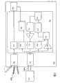
参照图31中的框图描述有源RFID的具体结构。在图31所示的有源RFID 3100中,向信号处理电路3102中的解调电路3105和放大器3106输入由天线电路3101接收的通信信号。通常,通过例如13.56MHz、915MHz等的载波的ASK调制或PSK调制的处理来发送通信信号。图31示出将13.56MHz用于通信信号的情况的实例。在图31中,需要作为基准的时钟信号用于处理信号。这里,将13.56MHz的载波用作时钟信号。放大器3106放大13.56MHz的载波,并将其作为时钟信号提供至逻辑电路3107。然后,在解调电路3105中对于经过ASK调制或PSK调制的通信信号进行解调。将所调制的信号发送到逻辑电路3107进行分析。将逻辑电路3107中分析的信号发送到用于控制存储器电路3109的存储器控制电路3108。将存储器电路3109中存储的数据发送到逻辑电路3110。在逻辑电路3110中编码之后,在放大器3111中对该信号进行放大。通过该信号,调制电路3112调制载波。通过在信号处理电路外部设置的电池3103经过电源电路3104提供用于驱动图31所示的RFID的电力。然后,电源电路3104向放大器3106、解调电路3105、逻辑电路3107、存储器控制电路3108、存储器电路3109、逻辑电路3110、放大器3111、调制电路3112等供应电力。因此,有源RFID运行。A specific structure of the active RFID is described with reference to the block diagram in FIG. 31 . In the
参照图32中的框图描述无源RFID的具体结构。在图32所示的无源RFID 3200中,向信号处理电路3202中的解调电路3205和放大器3206输入由天线电路3201接收的通信信号。通常,通过例如13.56MHz、915MHz等的载波的ASK调制或PSK调制的处理来发送通信信号。图32示出将13.56MHz用于通信信号的情况的实例。在图32中,需要作为基准的时钟信号用于处理信号。这里,将13.56MHz的载波用作时钟信号。放大器3206放大13.56MHz的载波,并将其作为时钟信号提供至逻辑电路3207。然后,在解调电路3205中对于经过ASK调制或PSK调制的通信信号进行解调。将所调制的信号发送到逻辑电路3207进行分析。将逻辑电路3207中分析的信号发送到用于控制存储器电路3209的存储器控制电路3208。将存储器电路3209中存储的数据发送到逻辑电路3210。在逻辑电路3210中编码之后,在放大器3211中对该信号进行放大。通过该信号,调制电路3212调制载波。同时,对于向整流电路3203中输入的通信信号进行整流,从而输入到电源电路3204。电源电路3204向放大器3206、解调电路3205、逻辑电路3207、存储器控制电路3208、存储器电路3209、逻辑电路3210、放大器3211、调制电路3212等供应电力。因此,无源RFID运行。A specific structure of the passive RFID will be described with reference to the block diagram in FIG. 32 . In the
[专利文献1]日本专利申请No.2005-316724[Patent Document 1] Japanese Patent Application No. 2005-316724
[专利文献2]PCT国际申请No.2006-503376的日文翻译[Patent Document 2] Japanese Translation of PCT International Application No. 2006-503376
发明内容Contents of the invention
然而,存在这样的问题,即包括如图31所示设置有驱动电池的有源RFID的半导体器件根据各个信息的发送/接收随时间消耗电力,并且设置用于发送/接收所必须的无线电波的强度,以至于最后不能够产生用于发送/接收各个信息所必须的电力。因此,存在这样的问题,即需要检查驱动电池的剩余容量和改变驱动电池,以继续使用所述包括设置有驱动电池的有源RFID的半导体器件。However, there is a problem that a semiconductor device including an active RFID provided with a drive battery as shown in FIG. Intensity so that in the end the power necessary for sending/receiving each message cannot be generated. Therefore, there is a problem that it is necessary to check the remaining capacity of the driving battery and to change the driving battery in order to continue using the semiconductor device including the active RFID provided with the driving battery.
此外,如图32所示,具有通过外部电磁波(载波)产生驱动力的无源RFID的半导体器件存在这样的问题,即难以保证发送/接收长距离信号以及发送用于发送/接收所必须的电磁波的电力,以及难以实现良好的发送/接收状态。因此,存在这样的问题,仅在提供足够的外部电磁波时(例如,在半导体设置在作为电源提供装置的读取器/写入器的天线附近时),可以使用具有通过外部电磁波(载波)产生驱动力的无源RFID的半导体器件。In addition, as shown in FIG. 32, a semiconductor device having a passive RFID that generates a driving force by an external electromagnetic wave (carrier wave) has such a problem that it is difficult to ensure the transmission/reception of long-distance signals and the transmission of electromagnetic waves necessary for transmission/reception. power, and it is difficult to achieve good transmission/reception status. Therefore, there is such a problem that only when sufficient external electromagnetic waves are supplied (for example, when a semiconductor is provided near the antenna of a reader/writer as a power supply device), the Driving force of passive RFID semiconductor devices.
本发明提供一种包括RFID半导体器件,所述RFID可以在不存在由于作为驱动电源的电池随时间衰退而伴随的电池改变的情况下发送/接收各个信息,以及可向所述RFID提供驱动电力以即使在外部电磁波不足时也能够保持各个信息的良好发送/接收状态。The present invention provides a semiconductor device including an RFID that can transmit/receive various information without battery change due to battery deterioration over time as a driving power source, and that can supply driving power to the RFID to Good transmission/reception status of each information can be maintained even when external electromagnetic waves are insufficient.
为了解决上述问题,在本发明中,将电池(还称为二次电池)设置为提供用于驱动RFID的电力的电源。此外,在本发明中,除了外部发送/接收各种数据的天线之外,还设置用作向电池供应电力的装置的用于对电池无线充电的另一个天线。之后,描述本发明的具体结构。In order to solve the above-mentioned problems, in the present invention, a battery (also referred to as a secondary battery) is provided as a power source that supplies electric power for driving the RFID. Furthermore, in the present invention, in addition to the antenna for externally transmitting/receiving various data, another antenna for wireless charging of the battery serving as means for supplying electric power to the battery is provided. After that, a specific structure of the present invention is described.
本发明的一个模式是一种半导体器件,包括:信号处理电路、可操作地(operationally)连接至所述信号处理电路的第一天线电路和第二天线电路、可操作地连接至所述信号处理电路的电池,其中所述第一天线电路发送/接收用于发送在所述信号处理电路中存储的数据的信号;所述第二天线电路接收用于对所述电池充电的信号;并且由所述第一天线电路接收的信号和由所述第二天线电路接收的信号具有不同的波长。One mode of the present invention is a semiconductor device including: a signal processing circuit, a first antenna circuit and a second antenna circuit operationally connected to the signal processing circuit, a battery of a circuit, wherein the first antenna circuit transmits/receives a signal for transmitting data stored in the signal processing circuit; the second antenna circuit receives a signal for charging the battery; and the The signal received by the first antenna circuit and the signal received by the second antenna circuit have different wavelengths.
本发明的上述模式是这样的半导体器件,其中所述第一天线电路通过读取器/写入器发送用于发送在所述信号处理电路中存储的数据的信号;和所述第二天线电路接收由外部无线电信号对所述电池充电的信号。应注意,作为外部无线电信号,可接收电磁波,只要它们在空气中即可,例如,移动电话交换局的无线电波(800至900MHz频带,1.5GHz频带,1.9至2.1GHz频带等)、从移动电话产生的无线电波、无线电波时钟的无线电波(40kHz等)、和家用交流电源的噪声(60Hz等)。The above mode of the present invention is the semiconductor device, wherein the first antenna circuit transmits a signal for transmitting data stored in the signal processing circuit through a reader/writer; and the second antenna circuit A signal is received to charge the battery by an external radio signal. It should be noted that as external radio signals, electromagnetic waves can be received as long as they are in the air, for example, radio waves (800 to 900MHz band, 1.5GHz band, 1.9 to 2.1GHz band, etc.) Generated radio waves, radio waves of radio-wave clocks (40kHz, etc.), and noise of household AC power (60Hz, etc.).
本发明的一个模式是一种半导体器件,包括:信号处理电路、可操作地连接至所述信号处理电路的第一天线电路和第二天线电路、可操作地连接至所述信号处理电路的电池、和增强(booster)天线,其中所述第一天线电路通过增强天线向/从读取器/写入器发送/接收用于发送在所述信号处理电路中存储的数据的信号;所述第二天线电路接收用于由外部无线电信号对所述电池充电的信号;并且由所述第一天线电路接收的信号和由所述第二天线电路接收的信号具有不同的波长。One mode of the present invention is a semiconductor device including: a signal processing circuit, a first antenna circuit and a second antenna circuit operatively connected to the signal processing circuit, a battery operatively connected to the signal processing circuit , and a booster antenna, wherein the first antenna circuit transmits/receives a signal for transmitting data stored in the signal processing circuit to/from the reader/writer through the booster antenna; Two antenna circuits receive a signal for charging the battery by an external radio signal; and the signal received by the first antenna circuit and the signal received by the second antenna circuit have different wavelengths.
本发明的一个模式是一种半导体器件,包括:信号处理电路;第一天线电路,可操作地连接至所述信号处理电路;多个第二天线电路;电池,可操作地连接至所述信号处理电路;和增强天线,其中所述第一天线电路向/从读取器/写入器发送/接收用于发送在所述信号处理电路中存储的数据的信号;所述第二天线电路通过所述增强天线接收用于由外部无线电信号对所述电池充电的信号;并且由所述第一天线电路接收的信号和由所述第二天线电路接收的信号具有不同的波长。One mode of the present invention is a semiconductor device including: a signal processing circuit; a first antenna circuit operatively connected to the signal processing circuit; a plurality of second antenna circuits; a battery operatively connected to the signal processing circuit; a processing circuit; and a booster antenna, wherein said first antenna circuit transmits/receives a signal for transmitting data stored in said signal processing circuit to/from a reader/writer; said second antenna circuit passes The booster antenna receives a signal for charging the battery by an external radio signal; and the signal received by the first antenna circuit and the signal received by the second antenna circuit have different wavelengths.
本发明的一个模式是一种半导体器件,包括:第一信号处理电路;第二信号处理电路;第一天线电路,可操作地连接至所述第一信号处理电路;第二天线电路,可操作地连接至所述第二信号处理电路;和电池,可操作地连接至所述第一信号处理电路和所述第二信号处理电路,其中所述第一天线电路发送/接收用于发送在所述第一信号处理电路中存储的数据的信号;所述第二天线电路接收用于对所述电池充电的信号;并且由所述第一天线电路接收的信号和由所述第二天线电路接收的信号具有不同的波长。One mode of the present invention is a semiconductor device including: a first signal processing circuit; a second signal processing circuit; a first antenna circuit operatively connected to the first signal processing circuit; a second antenna circuit operable connected to said second signal processing circuit; and a battery operatively connected to said first signal processing circuit and said second signal processing circuit, wherein said first antenna circuit transmits/receives for transmitting the signal of the data stored in the first signal processing circuit; the second antenna circuit receives the signal for charging the battery; and the signal received by the first antenna circuit and the signal received by the second antenna circuit The signals have different wavelengths.
本发明的上述模式是这样的半导体器件,其中所述第一天线电路通过读取器/写入器发送用于发送在所述第一信号处理电路中存储的数据的信号;并且所述第二天线电路接收由外部无线电信号对所述电池充电的信号。应注意,作为外部无线电信号,可接收电磁波,只要它们在空气中即可,例如,移动电话交换局的无线电波(800至900MHz频带,1.5GHz频带,1.9至2.1GHz频带等)、从移动电话产生的无线电波、无线电波时钟的无线电波(40kHz等)、家用交流电源的噪声(60Hz等)。The above mode of the present invention is the semiconductor device wherein the first antenna circuit transmits a signal for transmitting data stored in the first signal processing circuit through a reader/writer; and the second An antenna circuit receives a signal to charge the battery by an external radio signal. It should be noted that as external radio signals, electromagnetic waves can be received as long as they are in the air, for example, radio waves (800 to 900MHz band, 1.5GHz band, 1.9 to 2.1GHz band, etc.) Generated radio waves, radio waves of radio clocks (40kHz, etc.), noise from household AC power (60Hz, etc.).
本发明的一个模式是一种半导体器件,包括:第一信号处理电路;第二信号处理电路;第一天线电路,可操作地连接至所述第一信号处理电路;第二天线电路,可操作地连接至所述第二信号处理电路;电池,可操作地连接至所述第一信号处理电路和所述第二信号处理电路;和增强天线,其中所述第一天线电路通过所述增强天线向/从读取器/写入器发送/接收用于发送在所述第一信号处理电路中存储的数据的信号;所述第二天线电路接收用于由外部无线电信号对所述电池充电的信号;并且由所述第一天线电路接收的信号和由所述第二天线电路接收的信号具有不同的波长。One mode of the present invention is a semiconductor device including: a first signal processing circuit; a second signal processing circuit; a first antenna circuit operatively connected to the first signal processing circuit; a second antenna circuit operable ground connected to the second signal processing circuit; a battery operatively connected to the first signal processing circuit and the second signal processing circuit; and a booster antenna, wherein the first antenna circuit passes through the booster antenna transmits/receives a signal for transmitting data stored in the first signal processing circuit to/from a reader/writer; the second antenna circuit receives a signal for charging the battery by an external radio signal signal; and the signal received by the first antenna circuit and the signal received by the second antenna circuit have different wavelengths.
本发明的一个模式是一种半导体器件,包括:第一信号处理电路;第二信号处理电路;第一天线电路,可操作地连接至所述第一信号处理电路;多个第二天线电路,可操作地连接至所述第二信号处理电路;电池,可操作地连接至所述第一信号处理电路和所述第二信号处理电路;和增强天线,其中所述第一天线电路向/从读取器/写入器发送/接收用于发送在所述第一信号处理电路中存储的数据的信号;所述第二天线电路通过所述增强天线接收用于由外部无线电信号对所述电池充电的信号;并且由所述第一天线电路接收的信号和由所述第二天线电路接收的信号具有不同的波长。One mode of the present invention is a semiconductor device including: a first signal processing circuit; a second signal processing circuit; a first antenna circuit operatively connected to the first signal processing circuit; a plurality of second antenna circuits, operatively connected to said second signal processing circuit; a battery operatively connected to said first signal processing circuit and said second signal processing circuit; and a booster antenna, wherein said first antenna circuit sends to/from a reader/writer transmits/receives a signal for transmitting data stored in said first signal processing circuit; said second antenna circuit receives a the charging signal; and the signal received by the first antenna circuit and the signal received by the second antenna circuit have different wavelengths.
本发明的电池可向所述第一信号处理电路中包括的电源电路供应电力。The battery of the present invention can supply electric power to a power supply circuit included in the first signal processing circuit.
此外,本发明的所述第一天线电路和所述多个第二天线电路中的任一个可通过电磁感应方法接收信号。Also, any one of the first antenna circuit and the plurality of second antenna circuits of the present invention may receive a signal by an electromagnetic induction method.
作为本发明的电池,可使用锂电池、镍氢电池、镍镉电池、有机基电池、或电容器。As the battery of the present invention, a lithium battery, a nickel-hydrogen battery, a nickel-cadmium battery, an organic-based battery, or a capacitor can be used.
在本发明中,“连接”表示“电连接”和“直接连接”。因此,在本发明所公开的结构中,除了预定连接之外,可设置能够建立电连接的其他元件(例如,开关、晶体管、电容器、电感器、电阻器、二极管等)。可选择地,可以在不插入其他元件的情况下直接连接。应注意,在没有插入能实现电连接的其他元件对元件进行连接,并且不是电连接而是直接连接时,称为“直接连接”。应注意,“电连接”也意味着“直接连接”。In the present invention, "connected" means "electrically connected" and "directly connected". Therefore, in the structures disclosed herein, in addition to predetermined connections, other elements capable of establishing electrical connections (eg, switches, transistors, capacitors, inductors, resistors, diodes, etc.) may be provided. Alternatively, a direct connection can be made without intervening other components. It should be noted that when elements are connected without intervening other elements capable of realizing electrical connection, and are not electrically connected but directly connected, it is called "direct connection". It should be noted that "electrically connected" also means "directly connected".
应注意,可对于本发明的晶体管采用各种模式的晶体管。因此,适用于本发明的晶体管类型没有限制。因此,以下晶体管适用于本发明,包括:使用按非晶硅和多晶硅分类的非单晶半导体膜的薄膜晶体管(TFT);使用半导体衬底或SOI衬底形成的晶体管;MOS晶体管;结式晶体管;双极晶体管;使用例如ZnO或a-InGaZnO的化合物半导体的晶体管;使用有机半导体或碳纳米管的晶体管;和其他晶体管。应注意,非单晶半导体膜可包含氢或卤素。在上面设置有晶体管的衬底不限于特定类型,并且可使用各种类型衬底。因此,晶体管可设置在例如单晶衬底、SOI衬底、玻璃衬底、石英衬底、塑料衬底、纸衬底、玻璃纸(cellophane)衬底、石衬底等上。此外,可将一定衬底上形成的晶体管转移到其他衬底。It should be noted that various modes of transistors can be employed for the transistors of the present invention. Therefore, the type of transistors suitable for use in the present invention is not limited. Therefore, the following transistors are applicable to the present invention, including: a thin film transistor (TFT) using a non-single crystal semiconductor film classified by amorphous silicon and polycrystalline silicon; a transistor formed using a semiconductor substrate or an SOI substrate; a MOS transistor; a junction transistor ; bipolar transistors; transistors using compound semiconductors such as ZnO or a-InGaZnO; transistors using organic semiconductors or carbon nanotubes; and other transistors. It should be noted that the non-single crystal semiconductor film may contain hydrogen or halogen. A substrate on which transistors are provided is not limited to a specific type, and various types of substrates may be used. Accordingly, a transistor can be provided on, for example, a single crystal substrate, an SOI substrate, a glass substrate, a quartz substrate, a plastic substrate, a paper substrate, a cellophane substrate, a stone substrate, or the like. In addition, transistors formed on one substrate can be transferred to other substrates.
应注意,应用于本发明的半导体器件的晶体管可具有例如栅极数目为2或更多的多栅极结构。通过多栅极结构,由于即使在漏极-源极电压在运行时在饱和区中改变时漏极-源极电流也没有大的改变,所以可通过提高晶体管的压力阻抗来减少关断电流和提高可靠性,并获得扁平特征。此外,栅电极可设置在沟道上方和下方。因此,沟道区域增加,从而电流值增加,或者,由于耗尽层容易形成,所以S值可提高。此外,栅电极可设置在沟道上方或下方。可采用前向交错结构或逆向交错结构。可将沟道区域分成多个区域,这些区域或并联或串联连接。此外,源电极或漏电极可与沟道(或其一部分)重叠,因此防止电荷在沟道的一部分中聚集以及防止不稳定操作。此外,可设置LDD区。通过设置LDD区,由于即使在漏极-源极电压在运行时在饱和区中改变时漏极-源极电流也没有大的改变,所以可通过提高晶体管的压力阻抗来减少关断电流和提高可靠性,并获得扁平特征。It should be noted that the transistor applied to the semiconductor device of the present invention may have, for example, a multi-gate structure in which the number of gates is 2 or more. With the multi-gate structure, since the drain-source current does not change greatly even when the drain-source voltage changes in the saturation region during operation, it is possible to reduce the off-current and Improve reliability and get flat features. In addition, a gate electrode may be disposed above and below the channel. Therefore, the channel region increases, so that the current value increases, or, since the depletion layer is easily formed, the S value can be increased. In addition, the gate electrode may be disposed above or below the channel. A forward staggered structure or a reverse staggered structure can be used. The channel region can be divided into multiple regions, which are connected either in parallel or in series. In addition, a source electrode or a drain electrode may overlap the channel (or a portion thereof), thus preventing charges from accumulating in a portion of the channel and preventing unstable operation. In addition, an LDD area may be provided. By setting the LDD region, since the drain-source current does not change greatly even when the drain-source voltage changes in the saturation region during operation, it is possible to reduce the off-state current and improve reliability, and obtain flat features.
应注意,可将各种类型的晶体管用作应用于本发明的半导体器件的并且在上述各种衬底上形成的晶体管。因此,所有电路可形成在玻璃衬底、塑料衬底、单晶硅衬底、SOI衬底或任意衬底上。当所有电路形成在衬底上时,可通过减少组件的数目来减少成本,以及通过减少与组件连接的数目来提高可靠性。可选择地,可在一定衬底上形成一部分电路,在另一个衬底上形成另一部分电路。即,不需要所有电路形成在同一个衬底上。例如,一部分电路可使用晶体管形成在玻璃衬底上,另一部分电路可形成在IC芯片中的单晶硅衬底上,其中所述IC芯片可通过COG(玻璃上芯片)设置在玻璃衬底上。可选择地,IC芯片可使用TAB(带自动接合)连接至玻璃衬底或印刷衬底。这样,在一部分电路形成在同一个衬底上时,可通过减少组件的数目来减少成本,以及可通过减少与组件连接的数目来提高可靠性。此外,消耗更多电力的具有高驱动电压或高驱动频率的部分没有形成在同一个衬底上,因此可防止电力消耗的增加。It should be noted that various types of transistors can be used as the transistors applied to the semiconductor device of the present invention and formed on the above-described various substrates. Therefore, all circuits can be formed on glass substrates, plastic substrates, single crystal silicon substrates, SOI substrates, or arbitrary substrates. When all circuits are formed on a substrate, cost can be reduced by reducing the number of components, and reliability can be improved by reducing the number of connections to components. Alternatively, a portion of circuitry may be formed on a certain substrate and another portion of circuitry may be formed on another substrate. That is, all circuits need not be formed on the same substrate. For example, a part of the circuit can be formed on a glass substrate using transistors, and another part of the circuit can be formed on a single crystal silicon substrate in an IC chip that can be provided on the glass substrate by COG (Chip On Glass) . Alternatively, the IC chip can be attached to a glass substrate or a printed substrate using TAB (Tape Automated Bonding). Thus, when a part of circuits is formed on the same substrate, cost can be reduced by reducing the number of components, and reliability can be improved by reducing the number of connections to components. In addition, a portion having a high driving voltage or a high driving frequency that consumes more power is not formed on the same substrate, so an increase in power consumption can be prevented.
应注意,本说明书的半导体器件对应于可通过利用半导体特性工作的一般器件。It should be noted that the semiconductor device of this specification corresponds to a general device that can operate by utilizing semiconductor characteristics.
本发明的半导体器件具有电池,因此它可防止用于发送/接收各个信息的电力根据电池随时间的衰退而变低。此外,本发明的半导体器件具有向电池无线地供应电力的天线。因此,半导体器件可以不直接与充电器连接的情况下通过将外部电磁波的电力用作驱动半导体器件的电源对电池充电。因此,能够在不需要检查电池容量或改变电池(这是在有源RFID的情况下所必须)的情况下继续使用半导体器件。此外,将驱动半导体器件的电力始终保存在电池中,从而可获得足够运行半导体器件的电力,以及可扩展与读取器/写入器的通信距离。The semiconductor device of the present invention has a battery, so it can prevent the electric power for transmitting/receiving each information from becoming low according to deterioration of the battery over time. Furthermore, the semiconductor device of the present invention has an antenna for wirelessly supplying electric power to a battery. Therefore, the semiconductor device can charge the battery by using the power of external electromagnetic waves as a power source for driving the semiconductor device without being directly connected to the charger. Therefore, it is possible to continue using the semiconductor device without checking the battery capacity or changing the battery, which is necessary in the case of active RFID. In addition, the power to drive the semiconductor device is always kept in the battery, making it possible to obtain enough power to operate the semiconductor device and to extend the communication distance with the reader/writer.
附图说明Description of drawings
图1是示出本发明的半导体器件的结构实例的示图。FIG. 1 is a diagram showing a structural example of a semiconductor device of the present invention.
图2是示出本发明的半导体器件的结构实例的示图。FIG. 2 is a diagram showing a structural example of a semiconductor device of the present invention.
图3A至图3E是分别示出本发明的半导体器件中包括的天线形状的示图。3A to 3E are diagrams respectively showing shapes of antennas included in the semiconductor device of the present invention.
图4A和图4B是分别示出本发明的半导体器件的结构实例的示图。4A and 4B are diagrams each showing a structural example of a semiconductor device of the present invention.
图5是示出本发明的半导体器件的结构实例的示图。FIG. 5 is a diagram showing a structural example of a semiconductor device of the present invention.
图6是示出本发明的半导体器件的结构实例的示图。FIG. 6 is a diagram showing a structural example of a semiconductor device of the present invention.
图7是示出本发明的半导体器件的结构实例的示图。FIG. 7 is a diagram showing a structural example of a semiconductor device of the present invention.
图8是示出本发明的半导体器件的结构实例的示图。FIG. 8 is a diagram showing a structural example of a semiconductor device of the present invention.
图9A至图9C是分别示出本发明的半导体器件的结构实例的示图。9A to 9C are diagrams each showing a structural example of the semiconductor device of the present invention.
图10A和图10B是分别示出本发明的半导体器件的结构实例的示图。10A and 10B are diagrams each showing a structural example of a semiconductor device of the present invention.
图11A至图11F是分别示出本发明的半导体器件的结构实例的示图。11A to 11F are diagrams each showing a structural example of the semiconductor device of the present invention.
图12是示出本发明的半导体器件的结构实例的示图。FIG. 12 is a diagram showing a structural example of a semiconductor device of the present invention.
图13是示出本发明的半导体器件的结构实例的示图。FIG. 13 is a diagram showing a structural example of a semiconductor device of the present invention.
图14是示出本发明的半导体器件的结构实例的示图。FIG. 14 is a diagram showing a structural example of a semiconductor device of the present invention.
图15是示出本发明的半导体器件的结构实例的示图。FIG. 15 is a diagram showing a structural example of a semiconductor device of the present invention.
图16是示出本发明的半导体器件的结构实例的示图。FIG. 16 is a diagram showing a structural example of a semiconductor device of the present invention.
图17是示出本发明的半导体器件的结构实例的示图。FIG. 17 is a diagram showing a structural example of a semiconductor device of the present invention.
图18是示出本发明的半导体器件的结构实例的示图。FIG. 18 is a diagram showing a structural example of a semiconductor device of the present invention.
图19A至图19D是分别示出本发明的半导体器件的制造方法的结构实例的示图。19A to 19D are diagrams each showing a structural example of a method of manufacturing a semiconductor device of the present invention.
图20A至图20C是分别示出本发明的半导体器件的制造方法的结构实例的示图。20A to 20C are diagrams each showing a structural example of a method of manufacturing a semiconductor device of the present invention.
图21A和图21B是分别示出本发明的半导体器件的制造方法的结构实例的示图。21A and 21B are diagrams each showing a structural example of a method of manufacturing a semiconductor device of the present invention.
图22A和图22B是分别示出本发明的半导体器件的制造方法的结构实例的示图。22A and 22B are diagrams each showing a structural example of a method of manufacturing a semiconductor device of the present invention.
图23A和图23B是分别示出本发明的半导体器件的制造方法的结构实例的示图。23A and 23B are diagrams each showing a structural example of a method of manufacturing a semiconductor device of the present invention.
图24A至图24D是分别示出本发明的半导体器件的制造方法的结构实例的示图。24A to 24D are diagrams each showing a structural example of a method of manufacturing a semiconductor device of the present invention.
图25A和图25B是分别示出本发明的半导体器件的制造方法的结构实例的示图。25A and 25B are diagrams each showing a structural example of a method of manufacturing a semiconductor device of the present invention.
图26是示出本发明的半导体器件的制造方法的结构实例的示图。FIG. 26 is a diagram showing a structural example of a method of manufacturing a semiconductor device of the present invention.
图27是示出本发明的半导体器件的制造方法的结构实例的示图。FIG. 27 is a diagram showing a structural example of a method of manufacturing a semiconductor device of the present invention.
图28A和图28B是分别示出本发明的半导体器件的制造方法的结构实例的示图。28A and 28B are diagrams each showing a structural example of a method of manufacturing a semiconductor device of the present invention.
图29A和图29B是分别示出本发明的半导体器件的制造方法的结构实例的示图。29A and 29B are diagrams each showing a structural example of a method of manufacturing a semiconductor device of the present invention.
图30A至图30E是分别示出本发明的半导体器件的应用模式的实例的示图。30A to 30E are diagrams each showing an example of an application mode of the semiconductor device of the present invention.
图31是示出传统结构的示图。Fig. 31 is a diagram showing a conventional structure.
图32是示出传统结构的示图。Fig. 32 is a diagram showing a conventional structure.
图33A至图33D是分别示出本发明的半导体器件的应用模式的实例的示图。33A to 33D are diagrams each showing an example of an application mode of the semiconductor device of the present invention.
图34A和图34B是分别示出本发明的半导体器件的特性的示图。34A and 34B are diagrams respectively showing characteristics of the semiconductor device of the present invention.
图35是示出本发明的半导体器件的结构实例的示图。FIG. 35 is a diagram showing a structural example of a semiconductor device of the present invention.
图36是示出本发明的半导体器件的结构实例的示图。FIG. 36 is a diagram showing a structural example of a semiconductor device of the present invention.
图37是示出本发明的半导体器件的操作方法的实例的示图。FIG. 37 is a diagram showing an example of an operating method of the semiconductor device of the present invention.
图38是示出本发明的半导体器件的操作方法的实例的示图。FIG. 38 is a diagram showing an example of an operating method of the semiconductor device of the present invention.
图39是示出本发明的半导体器件的操作方法的实例的示图。FIG. 39 is a diagram showing an example of an operating method of the semiconductor device of the present invention.
图40是示出本发明的半导体器件的操作方法的实例的示图。FIG. 40 is a diagram showing an example of an operating method of the semiconductor device of the present invention.
图41是示出本发明的半导体器件的结构实例的示图。FIG. 41 is a diagram showing a structural example of a semiconductor device of the present invention.
具体实施方式Detailed ways
尽管参照附图通过实施方式和实施例完整描述本发明,但是可以理解,对于本领域普通技术人员来说,各种变化和修改是清楚的。因此,除非这种变化和修改脱离本发明的实质和范围,否则他们应理解为包括在本发明中。应注意,在本发明结构的所有附图中,通过相同的标号表示共同的部分,如以下所述。Although the present invention has been fully described by way of embodiments and examples with reference to the accompanying drawings, it is to be understood that various changes and modifications will be apparent to those skilled in the art. Therefore, unless such changes and modifications depart from the spirit and scope of the present invention, they should be construed as being included therein. It should be noted that in all drawings of the structure of the present invention, common parts are denoted by the same reference numerals, as described below.
(实施方式1)(Embodiment 1)
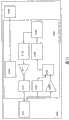
参照图1和2所示的框图描述本发明的半导体器件的结构实例。应注意,在本实施方式中,描述了将半导体器件用作RFID标签(以下,简单称为“RFID”)的情况。A structural example of the semiconductor device of the present invention will be described with reference to the block diagrams shown in FIGS. 1 and 2 . It should be noted that in this embodiment mode, a case where a semiconductor device is used as an RFID tag (hereinafter, simply referred to as "RFID") is described.
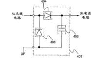
图1中所示的半导体器件(以下,称为“RFID 100”)包括:第一天线电路101、第二天线电路102、信号处理电路103和电池104。信号处理电路103包括:第一整流电路105、电源电路106、第二整流电路107、解调电路108、放大器109、逻辑电路110、存储器控制电路111、存储器电路112、逻辑电路113、放大器114和调制电路115。The semiconductor device shown in FIG. 1 (hereinafter, referred to as "
图2示出第一天线电路101接收从读取器/写入器201产生的无线电波202a(或向读取器/写入器201发送无线电波)以及第二天线电路102接收外部无线电波202b的情况。在图2中,通过第一整流电路105向电源电路106输入由第一天线电路101接收的无线电波202a,并且此时,通过解调电路108等提取在无线电波202a中包含的数据。此外,通过第二整流电路107向电池104输入由第二天线电路102接收的无线电波202b。2 shows that the
在本实施方式中描述的RFID 100的情况下,向电池104输入由第二天线电路102接收的外部无线电波202b,从而对电池104充电。通过电源电路106向信号处理电路103中设置的电路提供在电池104中充电的电力。换句话说,以无线方式对电池104充电。此外,通过电源电路106向信号处理电路103提供由第一天线电路101接收的并且通过第一整流电路105输入的无线电波202a,作为用于驱动RFID100的电力。In the case of the
应注意,在本实施方式中描述的RFID 100使用外部无线电波202b(以下还称为“无线电信号”)作为由第二天线电路102接收的无线电波,以对电池104充电。对于无线电信号,可使用移动电话交换局的无线电波(800至900MHz频带,1.5GHz频带,1.9至2.1GHz频带等)、从移动电话产生的无线电波、无线电波时钟的无线电波(40kHz等)、家用交流电源的噪声(60Hz等)、从另一个读取器/写入器随机产生的无线电波(不与RFID 100直接通信的读取器/写入器)等。此外,设置包括不同长度和不同天线的多个天线电路作为第二天线电路102,从而可以在对电池104充电时使用包括不同波长的多个无线电信号。It should be noted that the
由于通过接收上述无线电波的无线方式对电池充电,所以不需要额外的充电器对电池充电;因此,不必改变电池。因此,可以以更低成本设置RFID。将第二天线电路102的天线设置为可容易接收这些无线电波信号的这种长度和形状。在接收包括不同波长的多个无线电信号的情况下,优选地,设置具有不同长度和不同形状的天线的多个天线电路。Since the battery is charged wirelessly by receiving the above-mentioned radio waves, an additional charger is not required to charge the battery; therefore, it is not necessary to change the battery. Therefore, RFID can be installed at a lower cost. The antenna of the
应注意,第一天线电路101和第二天线电路102均可由图4A所示的天线401和谐振电容器402构成,在一些情况下,将天线401和谐振电容器402的组合称为天线电路403。第一整流电路105和第二整流电路107仅需要将第一天线电路101和第二天线电路102接收的电磁波所感应的交流信号转行成直流信号。例如,如图4B所示,整流电路407可由二极管404、二极管405和平滑电容器406构成。It should be noted that both the
第一天线电路101的天线的形状没有具体限制:可使用电磁耦合方法、电磁感应方法、微波方法等作为应用于RFID 100的第一天线电路101的信号传输方法。可根据用途适当选择传输方法,可依据传输方法设置具有最佳长度和形状的天线。The shape of the antenna of the
在采用例如电磁耦合方法或电磁感应方法(例如,13.56MHz频带)作为传输方法的情况下,使用通过变化磁场密度所产生的电磁感应。因此,用作天线的导电膜可形成为环形(例如,回路天线)或螺旋形(例如,螺旋天线)。In the case of employing, for example, an electromagnetic coupling method or an electromagnetic induction method (eg, 13.56 MHz band) as a transmission method, electromagnetic induction generated by varying the magnetic field density is used. Therefore, a conductive film serving as an antenna may be formed in a ring shape (for example, a loop antenna) or a spiral shape (for example, a helical antenna).
在采用例如微波方法(例如,UHF频带(860至960MHz频带)或2.45GHz频带)作为传输方法的情况下,可考虑用于信号传输的电磁波的波长来适当设置例如用作天线的导电膜长度的形状。例如,用作天线的导电膜可形成为线性形状(例如,偶极天线)、平面形状(例如,平板天线)等。用作天线的导电膜的形状不限于线性形状,考虑到电磁波的波长,用作天线的导电膜可设置成曲线形、蜿蜒形、或其组合。In the case of employing, for example, a microwave method (for example, UHF band (860 to 960 MHz band) or 2.45 GHz band) as the transmission method, the length of the conductive film used, for example, as an antenna can be appropriately set in consideration of the wavelength of the electromagnetic wave used for signal transmission. shape. For example, a conductive film used as an antenna may be formed in a linear shape (eg, a dipole antenna), a planar shape (eg, a planar antenna), or the like. The shape of the conductive film used as an antenna is not limited to a linear shape, and the conductive film used as an antenna may be arranged in a curved shape, a meander shape, or a combination thereof in consideration of the wavelength of electromagnetic waves.
图3A至3E示出在采用微波方法的情况下对于第一天线电路101或第二天线电路102设置的天线形状的实例。例如,如图3A所示,天线303可被设置为在设置有信号处理电路的芯片302的外部延伸。如图3B所示,很薄的天线303可被设置在设置有信号处理电路的芯片302的上方。如图3C所示,天线303可具有相对于设置有信号处理电路的芯片302的用于接收高频电磁波的形状。如图3D所示,天线303可具有相对于设置有信号处理电路的芯片302的180度全方向形状(能够在任意方向接收信号)。如图3E所示,天线303可具有相对于设置有信号处理电路的芯片302延伸的长棒的形状。当对于第一天线电路101和第二天线电路102采用微波方法时,可组合使用包括这些形状的天线。3A to 3E show examples of antenna shapes provided for the
此外,在图3A至3E中,对于设置有信号处理电路的芯片和天线的连接没有具体限制。例如,天线303和芯片302可通过引线接合连接或凸块连接的方式连接。可选择地,芯片可通过作为电极的一部分芯片附接于天线303。在该方法中,可使用ACF(各向异性导电膜)将芯片302附接于天线303。对于天线所需的适当长度根据接收信号的频率改变。因此,长度是波长的约数。例如,在频率为2.45GHz的情况下,天线的长度可以是大约60mm(1/2波长)和大约30mm(1/4波长)。Furthermore, in FIGS. 3A to 3E , there is no specific limitation on the connection of the chip provided with the signal processing circuit and the antenna. For example, the
应注意,图1和2中的电源电路106向每一个电路提供用于驱动RFID 100的电力。具体地,它控制通过由第一天线电路101接收并且在第一整流电路105中整流所获得的电力以具有确定值,并且提供用于运行信号处理电路103的每一个电路所必须的电力。此外,它控制在电池104中充电的电力以具有确定值,并且提供用于运行信号处理电路103的每一个电路所必须的电力。即使当没有通过RFID 100的第一天线电路101获得足够电力时,也可以通过电池104中充电的电力提供用于运行信号处理电路103的每一个电路所必须的电力。It should be noted that the
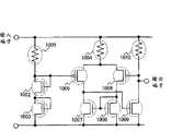
参照图6描述图1和2中的电源电路的实例。电源电路包括基准电压电路和缓冲放大器。基准电压电路包括:电阻器1001和二极管接法晶体管1002和1003,并且产生与晶体管的两个Vg对应的基准电压。缓冲放大器包括:由晶体管1005和1006构成的微分电路、由晶体管1007和1008构成的电流反射镜电路、由电流源电阻器1004、晶体管1009和电阻器1010构成的共源极放大器。An example of the power supply circuit in FIGS. 1 and 2 is described with reference to FIG. 6 . The power supply circuit includes a reference voltage circuit and a buffer amplifier. The reference voltage circuit includes: a
在图6中所示的电源电路中,当从输出端子流过的电流的量较大时,流过晶体管1009的电流的量减小;当从输出端子流过的电流的量较小时,流过晶体管1009的电流的量增加;流过晶体管1010的电流几乎恒定。输出端子的电位与基准电压电路具有大约相同的值。尽管这里示出包括基准电压电路和缓冲放大器的电源电路,但是在本发明中使用的电源电路不限于图6所示的部分,它还可以是包括其他形式的电路。In the power supply circuit shown in FIG. 6, when the amount of current flowing from the output terminal is large, the amount of current flowing through the
应注意,在本说明书中,电池指的是可通过充电恢复其连续运行时间的电池。换句话说,电池指的是具有根据电力消耗而减少的运行时间并且可通过补充因消耗而减少的电力来延伸运行时间的电池。具体地,可将以下的电池作为电池,包括:锂离子电池、锂二次电池、镍氢电池、镍镉电池、有机基电池、铅酸电池、空气二次电池、镍锌电池、银锌电池等。电池不限于这些,并且可使用高容量电容器。具体地,锂离子电池和锂二次电池具有较高的充电容量和放电容量;因此,将其用作为本实施方式的半导体器件而设置的电池,因此可实现半导体器件的小型化。It should be noted that in this specification, a battery refers to a battery whose continuous operating time can be restored by charging. In other words, a battery refers to a battery that has a reduced operating time according to power consumption and can extend the running time by supplementing the reduced power due to consumption. Specifically, the following batteries can be used as batteries, including: lithium-ion batteries, lithium secondary batteries, nickel-metal hydride batteries, nickel-cadmium batteries, organic-based batteries, lead-acid batteries, air secondary batteries, nickel-zinc batteries, silver-zinc batteries wait. The battery is not limited to these, and high-capacity capacitors may be used. Specifically, a lithium ion battery and a lithium secondary battery have high charge capacity and discharge capacity; therefore, they are used as the battery provided as the semiconductor device of the present embodiment, and thus miniaturization of the semiconductor device can be achieved.
接下来,描述图1和2中所示通过读取器/写入器201向RFID 100写入数据的操作。通过整流电路105将第一天线电路101接收的信号进行半波整流,然后对其平滑化。向电源电路106输入通过第一整流电路105半波整流和平滑化的电压。电源电路向放大器109、逻辑电路110、存储器控制电路111、存储器电路112、逻辑电路113、放大器114和调制电路115提供稳定的电压。Next, the operation of writing data to the
通过放大器109向逻辑电路110输入由第一天线电路101接收的信号作为时钟信号。此外,在解调电路108中对于从第一天线电路101输入的信号进行解调,然后将其作为数据输入到逻辑电路110。The signal received by the
在逻辑电路110中,解码所输入的数据。读取器/写入器201通过转换镜码、NRZ-L码等对数据编码以进行发送,然后逻辑电路110对数据解码。然后,在将所解码的数据发送到存储器控制电路111时,将数据写入到存储器电路112。存储器电路112需要是即使在电源切断时也能够保存数据的非易失性存储器电路,因此可使用掩模ROM等。In the
为了读取在图1和2所示的RFID 100中的存储器电路112中存储的数据,读取器/写入器201如下运行。通过第一整流电路105对第一天线电路101接收的信号进行半波整流,然后对其平滑化。向电源电路106输入通过第一整流电路105半波整流和平滑化的电压。电源电路向放大器109、逻辑电路110、存储器控制电路111、存储器电路112、逻辑电路113、放大器114和调制电路115提供稳定的电压。In order to read data stored in the
向逻辑电路110输入由第一天线电路101接收的交流信号,并进行逻辑运算。然后,将来自逻辑电路110的信号用于控制存储器控制电路111,并调用在存储器电路112中存储的数据。在逻辑电路113中处理从存储器电路112调用的数据并然后在放大器114中对其放大之后,运行调制电路115。根据ISO14443、ISO15693、ISO18000等规定的方法处理数据。可使用其他标准规定的方法,只要保证与读取器/写入器一致即可。The AC signal received by the
当调制电路115运行时,第一天线电路101的阻抗改变。因此,在第一天线电路101中反射的读取器/写入器201的信号变化。由读取器/写入器读取该变化,从而能够获知RFID 100的存储器电路112中存储的数据。这种调制方法称为负载调制方法。When the
应注意,对于信号处理电路103而设置的晶体管可采用各种模式的晶体管。因此,适用于本发明的晶体管的类型没有限制。因此,以下晶体管适用于本发明,包括:使用按非晶硅和多晶硅分类的非单晶半导体膜的薄膜晶体管(TFT);使用半导体衬底或SOI衬底形成的晶体管;MOS晶体管;结式晶体管;双极晶体管;使用例如ZnO或a-InGaZnO的化合物半导体的晶体管;使用有机半导体或碳纳米管的晶体管;以及其它晶体管。应注意,非单晶半导体膜可包含氢或卤素。在上面设置有信号处理电路1102的衬底不限于特定类型,并且可使用各种类型衬底。因此,信号处理电路1102可设置在例如单晶衬底、SOI衬底、玻璃衬底、石英衬底、塑料衬底、纸衬底、玻璃纸衬底、石衬底等上。此外,可将一定衬底上形成的信号处理电路1102转移到其他衬底。It should be noted that transistors provided for the
接下来,描述由外部无线电信号向图1和2中所示的RFID 100充电的操作。通过第二整流电路107对第二天线电路102接收的外部无线电信号进行半波整流,然后对其平滑化。将通过第二整流电路107半波整流和平滑化的电压临时存储在电池104中。将电池104中保存的电力用作向电源电路106提供的电力。应注意,可采用这样的结构,即,在可接收从第一天线电路提供的信号但是向读取器/写入器发送的信号的电力不足时,用于确定是否从电池提供的电力的电路。Next, the operation of charging the
之后,描述在本实施方式的RFID的结构实例。应注意,这里描述在第一天线电路101中设置的天线是线圈形状,以及设置具有不同长度和不同形状的天线的多个天线电路作为第二天线电路102的情况。Next, a structural example of the RFID in the present embodiment is described. It should be noted that the case where the antenna provided in the
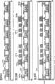
将本实施方式的RFID 100按功能和大小分成第一天线电路、第二天线电路、信号处理电路和电池,并且它们在衬底上堆叠或平行排列。此外,信号处理电路可分成伴随第一天线电路的电路以及伴随第二天线电路的电路。在以下的说明中,伴随第一天线电路的电路以及伴随第二天线电路的电路分别称为第一信号处理电路和第二信号处理电路。应注意,第一信号处理电路至少包括:图1中的信号处理电路103的第一逻辑电路105、电源电路106、解调电路108、放大器109、逻辑电路110、存储器控制电路111、存储器电路112、逻辑电路113、放大器114和调制电路115。另一方面,第二信号处理电路至少包括图1中的信号处理电路103的第二整流电路107。The
图7中所示的RFID包括:第一天线电路704、多个第二天线电路705a和705b、含有第一信号处理电路和第二信号处理电路的芯片702、和电池703。应注意,第一天线电路704可操作地连接至第一信号处理电路,第二天线电路705a和705b可操作地连接至第二信号处理电路。The RFID shown in FIG. 7 includes a
通过在芯片702中形成的第一信号处理电路中的第一整流器电路向电源电路输入由第一天线电路704接收的无线电波,以在解调电路等提取无线电波中包括的信号的同时产生电力。电池703可操作地连接至芯片702中形成的第二信号处理电路,并且通过第二信号处理电路中的整流器电路向电池703输入由多个第二天线电路705a和705b接收的无线电波。Radio waves received by the
这里,示出由第一天线电路704接收从读取器/写入器706发送的无线电波以及由第二天线电路705a和705b接收外部无线电信号707的情况。换句话说,RFID通过第一天线电路704向/从读取器/写入器706发送/接收数据,以及通过第二天线电路705a和705b对电池703充电。Here, a case is shown in which radio waves transmitted from the reader/
此外,电池703也可操作地电连接至在芯片702中设置的第一信号处理电路,并且适当地从电池703向第一信号处理电路中的电源电路供应电力。关于在电池703和第一信号处理电路或第二信号处理电路的连接没有限制。例如,电池703可通过引线接合连接或凸块连接的方式可操作地连接至第一信号处理电路或第二信号处理电路。可选择地,第一信号处理电路或第二信号处理电路可通过用作电极的一部分第一信号处理电路或第二信号处理电路(在这种情况下,通过使用各向异性导电膜等)附接于具有电池703的连接端子。In addition, the
参照图5描述图7中的读取器/写入器706的实例。图5中的读取器/写入器706包括:接收部分501、发送部分502、控制部分503、接口部分504和天线电路505。控制部分503通过利用接口部分504控制更高级设备506的方式在数据处理命令(order)和数据处理结果方面控制发送部分502。发送部分502控制向RFID 100发送的数据处理命令,然后从天线电路505将其作为电磁波输出。接收部分501解调由天线电路505接收的信号,然后将其作为数据处理结果输出至控制部分503。An example of the reader/
在本实施方式中,图5中所示的读取器/写入器706的天线电路505连接至接收部分501和发送部分502,并且具有形成LC并联谐振电路的天线507和谐振电容器508。天线电路505通过从RFID 100输出的信号接收对于天线电路505感应的电动势作为电信号。此外,天线电路505提供感应电流,以向RFID 100发送信号。In the present embodiment, an
用于对电池703充电的第二天线电路705a和705b的长度和形状不限于图7所示的部件。这里,示出设置不同长度的线性天线(偶极天线)作为第二天线电路705a和705b的天线的实例。可选择地,例如,可使用偶极天线和线圈天线的组合或偶极天线和平板天线的组合。因此,可设置具有不同长度和形状的多个天线,作为用于对电池703充电的天线,从而可接收各种波长的无线电信号。因此,可提高充电效率。具体地,在设置具有不同形状的天线(例如平板天线和偶极天线)的组合(例如,在平板天线的周围设置折叠偶极天线)时,能够有效利用有限的空间。不言而喻,尽管示出在本实施方式中描述的RFID设置有多个第二天线电路705a和705b的情况,但是本发明不限于此。相反,可采用设置一个天线电路的结构或设置三个或更多天线电路的结构。The length and shape of the
此外,用于向/从读取器/写入器706发送/接收信号的第一天线电路704不限于具有图7所示的结构。如上所述,可根据要采用的传输方法使用包括不同长度和形状的天线。Furthermore, the
例如,对于在第一天线电路704和读取器/写入器706之间发送/接收的信号频率,可给出均由ISO标准规定的125KHz、13.56MHz、915MHz、2.45GHz等。不言而喻,在第一天线电路704和读取器/写入器706之间发送/接收的信号频率不限于此,可使用以下任意一个:300GHz至3THz的亚毫米波;30GHz至300GHz的毫米波;3GHz至30GHz的微波;300MHz至3GHz的超短波;30MHz至300MHz的甚短波;3MHz至30MHz的短波;300KHz至3MHz的中波;30KHz至300KHz的长波,和3KHz至30KHz的超长波。此外,在第一天线电路704和读取器/写入器706之间发送/接收的信号是通过调制载波获得的信号。可通过模拟调制或数字调制对载波进行调制,以及可采用幅度调制、相位调制、频率调制、和扩展频谱调制中的任一个。期望地,采用幅度调制或频率调制。For example, for the signal frequency transmitted/received between the
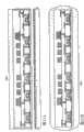
应注意,尽管图7中示出在衬底701上设置第一天线电路704、多个第二天线电路705a和705b、包括第一信号处理电路和第二信号处理电路的芯片702、和电池703的实例,但是在本实施方式中所述的RFID不限于具有图7中所示的结构。It should be noted that although it is shown in FIG. 7 that a
例如,如图8所示,可采用将设置有芯片702a和第一天线电路704的衬底701a和设置有芯片702b、多个第二天线电路705a和705b、和电池703的衬底701b彼此重叠的结构。芯片702a设置有第一信号处理电路,芯片702b设置有第二信号处理电路。For example, as shown in FIG. 8, a
在图8中,通过在芯片702a中设置的第一信号处理电路中的第一整流电路向电源电路输入由第一天线电路704接收的无线电信号,以在解调电路等提取无线电波中包括的信号的同时产生电力。通过在芯片702b中设置的第二信号处理电路中的第二整流电路向电池703输入由第二天线电路705a和705b接收的无线电波。In FIG. 8, the radio signal received by the
第一天线电路704可操作地连接至在芯片702a中设置的第一信号处理电路。第二天线电路705a和705b可操作地连接至在芯片702b中设置的第二信号处理电路。设置电池703,以可操作地电连接至在芯片702a中设置的第一信号处理电路和在芯片702b中设置的第二信号处理电路。The
关于电池703和第一信号处理电路或第二信号处理电路的连接没有限制。例如,电池703可通过引线接合连接或凸块连接的方式可操作地连接至第一信号处理电路或第二信号处理电路。可选择地,第一信号处理电路或第二信号处理电路可通过用作电极的一部分第一信号处理电路或第二信号处理电路(在这种情况下,通过使用各向异性导电膜等)附接于具有电池703的连接端子。There is no limitation regarding the connection of the
因此,在不同衬底上单独形成天线和用于向/从读取器/写入器发送/接收的天线,以及芯片和用于对电池充电的天线之后,将衬底彼此附接,从而可形成天线和电池以具有较大形状。Therefore, after forming the antenna and the antenna for transmission/reception to/from the reader/writer, and the chip and the antenna for charging the battery separately on different substrates, the substrates are attached to each other, so that Antennas and batteries are formed to have larger shapes.
可以与第一信号处理电路或第二信号处理电路同时设置图7和8中的电池703。例如,可以与第一信号处理电路或第二信号处理电路同时形成变薄的具有大约10μm至100μm厚度的锂离子二次电池。可选择地,可以与第一信号处理电路或第二信号处理电路同时形成薄膜电容器,其可以是电池703。在图7和8中,设置电池703以与第二天线电路705a重叠。可选择地,可设置电池703以与第一天线电路704重叠(图9A),或与第一天线电路704和第二天线电路705a和705b中的任一个重叠。The
可选择地,电池703和第一信号处理电路或第二信号处理电路可彼此连接。例如,如图9A和9B所示,可将电池703附接于其中形成第一信号处理电路和第二信号处理电路的芯片702。在这种情况下,可将电池703附接于衬底的正面(在上面形成芯片702的一侧)或衬底的背面,从而在芯片702中包括的第一信号处理电路和第二信号处理电路电连接至电池703。例如,设置例如与芯片702电连接的凸块的连接端子711,以电连接至电池的连接端子712。可使用各向异性导电膜等用于附接。Alternatively, the
包括第一信号处理电路和第二信号处理电路的芯片702可附接于在上面设置有第一天线电路704、第二天线电路705a和705b、和电池703的衬底(图10A)。可选择地,电池703和包括第一信号处理电路和第二信号处理电路的芯片702可附接于在上面设置有第一天线电路704、第二天线电路705a和705b的衬底(图10B)。在这种情况下,进行附接以将电池703电连接至在芯片702中包括的第一信号处理电路和第二信号处理电路;第一信号处理电路电连接至第一天线电路704;第二信号处理电路电连接至第二天线电路705a和705b。如上所述,通过设置与芯片702、电池703、第一天线电路704或第二天线电路705a和705b电连接的例如凸块的连接端子的方式进行附接,以进行电连接。A
在这样单独设置芯片、天线和电池之后,可将他们组合;因此可提高生产率。After the chip, the antenna, and the battery are individually arranged in this way, they can be combined; thus, productivity can be improved.
如上所述,包括本发明的RFID的半导体器件具有电池;因此,可防止由于电池随时间衰退而使得发送/接收各个信息的电力变低。此外,本发明的半导体器件具有接收用以向电池供应电力的信号的天线。因此,半导体器件可通过利用外部电磁波作为驱动半导体器件的电源而无需直接连接充电器的方式对电池充电。因此,能够在不需要检查电池的剩余容量或电池改变(这是在有源RFID的情况下所必须)的情况下继续使用半导体器件。此外,将驱动RFID的电力始终保存在电池中,从而可获得足够运行RFID的电力,以及可扩展与读取器/写入器的通信距离。As described above, the semiconductor device including the RFID of the present invention has a battery; therefore, power to transmit/receive individual information can be prevented from becoming low due to deterioration of the battery over time. Furthermore, the semiconductor device of the present invention has an antenna for receiving a signal for supplying electric power to a battery. Accordingly, the semiconductor device can charge the battery by using external electromagnetic waves as a power source for driving the semiconductor device without directly connecting the charger. Therefore, it is possible to continue using the semiconductor device without checking the remaining capacity of the battery or changing the battery which is necessary in the case of the active RFID. In addition, the power to drive the RFID is always kept in the battery, so that enough power can be obtained to run the RFID, and the communication distance with the reader/writer can be extended.
应注意,可结合本说明书中的其他实施方式来实现本实施方式。It should be noted that this embodiment mode can be implemented in combination with other embodiment modes in this specification.
(实施方式2)(Embodiment 2)
在本实施方式中,参照附图说明在包括实施方式1所示的半导体器件中设置增强(booster)天线电路(以下称为增强天线)的结构。应注意,在本实施方式中使用的附图中,通过在某些情况下相同的标号表示对于与实施方式1中共同的部分。In this embodiment mode, a configuration in which a booster antenna circuit (hereinafter referred to as a booster antenna) is provided in the semiconductor device including the semiconductor device described in
在本实施方式中描述的增强天线的尺寸大于用于从读取器/接入器接收信号和向信号处理电路输出数据的天线(以下称为第一芯片天线或第一天线电路)的尺寸,以及用于接收无线电信号以对半导体器件中的电池充电的天线(以下称为第二芯片天线或第二天线电路)的尺寸。增强天线可向/接收读取器/写入器发送/接收信号,或通过以使用增强天线的频带有效谐振来接收无线电信号,并且与第一芯片天线和第二芯片天线磁场耦合。此外,增强天线具有这样的优点,由于增强天线通过磁场与第一芯片天线或第二芯片天线耦合,所以不需要直接与芯片天线和信号处理电路连接。The size of the enhanced antenna described in this embodiment is larger than the size of the antenna (hereinafter referred to as the first chip antenna or the first antenna circuit) for receiving signals from the reader/accessor and outputting data to the signal processing circuit, And the size of an antenna (hereinafter referred to as a second chip antenna or a second antenna circuit) for receiving radio signals to charge a battery in a semiconductor device. The booster antenna can transmit/receive signals to/receive a reader/writer, or receive radio signals by effectively resonating in a frequency band using the booster antenna, and magnetically couple with the first chip antenna and the second chip antenna. In addition, the booster antenna has the advantage that since the booster antenna is coupled with the first chip antenna or the second chip antenna through a magnetic field, it does not need to be directly connected to the chip antenna and the signal processing circuit.
参照图12和13中所示的框图描述在本实施方式中用于RFID的半导体器件。A semiconductor device used for RFID in this embodiment mode is described with reference to the block diagrams shown in FIGS. 12 and 13 .
图12中所示的RFID 100包括:第一天线电路101、第二天线电路102、增强天线1201、信号处理电路103、和电池104。信号处理电路103包括:第一整流电路105、电源电路106、第二整流电路107、解调电路108、放大器109、逻辑电路110、存储器控制电路111、存储器电路112、逻辑电路113、放大器114和调制电路115。The
图13示出第一天线电路101通过增强天线1201向/从读取器/写入器201发送/接收信号,以及第二天线电路102接收外部无线电波的情况。在图13中,增强天线1201从读取器/写入器201接收信号,通过第一整流器电路105向电源电路106输入从读取器/写入器201发送的信号,以及由于与第一天线电路101的磁场耦合向解调电路108和放大器109输入信号。此外,在图13中,通过第二整流电路107向电池104输入由第二天线电路102接收的信号,并且出电池104向电源电路106适当供应电力。通过图13中所示的结构,可扩展在读取器/写入器201和RFID 100之间的传输通信距离,因此可进一步可靠发送/接收数据。13 shows a case where the
增强天线1201可通过改变调整增强天线1201的频带与代替第一天线电路101的另一个天线进行磁场耦合。The
例如,图14示出第二天线电路102通过增强天线1201接收外部无线电信号,以及第一天线电路102向/从读取器/写入器201发送/接收信息的情况。在图14中,增强天线1201接收外部无线电信号202b,并且由于与第二天线电路102的磁场耦合通过第二整流电路107向电池提供无线电信号202a作为电力。然后,从电池104向电源电路106供应电力。通过第一整流电路105向电源电路106输入由第一天线电路101接收的信号,以及向解调电路108和放大器109输入信号。通过图14所示的结构,RFID 100可容易地接收无线电信号202;因此,可进一步可靠地对电池104充电。For example, FIG. 14 shows a case where the
此外,通过设置多个增强天线1201,增强天线1201可与第一天线电路101和第二天线电路102磁场耦合。In addition, by providing a plurality of
例如,图15示出第一天线电路101通过增强天线1201a向/从读取器/写入器201发送/接收信号,以及第二天线电路102通过增强天线1201b接收外部无线电信号的情况。增强天线1201a从读取器/写入器201接收信号,并且通过第一整流电路105向电源电路106输入从读取器/写入器201发送的信号,以及由于与第一天线电路101的磁场耦合向解调电路108和放大器109输入信号。此外,增强天线1201b接收外部无线电信号202b,并且由于与第二天线电路102的磁场耦合通过第二整流电路107向电池提供无线电信号202a作为电力。For example, FIG. 15 shows a case where the
图12至15中的第一整流电路105和第二整流电路107具有与实施方式1中所述类似的结构。如图4B所示,整流电路407可由二极管404、二极管405和平滑电容器406构成。The
第一天线电路101、第二天线电路102、和增强天线的天线形状没有特别限制。例如,可采用包含实施方式1中所述的图3A至3E的形状的天线。应注意,由于其功能,优选地可采用具有比磁场耦合的天线电路更大形状的天线作为增强天线。如实施方式1中所述的图4A所示,第一天线电路101、第二天线电路102、和增强天线均由天线401和谐振电容器402构成。天线401和谐振电容器402的组合对应于天线电路403。The antenna shapes of the
第一天线电路101和第二天线电路102可堆叠在与设置信号处理电路103的衬底相同的衬底上,或者可作为外部天线设置。The
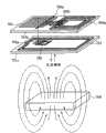
例如,图16示出第一天线电路、第二天线电路和增强天线的位置,以及包括图13中结构的RFID的半导体器件中的天线形状。在图16中,将包括线圈形状的第一天线电路704和多个第二天线电路705a和705b设置在衬底701上,将增强天线722设置在衬底721上,并且将衬底701附接于721。For example, FIG. 16 shows the positions of the first antenna circuit, the second antenna circuit, and the booster antenna, and the shape of the antenna in the semiconductor device including the RFID of the structure in FIG. 13 . In FIG. 16, a
在图16中,当使得读取器/写入器706和增强天线722彼此靠近时,从读取器/写入器706产生的交流磁场经过环形(coiled)增强天线722,并且通过电磁感应在环形增强天线722的端子之间(在天线的一端和另一端之间)产生电动势。在环形增强天线722中,通过电磁感应产生电动势,并且从增强天线722自身产生交流磁场。然后,从增强天线722产生的交流磁场通过环形第一天线电路704,并且通过电磁感应在第一天线电路704的端子之间(在天线的一端和另一端之间)产生电动势。通过电动势在读取器/写入器706和第一天线电路704之间发送/接收数据。In FIG. 16, when the reader/
图17示出与图16不同的结构。FIG. 17 shows a structure different from FIG. 16 .
图17示出设置有第一天线电路704和包括第一信号处理电路的芯片702a的衬底701a,与设置有电池703、多个第二天线电路705a和705b、包括第二信号处理电路的芯片702b的衬底701b彼此重叠的结构。17 shows a
在图17中,当读取器/写入器706和增强天线彼此靠近时,从读取器/写入器706产生的交流磁场经过环形增强天线722,并且通过电磁感应在环形增强天线722的端子之间(在天线的一端和另一端之间)产生电动势。在环形增强天线722中,通过电磁感应产生电动势,并且从增强天线722自身产生交流磁场。然后,从增强天线722产生的交流磁场通过环形第一天线电路704,并且通过电磁感应在第一天线电路704的端子之间(在天线的一端和另一端之间)产生电动势。通过电动势在读取器/写入器706和第一天线电路704之间发送/接收数据。In FIG. 17, when the reader/
可通过与电池703和增强天线722附接的方式设置在本实施方式中描述的半导体器件。例如,如图18所示,将设置有第一天线电路704、第二天线电路705a和705b、和包括第一信号处理电路和第二信号处理电路的芯片702的衬底701,与设置有电池703和增强天线722的衬底721彼此附接。在这种情况下,示出将电池703附接于衬底701的正面(在上面形成芯片702的一侧),以及将设置有增强天线722的衬底721附接于衬底701的背面的实例。The semiconductor device described in this embodiment mode can be provided by being attached with the
因此,在不同衬底上单独形成用于向/从读取器/写入器发送/接收信号的芯片和天线以及用于对电池充电的芯片和天线之后,将衬底彼此附接,从而可形成具有更大形状的天线和电池。Therefore, after separately forming a chip and an antenna for transmitting/receiving signals to/from a reader/writer and a chip and an antenna for charging a battery on different substrates, the substrates are attached to each other, so that Antennas and batteries are formed with larger shapes.
在本实施方式中可允许第一天线电路、第二天线电路和增强天线的设计布局,只要将这些天线设置为使得交流磁场通过每一个天线线圈即可。如图17所示,将第一天线电路或第二天线电路设置在具有较大面积的增强天线的内部,从而可实现有效布局。因此,由于电池等可构成较大面积,所以可增加天线的线圈,因此布局更好。In this embodiment, the design layout of the first antenna circuit, the second antenna circuit and the booster antenna is allowed, as long as these antennas are arranged so that the AC magnetic field passes through each antenna coil. As shown in FIG. 17, the first antenna circuit or the second antenna circuit is provided inside a booster antenna having a larger area, thereby enabling efficient layout. Therefore, since the battery and the like can constitute a larger area, the coils of the antenna can be increased, and thus the layout is better.
如上所述,包括本发明的RFID的半导体器件具有电池;因此,它可防止由于电池随时间衰退而使得发送/接收各个信息的电力变低。此外,本发明的半导体器件具有接收用以向电池供应电力的信号的天线。因此,半导体器件可通过利用外部电磁波作为驱动半导体器件的电源而无需直接连接充电器的方式对电池充电。因此,能够在不需要检查电池的剩余容量或电池改变(这是在有源RFID的情况下所必须的)的情况下继续使用半导体器件。此外,将驱动RFID的电力始终保存在电池中,从而可获得足够运行RFID的电力,以及可扩展与读取器/写入器的通信距离。As described above, the semiconductor device including the RFID of the present invention has a battery; therefore, it can prevent the power to transmit/receive each information from becoming low due to the deterioration of the battery over time. Furthermore, the semiconductor device of the present invention has an antenna for receiving a signal for supplying electric power to a battery. Accordingly, the semiconductor device can charge the battery by using external electromagnetic waves as a power source for driving the semiconductor device without directly connecting the charger. Therefore, it is possible to continue using the semiconductor device without checking the remaining capacity of the battery or changing the battery which is necessary in the case of the active RFID. In addition, the power to drive the RFID is always kept in the battery, so that enough power can be obtained to run the RFID, and the communication distance with the reader/writer can be extended.
除了实施方式1的结构的元件之外,本实施方式的结构包括增强天线。因此,可在RFID和读取器/写入器之间进一步可靠地发送/接收数据,并且RFID可进一步可靠地接收外部无线电信号。In addition to the elements of the structure of
应注意,可结合本说明书中的其他实施方式来实现本实施方式。It should be noted that this embodiment mode can be implemented in combination with other embodiment modes in this specification.
(实施方式3)(Embodiment 3)
在本实施方式中,参照附图说明在上述实施方式中描述的半导体器件的制造方法的实例。In this embodiment mode, an example of the manufacturing method of the semiconductor device described in the above embodiment mode is explained with reference to the drawings.
首先,参照图19A,在衬底1901的一个侧面上形成在其间插入有绝缘膜1902的剥离层1903。随后,将用作基础膜(base film)的绝缘膜1904与半导体膜1905(例如,包含非晶硅的膜)堆叠。应注意,可依次形成绝缘膜1902、剥离层1903、绝缘膜1904、和半导体膜1905。First, referring to FIG. 19A , a
作为衬底1901,可使用玻璃衬底、石英衬底、金属衬底(例如陶瓷衬底或不锈钢衬底)、或例如Si衬底的半导体衬底。可选择地,可使用由聚对苯二甲酸乙二醇酯(PET)、聚萘二甲酸乙二酯(PNT)、聚醚砜(PES)、丙烯酸等形成的衬底作为塑料衬底。应注意,在该步骤中,将剥离层1903设置在其间插入有绝缘膜1902的衬底1901的整个表面上;然而,在衬底1901的整个表面上设置剥离层之后,可通过使用光刻方法选择地设置剥离层1303。As the
通过CVD方法、溅射方法等,由绝缘材料(例如,氧化硅、氮化硅、氧氮化硅(SiOxNy,其中x>y>0)或氮氧化硅(SiNxOy,其中x>y>0))形成绝缘膜1902和1904。例如,在绝缘膜1902和1904均具有双层结构的情况下,则可形成氮氧化硅膜作为第一绝缘膜,形成氧氮化硅膜作为第二绝缘膜。或者,可形成氮化硅膜作为第一绝缘膜,形成氧化硅膜作为第二绝缘膜。绝缘层1902用作防止衬底1901中的杂质元素混入剥离层1903或混入其上形成的单元的阻挡层。绝缘层1904用作防止衬底1901和剥离层1903中的杂质元素混入在衬底1901和剥离层1903上形成的单元的阻挡层。通过以这样方式形成均用作阻挡层的绝缘层1902和1904,可防止在衬底1901中的碱土金属或碱金属(例如Na)和剥离层1903中包含的杂质元素对于在衬底1901和剥离层1903上形成的单元产生不利影响。在将石英用于衬底1901的情况下,可省略绝缘膜1902和1904。By CVD method, sputtering method, etc., an insulating material (for example, silicon oxide, silicon nitride, silicon oxynitride (SiOx Ny , where x>y>0) or silicon oxynitride (SiNx Oy , where x>y>0)) Insulating
作为剥离层1903,可使用金属膜、金属膜和金属氧化物膜的堆叠层结构等。金属膜可形成为从下述选择的元素或包含下述元素作为其主要成分的合金材料或混合材料的一层膜或叠层膜,其中所述元素包括:钨(W)、钼(Mo)、钛(Ti)、钽(Ta)、铌(Nb)、镍(Ni)、钴(Co)、锆(Zr)、锌(Zn)、钌(Ru)、铑(Rh)、钯(Pd)、锇(Os)和铱(Ir)。可通过溅射方法、各种CVD方法(例如等离子体CVD方法)等形成金属膜。作为金属膜和金属氧化物膜的叠层结构,在形成上述金属膜之后,可通过在氧气氛或N2O气氛中进行等离子体处理或在氧气氛或N2O气氛中进行热处理的方式,在金属膜的表面上形成金属膜的氧化物或氧氮化物。例如,在通过溅射方法、CVD方法等将钨膜形成为金属膜的情况下,可通过在钨膜上执行等离子体处理的方式在钨膜的表面上形成氧化钨形成的金属氧化物膜。在这种情况下,将钨的氧化物表示为WOx,其中x是2至3。还存在x=2(WO2),x=2.5(W2O5),x=2.75(W4O11),x=3(WO3)等。在形成钨的氧化物时,没有特别限制x的值,并且可根据蚀刻速率等确定形成哪种氧化物。或者,例如,在形成金属膜(例如钨)之后,可通过溅射方法在金属膜上形成氧化硅(SiO2)等的绝缘膜,并在金属膜上形成金属氧化物(例如,在钨上的钨氧化物)。此外,作为等离子体处理,例如,可执行上述的高密度等离子体处理。代替金属氧化物膜,可以使用金属氮化物或金属氧氮化物。在这种情况下,对于金属膜在氮气氛或氮氧气氛中进行等离子体处理或热处理。As the
通过溅射方法、LPCVD方法、等离子体CVD方法等将非晶半导体膜1905形成为具有25至200nm(优选地30至150nm)的厚度。The
接下来,如图19B所示,通过激光照射使半导体膜1905结晶。应注意,可通过将激光照射方法与使用RTA或退火炉的热结晶方法或与使用促进结晶的金属元素的热结晶方法等结合的方法,使非晶半导体膜1905结晶。之后,蚀刻所获得的结晶半导体膜以使其具有期望形状,从而形成结晶半导体膜1905a至1905f。然后形成栅极绝缘膜1906,以覆盖结晶半导体膜1905a至1905f。Next, as shown in FIG. 19B, the
通过CVD方法、溅射方法等,由绝缘材料(例如,氧化硅、氮化硅、氧氮化硅(SiOxNy,其中x>y>0)或氮氧化硅(SiNxOy,其中x>y>0))形成栅极绝缘膜1906。例如,在栅极绝缘膜1906具有双层结构的情况下,则可形成氧氮化硅膜作为第一绝缘膜,形成氮氧化硅膜作为第二绝缘膜。或者,可形成氧化硅膜作为第一绝缘膜,形成氮化硅膜作为第二绝缘膜。By CVD method, sputtering method, etc., an insulating material (for example, silicon oxide, silicon nitride, silicon oxynitride (SiOx Ny , where x>y>0) or silicon oxynitride (SiNx Oy , where x>y>0)) A
以下简单描述结晶半导体膜1905a至1905f的制造步骤实例。首先,通过等离子体CVD方法形成具有50至60nm厚度的非晶半导体膜。接下来,在非晶半导体膜上保留包含用以促进结晶的金属元素(即镍)的溶液,并在非晶半导体膜上执行脱氢处理(在500℃,持续1小时)和热结晶处理(在550℃,持续4小时),从而形成结晶半导体膜。随后,通过用激光照射结晶半导体膜并使用光刻方法,形成结晶半导体膜1905a至1905f。应注意,可不使用促进结晶的金属元素进行热结晶,而仅通过激光照射使非晶半导体膜结晶。An example of manufacturing steps of the
作为用于结晶的激光振荡器,可使用连续波激光束(CW激光束)或脉冲波激光束(脉冲激光束)。作为这里可使用的激光束,可使用从以下中的一个或多个激光器发射的激光束,包括:气体激光器,例如Ar激光器、Kr激光器或受激准分子激光器;其介质是单晶YAG、YVO4、镁橄榄石(Mg2SiO4)、YalO3、GdVO4、或增加有Nd、Yb、Cr、Ti、Ho、Er、Tm和Ta中一个或多个作为杂质的多晶(陶瓷)YAG、Y2O3、YVO4、YAlO3或GdVO4的激光器;玻璃激光器;红宝石激光器;紫翠玉激光器;钛宝石(Ti:sapphire)激光器;铜蒸气激光器;或金蒸气激光器。在使用这种激光束的基波或基波的第二至第四谐波时,可获得具有较大粒度的结晶。例如,可使用Nd:YVO4激光(1064nm的基波)的第二谐波(532nm)或第三谐波(355nm)。在这种情况下,需要大约0.01至100MW/cm2(优选地,0.1至10MW/cm2)的能量密度。以大约10至2000cm/sec(秒)的扫描速率进行照射。应注意,使用单晶YAG、YVO4、镁橄榄石(Mg2SiO4)、YalO3、GdVO4、或增加有Nd、Yb、Cr、Ti、Ho、Er、Tm和Ta中一个或多个作为杂质的多晶(陶瓷)YAG、Y2O3、YVO4、YAlO3或GdVO4作为介质的激光器;Ar离子激光器;或钛宝石激光器可连续振荡。此外,可通过执行Q开关操作、模式锁定等,以10MHz或更高的重复速率执行其脉冲振荡。在以10MHz或更高的重复速率对激光束进行振荡的情况下,在通过激光器熔化半导体膜之后并且在其固化之前,用下一个脉冲照射半导体膜。因此,与使用以较低重复速率的脉冲激光的情况不同,可以在半导体膜中连续移动固体-液体界面,从而可获得在扫描方向上连续生长的晶粒。As a laser oscillator used for crystallization, a continuous wave laser beam (CW laser beam) or a pulse wave laser beam (pulse laser beam) can be used. As the laser beam usable here, laser beams emitted from one or more of the following can be used, including: gas lasers such as Ar lasers, Kr lasers, or excimer lasers; the medium of which is single crystal YAG, YVO4. Forsterite (Mg2 SiO4 ), YalO3 , GdVO4 , or polycrystalline (ceramic) YAG with one or more of Nd, Yb, Cr, Ti, Ho, Er, Tm and Ta added as impurities , Y2 O3 , YVO4 , YAlO3 or GdVO4 lasers; glass lasers; ruby lasers; alexandrite lasers; titanium sapphire (Ti: sapphire) lasers; copper vapor lasers; or gold vapor lasers. When using the fundamental wave or the second to fourth harmonics of the fundamental wave of such a laser beam, crystals with a larger grain size can be obtained. For example, the second harmonic (532 nm) or third harmonic (355 nm) of a Nd:YVO4 laser (1064 nm fundamental) can be used. In this case, an energy density of about 0.01 to 100 MW/cm2 (preferably, 0.1 to 10 MW/cm2 ) is required. Irradiation is performed at a scan rate of about 10 to 2000 cm/sec (second). It should be noted that the use of single crystal YAG, YVO4 , forsterite (Mg2 SiO4 ), YalO3 , GdVO4 , or one or more of Nd, Yb, Cr, Ti, Ho, Er, Tm, and Ta Lasers with polycrystalline (ceramic) YAG, Y2 O3 , YVO4 , YAlO3 , or GdVO4 as impurities; Ar ion lasers; or titanium sapphire lasers can continuously oscillate. In addition, its pulse oscillation can be performed at a repetition rate of 10MHz or higher by performing Q-switching operation, mode lock, etc. In the case of oscillating the laser beam at a repetition rate of 10 MHz or higher, after the semiconductor film is melted by the laser and before it is solidified, the semiconductor film is irradiated with the next pulse. Therefore, unlike the case of using pulsed laser light at a lower repetition rate, the solid-liquid interface can be continuously moved in the semiconductor film, so that continuous growth of crystal grains in the scanning direction can be obtained.
可选择地,可通过在半导体膜1905a至1905f上进行上述高密度等离子体处理以氧化或氮化表面的方式形成栅极绝缘膜1906。例如,通过引入稀有气体(例如,He、Ar、Kr或Xe)和氧、氧化氮(NO2)、氨、氮、氢等混合气体的等离子体处理形成该膜。在通过引入微波执行在这种情况下的等离子体的激发时,可以以较低电子温度产生高密度等离子体。可通过这种高密度等离子体产生的氧基(存在包括OH基的情况)或氮基(存在包括NH基的情况)氧化或氮化半导体膜的表面。Alternatively, the
通过使用这种高密度等离子体处理,在半导体膜上形成具有1至20nm(典型地,5至10nm)厚度的绝缘膜。由于在这种情况下的反应是固体阶段的反应,所以在绝缘膜和半导体膜之间的界面状态密度可以很低。由于这种高密度等离子体处理直接氧化(或氮化)半导体膜(晶体硅、或多晶硅),所以理想地,在其厚度方面形成的绝缘膜厚度的不均匀度极低。此外,即使在晶体硅的晶粒边界也没有进行强氧化,从而可得到很有利的条件。即,通过这里所示的高密度等离子体处理对半导体膜的表面进行固体阶段氧化,可形成具有高度均匀和低界面状态密度的绝缘膜,而不会在晶粒边界出现异常的氧化反应。By using such high-density plasma treatment, an insulating film having a thickness of 1 to 20 nm (typically, 5 to 10 nm) is formed on the semiconductor film. Since the reaction in this case is a solid phase reaction, the interface state density between the insulating film and the semiconductor film can be low. Since this high-density plasma treatment directly oxidizes (or nitrides) a semiconductor film (crystalline silicon, or polysilicon), ideally, an insulating film is formed with extremely low unevenness in its thickness. In addition, strong oxidation does not proceed even at the grain boundaries of crystalline silicon, so that very favorable conditions can be obtained. That is, solid-phase oxidation of the surface of a semiconductor film by the high-density plasma treatment shown here can form an insulating film with a high degree of uniformity and low interface state density without abnormal oxidation reactions at grain boundaries.
作为栅极绝缘膜1906,可单独使用由高密度等离子体处理形成的绝缘膜,或使用等离子体或热反应通过CVD方法在其上形成氧化硅、氧氮化硅、氮化硅等的绝缘膜,以形成叠层。在任意情况下,包括由一部分栅极绝缘膜或整个栅极绝缘膜中的高密度等离子体形成的绝缘膜的晶体管可减少不均匀特征。As the
此外,通过连续波激光束或以10MHz或更高重复速率振荡的激光束照射半导体膜并以对半导体膜结晶的一个方向扫描半导体膜,从而获得具有结晶在激光束的扫描方向上生长的特性的半导体膜1905a至1905f。在设置晶体管使得扫描方向与沟道长度方向(在形成沟道形成区域时载流子流动的方向)对准并且使用上述栅极绝缘层时,可获得具有较少变化特征和较高电场效应迁移率的薄膜晶体管(TFT)。Further, by irradiating the semiconductor film with a continuous wave laser beam or a laser beam oscillating at a repetition rate of 10 MHz or higher and scanning the semiconductor film in one direction to the crystallization of the semiconductor film, a film having a property that the crystal grows in the scanning direction of the laser beam is obtained
接下来,在栅极绝缘膜1906上堆叠第一导电膜和第二导电膜。这里,通过CVD方法、溅射方法等形成具有20至100nm厚度的第一导电膜,形成具有100至400nm厚度的第二导电膜。使用从钽(Ta)、钨(W)、钛(Ti)、钼(Mo)、铝(Al)、铜(Cu)、铬(Cr)、铌(Nb)等中选择的元素,或包含上述元素作为其主要成分的合金材料或混合材料来形成第一导电膜和第二导电膜。或者,使用掺杂有例如磷的杂质元素的多晶硅代表的半导体材料形成所述导电膜。作为第一导电膜和第二导电膜的组合的实例,可给出氮化钽膜和钨膜、氮化钨膜和钨膜、氮化钼膜和钼膜等。由于钨和氮化钽具有较高热阻抗,所以可以在形成第一导电膜和第二导电膜之后执行用于热激发的热处理。此外,在使用三层结构代替双层结构的情况下,优选地可采用包括钼膜、铝膜和钼膜的叠层结构。Next, a first conductive film and a second conductive film are stacked on the
接下来,使用光刻方法形成抗蚀剂掩模,执行用于形成栅电极和栅极线的蚀刻处理,从而在半导体膜1905a至1905f上形成栅电极1907。这里,示出栅电极1907具有第一导电膜1907a和第二导电膜1907b的叠层结构的实例。Next, a resist mask is formed using a photolithography method, etching processing for forming gate electrodes and gate lines is performed, thereby forming
接下来,如图19C所示,将栅电极1907用作掩模,并通过离子掺杂方法或离子注入方法以较低浓度对半导体膜1905a至1905f添加用于赋予n型导电性的杂质元素,然后通过光刻方法选择性形成抗蚀剂掩模,并且以较高能度添加用于赋予p型导电性的杂质元素。作为n型杂质元素,可使用磷(P)、砷(As)。作为p型杂质元素,可使用硼(B)、铝(Al)、镓(Ga)等。这里,将磷(P)用作赋予n型导电性的杂质元素,并且将其选择性地以1×10¹⁵至1×10¹⁹/cm3的浓度引入半导体膜1905a至1905f,从而形成n型杂质区1908。此外,将硼(B)用作赋予p型导电性的杂质元素,并且将其选择性地以1×1019至1×1020/cm3的浓度引入半导体膜1905c至1905e,从而形成p型杂质区1909。Next, as shown in FIG. 19C, the
接下来,形成绝缘膜,以覆盖栅极绝缘膜1906和栅电极1907。通过等离子体CVD方法、溅射方法等形成绝缘膜,作为包含无机材料(例如硅、硅氧化物或硅氮化物)或有机材料(例如有机树脂)的一层膜或叠层膜。接下来,通过各向异性蚀刻(即主要沿垂直方向蚀刻)来选择性蚀刻绝缘膜,从而形成与栅电极1907的侧表面接触的绝缘膜1910(还称为侧壁)。在形成LDD(轻掺杂漏极)区时,绝缘膜1910用作掺杂掩模。Next, an insulating film is formed so as to cover the
接下来,使用通过光刻方法形成的抗蚀剂掩模、栅电极1907、和绝缘膜1910作为掩模,以高浓度向半导体膜1905a、1905b、1905d和1905f添加赋予n型导电性的杂质元素,从而形成n型杂质区1911。这里,将磷(P)用作赋予n型导电性的杂质元素,并将其选择性地以1×10¹⁵至1×10¹⁹/cm3的浓度引入半导体膜1905a、1905b、1905d和1905f,从而形成具有比n型杂质区1908更高浓度的n型杂质区1911。Next, using the resist mask formed by the photolithography method, the
通过上述步骤形成n沟道薄膜晶体管1900a、1900b、1900d和1900f和p沟道薄膜晶体管1900c和1900e。The n-channel
应注意,在n沟道薄膜晶体管1900a中,在与栅电极1907重叠的半导体膜1905a的区域中形成沟道形成区;在不与栅电极1907和绝缘膜1910重叠的区域中形成杂质区1911,其形成源极区或漏极区;在与绝缘膜1910重叠的区域中形成轻掺杂漏极区(LDD区),并且所述轻掺杂漏极区(LDD区)在沟道形成区和杂质区1911之间。类似地,在n沟道薄膜晶体管1900b、1900d和1900f中形成沟道形成区、轻掺杂漏极区和杂质区1911。It should be noted that, in n-channel
在p沟道薄膜晶体管1900c中,在与栅电极1907重叠的半导体膜1905c的区域中形成沟道形成区;在不与栅电极1907重叠的区域中形成杂质区1909,其形成源极区或漏极区。类似地,在p沟道薄膜晶体管1900e中形成沟道形成区和杂质区1909。应注意,尽管p沟道薄膜晶体管1900c和1900e均没有设置LDD区,但是可采用对p沟道薄膜晶体管设置LDD区,或对n沟道薄膜晶体管不设置LDD区的结构。In the p-channel
接下来,形成一层或叠层的绝缘膜,以覆盖半导体膜1905a至1905f、栅电极1907等;从而在绝缘膜上形成导电膜1913,其与形成薄膜晶体管1900a至1900f的源极区或漏极区的杂质区1909和1911电连接。通过CVD方法、溅射方法、SOG方法、小滴排放(dropletdischarge)方法、丝网印刷方法等,使用无机材料(例如硅氧化物或硅氮化物)、有机材料(例如聚酰亚胺、聚酰胺、苯并环丁烯、丙烯酸、或环氧树脂)、硅氧烷材料形成一层或叠层的绝缘膜。这里,形成具有双层结构的绝缘膜。形成氮氧化硅膜作为第一绝缘膜1912a,形成氧氮化硅膜作为第二绝缘膜1912b。导电膜1913形成半导体膜1905a至1905f的源电极和漏电极。Next, a layer or a stack of insulating films is formed to cover the
应注意,在形成绝缘膜1912a和1912b之前或形成绝缘膜1912a和1912b的一个或多个薄膜之后,优选进行热处理,用于恢复半导体膜的结晶度,用于激活已增加到半导体膜中的杂质元素,或用于对半导体膜氢化。对于加热处理,可使用热退火、激光退火方法、RTA方法等。It should be noted that before forming the insulating
通过CVD方法、溅射方法等,使用从铝(Al)、钨(W)、钛(Ti)、钽(Ta)、钼(Mo)、镍(Ni)、铂(Pt)、铜(Cu)、金(Au)、银(Ag)、锰(Mn)、钕(Nd)、碳(C)或硅(Si)等中选择的元素,或包含上述元素之一作为其主要成分的合金材料或混合材料来形成一层或叠层的导电膜1913。包含铝作为其主要成分的合金材料对应于,例如包含铝作为其主要成分以及还包含镍的材料,或包含铝作为其主要成分以及还包含镍和包含碳与硅中的一个或两者的合金材料。优选地,导电膜1913采用,例如包括阻挡膜、铝硅(Al-Si)膜和阻挡膜的叠层结构,包括阻挡膜、铝硅(Al-Si)膜、氮化钛(TiN)膜和阻挡膜的叠层结构。应注意,阻挡膜对应于通过使用钛、钛的氮化物、钼或钼的氮化物形成的薄膜。具有较低阻抗和价格便宜的铝和铝硅是用于形成导电膜1913的最佳材料。此外,在形成上阻挡层和下阻挡层可防止产生铝或铝硅的突起。此外,在由高还原元素的钛形成阻挡膜的情况下,即使在结晶半导体膜上形成薄的自然氧化物膜,该自然氧化物膜的情况下也会被化学还原,从而可获得与结晶半导体膜的良好接触。Aluminum (Al), tungsten (W), titanium (Ti), tantalum (Ta), molybdenum (Mo), nickel (Ni), platinum (Pt), copper (Cu) , gold (Au), silver (Ag), manganese (Mn), neodymium (Nd), carbon (C) or silicon (Si), or an alloy material containing one of the above elements as its main component or The materials are mixed to form a
接下来,形成绝缘膜1914以覆盖导电膜1913,并且在绝缘膜1914上形成导电膜1915a和1915b,以电连接至导电膜1913,其分别形成半导体膜1905a和1905f的源电极或漏电极。此外,形成导电膜1916a和1916b,以电连接至导电膜1913,其分别形成半导体膜1905b和1905e的源电极或漏电极。应注意,可同时使用相同材料形成导电膜1915a、1915b、1916a和1916b。此外,可使用对于导电膜1913给出的任意材料形成导电膜1915a、1915b、1916a和1916b。Next, an insulating
随后,如图20B所示,形成导电膜1917a和1917b以电连接至导电膜1916a和1916b,并分别用作天线。这里,用作天线的导电膜1917a和1917b中的一个对应于在上述实施方式中描述的第一天线电路的天线,另一个对应于第二天线电路的天线。例如,当导电膜1917a是第一天线电路的天线并且导电膜1917b是第二天线电路的天线时,薄膜晶体管1900a至1900c用作在上述实施方式中所述的第一信号处理电路,薄膜晶体管1900d至1900f用作在上述实施方式中所述的第二信号处理电路。Subsequently, as shown in FIG. 20B,
绝缘膜1914可通过CVD方法、溅射方法等形成,以具有包括以下绝缘膜的单层结构或叠层结构,所述绝缘膜包括:包含氧或氮的绝缘膜,例如氧化硅(SiOx)、氮化硅(SiNx)、氧氮化硅(SiOxNy,x>y>0)或氮氧化硅(SiNxOy,x>y>0);包含碳的膜,例如DLC(类金刚石碳);有机材料构成的膜,例如环氧树脂、聚酰亚胺、聚酰胺、乙烯聚合物、苯酚、苯并环丁烯、或丙烯酸;或硅氧烷材料,例如硅氧烷树脂。硅氧烷材料是包括Si-O-Si键的材料。硅氧烷包括由硅(Si)和氧(O)的键形成的骨架结构(skeletal structure),其中包括至少包含氢的有机基(例如,烷基或芳烃)作为替代物。此外,可选择地,可使用氟基和至少包含氢的有机基作为替代物。The insulating
通过CVD方法、溅射方法、例如丝网印刷方法或凹版印刷方法的印刷方法、小滴排放方法、分配方法、电镀方法等使用导电材料形成导电膜1917a和1917b。该导电材料使用从铝(Al)、钛(Ti)、银(Ag)、铜(Cu)、金(Au)、铂(Pt)、镍(Ni)、钯(Pd)、钽(Ta)、或钼(Mo)中选择的元素,或包含上述元素之一作为其主要成分的合金材料或混合材料,形成为单层或叠层。The
例如,在通过丝网印刷方法形成用作天线的导电膜1917a和1917b的情况下,可通过选择性印刷在有机树脂中使得分别包括几纳米到几十微米粒度的导电粒子溶解或分散的导电胶来形成导电膜1917。作为导电粒子,可使用银(Ag)、金(Au)、铜(Cu)、镍(Ni)、铂(Pt)、钯(Pd)、钽(Ta)、钼(Mo)、钛(Ti)或卤化银中任意一个或多个金属的微粒或扩散式纳米粒子。此外,作为在导电胶中包括的有机树脂,可使用均用作金属粒子的粘结剂、溶剂、分散剂、或金属粒子涂层的一个或多个有机树脂。典型地,可使用例如环氧树脂或硅树脂的有机树脂。在形成导电膜时,优选地在涂覆导电胶之后进行烘烤。例如,在使用包含银作为主要成分的微粒(其粒度在1至100nm之间)作为导电胶的材料的情况下,可通过在150至300℃范围内的温度下烘烤的方式来硬化导电胶,因此可获得导电膜。可选择地,可使用包含焊料或无铅焊料作为主要成分的微粒。在这种情况下,优选地,使用具有20μm或更小粒度的微粒。焊料或无铅焊料具有例如低成本的优点。For example, in the case of forming the
在随后的步骤中,导电膜1915a和1915b均可用作在本实施方式的半导体器件中包括的电池电连接的配线。当形成用作天线的导电膜1917a和1917b时,可形成另一个导电膜以电连接至导电膜1915a和1915b,并且可用作连接至电池的配线。应注意,在图20B中的导电膜1917a和1917b分别对应于在实施方式1中所述的第一天线电路和第二天线电路。In subsequent steps, both the
接下来,如图20C所示,在形成绝缘膜1918以覆盖导电膜1917a和1917b之后,将包括薄膜晶体管1900a至1900f、导电膜1917a和1917b等的层(以下称为“单元形成层1919”)从衬底1901剥离。这里,在没有形成薄膜晶体管1900a至1900f的区域中通过激光(例如紫外光)照射形成开口,然后可使用物理力将单元形成层1919从衬底1901剥离。可选择地,在将单元形成层1919从衬底1901剥离之前,可将蚀刻剂引入所形成的开口中;从而去除剥离层1903。作为蚀刻剂,可使用包含卤素氟化物或卤素互化物的气体或液体。例如,将三氟化氯(ClF3)用作包含卤素氟化物的气体。因此,将单元形成层1919从衬底1901剥离。应注意,剥离层1903可部分地留下,而并非完全去除。因此,可减少蚀刻剂消耗量和缩短去除剥离层所需的处理时间。此外,即使在去除剥离层1903之后,也可能在衬底1901上留下单元形成层1919。另外,在剥离单元形成层1919之后重复使用衬底1901,可减少成本。Next, as shown in FIG. 20C, after an insulating
可通过CVD方法、溅射方法等形成绝缘膜1918,其具有包括以下材料的单层结构或叠层结构,所述材料包括:包含氧和/或氮的绝缘膜,例如氧化硅(SiOx)、氮化硅(SiNx)、氧氮化硅(SiOxNy,x>y>0)或氮氧化硅(SiNxOy,x>y>0);包含碳的膜,例如DLC(类金刚石碳);有机材料,例如环氧树脂、聚酰亚胺、聚酰胺、乙烯聚合物、苯酚、苯并环丁烯、或丙烯酸;或硅氧烷材料,例如硅氧烷树脂。The insulating
在本实施方式中,如图21A所示,在通过激光照射方式在单元形成层1919中形成开口之后,将第一板材1920附接在单元形成层1919的一个表面(暴露绝缘膜1918的表面),然后将单元形成层1919从衬底1901剥离。In the present embodiment, as shown in FIG. 21A , after openings are formed in the
接下来,如图21B所示,通过进行热处理和压力处理中的一个或两个处理将第二板材1921附接在单元形成层1919的另一表面(通过剥离所暴露的表面)。作为第一板材1920和第二板材1921,可使用热熔性膜等。Next, as shown in FIG. 21B , a
作为第一板材1920和第二板材1921,可使用在上面执行了用于防止静电的抗静电处理等的膜(以下称为抗静电膜)。作为抗静电膜,可给出在树脂中散布有防静电材料的膜,在其上附接有防静电材料的膜等作为实例。设置有防静电材料的膜可以是在其一个表面上设置有防静电材料的膜,或在其每一个表面上设置有防静电材料的膜。对于在其一个表面上设置有防静电材料的膜,可将该膜附接在所述层上,从而将防静电材料设置在膜的内侧或膜的外侧。应注意,防静电材料可设置在膜的整个表面上,或膜的一部分上。作为这里的防静电材料,可使用金属、铟锡氧化物(ITO)或表面活性剂,例如,两性表面活性剂、阳离子表面活性剂或非离子表面活性剂。可选择地,作为防静电材料,可使用基于其侧链具有羰基和季铵碱的交联共聚物的树脂材料。通过对膜附接、混合或涂覆这种材料,可形成防静电膜。使用防静电膜进行密封,因此可防止半导体元件在作为商品处理时由来自外部的静电等对半导体元件产生不利影响。As the
形成电池,以连接至导电膜1915a和1915b。在将单元形成层1919从衬底1901剥离之前,或在将单元形成层1919从衬底1301剥离之后(在图20B或图20C中的步骤,或图21A中的步骤),或在用第一板材和第二板材对单元形成层1919密封之后(在图21B中的步骤),可将电池连接至导电膜1915a和1915b。以下参照图22A至23B描述形成单元形成层1919和电池彼此连接的实例。A battery is formed to be connected to the
在图20B中,与用作天线的导电膜1917a和1917b同时形成分别与导电膜1915a和1915b电连接的导电膜1931a和1931b。在形成绝缘膜1918以覆盖导电膜1917a、1917b、1931a和1931b之后,形成开口1932a和1932b,从而暴露导电膜1931a和1931b的表面。随后,如图22A所示,在通过激光照射的方式在单元形成层1919中形成开口之后,将第一板材1920附接在单元形成层1919的一个表面(暴露绝缘膜1918的表面)上。然后将单元形成层1919从衬底1901剥离。In FIG. 20B,
接下来,如图22B所示,将第二板材1921附接在单元形成层1919的另一表面(通过剥离所暴露的表面)上,然后将单元形成层1919从第一板材1920剥离。因此,这里使用具有弱粘合性的第一板材1920。然后,选择性形成通过开口1932a和1932b与导电膜1931a和1931b电连接的导电膜1934a和1934b。Next, as shown in FIG. 22B , a
通过CVD方法、溅射方法、例如丝网印刷方法或凹版印刷方法的印刷方法、小滴排放方法、分配方法、电镀方法等使用导电材料形成用作天线的导电膜1934a和1934b。该导电材料是使用从铝(Al)、钛(Ti)、银(Ag)、铜(Cu)、金(Au)、铂(Pt)、镍(Ni)、钯(Pd)、钽(Ta)、和钼(Mo)中选择的元素,或包含上述元素之一作为其主要成分的合金材料或混合材料形成的,并具有单层结构或叠层结构。The
应注意,这里描述了在将单元形成层1919从衬底1901剥离之后,形成导电膜1934a和1934b的实例。可选择地,也可以在形成导电膜1934a和1934b之后将单元形成层1919从衬底1901剥离。It should be noted that an example in which the
随后,如图23A所示,在衬底上形成多个单元时,对单元形成层1919的每个单元进行切断。可使用激光照射装置、切割装置、划割装置等进行切断。这里,通过激光照射对于一个衬底上形成的多个单元中的每一个进行切断。Subsequently, as shown in FIG. 23A , when a plurality of cells are formed on the substrate, cutting is performed for each cell of the
接下来,如图23B所示,将切断的单元电连接至电池的连接端子。这里,将设置在单元形成层1919上的导电膜1934a和1934b分别连接至设置在衬底1935上的作为连接端子的导电膜1936a和1936b。这里,示出这样的情况,即通过使用粘性材料,例如各向异性导电膜(ACF)或各向异性导电胶(ACP)将导电膜1934a和1936a,或导电膜1934b和1936b压力接合的方式,使得彼此电连接。在这种情况下,示出使用在粘性树脂1937中包含的导电粒子1938进行连接的实例。可选择地,可使用例如银胶、铜胶、或碳胶的导电粘合剂,或焊料接合等进行连接。Next, as shown in FIG. 23B , the cut-off cell is electrically connected to the connection terminal of the battery. Here, the
在电池大于单元的情况下,如图22A至23B所示,在一个衬底上形成多个单元,并将已经切断的单元连接至电池。因此,可增加在一个衬底上可形成的单元数目,从而能够以低成本制造半导体器件。In the case of a battery larger than a cell, as shown in FIGS. 22A to 23B, a plurality of cells are formed on one substrate, and the cells that have been cut off are connected to the battery. Therefore, the number of cells formable on one substrate can be increased, enabling semiconductor devices to be manufactured at low cost.
随后,如上述实施方式所述,可将元素连接至增强天线。Subsequently, the element may be connected to a booster antenna as described in the above embodiments.
通过以上步骤,可制造半导体器件。应注意,在本实施方式中,示出在衬底上形成单元之后剥离例如薄膜晶体管的单元的处理。可选择地,可将衬底上形成的单元用作产品,而不需要从衬底剥离。此外,在剥离衬底上形成例如薄膜晶体管的单元之后,从上面形成单元的表面的对面对剥离衬底抛光,或者在使用例如Si的半导体衬底形成MOS晶体管之后,对半导体衬底抛光,从而可实现薄膜厚度和半导体器件尺寸的降低。Through the above steps, a semiconductor device can be manufactured. It should be noted that in this embodiment mode, a process of peeling off a cell such as a thin film transistor after forming the cell on the substrate is shown. Alternatively, the unit formed on the substrate can be used as a product without peeling from the substrate. Furthermore, after forming a cell such as a thin film transistor on the lift-off substrate, polishing the lift-off substrate from the opposite side of the surface on which the cell is formed, or polishing the semiconductor substrate after forming a MOS transistor using a semiconductor substrate such as Si, Thereby, reduction in film thickness and size of semiconductor devices can be achieved.
应注意,可结合本说明书中任意其他实施方式来实现本实施方式。It should be noted that this embodiment mode can be implemented in combination with any other embodiment mode in this specification.
(实施方式4)(Embodiment 4)
在本实施方式中,参照附图描述与上述实施方式不同的半导体器件的实例及其制造方法。In this embodiment mode, an example of a semiconductor device different from the above-described embodiment mode and its manufacturing method are described with reference to the drawings.
首先,如图24A所示,在衬底2401的一个表面上,形成在其间插入有绝缘膜2402的剥离层2403。随后,对用作基膜的绝缘膜2404和绝缘膜2405进行堆叠。应注意,可以依次形成绝缘膜2402、剥离层2403、绝缘膜2404和半导体膜2405。First, as shown in FIG. 24A, on one surface of a
可形成导电膜2405,作为从下述选择的元素或包含下述元素作为其主要成分的合金材料或混合材料的一层膜或叠层膜,其中所述元素包括:钨(W)、钼(Mo)、钛(Ti)、钽(Ta)、铌(Nb)、镍(Ni)、钴(Co)、锆(Zr)、锌(Zn)、钌(Ru)、铑(Rh)、钯(Pd)、锇(Os)和铱(Ir)。可通过溅射方法、各种CVD方法(例如等离子体CVD方法)等形成所述膜。The conductive film 2405 can be formed as a single film or laminated film of an element selected from tungsten (W), molybdenum ( Mo), titanium (Ti), tantalum (Ta), niobium (Nb), nickel (Ni), cobalt (Co), zirconium (Zr), zinc (Zn), ruthenium (Ru), rhodium (Rh), palladium ( Pd), osmium (Os) and iridium (Ir). The film can be formed by a sputtering method, various CVD methods such as a plasma CVD method, or the like.
可以通过分别使用在先前实施方式中描述的衬底1901、绝缘膜1902、剥离层1903和绝缘膜1904的材料来形成衬底2401、绝缘膜2402、剥离层2403和绝缘膜2404。The
接下来,如图24B所示,选择性蚀刻导电膜2405,以形成导电膜2405a至2405e,并使得绝缘膜2406和2407堆叠,以覆盖导电膜2405a至2405e。Next, as shown in FIG. 24B, the conductive film 2405 is selectively etched to form
通过CVD方法、溅射方法等由绝缘材料(例如,氧化硅、氮化硅、氧氮化硅(SiOxNy,x>y>0)或氮氧化硅(SiNxOy,x>y>0))形成绝缘膜1806和绝缘膜1807。例如,可使用氮氧化硅形成绝缘膜2406,可使用氧氮化硅形成绝缘膜2407。这里描述了形成具有双层结构的绝缘膜的实例。可选择地,也可以仅设置绝缘膜2406和2407中的一个,或可堆叠三个或更多绝缘膜。ByCVD method, sputtering method,etc. >0)) An insulating film 1806 and an insulating film 1807 are formed. For example, the insulating
接下来,如图24C所示,分别在导电膜2405a至2405d上选择性形成半导体膜2408a至2408d。这里,通过溅射方法、LPCVD方法、等离子体CVD方法等形成具有25至200nm厚度(优选地,30至150nm厚度)的非晶半导体膜(例如,非晶硅膜)。使非晶半导体膜结晶,然后,对其选择性蚀刻,以形成半导体膜2408a至2408d。作为半导体膜的材料、其结晶方法等,可使用在先前实施方式中所述的材料和方法。可依次形成绝缘膜2406和2407以及非晶半导体膜。Next, as shown in FIG. 24C,
应注意,在由于导电膜2405a至2405d而使得绝缘膜2407的表面具有凹凸的情况下,优选地对于所述表面进行平坦化处理,以使其变平。对于平坦化处理,可使用例如CMP方法的抛光处理。如图24A所示,通过执行例如CMP方法的抛光处理,可在包括平坦化表面的绝缘膜2407上形成半导体膜;因此,在使用半导体膜2408a至2408d形成单元时,可防止对于单元特性产生影响。It should be noted that, in the case where the surface of the insulating
接下来,如图24D所示,形成绝缘膜2409,以覆盖半导体膜2408a至2408d,并且在半导体膜2408a至2408c上选择性形成栅电极2410,然后将杂质元素添加至半导体膜2408a至2408d,以形成杂质区2411。添加用于赋予n型导电性或p型导电性的杂质元素作为杂质元素。作为n型杂质元素,可使用磷(P)、砷(As)等。作为p型杂质元素,可使用硼(B)、铝(Al)、镓(Ga)等。这里,将磷(P)用于赋予n型导电性的杂质元素,并将其以1×10¹⁹至1×10²⁰/cm3的浓度引入半导体膜2408a至2408d,从而形成n型杂质区2411。应注意,半导体器件的结构不限于此。可添加赋予p型导电性的杂质元素以形成p型杂质区,或可将赋予n型导电性和p型导电性的杂质元素选择性引入半导体膜2408a至2408d。Next, as shown in FIG. 24D, an insulating film 2409 is formed to cover the
通过以上步骤,如图24D所示,形成n沟道薄膜晶体管2400a至2400c和用作电容器的单元2400d。Through the above steps, as shown in FIG. 24D, n-channel thin film transistors 2400a to 2400c and a cell 2400d serving as a capacitor are formed.
在n沟道薄膜晶体管22400a中,在与栅电极2410重叠的半导体膜2408a的区域中形成沟道形成区,在不与栅电极2410重叠的区域中,形成杂质区2411,其形成源极区或漏极区,以与沟道形成区邻近。类似地,在n沟道薄膜晶体管2400b和2400c中,形成沟道形成区和杂质区2411,所述杂质区2411形成源极区或漏极区。In the n-channel thin film transistor 22400a, a channel formation region is formed in a region of the
在单元2400d中,通过导电膜2405d、绝缘膜2406和2407、和引入杂质元素的杂质区2411的堆叠结构形成电容器。In a cell 2400d, a capacitor is formed by a stacked structure of a
这里,描述了设置有n沟道薄膜晶体管2400a至2400c的实例。可选择地,可设置p沟道薄膜晶体管,或者,如上述实施方式所述,可设置与栅电极2410的侧表面接触的绝缘膜,并设置用于n沟道薄膜晶体管2400a至2400c的半导体膜的轻掺杂漏极区(LDD区)。Here, an example in which n-channel thin film transistors 2400a to 2400c are provided is described. Alternatively, a p-channel thin film transistor may be provided, or, as described in the above embodiment mode, an insulating film in contact with the side surface of the gate electrode 2410 may be provided, and a semiconductor film for the n-channel thin film transistors 2400a to 2400c may be provided. The lightly doped drain region (LDD region).
此外,如图27A所示,这里示出形成有大于半导体膜2408a至2408c的导电膜2405a至2405c的实例(形成导电膜2405a至2405c,以与薄膜晶体管2400a至2400c的沟道形成区和杂质区2411重叠),所述半导体器件的结构不限于此。例如,如图27B所示,可设置导电膜2405a至2405c,以与薄膜晶体管2400a至2400c的杂质区2411a的一部分和沟道形成区的整个表面重叠。或可设置导电膜2405a至2405c,以与杂质区2411的一部分和沟道形成区的一部分重叠,或可设置导电膜2405a至2405c,以仅与沟道形成区的一部分重叠。在这种情况下,优选地通过例如特别是CMP的抛光处理,以使得绝缘膜2407变平。In addition, as shown in FIG. 27A, there is shown an example where
应注意,导电膜2405a至2405c的设置能够防止薄膜晶体管的损坏、ESD(静电放电)、控制短沟道效应,以控制阈值电压等。此外,设置配线2405e作为在上层中形成的配线,从而可实现步骤的减少等。It should be noted that the provision of the
即,如果包括薄膜晶体管1800a至1800c的半导体器件弯曲,也可以通过形成与沟道形成区或杂质区重叠的导电膜来防止薄膜晶体管2400a至2400c的沟道形成区和杂质区扭曲;因此,也可防止薄膜晶体管2400a至2400c损坏。具体地,如图27B所示,与其间插入有半导体膜的栅电极相对而设置的半导体膜2405a至2405c的结构被形成得大于可采用的半导体膜,从而在晶体管中的半导体膜的物理强度增加。因此,可防止由于对晶体管施加的物理力而引起的晶体管损坏。That is, if the semiconductor device including the thin film transistors 1800a to 1800c is bent, the channel formation regions and the impurity regions of the thin film transistors 2400a to 2400c can also be prevented from twisting by forming a conductive film overlapping the channel formation regions or the impurity regions; therefore, also Damage to the thin film transistors 2400a to 2400c can be prevented. Specifically, as shown in FIG. 27B, the structure of the
此外,在制造半导体器件过程中,导电膜2405a至2405c是电荷的逃逸路径或电荷的扩散区,从而可减少电荷的局部聚集电场集中度;因此可防止ESD。In addition, the
此外,在薄膜晶体管2400a至2400c中,分别通过导电膜2405a至2405c阻止从漏极向源极的影响。因此,即使在沟道长度变短时,也可以防止短沟道效应。换句话说,可防止短沟道效应(晶体管的阈值电压Vth急剧偏移,以及低于阈值区域的漏极电流仅缓慢增加),其中所述短沟道效应是由于薄膜晶体管2400a至2400c的小型化造成的沟道长度减小而引起的。Furthermore, in the thin film transistors 2400a to 2400c, the influence from the drain to the source is blocked by the
此外,通过对导电膜2405a至2405c输入的电压,可控制薄膜晶体管2400a至2400c的阈值电压。In addition, the threshold voltages of the thin film transistors 2400a to 2400c can be controlled by the voltage input to the
图34B是示出在n型MOS晶体管的漏极电流和栅极电压之间的关系的曲线图。优选地,在栅极电压Vg为正的区域中,漏极电流Id足够大,在栅极电压Vg为0或更小的情况下,漏极电流为0。然而,通过曲线3404所示,即使当栅极电压Vg为0时,也可实际地仅流出漏极电流Id的IL的漏电流。由于半导体器件设置有许多晶体管,所以在一些情况下总漏电流不小。这种漏电流可增加半导体器件的待机功耗。换句话说,这种漏电流可增加在电池中存储的电力的消耗。FIG. 34B is a graph showing the relationship between the drain current and gate voltage of an n-type MOS transistor. Preferably, the drain current Id is sufficiently large in a region where the gate voltage Vg is positive, and is 0 in the case where the gate voltage Vg is 0 or less. However, as shown by the
向晶体管的沟道区添加很少量的杂质,从而将图34B中所示的曲线向右移动,因此可减少漏电流。然而,在这种情况下,存在这样的问题,即在Vg为正的情况下电流也减少,因此使得电路的频率特性恶化。Adding a very small amount of impurities to the channel region of the transistor shifts the curve shown in Figure 34B to the right, thus reducing leakage current. In this case, however, there is a problem that the current decreases even when Vg is positive, thus deteriorating the frequency characteristics of the circuit.
为了解决上述问题,在形成晶体管的半导体膜的上部和下部设置栅电极。即,半导体膜位于第一栅电极和第二栅电极之间。然后,对于第一栅电极施加逻辑信号,对于第二栅电极施加阈值控制信号,并且在半导体器件中形成的晶体管的阈值可通过第二栅电极的电位改变。在本实施方式中,可将导电膜2405a至2405c分别用于薄膜晶体管2400a至2400c的第二栅电极。In order to solve the above-mentioned problems, gate electrodes are provided on the upper and lower parts of the semiconductor film forming the transistor. That is, the semiconductor film is located between the first gate electrode and the second gate electrode. Then, a logic signal is applied to the first gate electrode, a threshold control signal is applied to the second gate electrode, and the threshold of the transistor formed in the semiconductor device can be changed by the potential of the second gate electrode. In this embodiment mode, the
图34A示出包括第一栅电极和第二栅电极的晶体管的Id-Vg特性。在图34A中,示出曲线3401至3403,曲线3402是在向第二栅电极施加正电压的情况下的曲线。在这种情况下,曲线向左偏移,并且流过更多电流。此外,曲线3401是在向第二栅电极施加0V电压的情况下的曲线。这种情况与传统实例相同。曲线3403是在向第二栅电极施加负电压的情况下的曲线。在这种情况下,曲线向右偏移,电流不容易流过,并且漏电流减少。因此,通过阈值控制功能设置本实施方式的半导体器件,并且晶体管的Id-Vg特性的曲线偏移,从而能够减少漏电流。FIG. 34A shows Id-Vg characteristics of a transistor including a first gate electrode and a second gate electrode. In FIG. 34A , curves 3401 to 3403 are shown, and a
应注意,可以在本实施方式中导电膜2405a至2405e的同时形成随后形成的天线电路。由于可减少步骤的数目和掩模的数目,所以优选地同时形成导电膜和天线电路。优选地,导电膜2405a和2405b还可用作半导体膜之间的配线。具体地,这里,可形成配线2405e作为用作天线的导电膜。It should be noted that an antenna circuit formed later may be formed simultaneously with the
接下来,如图25A所示,形成绝缘膜2412,以覆盖薄膜晶体管2400a至2400c和元素2400d,并且在绝缘膜2412上形成与杂质区2411电连接的导电膜2413,其中杂质区2411分别形成薄膜晶体管2400a至2400c的源极区或漏极区。Next, as shown in FIG. 25A, an insulating film 2412 is formed to cover the thin film transistors 2400a to 2400c and the element 2400d, and a
通过CVD方法、溅射方法、SOG方法、小滴排放方法、丝网印刷方法等,使用无机材料(例如硅氧化物或硅氮化物)、有机材料(例如聚酰亚胺、聚酰胺、苯并环丁烯、丙烯酸、或环氧树脂)、硅氧烷材料等形成一层或叠层的绝缘膜2412。By CVD method, sputtering method, SOG method, droplet discharge method, screen printing method, etc., using inorganic materials (such as silicon oxide or silicon nitride), organic materials (such as polyimide, polyamide, benzo Cyclobutene, acrylic, or epoxy resin), silicone material, etc. form a layer or stack of insulating films 2412 .
可使用如先前实施方式所述的导电膜1913的任意材料形成导电膜2413。The
接下来,如图25B所示,形成绝缘膜2414,以覆盖导电膜2413,并且在绝缘膜2414上形成与导电膜2413电连接的导电膜2415a和2415b,其中导电膜2413形成薄膜晶体管2400a至2400c的源极区或漏极区。之后,形成用作天线的导电膜2416a和2416b,以与导电膜2415a和2415b电连接。Next, as shown in FIG. 25B, an insulating film 2414 is formed to cover the
应注意,在图25B中的导电膜2416a和2416b分别对应于如实施方式1所述的第一天线电路和第二天线电路。It should be noted that the
随后,在形成绝缘膜2417以覆盖导电膜2416a和2416b之后,从衬底2401剥离包括薄膜晶体管2400a至2400c、单元2400d、导电膜2416a和2416b等的层(以下称为“单元形成层720”)。对于剥离处理,可使用在以上实施方式中所述的任意方法。Subsequently, after an insulating film 2417 is formed to cover the
这里,如图26A所示,在通过激光照射在单元形成层720中形成开口之后,将单元形成层720的一个表面(暴露绝缘膜2417的表面)附接到第一板材2418。然后,将单元形成层720从衬底2401剥离。Here, as shown in FIG. 26A , after openings are formed in the
接下来,如图26B所示,通过热处理和压力处理中的一个或两个处理将第二板材2419附接在单元形成层720的另一表面(通过剥离暴露的表面)。作为第一板材2418和第二板材2419,可使用热熔性膜等。Next, as shown in FIG. 26B , a
可通过上述处理制造半导体器件。应注意,在本实施方式中,可将形成电容器的元素2400d用作电池。此外,除了单元2400d之外,还可设置其他电池。在这种情况下,可使用在以上实施方式中所述的方法设置电池。A semiconductor device can be manufactured through the above-described processes. It should be noted that in this embodiment mode, the element 2400d forming a capacitor can be used as a battery. Furthermore, other batteries may be provided in addition to the unit 2400d. In this case, the battery can be provided using the method described in the above embodiments.
应注意,在本实施方式中描述的半导体器件不限于这里的描述。例如,可以在薄膜晶体管2400a至2400c下方设置用作电池或天线的导电膜。It should be noted that the semiconductor device described in this embodiment mode is not limited to the description here. For example, a conductive film serving as a battery or an antenna may be provided under the thin film transistors 2400a to 2400c.
图28A和28B中示出在薄膜晶体管2400a至2400c下方设置电池的实例。这里,设置导电膜2431a以与均用作薄膜晶体管2400b的源电极或漏电极的导电膜2413电连接,并且导电膜2431a连接至在单元形成层720下方(在将单元形成层720从衬底2401剥离时暴露的表面)形成的电池连接配线的导电膜2433a。这里,示出这样的实例,即设置薄膜晶体管代替形成电容器的单元2400d;设置导电膜2432a以与用作薄膜晶体管的源电极或漏电极的导电膜2413电连接;并且导电膜2431a连接至在单元形成层720下方(在将单元形成层720从衬底2401剥离时暴露的表面)形成的电池连接配线的导电膜2433a。An example in which a battery is provided under the thin film transistors 2400a to 2400c is shown in FIGS. 28A and 28B. Here, the
在这种情况下,在图25A中,为了暴露薄膜晶体管2400a至2400c的杂质区2411,在栅极绝缘膜2409和2412中形成第一开口,并且同时,在栅极绝缘膜2406、2407、2409和2412中形成第二开口。然后,设置导电膜2413以填充第一开口,并且设置导电膜2431a和2431b以填充第二开口。第一开口和第二开口可同时形成。当形成第一开口时,半导体膜2408a至2408c用作停止层,并且当形成第二开口时,剥离层2403用作停止层。随后,如图28A所示,形成用作天线的导电膜2416a和2416b,将单元形成层720从衬底2401剥离。In this case, in FIG. 25A, in order to expose the impurity regions 2411 of the thin film transistors 2400a to 2400c, first openings are formed in the gate insulating films 2409 and 2412, and at the same time, in the
接下来,如图28B所示,将导电膜2431a和2431b分别与在衬底2432上设置的用作电池连接配线的导电膜2433a和2433b连接,所述导电膜2431a和2431b是在从衬底2401剥离的单元形成层720的暴露表面上形成的。这里,示出这样的情况,即通过用粘着性的材料,例如各向异性导电膜(ACF)或各向异性导电胶(ACP)压力接合,将导电膜2431a和导电膜2433a,或导电膜2431b和导电膜2433b彼此电连接。在这种情况下,示出使用在粘性树脂2434中包含的导电粒子2435进行连接的实例。可选择地,可使用例如银胶、铜胶、或碳胶的导电粘合剂,或使用焊料接合等进行连接。Next, as shown in FIG. 28B, the
应注意,在本实施方式中,不仅可用作电池还可用作天线的导电膜设置在薄膜晶体管2400a至2400c下方。图29A和29B示出在薄膜晶体管2400a至2400c下方设置用作电池和天线的导电膜2416的实例。It should be noted that, in this embodiment mode, a conductive film that functions not only as a battery but also as an antenna is provided under the thin film transistors 2400a to 2400c. 29A and 29B show an example in which a conductive film 2416 serving as a battery and an antenna is provided under the thin film transistors 2400a to 2400c.
这里,设置导电膜2431c以与用作薄膜晶体管2400c的源电极或漏电极的导电膜2413电连接,并且导电膜2431c连接至在单元形成层2420下方用作天线的导电膜2416b(在从衬底2401剥离单元形成层720所暴露的表面)。此外,在本实例中,还如图28A和28B所示设置电池。Here, the
在这种情况下,在图25A中,为了暴露薄膜晶体管2400a至2400c的杂质区2411,在栅极绝缘膜2409和绝缘膜2412中形成第一开口。同时,如图29A所示,在绝缘膜2406、2407和2412,以及栅极绝缘膜2409中形成第二开口;设置导电膜2413以填充第一开口;和设置导电膜2431a至2431c以填充第二开口。第一开口和第二开口可同时形成。当形成第一开口时,半导体膜2408a至2408c用作停止层,并且当形成第二开口时,剥离层2403用作停止层。随后,如图28A所示形成用作天线的导电膜2416a之后,将单元形成层720从衬底2401剥离。In this case, in FIG. 25A, in order to expose the impurity regions 2411 of the thin film transistors 2400a to 2400c, first openings are formed in the gate insulating film 2409 and the insulating film 2412. Meanwhile, as shown in FIG. 29A, a second opening is formed in the insulating
然后,如图29B所示,分别将从衬底2401剥离的单元形成层2420的暴露表面上形成的导电膜2431a和2431b连接至在衬底2432上设置的用作电池连接配线的导电膜2433a和2433b。此外,在从衬底2401剥离的单元形成层720的暴露表面上形成的导电膜2431c与在衬底2436上设置的用作天线的导电膜2416b连接。Then, as shown in FIG. 29B, the
在电池或天线大于通过薄膜晶体管2400a至2400c设置的单元的情况下,如图28A至29B所示,优选地,单元形成层和电池或天线设置为彼此连接。在使用大于单元的电池或天线时,在衬底上形成多个单元,将切断的单元与电池或天线连接。因此,可以以最低成本制造半导体器件。In the case where the battery or the antenna is larger than the cell provided by the thin film transistors 2400a to 2400c, as shown in FIGS. 28A to 29B, it is preferable that the cell forming layer and the battery or the antenna are provided to be connected to each other. When using a battery or antenna that is larger than a unit, multiple units are formed on a substrate, and the cut-off units are connected to the battery or antenna. Therefore, semiconductor devices can be manufactured at the lowest cost.
应注意,可结合本说明书中的其他实施方式来实现本实施方式。It should be noted that this embodiment mode can be implemented in combination with other embodiment modes in this specification.
(实施方式5)(Embodiment 5)
在本实施方式中,将参照附图描述如上述实施方式所述的半导体器件中第一天线、第二天线、信号处理电路、电池和增强天线的连接结构。In this embodiment mode, the connection structure of the first antenna, the second antenna, the signal processing circuit, the battery, and the booster antenna in the semiconductor device as described in the above embodiment mode will be described with reference to the accompanying drawings.
首先,在图11A所示的附图中,半导体器件包括:信号处理电路9901、信号处理电路的上电极9902和下电极9903、电池9904、电池的侧电极9905、衬底9906、和天线电路9907。电池在侧部具有电极,天线电路在上部具有电极。此外,可依次堆叠电池9904、信号处理电路9901、和包括天线电路的衬底9906。First, in the drawing shown in FIG. 11A , the semiconductor device includes: a
应注意,参照附图指定本实施例中的上部、下部和侧部用于说明。因此,在实际连接中,通过每个部分的形状与附图的比较来指定和连接每个部分的位置。It should be noted that upper, lower, and side portions in the present embodiment are designated for description with reference to the drawings. Therefore, in the actual connection, the position of each part is specified and connected by comparing the shape of each part with the drawings.
应注意,在本实施方式中的天线电路9907对应于在上述实施方式中描述的第一天线电路和第二天线电路。此外,天线电路9907和信号处理电路9901在天线电路的端子部彼此连接。It should be noted that the
对于每个部分描述在本实施方式中描述的结构的连接。应注意,结构的实际连接的数目不限于此,并且通过假设在多个部分进行连接的方式进行描述。The connection of the structures described in this embodiment mode is described for each part. It should be noted that the number of actual connections of the structure is not limited thereto, and description is made assuming connections are made at a plurality of sections.
对于信号处理电路中的上电极和下电极的连接,它们可在上述实施方式中所述的图22B所示的晶体管的上部电连接,或者它们可在上述实施方式中所述的图29B所示的晶体管的下部电连接。此外,可通过溅射方法、电镀方法等形成通过侧面连接上电极和下电极的侧电极。As for the connection of the upper electrode and the lower electrode in the signal processing circuit, they can be electrically connected at the upper part of the transistor shown in FIG. 22B described in the above embodiment, or they can be connected as shown in FIG. The lower part of the transistor is electrically connected. In addition, side electrodes connecting the upper electrode and the lower electrode through side surfaces may be formed by a sputtering method, a plating method, or the like.
接下来,图11B示出与图11A不同的结构。在图11B所示的附图中,半导体器件包括:信号处理电路9901、信号处理电路的上电极9902和侧电极9913、电池9904、电池的侧电极9905、衬底9906、和天线电路9907。图11B所示的信号处理电路9901具有与电池侧面连接的上电极以及从电池侧面上的电极沿着信号处理电路的侧面通向衬底侧面的侧电极。电池在侧部具有电极,天线电路在上部具有电极。此外,依次堆叠电池9904、信号处理电路9901、和包括天线电路的衬底9906。Next, FIG. 11B shows a structure different from that of FIG. 11A. In the drawing shown in FIG. 11B , the semiconductor device includes: a
接下来,图11C示出与图11A和11B不同的结构。在图11C所示的附图中,半导体器件包括:信号处理电路9901、信号处理电路的上电极9902、电池9904、电池的侧电极9905、衬底9906、和增强天线9909。图11C中的信号处理电路9901具有与电池侧面连接的上电极。电池在侧部具有电极,增强天线在上部具有电极。此外,依次堆叠电池9904、信号处理电路9901、和包括增强天线的衬底9906。Next, Fig. 11C shows a structure different from Figs. 11A and 11B. In the drawing shown in FIG. 11C , the semiconductor device includes: a
应注意,在图11C中,在上述实施方式中所述的第一天线电路和第二天线电路设置有信号处理电路,这与图11A和11B所示的结构不同。It should be noted that in FIG. 11C , the first antenna circuit and the second antenna circuit described in the above embodiments are provided with signal processing circuits, which is different from the structures shown in FIGS. 11A and 11B .
接下来,图11D示出与图11A至11C不同的结构。在图11D所示的附图中,半导体器件包括:信号处理电路9901、信号处理电路的上电极9902和下电极9903、电池9904、电池的下电极9915、衬底9906、和天线电路9907。图11D中的信号处理电路9901具有上下电极。电池在下部具有电极,增强天线在上部具有电极。此外,依次堆叠电池9904、信号处理电路9901、和包括天线电路的衬底9906。Next, Fig. 11D shows a structure different from Figs. 11A to 11C. In the drawing shown in FIG. 11D , the semiconductor device includes: a
接下来,图11E示出与图11A至11D不同的结构。在图11E所示的附图中,半导体器件包括:信号处理电路9901、信号处理电路的上电极9902和侧电极9913、电池9904、电池的下电极9915、衬底9906、和天线电路9907。图11E中的信号处理电路9901具有与电池侧面连接的上电极以及从电池侧面上的电极沿着信号处理电路的侧面通向衬底侧面的侧电极。电池在下部具有电极,天线电路在上部具有电极。此外,依次堆叠电池9904、信号处理电路9901、和包括天线电路的衬底9906。Next, FIG. 11E shows a structure different from FIGS. 11A to 11D . In the drawing shown in FIG. 11E , the semiconductor device includes: a
接下来,图11F示出与图11A至11E不同的结构。在图11F所示的附图中,半导体器件包括:信号处理电路9901、信号处理电路的上电极9902、电池9904、电池的下电极9915、衬底9908、和增强天线9909。图11F中的信号处理电路9901具有与电池侧面连接的上电极。电池在下部具有电极,增强天线在上部具有电极。此外,依次堆叠电池9904、信号处理电路9901、和包括增强天线的衬底9908。Next, FIG. 11F shows a structure different from FIGS. 11A to 11E . In the drawing shown in FIG. 11F , the semiconductor device includes: a
应注意,在图11F中,在上述实施方式中所述的第一天线电路和第二天线电路设置有信号处理电路,这与图11A、11B、11D和11E所示的结构不同。It should be noted that in FIG. 11F , the first antenna circuit and the second antenna circuit described in the above embodiments are provided with signal processing circuits, which is different from the structures shown in FIGS. 11A , 11B, 11D, and 11E.
如上所述,对于本实施方式的天线电路、信号处理电路、电池和增强天线的连接结构可采用各种模式。通过应用图11A至11F所示的每个结构,天线电路、信号处理电路和电池可直接连接,因此不必通过将配线延伸到衬底的外围来连接它们。此外,通过调节天线电路、信号处理电路和电池的尺寸,优选地,可减小包括RFID的半导体器件的尺寸。As described above, various modes can be adopted for the connection structure of the antenna circuit, signal processing circuit, battery, and booster antenna of the present embodiment. By applying each of the structures shown in FIGS. 11A to 11F , the antenna circuit, the signal processing circuit, and the battery can be directly connected, so it is not necessary to connect them by extending wiring to the periphery of the substrate. Furthermore, by adjusting the sizes of the antenna circuit, the signal processing circuit, and the battery, preferably, the size of the semiconductor device including the RFID can be reduced.
应注意,可结合本说明书中的其他实施方式来实现本实施方式。It should be noted that this embodiment mode can be implemented in combination with other embodiment modes in this specification.
(实施方式6)(Embodiment 6)
在本实施方式中,描述用于对本发明的半导体器件充电的方法实例。In this embodiment mode, an example of a method for charging the semiconductor device of the present invention is described.
本实施方式的半导体器件具有图1中所示的半导体器件的结构,对其添加了充电和放电控制电路9301(图41)。充电和放电控制电路9301控制对电池104充电和放电的定时。The semiconductor device of this embodiment mode has the structure of the semiconductor device shown in FIG. 1 to which a charge and discharge control circuit 9301 ( FIG. 41 ) is added. The charging and discharging
例如,可通过充电和放电控制电路9301同时对电池104充电和放电。换句话说,可对电池提供从第二整流电路107输出的电力用于充电,而不管是否将电池104的电压用于信号处理电路103的电源。For example, the
此外,为了不对电池104过多充电,在电池104的电压到达一定电压时,充电和放电控制电路9301具有停止对电池104充电的功能。In addition, in order not to overcharge the
图37示出在这种情况下的流程图实例。以下,简单描述在图37中的流程图。Fig. 37 shows an example of a flowchart in this case. Hereinafter, the flowchart in Fig. 37 will be briefly described.
首先,第二天线电路102接收信号(步骤9401)。通过第二整流电路107对于由第二天线电路102接收的信号整流,以获得电力(步骤9402)。向充电和放电控制电路9301提供从第二整流电路107输出的电力。然后,充电和放电控制电路9301确定电池104的电压是否小于一定电压(步骤9403)。First, the
在该电压小于一定电压时,充电和放电控制电路9301在一定时间段提供从第二整流电路107输出的电力,以对电池充电(步骤9404)。在该电压等于一定电压或更大电压时(包括重复步骤9403和步骤9404,从而该电压到达一定电压或更大电压的情况),充电和放电控制电路9301不向电池104提供从第二整流电路107输出的电力(步骤9405)。每次由第二天线电路102接收到信号时执行这些操作。When the voltage is less than a certain voltage, the charge and
此外,充电和放电控制电路9301可具有在电池104的电压小于一定电压时对电池104充电的功能,以及在电池104的电压到达一定电压时停止对电池104充电的功能。In addition, the charging and discharging
图38示出这种情况的流程图实例。以下,简单描述图38中的流程图。Fig. 38 shows an example of a flowchart for this case. Hereinafter, the flowchart in Fig. 38 will be briefly described.
首先,第二天线电路102接收信号(步骤9501)。通过第二整流电路107对于由第二天线电路102接收的信号整流,以获得电力(步骤9502)。向充电和放电控制电路9301提供从第二整流电路107输出的电力。然后,充电和放电控制电路9301确定电池104的电压是否小于一定电压V1(步骤9503)。在该电压小于一定电压V1时,充电和放电控制电路9301提供从第二整流电路107输出的电力,从而电池的电压到达一定电压V2(应注意,V2>V1)(步骤9504)。在该电压等于一定电压V1或更大电压时(包括步骤9504中电池104的电压到达一定电压V1或更大电压的情况),充电和放电控制电路9301不向电池104提供从第二整流电路107输出的电力(步骤9505)。每次由第二天线电路102接收到信号时执行这些操作。First, the
可选择地,可向电池104充电或从电池104放电。即,在第一天线电路101没有接收到信号时,充电和放电控制电路9301使得能够对电池104充电,而在第一天线电路101接收到信号时,充电和放电控制电路9301停止对电池104充电,并且使得能够从电池104放电。Alternatively, the
图39示出这种情况的流程图实例。以下,简单描述图39中的流程图。Fig. 39 shows an example of a flowchart for this case. Hereinafter, the flowchart in Fig. 39 will be briefly described.
首先,第二天线电路102接收信号(步骤9601)。通过第二整流电路107对于由第二天线电路102接收的信号整流,以获得电力(步骤9602)。向充电和放电控制电路9301提供从第二整流电路107输出的电力。在第一天线电路101正在接收信号,例如从逻辑电路110向充电和放电控制电路9301发送信息的信号时(步骤9603),然后,充电和放电控制电路9301停止从第二整流电路107向电池104供应电力(步骤9404)。在第一天线电路101没有接收信号时,充电和放电控制电路9301提供从第二整流电路107输出的电力,以对电池充电,从而电池的电压到达一定电压(步骤9605和步骤9606)。在电池的电压到达一定电压时,充电和放电控制电路9301不向电池104提供从第二整流电路107输出的电力(步骤9604)。每次由第二天线电路102接收到信号时执行这些操作。First, the
此外,充电和放电控制电路9301可具有如下功能:由第一天线电路101接收信号以通过信号处理电路103处理,然后从第一天线电路101发送信号,之后以对应于电池104的消耗电量充电。In addition, the charging and discharging
图40示出这种情况的流程图实例。以下,简单描述图40中的流程图。Fig. 40 shows an example of a flowchart for this case. Hereinafter, the flowchart in Fig. 40 will be briefly described.
首先,第一天线电路101接收信号(步骤9701)。通过信号处理电路103处理由第一天线电路101接收的信号,然后从第一天线电路101发送该信号(步骤9702)。之后,充电和放电控制电路9301提供从第二天线电路102接收的信号获得的电力,以对电池104充电,从而电池的电压变为一定电压(步骤9703)。具体地,每次由第一天线电路101发送信号时将电池104充电到一定电压,从而以对应于消耗电量的电量充电。First, the
此外,充电和放电控制电路9301可具有不仅能够防止电池104过多充电而且能够从电池104放电的功能。In addition, the charging and discharging
此外,充电和放电控制电路9301还具有防止由于快速充电或快速放电而导致电池104衰退的功能。In addition, the charging and discharging
应注意,可结合本说明书中的其他实施方式来实现本实施方式。It should be noted that this embodiment mode can be implemented in combination with other embodiment modes in this specification.
(实施方式7)(Embodiment 7)
在本实施方式中,描述本实施方式的半导体器件,其中通过与天线电路接收的信号同步的方式对于从电池输出的电压进行升压,以产生电源电压。In this embodiment mode, the semiconductor device of the present embodiment mode is described in which the voltage output from the battery is boosted in synchronization with a signal received by the antenna circuit to generate a power supply voltage.
图38是示出本实施方式的半导体器件的结构实例的框图。FIG. 38 is a block diagram showing a structural example of the semiconductor device of this embodiment mode.
图35中所示的半导体器件通过将电压与接收信号同步的方式使得从电池输出的电压升压。然后,将所升压的电压用于电平转换电路的电源,以增加将要写入非易失性存储器的数据的幅度。The semiconductor device shown in FIG. 35 boosts the voltage output from the battery by synchronizing the voltage with the received signal. Then, the boosted voltage is used for the power supply of the level conversion circuit to increase the magnitude of data to be written into the nonvolatile memory.
本实施方式的半导体器件9100包括天线电路9101、信号处理电路9102、和电池9114。A semiconductor device 9100 of this embodiment includes an antenna circuit 9101 , a signal processing circuit 9102 , and a battery 9114 .
可对于天线9101的形状采用各种模式。例如,可使用偶极天线、环形天线、八木(Yagi)天线、平板式天线或微天线的形状。在上面形成有在信号处理电路中包括的晶体管的衬底上形成天线情况下,优选地使用微环路天线、微偶极天线等。Various patterns can be adopted for the shape of the antenna 9101. For example, the shape of a dipole antenna, a loop antenna, a Yagi antenna, a patch antenna, or a micro antenna may be used. In the case of forming an antenna over a substrate on which a transistor included in a signal processing circuit is formed, a micro loop antenna, a micro dipole antenna, or the like is preferably used.
此外,天线电路9101可包括用于改变接收信号频率的单元。例如,在将环路天线用于天线电路9101时,可通过形成天线的天线线圈和电容器形成谐振电路。In addition, the antenna circuit 9101 may include a unit for changing the frequency of a received signal. For example, when a loop antenna is used for the antenna circuit 9101, a resonant circuit can be formed by an antenna coil and a capacitor forming the antenna.
作为电池9114,可使用以下二次电池:锂离子电池、锂二次电池、镍氢电池、镍镉电池、有机基电池、铅酸电池、空气二次电池、镍锌电池、银锌电池等。所述电池不限于此,也可使用高容量电容器。具体地,锂离子电池和锂二次电池具有高充电和放电容量。因此,将其用作对于本实施方式的半导体器件而提供的电池,因此可实现半导体器件的小型化。应注意,通过溅射方法形成锂离子电池的活性材料或电解质,因此可以在上面形成信号处理电路9102的衬底上或上面形成天线电路9101的衬底上形成电池9114。在上面形成信号处理电路9102或天线电路9101的衬底上形成电池9114,因此提高产量。在金属锂电池中,将包括锂离子的过渡金属氧化物、金属氧化物、金属硫化物、铁化合物、导电聚合物、有机硫化合物等用于阴极活性材料;将锂(合金)用于阳极活性材料;以及将有机电解质溶液、聚合体电解质等用于聚合体。因此,电池9114可具有更高的充电和放电容量。As the battery 9114, the following secondary batteries can be used: lithium ion battery, lithium secondary battery, nickel hydrogen battery, nickel cadmium battery, organic base battery, lead acid battery, air secondary battery, nickel zinc battery, silver zinc battery, and the like. The battery is not limited thereto, and a high-capacity capacitor may also be used. In particular, lithium ion batteries and lithium secondary batteries have high charge and discharge capacities. Therefore, this is used as a battery provided for the semiconductor device of this embodiment mode, and thus the miniaturization of the semiconductor device can be realized. It should be noted that the active material or electrolyte of the lithium ion battery is formed by the sputtering method, so the battery 9114 can be formed on the substrate on which the signal processing circuit 9102 is formed or on the substrate on which the antenna circuit 9101 is formed. The battery 9114 is formed on the substrate on which the signal processing circuit 9102 or the antenna circuit 9101 is formed, thus improving yield. In metal lithium batteries, transition metal oxides, metal oxides, metal sulfides, iron compounds, conductive polymers, organic sulfur compounds, etc. including lithium ions are used for cathode active materials; lithium (alloy) is used for anode activity materials; and use of organic electrolytic solutions, polymer electrolytes, etc. for polymers. Therefore, the battery 9114 can have a higher charge and discharge capacity.
信号处理电路9102包括:整流电路9103、电源电路9104、解调电路9105、逻辑电路9106、存储器控制电路9107、存储器电路9108、逻辑电路9109、调制电路9110、电平转换电路9111、升压电路9112、和开关9113。可将非易失性存储器用于存储器电路9108。The signal processing circuit 9102 includes: rectification circuit 9103, power supply circuit 9104, demodulation circuit 9105, logic circuit 9106, memory control circuit 9107, memory circuit 9108, logic circuit 9109, modulation circuit 9110, level conversion circuit 9111, boost circuit 9112 , and switch 9113. Nonvolatile memory can be used for the memory circuit 9108.
整流电路9103对于天线电路9101接收的交流信号整流和平滑化。向电源电路9104提供从整流电路9103输出的电压。在电压电路9104中,产生期望的电压。然后,从电源电路9104提供作为信号处理电路9102的各个电路的电源的电压。The rectification circuit 9103 rectifies and smoothes the AC signal received by the antenna circuit 9101 . The voltage output from the rectification circuit 9103 is supplied to the power supply circuit 9104 . In the voltage circuit 9104, a desired voltage is generated. Then, a voltage serving as a power supply for each circuit of the signal processing circuit 9102 is supplied from the power supply circuit 9104 .
本实施方式的半导体器件如下所述处理信号。向解调电路9105输入由天线电路9101接收的通信信号。一般地,通过例如13.56MHz、915MHz等的载波的ASK调制或PSK调制的处理发送通信信号。The semiconductor device of the present embodiment processes signals as follows. The communication signal received by the antenna circuit 9101 is input to the demodulation circuit 9105 . Generally, a communication signal is transmitted by processing of ASK modulation or PSK modulation of a carrier such as 13.56 MHz, 915 MHz, or the like.
图35是使用13.56MHz的通信信号的情况实例。在解调电路9105中对于经过ASK调制或PSK调制的通信信号进行解调。将调制的信号发送到逻辑电路9106以进行分析。向控制存储器电路9108的存储器控制电路9107发送在逻辑电路9106中分析的信号。FIG. 35 is an example of a case where a communication signal of 13.56 MHz is used. The ASK-modulated or PSK-modulated communication signal is demodulated in the demodulation circuit 9105 . The modulated signal is sent to logic circuit 9106 for analysis. The signal analyzed in the logic circuit 9106 is sent to the memory control circuit 9107 which controls the memory circuit 9108 .
在向存储器控制电路9107发送的信号包括从存储器电路9108的读取数据指令的情况下,存储器控制电路9107提取在存储器电路9108中存储的数据,然后将数据发送到逻辑电路9109。在逻辑电路9109中对发送到逻辑电路9109的数据编码。之后,调制电路3112通过信号对载波进行调制。In the case where the signal sent to the memory control circuit 9107 includes an instruction to read data from the memory circuit 9108 , the memory control circuit 9107 fetches data stored in the memory circuit 9108 and then sends the data to the logic circuit 9109 . The data sent to the logic circuit 9109 is encoded in the logic circuit 9109 . Afterwards, the
接下来,在向存储器控制电路9107发送的信号包括向存储器电路9108的写入数据指令的情况下,存储器控制电路9107接通开关9113。然后,从电池9114向升压电路9112提供电压,并通过升压电路9112对所提供的电压进行升压。此外,电平转换电路9111通过升压电路9112升压的电压对于从存储器控制电路9107输入的将要写入存储器电路9108的数据进行电平转换。向存储器电路9108写入已经被电平转换并因此具有较大幅度的数据。Next, when the signal sent to the memory control circuit 9107 includes a command to write data to the memory circuit 9108 , the memory control circuit 9107 turns on the switch 9113 . Then, voltage is supplied from the battery 9114 to the booster circuit 9112 , and the supplied voltage is boosted by the booster circuit 9112 . Further, the voltage boosted by the level conversion circuit 9111 by the booster circuit 9112 performs level conversion on data to be written in the memory circuit 9108 input from the memory control circuit 9107 . Data is written to the memory circuit 9108 that has been level shifted and thus has a larger magnitude.
因此,本实施方式的半导体器件运行。Therefore, the semiconductor device of this embodiment mode operates.
尽管这里描述了13.56MHz的通信信号,但是本发明不限于此。此外,通过125KHz、UHF带频率、2.45GHz等的通信信号,也可实线本发明。此外,对于方框结构,可使用除了图35所示的其他结构。Although a 13.56 MHz communication signal is described herein, the present invention is not limited thereto. In addition, the present invention can also be realized by communication signals such as 125KHz, UHF band frequency, and 2.45GHz. Also, for the block structure, other structures than those shown in FIG. 35 can be used.
可结合本说明书中的其他实施方式来实现本实施方式。This embodiment mode can be implemented in combination with other implementation modes in this specification.
(实施方式8)(Embodiment 8)
在本实施方式中,描述将从电池输出的电压与天线电路接收的信号同步以执行远距离传输的本实施方式的半导体器件的结构。In this embodiment mode, the structure of the semiconductor device of this embodiment mode that synchronizes the voltage output from the battery with the signal received by the antenna circuit to perform long-distance transmission is described.
图36是示出本实施方式的半导体器件的结构实例的框图。FIG. 36 is a block diagram showing a structural example of the semiconductor device of this embodiment mode.
图36中所示的半导体器件根据接收信号确定传输距离。当传输距离较短时,向天线电路提供通过调制电路调制的信号,然而当传输距离较长时,通过放大器放大通过调制电路调制的信号,然后将其提供至天线电路。此外,将电池的电压用于放大器的电源。The semiconductor device shown in FIG. 36 determines the transmission distance from the received signal. When the transmission distance is short, the signal modulated by the modulation circuit is supplied to the antenna circuit, whereas when the transmission distance is long, the signal modulated by the modulation circuit is amplified by an amplifier and then supplied to the antenna circuit. In addition, the voltage of the battery is used for the power supply of the amplifier.
本发明的本实施方式的半导体器件9200包括:天线电路9201、信号处理电路9202、和电池9215。A
可对天线9201的形状采用各种模式。例如,可使用偶极天线、环形天线、八木天线、平板式天线或微天线的形状。在上面形成有在信号处理电路中包括的晶体管的衬底上形成天线情况下,优选地使用微环路天线、微偶极天线等。Various patterns can be adopted for the shape of the
此外,天线电路9201可包括用于改变接收信号频率的单元。例如,在将环路天线用于天线电路9201时,可通过形成天线的天线线圈和电容器形成谐振电路。In addition, the
作为电池9215,可使用以下二次电池:锂离子电池、锂二次电池、镍氢电池、镍镉电池、有机基电池、铅酸电池、空气二次电池、镍锌电池、银锌电池等。所述电池不限于此,也可使用高容量电容器。具体地,锂离子电池和锂二次电池具有高充电和放电容量。因此,将其用作对于实施方式2的半导体器件而提供的电池,因此可实现半导体器件的小型化。应注意,通过溅射方法形成锂离子电池的活性材料或电解质,因此可以在上面形成信号处理电路9202的衬底上或上面形成天线电路9201的衬底上形成电池9215。在上面形成信号处理电路9102或天线电路9101的衬底上形成电池9215,因此提高产量。在金属锂电池中,将包括锂离子的过渡金属氧化物、金属氧化物、金属硫化物、铁化合物、导电聚合物、有机硫化合物等用于阴极活性材料;将锂(合金)用于阳极活性材料;以及将有机电解质溶液、聚合体电解质等用于聚合体。因此,电池9215可具有更高的充电和放电容量。As the
信号处理电路9202包括:整流电路9203、电源电路9204、解调电路9205、逻辑电路9206、存储器控制电路9207、存储器电路9208、逻辑电路9209、调制电路9210、放大器9211、开关9212、开关9213、和开关9214。可将各种存储器用于存储器电路9208。例如,可使用掩模ROM或非易失性存储器。The
整流电路9203对于天线电路9201接收的交流信号整流和平滑化。向电源电路9204提供从整流电路9203输出的电压。在电压电路9204中,产生期望的电压。然后,从电源电路9204提供作为信号处理电路9202的各个电路的电源的电压。The
本发明的实施方式2的半导体器件如下所述处理信号。向解调电路9205输入由天线电路9201接收的通信信号。一般地,通过例如13.56MHz、915MHz等的载波的ASK调制或PSK调制的处理发送通信信号。The semiconductor device according to Embodiment 2 of the present invention processes signals as follows. The communication signal received by the
图36是使用13.56MHz的通信信号的情况实例。由天线电路9201接收对于经过ASK调制或PSK调制的通信信号,并在解调电路9205中进行解调。将调制的信号发送到逻辑电路9206以进行分析。向控制存储器电路9208的存储器控制电路9207发送在逻辑电路9206中分析的信号。然后,存储器控制电路9207向逻辑电路9209发送在存储器电路9208中存储的数据。在逻辑电路9209中对数据编码之后,调制电路9210通过信号对载波进行调制。当传输距离较短时,向天线电路9101发送调制信号,然而当传输距离较长时,向放大器9211发送调制信号以进行放大,然后将其发送至天线电路9101。FIG. 36 is an example of a case where a communication signal of 13.56 MHz is used. The ASK-modulated or PSK-modulated communication signal is received by the
换句话说,根据向逻辑电路9206的信号确定传输距离是长还是短,并且逻辑电路9206控制开关9212至9214。在确定传输距离较短时,开关9213连接调制电路9210和天线电路9201,并且开关9212和9214关断。在确定传输距离较长时,开关9213连接调制电路9210和放大器9211,并且开关9212和9214接通。也就是说,在确定传输距离较长时,放大器9211通过将从电池9215输出的电压用作电源放大从调制电路9210输出的信号,然后向天线电路9201发送该信号。In other words, whether the transmission distance is long or short is determined based on a signal to the
应注意,对于确定传输距离的方法,可预先向逻辑电路9206发送用于确定传输距离的控制信号,或根据在解调电路9205中解调的信号强度确定传输距离。It should be noted that for the method of determining the transmission distance, a control signal for determining the transmission distance may be sent to the
应注意,可结合本说明书中的其他实施方式来实现本实施方式。It should be noted that this embodiment mode can be implemented in combination with other embodiment modes in this specification.
[实施例1][Example 1]
在本实施例中,描述在本发明中通过无线通信传送数据的半导体器件(以下称为RFID)的使用。本发明的半导体器件可用作设置在例如帐单、硬币、证券、不记名债券、文件(例如驾驶执照或户口簿)、封装容器(例如包装纸或瓶)、存储介质(例如DVD软件或视频带)、车辆(例如自行车)、个人物品(例如包或眼镜)、食品、植物、动物、人体、服装、日用品、在例如电子设备的商品上或包裹上的标签中的所谓的ID标记、ID标签、和ID卡。电子设备指的是液晶显示设备、EL显示设备、电视机(还简单称为电视、电视接收机或电视接收器)、移动电话等。In this embodiment, the use of a semiconductor device (hereinafter referred to as RFID) that transmits data by wireless communication in the present invention is described. The semiconductor device of the present invention can be used as a device set in, for example, bills, coins, securities, bearer bonds, documents (such as driver's licenses or household registers), packaging containers (such as wrapping paper or bottles), storage media (such as DVD software or video belts), vehicles (such as bicycles), personal items (such as bags or glasses), food, plants, animals, human bodies, clothing, daily necessities, so-called ID tags in labels on goods such as electronic equipment or on packages, ID tags, and ID cards. The electronic device refers to a liquid crystal display device, an EL display device, a television (also simply called a television, a television receiver, or a television receiver), a mobile phone, and the like.
在本实施例中,参照图30A至30D描述具有RFID的本发明的应用和产品的实例。In this embodiment, examples of applications and products of the present invention with RFID are described with reference to FIGS. 30A to 30D.
图30A示出包括本发明的RFID的半导体器件的完整产品状态的实例。在标记板(单独的纸)3001上,形成多个ID标记3003,其中每个标记包含RFID 3002。ID标记3003保存在盒3004中。此外,在ID标记3003上,写入关于产品或服务的信息(产品名称、品牌、商标、商标所有者、销售商、制造商等),而对于所包含的RFID分配对于产品(或产品种类)唯一的ID号,从而能容易识别出知识产权(例如专利权和商标权)的伪造、侵权,以及非法行为(例如不正当竞争)。此外,可在RFID中放入太多以至于不能够清楚写在产品容器或标记上的许多信息,例如生产地区、销售地区、质量、原材料、功效、用途、数量、形状、价格、生产方法、用法、生产时间、使用时间、过期时间、产品的使用说明、关于产品的知识产权的信息等,从而交易者和消费者可通过使用简单的读取器访问该信息。FIG. 30A shows an example of a complete product state of a semiconductor device including an RFID of the present invention. On a tag sheet (separate paper) 3001, a plurality of
图30B示出包括RFID 3012的标记状ID标签3011。通过设置有ID标签3011,可容易管理产品。例如,在产品被盗的情况下,可跟踪产品的轨迹,从而可快速查出产品在分配轨迹中丢失的位置。因此,通过设置ID标签,可分配具有高级的所谓可追溯力的产品。FIG. 30B shows a tag-
图30C示出包括本发明的RFID 3022的ID卡3021的完整产品状态的实例。ID卡3021包括所有类型的卡,例如现金卡、信用卡、预付卡、电子票、电子货币、电话卡和会员卡。Figure 30C shows an example of a complete product state of an
图30D示出不记名债券3031的完整产品状态的实例。RFID 3032嵌入在不记名债券3031中,并且通过在其外围形成的树脂保护。这里,通过填充料来填充树脂。不记名债券3031可以与本发明的ID标记、ID标签、和ID卡以同样方式形成。应注意,上述不记名债券包括邮票、票据、入场票、商品券、图书代价券、文具代价券、啤酒代价券、大米代价券、各种礼品代价券、各种服务代价券等。不言而喻,其不限于此。此外,在帐单、硬币、证券、不记名债券、文件等中提供本发明的RFID 3032,可设置验证功能;因此可通过使用验证功能防止伪造。Figure 30D shows an example of a complete product status for a
图30E示出对其添加包括本发明的RFID 3042的ID标记3041的图书3043。通过例如连接到表面或嵌入其中的方式将本发明的RFID 3042固定在商品上。如图30E所示,可将RFID 3042嵌入在图书的纸张中,或嵌入在封皮的有机树脂中。由于本发明的RFID 3042可实现小尺寸、薄形状和轻量级,所以可以在不需要破坏其设计的情况下将其固定在物品上。FIG. 30E shows a
此外,尽管这里没有示出,可通过在例如封装容器、存储介质、个人物品、食品、服装、日用品、电子设备等中设置本发明的RFID来提高例如检查系统的系统效用。此外,可通过在车辆上设置RFID来防止仿制品和盗窃。可通过植入RFID可容易识别各种生物,例如动物。例如,通过在例如家畜的生物中植入RFID可容易识别出生年份、性别、品种等。In addition, although not shown here, system utility such as an inspection system can be improved by providing the RFID of the present invention in, for example, packaging containers, storage media, personal items, food, clothing, daily necessities, electronic equipment, and the like. In addition, imitation and theft can be prevented by installing RFID on the vehicle. Various living things such as animals can be easily identified by implanting RFID. For example, year of birth, sex, breed, etc. can be easily identified by implanting RFID in living things such as domestic animals.
图33A和33B分别示出对其添加本发明的ID标记2502的图书2701和塑料瓶2702。在本发明中使用的IC标记很薄;因此在将ID标记安装在例如图书的物品上时,不会破坏功能或设计。此外,在非接触型薄膜集成电路器件的情况下,可整体形成天线和芯片,使能够向具有弯曲表面的产品直接传送非接触型薄膜集成电路器件。33A and 33B respectively show a
图33C示出对例如水果2705的新鲜食品直接添加ID标记2502的状态。此外,图33D示出分别在包装膜2703中包装的例如蔬菜2704的新鲜食品的实例。在将IC芯片2501添加到产品时,有可能IC芯片脱落。然而,在将产品包装在包装膜2703中时,难以使得包装膜2703脱离,从而具有安全性优点。应注意,本发明的芯片可用于除了上述产品之外的各种产品。FIG. 33C shows a state where an
本申请基于2006年3月15日在日本专利局提交的日本专利申请No.2006-070387,其全部内容合并与此以资参考。This application is based on Japanese Patent Application No. 2006-070387 filed with the Japan Patent Office on March 15, 2006, the entire contents of which are hereby incorporated by reference.
Claims (18)
Translated fromChineseApplications Claiming Priority (3)
| Application Number | Priority Date | Filing Date | Title |
|---|---|---|---|
| JP070387/2006 | 2006-03-15 | ||
| JP2006070387 | 2006-03-15 | ||
| PCT/JP2007/055014WO2007108371A1 (en) | 2006-03-15 | 2007-03-07 | Semiconductor device |
Publications (2)
| Publication Number | Publication Date |
|---|---|
| CN101385039A CN101385039A (en) | 2009-03-11 |
| CN101385039Btrue CN101385039B (en) | 2012-03-21 |
Family
ID=38522403
Family Applications (1)
| Application Number | Title | Priority Date | Filing Date |
|---|---|---|---|
| CN2007800059770AExpired - Fee RelatedCN101385039B (en) | 2006-03-15 | 2007-03-07 | Semiconductor device |
Country Status (5)
| Country | Link |
|---|---|
| US (1) | US7710270B2 (en) |
| JP (3) | JP5315438B2 (en) |
| CN (1) | CN101385039B (en) |
| TW (1) | TWI442324B (en) |
| WO (1) | WO2007108371A1 (en) |
Families Citing this family (84)
| Publication number | Priority date | Publication date | Assignee | Title |
|---|---|---|---|---|
| CN101278534B (en)* | 2005-08-11 | 2011-06-08 | 株式会社半导体能源研究所 | Semiconductor device and wireless communication system |
| JP2007183919A (en)* | 2005-12-05 | 2007-07-19 | Nec Corp | Rfid tag |
| US9130602B2 (en) | 2006-01-18 | 2015-09-08 | Qualcomm Incorporated | Method and apparatus for delivering energy to an electrical or electronic device via a wireless link |
| US8018323B2 (en)* | 2006-01-30 | 2011-09-13 | Baohua Qi | RFID sensor device based on pulse-processing |
| KR101299932B1 (en)* | 2006-03-10 | 2013-08-27 | 가부시키가이샤 한도오따이 에네루기 켄큐쇼 | Semiconductor device |
| WO2007108371A1 (en)* | 2006-03-15 | 2007-09-27 | Semiconductor Energy Laboratory Co., Ltd. | Semiconductor device |
| WO2007105606A1 (en) | 2006-03-15 | 2007-09-20 | Semiconductor Energy Laboratory Co., Ltd. | Semiconductor device |
| US8013714B2 (en)* | 2006-03-27 | 2011-09-06 | Baohua Qi | RFID sensor using pulse processing |
| US8132026B2 (en)* | 2006-06-02 | 2012-03-06 | Semiconductor Energy Laboratory Co., Ltd. | Power storage device and mobile electronic device having the same |
| US9022293B2 (en) | 2006-08-31 | 2015-05-05 | Semiconductor Energy Laboratory Co., Ltd. | Semiconductor device and power receiving device |
| WO2008035721A1 (en) | 2006-09-22 | 2008-03-27 | Semiconductor Energy Laboratory Co., Ltd. | Wheeled vehicle mounted with rfid tag, rfid tag, speed measurement system, and speed measurement method |
| US7965180B2 (en) | 2006-09-28 | 2011-06-21 | Semiconductor Energy Laboratory Co., Ltd. | Wireless sensor device |
| US7839124B2 (en)* | 2006-09-29 | 2010-11-23 | Semiconductor Energy Laboratory Co., Ltd. | Wireless power storage device comprising battery, semiconductor device including battery, and method for operating the wireless power storage device |
| US7791012B2 (en)* | 2006-09-29 | 2010-09-07 | Semiconductor Energy Laboratory Co., Ltd. | Semiconductor device comprising photoelectric conversion element and high-potential and low-potential electrodes |
| US7808206B2 (en) | 2006-10-31 | 2010-10-05 | Semiconductor Energy Laboratory Co., Ltd. | Electric power charge and discharge system |
| US8044813B1 (en) | 2006-11-16 | 2011-10-25 | Semiconductor Energy Laboratory Co., Ltd. | Radio field intensity measurement device, and radio field intensity detector and game console using the same |
| JP2008161045A (en) | 2006-11-28 | 2008-07-10 | Semiconductor Energy Lab Co Ltd | Semiconductor device, method for charging semiconductor device, and communication system using the semiconductor device |
| JP5361176B2 (en)* | 2006-12-13 | 2013-12-04 | 株式会社半導体エネルギー研究所 | Semiconductor device |
| JP5100355B2 (en) | 2006-12-22 | 2012-12-19 | 株式会社半導体エネルギー研究所 | Temperature control device |
| JP5161552B2 (en) | 2006-12-26 | 2013-03-13 | 株式会社半導体エネルギー研究所 | Semiconductor memory device and semiconductor device |
| JP5210613B2 (en)* | 2006-12-27 | 2013-06-12 | 株式会社半導体エネルギー研究所 | Semiconductor device |
| US8143844B2 (en)* | 2007-01-19 | 2012-03-27 | Semiconductor Energy Laboratory Co., Ltd. | Charging device |
| US8026795B2 (en)* | 2007-02-22 | 2011-09-27 | Baohua Qi | RFID sensor array and sensor group based on pulse-processing |
| US9774086B2 (en) | 2007-03-02 | 2017-09-26 | Qualcomm Incorporated | Wireless power apparatus and methods |
| US8305190B2 (en)* | 2007-03-20 | 2012-11-06 | Golba Llc | Method and apparatus for power management for a radio frequency identification system |
| US7750852B2 (en)* | 2007-04-13 | 2010-07-06 | Semiconductor Energy Laboratory Co., Ltd. | Semiconductor device |
| US8169285B2 (en)* | 2007-05-25 | 2012-05-01 | Infineon Technologies Austria Ag | Semiconductor device with integrated coils |
| JP5222628B2 (en)* | 2007-05-31 | 2013-06-26 | 株式会社半導体エネルギー研究所 | Semiconductor device |
| US9124120B2 (en) | 2007-06-11 | 2015-09-01 | Qualcomm Incorporated | Wireless power system and proximity effects |
| US8120484B2 (en)* | 2007-06-14 | 2012-02-21 | Rexam Healthcare Packaging Inc. | Closure and package with RFID kernel tag and boost antenna |
| EP2019425A1 (en) | 2007-07-27 | 2009-01-28 | Semiconductor Energy Laboratory Co., Ltd. | Semiconductor device and method for manufacturing the same |
| US9294157B2 (en)* | 2007-08-20 | 2016-03-22 | Gui-Yang Lu | Radio-frequency identification system |
| JP5248240B2 (en) | 2007-08-30 | 2013-07-31 | 株式会社半導体エネルギー研究所 | Semiconductor device |
| JP2009087928A (en)* | 2007-09-13 | 2009-04-23 | Semiconductor Energy Lab Co Ltd | Semiconductor device and manufacturing method thereof |
| JP2009205669A (en) | 2008-01-31 | 2009-09-10 | Semiconductor Energy Lab Co Ltd | Semiconductor device |
| JP5181759B2 (en)* | 2008-03-21 | 2013-04-10 | ソニー株式会社 | IC card |
| CN101303744A (en)* | 2008-04-18 | 2008-11-12 | 上海坤锐电子科技有限公司 | Chip for signal amplifier of radio frequency recognition system and signal amplifier thereof |
| US8547227B2 (en)* | 2008-09-10 | 2013-10-01 | Avery Dennison Corporation | RF communication device with energy enhancement |
| WO2010032602A1 (en) | 2008-09-18 | 2010-03-25 | Semiconductor Energy Laboratory Co., Ltd. | Semiconductor device |
| WO2010032603A1 (en)* | 2008-09-19 | 2010-03-25 | Semiconductor Energy Laboratory Co., Ltd. | Semiconductor device and wireless tag using the same |
| JP5578797B2 (en)* | 2009-03-13 | 2014-08-27 | ルネサスエレクトロニクス株式会社 | Semiconductor device |
| IT1393784B1 (en)* | 2009-04-16 | 2012-05-08 | Visionee Srl | SOUND PLAYER RECEIVER. |
| US8624545B2 (en)* | 2009-10-09 | 2014-01-07 | Convenientpower Hk Ltd | Portable electronic device with antenna and power transfer coil |
| DE112011102500T5 (en) | 2010-07-28 | 2013-06-20 | Semiconductor Energy Laboratory Co., Ltd. | Wireless power supply system and wireless power supply method |
| JP5755066B2 (en) | 2010-07-30 | 2015-07-29 | 株式会社半導体エネルギー研究所 | Wireless power feeding system and wireless power feeding method |
| JP5755067B2 (en) | 2010-07-30 | 2015-07-29 | 株式会社半導体エネルギー研究所 | Wireless power feeding system and wireless power feeding method |
| US9391476B2 (en) | 2010-09-09 | 2016-07-12 | Semiconductor Energy Laboratory Co., Ltd. | Power feeding device, wireless power feeding system using the same and wireless power feeding method |
| CN103530674B (en)* | 2010-11-16 | 2018-10-16 | 赵东晶 | A kind of storage card for wireless device paring |
| WO2012070634A1 (en) | 2010-11-26 | 2012-05-31 | Semiconductor Energy Laboratory Co., Ltd. | Power transmission device and wireless power transmission system including the same |
| KR20120059938A (en)* | 2010-12-01 | 2012-06-11 | 한국전자통신연구원 | Radio frequency identification tag |
| US9054544B2 (en) | 2010-12-22 | 2015-06-09 | Semiconductor Energy Laboratory Co., Ltd. | Power feeding device, power receiving device, and wireless power feed system |
| US9065302B2 (en) | 2010-12-24 | 2015-06-23 | Semiconductor Energy Laboratory Co., Ltd. | Wireless power feeding system |
| US10155593B2 (en)* | 2010-12-31 | 2018-12-18 | Battelle Memorial Institute | Anti-icing, de-icing, and heating configuration, integration, and power methods for aircraft, aerodynamic, and complex surfaces |
| CN103299325B (en)* | 2011-01-14 | 2016-03-02 | 株式会社村田制作所 | RFID chip packaging and RFID tags |
| KR20120084659A (en) | 2011-01-20 | 2012-07-30 | 가부시키가이샤 한도오따이 에네루기 켄큐쇼 | Power feeding device and wireless power feeding system |
| US9325205B2 (en) | 2011-03-04 | 2016-04-26 | Semiconductor Energy Laboratory Co., Ltd. | Method for driving power supply system |
| US8941958B2 (en)* | 2011-04-22 | 2015-01-27 | Semiconductor Energy Laboratory Co., Ltd. | Semiconductor device |
| JP5780894B2 (en) | 2011-09-16 | 2015-09-16 | 株式会社半導体エネルギー研究所 | Contactless power supply system |
| JP2013078171A (en) | 2011-09-29 | 2013-04-25 | Semiconductor Energy Lab Co Ltd | Power receiving device and non-contact power supply system |
| JP6016596B2 (en) | 2011-12-07 | 2016-10-26 | 株式会社半導体エネルギー研究所 | Contactless power supply system |
| US10235543B2 (en)* | 2011-12-13 | 2019-03-19 | Infineon Technologies Ag | Booster antenna structure for a chip card |
| TWI669895B (en) | 2011-12-16 | 2019-08-21 | 日商半導體能源研究所股份有限公司 | Portable information terminal |
| JP6088234B2 (en) | 2011-12-23 | 2017-03-01 | 株式会社半導体エネルギー研究所 | Power receiving device, wireless power feeding system |
| US9391674B2 (en) | 2012-04-26 | 2016-07-12 | Semiconductor Energy Laboratory Co., Ltd. | Power feeding system and power feeding method |
| US9390850B2 (en) | 2012-07-13 | 2016-07-12 | Semiconductor Energy Laboratory Co., Ltd. | Power transmitting device, power feeding system, and power feeding method |
| CN103592478A (en)* | 2012-08-17 | 2014-02-19 | 鸿富锦精密工业(深圳)有限公司 | Radiation signal source |
| CN102880896A (en)* | 2012-09-07 | 2013-01-16 | 南昌大学 | Ultrathin active electronic tag adopting wireless charging |
| EP2747195B1 (en)* | 2012-12-21 | 2017-02-08 | Stichting IMEC Nederland | Antenna arrangement for wireless powering |
| CN105284056B (en) | 2013-06-14 | 2017-09-05 | 瑞萨电子株式会社 | Communication control unit and mounting board |
| DE202013103247U1 (en)* | 2013-07-19 | 2013-07-30 | Hannys Angel Limited | therapy device |
| DE102013109221B4 (en)* | 2013-08-26 | 2022-05-19 | Infineon Technologies Ag | Chip assembly, analyzer, receptacle, and receptacle system |
| CN108052847A (en)* | 2013-09-25 | 2018-05-18 | 湖南湘讯企业管理有限公司 | A kind of device combination for promoting radio frequency identification signal transmission range |
| US9893390B2 (en)* | 2014-08-27 | 2018-02-13 | Duracell U.S. Operations, Inc. | Battery pack including an indicator circuit |
| JP6476012B2 (en)* | 2015-02-27 | 2019-02-27 | 株式会社日立製作所 | Wireless communication device |
| CN104899534B (en)* | 2015-05-28 | 2017-12-08 | 福建联迪商用设备有限公司 | A kind of Non-contact Media Reader |
| US10826300B2 (en) | 2015-07-17 | 2020-11-03 | Mediatek Inc. | Drive circuits for multi-mode wireless power transmitter |
| KR101806019B1 (en)* | 2016-04-19 | 2017-12-07 | 재단법인대구경북과학기술원 | Thin film transistor device |
| WO2017209761A1 (en)* | 2016-06-03 | 2017-12-07 | Intel IP Corporation | Wireless module with antenna package and cap package |
| KR102671297B1 (en)* | 2018-08-30 | 2024-06-03 | 가부시키가이샤 크리에이티브 테크놀러지 | cleaning device |
| US11349340B2 (en)* | 2019-02-18 | 2022-05-31 | Ibbx Inovação Em Sistemas De Software E Hardware Ltda | System and method for optimizing the sensing of electromagnetic waves |
| KR102212308B1 (en)* | 2019-04-10 | 2021-02-04 | 주식회사 디엔엑스 | Tag apparatus for attachment of things human body communication |
| CN114844532B (en)* | 2019-04-11 | 2024-06-07 | 奈克赛特公司 | Capacitor architecture for wireless communication tags |
| JP7393254B2 (en)* | 2020-03-03 | 2023-12-06 | セイコーグループ株式会社 | Electronic circuits, modules and systems |
| JP7706312B2 (en)* | 2021-09-08 | 2025-07-11 | Astemo株式会社 | Battery Control Device |
Citations (1)
| Publication number | Priority date | Publication date | Assignee | Title |
|---|---|---|---|---|
| CN1107922C (en)* | 1995-06-16 | 2003-05-07 | 罗姆股份有限公司 | Semiconductor device, IC card utilzing the same and communication system |
Family Cites Families (37)
| Publication number | Priority date | Publication date | Assignee | Title |
|---|---|---|---|---|
| JP3211291B2 (en)* | 1991-10-22 | 2001-09-25 | カシオ計算機株式会社 | Thin film transistor |
| JPH091968A (en)* | 1995-06-16 | 1997-01-07 | Rohm Co Ltd | Non-contact type ic card and information exchange system using the same |
| JP3286152B2 (en)* | 1995-06-29 | 2002-05-27 | シャープ株式会社 | Thin film transistor circuit and image display device |
| JP3738799B2 (en)* | 1996-11-22 | 2006-01-25 | セイコーエプソン株式会社 | Active matrix substrate manufacturing method, active matrix substrate, and liquid crystal display device |
| JPH10307898A (en)* | 1997-05-09 | 1998-11-17 | Toppan Printing Co Ltd | Rechargeable contactless IC card system |
| JP4042182B2 (en)* | 1997-07-03 | 2008-02-06 | セイコーエプソン株式会社 | IC card manufacturing method and thin film integrated circuit device manufacturing method |
| US6509217B1 (en) | 1999-10-22 | 2003-01-21 | Damoder Reddy | Inexpensive, reliable, planar RFID tag structure and method for making same |
| US20020049714A1 (en) | 2000-05-11 | 2002-04-25 | Shunpei Yamazaki | Communication system |
| JP2003051599A (en)* | 2001-05-24 | 2003-02-21 | Semiconductor Energy Lab Co Ltd | Semiconductor devices and electronic equipment |
| JP2003006592A (en) | 2001-06-21 | 2003-01-10 | Matsushita Electric Ind Co Ltd | Information transceiver |
| JP2003007975A (en)* | 2001-06-27 | 2003-01-10 | Sony Corp | Semiconductor device and method of manufacturing the same |
| JP2003070187A (en)* | 2001-08-27 | 2003-03-07 | Toshiba Eng Co Ltd | Non-contacting data carrier device and method for charging built-in secondary battery |
| US6737302B2 (en) | 2001-10-31 | 2004-05-18 | Semiconductor Energy Laboratory Co., Ltd. | Manufacturing method for field-effect transistor |
| JP2003299255A (en) | 2002-04-02 | 2003-10-17 | Nippon Telegr & Teleph Corp <Ntt> | Portable charging device |
| JP4387090B2 (en)* | 2002-10-16 | 2009-12-16 | 株式会社半導体エネルギー研究所 | Method for manufacturing semiconductor device |
| CN1706205B (en) | 2002-10-18 | 2012-04-25 | 赛宝技术公司 | System and method for minimizing unwanted re-negotiation of a passive RFID tag |
| US7652359B2 (en) | 2002-12-27 | 2010-01-26 | Semiconductor Energy Laboratory Co., Ltd. | Article having display device |
| JP4393857B2 (en)* | 2002-12-27 | 2010-01-06 | 株式会社半導体エネルギー研究所 | Method for producing recording medium |
| JP3972825B2 (en)* | 2003-01-28 | 2007-09-05 | セイコーエプソン株式会社 | Manufacturing method of active matrix display device |
| JP3794411B2 (en)* | 2003-03-14 | 2006-07-05 | セイコーエプソン株式会社 | Display device and electronic device |
| JP2004343410A (en)* | 2003-05-15 | 2004-12-02 | Hitachi Maxell Ltd | Non-contact communication information carrier |
| JP3982476B2 (en)* | 2003-10-01 | 2007-09-26 | ソニー株式会社 | Communications system |
| JP2005235615A (en) | 2004-02-20 | 2005-09-02 | Hitachi Maxell Ltd | Adapter panel, electronic device, and cable connector recognition system |
| CN1998087B (en)* | 2004-03-12 | 2014-12-31 | 独立行政法人科学技术振兴机构 | Amorphous oxide and thin film transistor |
| JP2005311205A (en)* | 2004-04-23 | 2005-11-04 | Nec Corp | Semiconductor device |
| JP2005316724A (en) | 2004-04-28 | 2005-11-10 | Matsushita Electric Works Ltd | Active rfid tag |
| JP2005352434A (en)* | 2004-05-11 | 2005-12-22 | Seiko Epson Corp | Electro-optical device, method of manufacturing electro-optical device, and electronic apparatus |
| JP4611093B2 (en) | 2004-05-12 | 2011-01-12 | セイコーインスツル株式会社 | Radio power generation circuit |
| TWM268826U (en)* | 2004-06-01 | 2005-06-21 | G Time Electronic Co Ltd | Wireless radio frequency identification apparatus realized by using metal gate semiconductor process |
| WO2005119781A1 (en)* | 2004-06-02 | 2005-12-15 | Semiconductor Energy Laboratory Co., Ltd. | Laminating system |
| JP2006024087A (en)* | 2004-07-09 | 2006-01-26 | Nec Corp | Radio device, its manufacturing method, its inspecting method and inspecting device, radio apparatus, and its manufacturing method |
| JP4749074B2 (en)* | 2004-07-30 | 2011-08-17 | 株式会社半導体エネルギー研究所 | IC chip manufacturing method and apparatus |
| JP5041686B2 (en)* | 2004-07-30 | 2012-10-03 | 株式会社半導体エネルギー研究所 | Method for peeling thin film integrated circuit and method for manufacturing semiconductor device |
| JP4749102B2 (en)* | 2004-09-24 | 2011-08-17 | 株式会社半導体エネルギー研究所 | Method for manufacturing semiconductor device |
| JP5072208B2 (en)* | 2004-09-24 | 2012-11-14 | 株式会社半導体エネルギー研究所 | Method for manufacturing semiconductor device |
| JP2006240873A (en) | 2005-03-07 | 2006-09-14 | Apurikotto Instruments Kk | Fork monitoring device |
| WO2007108371A1 (en)* | 2006-03-15 | 2007-09-27 | Semiconductor Energy Laboratory Co., Ltd. | Semiconductor device |
- 2007
- 2007-03-07WOPCT/JP2007/055014patent/WO2007108371A1/enactiveApplication Filing
- 2007-03-07CNCN2007800059770Apatent/CN101385039B/ennot_activeExpired - Fee Related
- 2007-03-14USUS11/717,686patent/US7710270B2/ennot_activeExpired - Fee Related
- 2007-03-14TWTW096108759Apatent/TWI442324B/ennot_activeIP Right Cessation
- 2012
- 2012-05-23JPJP2012117612Apatent/JP5315438B2/ennot_activeExpired - Fee Related
- 2013
- 2013-11-18JPJP2013237582Apatent/JP2014078725A/ennot_activeWithdrawn
- 2015
- 2015-03-06JPJP2015044792Apatent/JP5890552B2/ennot_activeExpired - Fee Related
Patent Citations (1)
| Publication number | Priority date | Publication date | Assignee | Title |
|---|---|---|---|---|
| CN1107922C (en)* | 1995-06-16 | 2003-05-07 | 罗姆股份有限公司 | Semiconductor device, IC card utilzing the same and communication system |
Non-Patent Citations (3)
| Title |
|---|
| JP特开2003-70187A 2003.03.07 |
| JP特开2004-343410A 2004.12.02 |
| JP特开平10-307898A 1998.11.17 |
Also Published As
| Publication number | Publication date |
|---|---|
| US20070229281A1 (en) | 2007-10-04 |
| JP5890552B2 (en) | 2016-03-22 |
| JP2015156220A (en) | 2015-08-27 |
| HK1128099A1 (en) | 2009-10-16 |
| US7710270B2 (en) | 2010-05-04 |
| TWI442324B (en) | 2014-06-21 |
| JP2014078725A (en) | 2014-05-01 |
| JP5315438B2 (en) | 2013-10-16 |
| CN101385039A (en) | 2009-03-11 |
| JP2012234551A (en) | 2012-11-29 |
| TW200802121A (en) | 2008-01-01 |
| WO2007108371A1 (en) | 2007-09-27 |
Similar Documents
| Publication | Publication Date | Title |
|---|---|---|
| CN101385039B (en) | Semiconductor device | |
| US10256669B2 (en) | Semiconductor device and power receiving device | |
| US9985464B2 (en) | Power storage device and semiconductor device provided with the power storage device | |
| US8232880B2 (en) | Semiconductor device | |
| US8810375B2 (en) | Semiconductor device and IC label, IC tag, and IC card having the same | |
| US8030885B2 (en) | Semiconductor device, communication system, and method of charging the semiconductor device | |
| CN101136561B (en) | wireless communication device | |
| JP5469799B2 (en) | Semiconductor device that communicates data by wireless communication | |
| CN101154823A (en) | Wireless power storage device, semiconductor device provided with same, and method for operating same | |
| JP2008086194A (en) | Semiconductor device and power receiving device | |
| HK1128099B (en) | Semiconductor device | |
| HK1127935A (en) | Semiconductor device |
Legal Events
| Date | Code | Title | Description |
|---|---|---|---|
| C06 | Publication | ||
| PB01 | Publication | ||
| C10 | Entry into substantive examination | ||
| SE01 | Entry into force of request for substantive examination | ||
| REG | Reference to a national code | Ref country code:HK Ref legal event code:DE Ref document number:1128099 Country of ref document:HK | |
| C14 | Grant of patent or utility model | ||
| GR01 | Patent grant | ||
| REG | Reference to a national code | Ref country code:HK Ref legal event code:GR Ref document number:1128099 Country of ref document:HK | |
| CF01 | Termination of patent right due to non-payment of annual fee | Granted publication date:20120321 Termination date:20210307 | |
| CF01 | Termination of patent right due to non-payment of annual fee |