CN101383558B - Step-up power supply circuit and stepping-up method - Google Patents
Step-up power supply circuit and stepping-up methodDownload PDFInfo
- Publication number
- CN101383558B CN101383558BCN200810128306XACN200810128306ACN101383558BCN 101383558 BCN101383558 BCN 101383558BCN 200810128306X ACN200810128306X ACN 200810128306XACN 200810128306 ACN200810128306 ACN 200810128306ACN 101383558 BCN101383558 BCN 101383558B
- Authority
- CN
- China
- Prior art keywords
- voltage
- circuit
- power supply
- clock
- signal
- Prior art date
- Legal status (The legal status is an assumption and is not a legal conclusion. Google has not performed a legal analysis and makes no representation as to the accuracy of the status listed.)
- Expired - Fee Related
Links
Images


Classifications
- H—ELECTRICITY
- H02—GENERATION; CONVERSION OR DISTRIBUTION OF ELECTRIC POWER
- H02M—APPARATUS FOR CONVERSION BETWEEN AC AND AC, BETWEEN AC AND DC, OR BETWEEN DC AND DC, AND FOR USE WITH MAINS OR SIMILAR POWER SUPPLY SYSTEMS; CONVERSION OF DC OR AC INPUT POWER INTO SURGE OUTPUT POWER; CONTROL OR REGULATION THEREOF
- H02M3/00—Conversion of DC power input into DC power output
- H02M3/02—Conversion of DC power input into DC power output without intermediate conversion into AC
- H02M3/04—Conversion of DC power input into DC power output without intermediate conversion into AC by static converters
- H02M3/06—Conversion of DC power input into DC power output without intermediate conversion into AC by static converters using resistors or capacitors, e.g. potential divider
- H02M3/07—Conversion of DC power input into DC power output without intermediate conversion into AC by static converters using resistors or capacitors, e.g. potential divider using capacitors charged and discharged alternately by semiconductor devices with control electrode, e.g. charge pumps
- H—ELECTRICITY
- H10—SEMICONDUCTOR DEVICES; ELECTRIC SOLID-STATE DEVICES NOT OTHERWISE PROVIDED FOR
- H10D—INORGANIC ELECTRIC SEMICONDUCTOR DEVICES
- H10D89/00—Aspects of integrated devices not covered by groups H10D84/00 - H10D88/00
- H10D89/211—Design considerations for internal polarisation
- H10D89/213—Design considerations for internal polarisation in field-effect devices
- H10D89/215—Design considerations for internal polarisation in field-effect devices comprising arrangements for charge pumping or biasing substrates
Landscapes
- Engineering & Computer Science (AREA)
- Power Engineering (AREA)
- Dc-Dc Converters (AREA)
- Semiconductor Integrated Circuits (AREA)
Abstract
Translated fromChinese
Description
Translated fromChinese技术领域technical field
本申请请求在先的日本专利申请2007-176123号(2007年7月4日申请)的优先权,上述在先申请的全部记载内容均引用记载到本申请中。This application claims the priority of the prior Japanese Patent Application No. 2007-176123 (filed on July 4, 2007), and all the contents described in the above prior application are incorporated herein by reference.
本发明涉及一种供电泵型的升压电源电路及升压方法,特别是涉及具有将供电泵输出负反馈控制为目标电压的功能的升压电源电路及升压方法。The invention relates to a boosting power supply circuit and a boosting method of a power supply pump type, in particular to a boosting power supply circuit and a boosting method with the function of controlling the negative feedback output of the power supply pump to a target voltage.
背景技术Background technique
移动电话、便携式信息终端(PDA:Personal Digital Assistants)等便携式信息设备,通常包括:显示信息的显示面板;和由半导体集成电路(IC:Integrated Circuit)构成的、驱动显示面板的电路(驱动器IC)。便携式信息设备使用比较低电压的蓄电池作为外部电源。因此,一般在驱动器IC中内置有电源电路,该电源电路使电源电压升压而产生需要的驱动电压。Portable information devices such as mobile phones and portable information terminals (PDA: Personal Digital Assistants) generally include: a display panel for displaying information; and a circuit (driver IC) for driving the display panel composed of a semiconductor integrated circuit (IC: Integrated Circuit) . Portable information equipment uses a relatively low-voltage battery as an external power source. Therefore, generally, a power supply circuit is incorporated in the driver IC, and the power supply circuit boosts the power supply voltage to generate a required drive voltage.
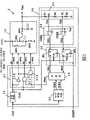
专利文献1公开了相关电源电路的一例。该电源电路1为供电泵型,如图1所示具有供电泵10和调节器20。从而,通过调节器20与供电泵10的输出电压相对应地跳过使供电泵10执行升压动作的时钟信号CLK1的脉冲,从供电泵10输出将电源电压VDD升压为所需电压值的电压(目标电压)作为Vout。关于供电泵10及调节器20的具体结构及动作的说明,在上述专利文献1中有详细记载,在此省略。
专利文献1:日本专利特开2005-20971号公报(图3、图4)Patent Document 1: Japanese Patent Laid-Open No. 2005-20971 (Fig. 3, Fig. 4)
上述电源电路1在轻负载时的升压动作,在时钟信号CLK1为“H”电平的期间,以取决于比较器22的动作速度的频率,由反复“L”电平和“H”电平的时钟信号CLK进行。基于该时钟信号CLK2的升压动作,根据Vout的输出电平,相对于时钟信号CLK1成为频率不定的动作。换言之,Vout的负载电流不固定,因此Vout的下降曲线的斜率也不固定。因此构成供电泵10的开关SW1~SW4的接通、断开周期也不固定。开关SW1~SW4中瞬时流过使升压电容器C1充电/放电的电流,因此需要使开关SW1~SW4为低阻抗。因此在驱动器IC的芯片布局内,开关SW1~SW4的尺寸非常大。由于开关SW1~SW4的尺寸很大,因此与开关SW1~SW4相邻的元件/布线数也很多。该大尺寸的开关SW1~SW4的频率不定动作成为噪声源,会导致引发驱动器IC内的相邻的逻辑电路等的误动作。The voltage boosting operation of the above-mentioned
发明内容Contents of the invention
在本发明的一个方面提供一种升压电源电路,其具有:供电泵,通过串并联切换将电容器与直流电源电压连接,通过电容器的充电电压使直流电源电压升压;和调节器,将上述供电泵的输出电压负反馈控制为目标电压。在该升压电源电路中,上述调节器检测出表示上述供电泵的输出电压与多个检测电压相比在各个检测电压以上或低于检测电压的信号,并根据上述检测信号的组合对上述串并联切换进行PWM控制。One aspect of the present invention provides a boosted power supply circuit, which has: a power supply pump, which connects a capacitor to a DC power supply voltage through series-parallel switching, and boosts the DC power supply voltage through the charging voltage of the capacitor; and a regulator, which connects the above-mentioned The output voltage of the power supply pump is controlled by negative feedback to the target voltage. In this step-up power supply circuit, the regulator detects a signal indicating that the output voltage of the power supply pump is higher than or lower than each detection voltage compared with a plurality of detection voltages, and adjusts the voltage of the string according to a combination of the detection signals. Parallel switching for PWM control.
在本发明的另一个方面提供一种升压方法。在该升压方法中准备升压电路,该升压电路具有供电泵和调节器,所述供电泵通过串并联切换将电容器与直流电压连接,通过电容器的充电电压使直流电压升压,所述调节器将上述供电泵的输出电压负反馈控制为目标电压。上述调节器检测出表示上述供电泵的输出电压与多个检测电压相比在各个检测电压以上或低于检测电压的信号,并根据上述检测信号的组合对上述串并联切换进行PWM控制。In another aspect of the present invention, a boosting method is provided. In this boosting method, a boosting circuit is prepared, the boosting circuit has a power supply pump that connects a capacitor to a DC voltage through series-parallel switching, and boosts the DC voltage by the charging voltage of the capacitor, and a regulator. The regulator negatively controls the output voltage of the power supply pump to a target voltage. The regulator detects a signal indicating that the output voltage of the power supply pump is higher than or lower than a plurality of detection voltages, and performs PWM control on the series-parallel switching based on a combination of the detection signals.
上述检测信号优选为二值信号的形式。The above detection signal is preferably in the form of a binary signal.
优选的是,上述供电泵的输出电压的检测通过将上述输出电压的分压电压与基准电压比较来进行,上述分压电压和基准电压的比较,是在进行比较的双方中的一方的值不同的多个电压和另一方的值单一的电压之间进行的。Preferably, the detection of the output voltage of the power supply pump is performed by comparing a divided voltage of the output voltage with a reference voltage, and the comparison between the divided voltage and the reference voltage is such that one of the two sides to be compared has a different value. between multiple voltages and a single voltage of value on the other.
优选的是,上述调节器具有:分频电路,生成升压时钟的2倍周期的分频时钟;分压电路,生成上述分压电压;比较电路,比较上述分压电压和基准电压,输出多个比较结果信号;和选择信号生成电路,与上述分频时钟的边沿同步地读入上述各比较结果信号的逻辑,并输出上述二值信号作为选择信号。Preferably, the above-mentioned regulator has: a frequency dividing circuit, which generates a frequency-divided clock with twice the period of the boost clock; a voltage dividing circuit, which generates the above-mentioned divided voltage; a comparison circuit, which compares the above-mentioned divided voltage and the reference voltage, and outputs more a comparison result signal; and a selection signal generating circuit, which reads in the logic of each of the comparison result signals synchronously with the edge of the above-mentioned frequency division clock, and outputs the above-mentioned binary signal as a selection signal.
进一步优选的是,上述调节器还具有:DUTY变换电路,输出与上述升压时钟的周期相同、占空比不同的多个时钟;选择器,根据上述选择信号选择上述多个时钟的某一个或“H”电平的逻辑来作为PWM信号;以及门电路,对上述分频时钟和PWM信号进行逻辑积运算,生成上述串并联切换的控制信号。Further preferably, the above-mentioned regulator also has: a DUTY conversion circuit, outputting a plurality of clocks with the same cycle as the above-mentioned boost clock and different duty ratios; a selector, selecting one or more of the above-mentioned multiple clocks according to the above-mentioned selection signal The logic of the "H" level is used as the PWM signal; and the gate circuit performs a logical product operation on the above-mentioned frequency-divided clock and the PWM signal to generate the above-mentioned series-parallel switching control signal.
优选的是,通过上述分压电路生成多个不同的分压电压,作为上述不同的多个电压,通过上述比较电路将上述多个不同的分压电压和单一的基准电压进行比较。Preferably, a plurality of different divided voltages are generated by the voltage dividing circuit, and the plurality of different divided voltages are compared with a single reference voltage by the comparison circuit as the plurality of different voltages.
发明效果Invention effect
根据本发明,控制供电泵的开关的控制信号总是与分频时钟的频率相同,因此在轻负载时也可以使所有的开关在确定的频率下持续动作,不会产生频率不定的高频动作,可以防止产生噪声。从而,在构成电源电路的半导体集成电路内的相邻的逻辑电路等中,可以防止产生因噪声引起的误动作。According to the present invention, the control signal for controlling the switch of the power supply pump is always the same as the frequency of the frequency-divided clock, so all the switches can continue to operate at a certain frequency when the load is light, and high-frequency operation with variable frequency will not occur , which prevents noise. Accordingly, it is possible to prevent malfunctions due to noise in adjacent logic circuits and the like within the semiconductor integrated circuit constituting the power supply circuit.
附图说明Description of drawings
图1是现有的供电泵型的一例的电源电路的电路图。FIG. 1 is a circuit diagram of an example of a conventional power supply pump type power supply circuit.
图2是本发明的第一实施方式的电源电路的电路图。FIG. 2 is a circuit diagram of a power supply circuit according to the first embodiment of the present invention.
图3是图2所示的电源电路中使用的选择器的电路图。FIG. 3 is a circuit diagram of a selector used in the power supply circuit shown in FIG. 2 .
图4是表示图1所示的电源电路的动作的信号波形图。FIG. 4 is a signal waveform diagram showing the operation of the power supply circuit shown in FIG. 1 .
图5是本发明的第二实施方式的电源电路的电路图。5 is a circuit diagram of a power supply circuit according to a second embodiment of the present invention.
图6是图5所示的电源电路中使用的选择器的电路图。FIG. 6 is a circuit diagram of a selector used in the power supply circuit shown in FIG. 5 .
图7是表示图5所示的电源电路的动作的信号波形图。FIG. 7 is a signal waveform diagram showing the operation of the power supply circuit shown in FIG. 5 .
具体实施方式Detailed ways
以下参照附图详细说明本发明的实施方式。图2是本发明的第一实施方式的电源电路2的电路图。电源电路2具有供电泵10和调节器30,使电源电压VDD为所需的升压电压(目标电压),并作为输出电压Vout提供到负载电路(未图示)。Embodiments of the present invention will be described in detail below with reference to the drawings. FIG. 2 is a circuit diagram of a power supply circuit 2 according to the first embodiment of the present invention. The power supply circuit 2 has a
供电泵10具有开关SW1~SW4、升压电容器C 1及平滑电容器C2。开关SW1~SW4由来自调节器30的控制信号S1~S4分别控制。通过开关SW1、SW2向升压电容器C1施加电源电压VDD而进行充电。通过开关SW3向被充电的升压电容器C1的低电位侧施加电源电压VDD,通过升压电容器C1的充电电压使电源电压VDD升压。通过开关SW4向平滑电容器C2施加升压电压而使升压电压平滑化,并且作为输出电压Vout提供到负载电路。另外,电源电路2是在半导体集成电路(即IC芯片)内与其他功能块一起构成,但升压电容器C1及平滑电容器C2是作为IC芯片的外部组件进行连接。The
调节器30具有分频电路31、DUTY(占空比)变换电路32、分压电路33、比较电路34、选择信号生成电路35、选择器36及门电路37,通过对输出电压Vout进行负反馈并控制供电泵,而将输出电压Vout调节为目标电压。The
分频电路31将来自未图示的振荡器的升压时钟CLK(占空比50%)分频为2倍周期的时钟(分频时钟)CLK1,并输出到选择信号生成电路35及门电路37。The frequency dividing
DUTY变换电路32生成与升压时钟CLK周期相同但占空比不同的时钟CLK2、CLK3,并输出到选择器36。时钟CLK2、CLK3的占空比被设定为CLK2>CLK3。时钟CLK3用于接近无负载的轻负载时的供电泵10的开关控制,时钟CLK3的占空比被设定为能够以可以将输出电压Vout调节为目标电压的最小脉冲宽度(最小占空比)进行开关控制,详细情况在下文说明。此外,时钟CLK2用于中负载时的供电泵10的开关控制,时钟CLK2的占空比被设定为能够以小于占空比50%并大于最小占空比的预定的占空比进行开关控制。The
分压电路33,通过电阻R1、R2、R3对来自供电泵10的输出电压Vout进行分压,将其分压电压Vd1、Vd2从分压点P1、P2输出到比较电路34。The
比较电路34具备具有迟滞特性的比较器COM1、COM2,将分压电压Vd1、Vd2与基准电压Vref比较,并将比较结果CPS1、CPS2输出到选择信号生成电路35。比较器COM1向反转输入端施加分压电压Vd1,向非反转输入端施加基准电压Vref。比较器COM2向反转输入端施加分压电压Vd2,向非反转输入端施加基准电压Vref。比较器COM1、COM2在分压电压Vd1、Vd2比基准电压Vref低时输出“H”电平的逻辑比较结果CPS1、CPS2,在分压电压Vd1、Vd2比基准电压Vref高时输出“L”电平的逻辑比较结果CPS1、CPS2。分压电压Vd1、Vd2用下式表示。The
Vd1=Vout×(R2+R3)/(R1+R2+R3)Vd1=Vout×(R2+R3)/(R1+R2+R3)
Vd2=Vout×R3/(R1+R2+R3)Vd2=Vout×R3/(R1+R2+R3)
Vout上升时比较器COM1、COM2的检测电压V(COM1)、V(COM2)用下式表示。When Vout rises, the detection voltages V(COM1) and V(COM2) of the comparators COM1 and COM2 are represented by the following equations.
V(COM1)=Vref×{1+R1/(R2+R3)}V(COM1)=Vref×{1+R1/(R2+R3)}
V(COM2)=Vref×{1+(R 1+R2)/R3}V(COM2)=Vref×{1+(
在此,检测电压V(COM2)被设定为输出电压Vout的升压目标电压。例如,设目标电压为5.5V时,如果Vref=2.75V,则设定为R1+R2=R3即可。此时如果设定为R1=R2,则检测电压V(COM1)=3.67V。即,V(COM2)=目标电压=5.5V>检测电压V(COM1)=3.67V。Here, the detection voltage V(COM2) is set as the boost target voltage of the output voltage Vout. For example, when the target voltage is 5.5V, if Vref=2.75V, then R1+R2=R3 may be set. At this time, if R1=R2 is set, the detection voltage V(COM1)=3.67V. That is, V(COM2)=target voltage=5.5V>detection voltage V(COM1)=3.67V.
选择信号生成电路35具有D型触发器(以下称为D触发器)FF1、FF2,根据比较结果CPS1、CPS2将选择信号SEL1、SEL2输出到选择器36。D触发器FF1、FF2在数据端子D输入比较结果CPS1、CPS2,在时钟端子CK输入时钟信号CLK1,在复位端子R输入复位信号RESET,从输出端子Q输出选择信号SEL1、SEL2。D触发器FF1、FF2在复位信号RESET的逻辑为“L”电平时被复位,输出端子Q的逻辑成为“L”电平。此外,D触发器FF1、FF2在复位信号RESET的逻辑为“H”电平时,与时钟CLK1的下降沿同步地读入数据端子D的逻辑、即比较结果CPS1、CPS2的逻辑,输出端子Q的逻辑成为其读入电平。Selection
选择器36如图3所示,具有OR电路361、363和AND电路362,根据选择信号SEL1、SEL2选择“H”电平的逻辑及时钟CLK2、CLK3中的一个,并作为PWM信号输出到门电路37。选择信号SEL2和时钟CLK3被二输入到OR电路361,进行逻辑和(“或”)运算。OR电路361的输出与时钟CLK2被二输入到AND电路362,进行逻辑积(“与”)运算。AND电路362的输出与选择信号SEL1被二输入到OR电路363,进行逻辑和运算。OR电路363的输出被输出到门电路37。As shown in FIG. 3, the
(SEL1,SEL2)=(H,H)时,输出“H”电平的逻辑。When (SEL1, SEL2) = (H, H), output "H" level logic.
(SEL1,SEL2)=(L,H)时,输出CLK2。When (SEL1, SEL2) = (L, H), CLK2 is output.
(SEL1,SEL2)=(L,L)时,输出CLK3。When (SEL1, SEL2) = (L, L), CLK3 is output.
门电路37具有AND电路371、372和NOT电路373,对时钟CLK1和PMW信号进行逻辑处理,将控制信号S1~S4输出到供电泵10。AND电路371将时钟信号CLK1与PWM信号进行逻辑积运算,并作为控制信号S1输出。AND电路372将时钟信号CLK1经由NOT电路373与PWM信号进行逻辑积运算,并作为控制信号S4输出。此外,时钟信号CLK1直接作为控制信号S2输出,并且经由NOT电路373作为控制信号S3输出。
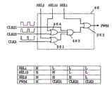
参照图4说明上述结构的电源电路2的动作。在电源电路2的动作状态(时刻t1~t4)中,向电源电路2提供电源电压VDD、基准电压Vref及复位信号RESET(未图示),并且如图4(c)所示以周期T1提供升压时钟CLK,如图4(b)所示从电源电路2向负载电路提供输出电压Vout。The operation of the power supply circuit 2 configured as described above will be described with reference to FIG. 4 . In the operating state of the power supply circuit 2 (time t1 to t4), the power supply voltage VDD, the reference voltage Vref and the reset signal RESET (not shown) are supplied to the power supply circuit 2, and are supplied in a cycle T1 as shown in FIG. 4(c). The boost clock CLK supplies the output voltage Vout from the power supply circuit 2 to the load circuit as shown in FIG. 4( b ).
输出电压Vout通过分压电路33分压,并作为分压电压Vd1、Vd2从分压电路33输出到比较电路34。在比较电路34中,通过比较器COM1、COM2将分压电压Vd1、Vd2与基准电压Vref比较,并作为后述的与输出电压Vout的值对应的比较结果CPS1、CPS2如图4(g)、(i)所示输出。比较器COM1、COM2的检测电压V(COM1)、V(COM2)因比较器COM1、COM2的迟滞特性,而如图4(b)所示存在点线所示的上限和短划线所示的下限的迟滞宽度。因此,检测电压V(COM1)、V(COM2)在输出电压Vout上升时通过点线所示的上限检测,在输出电压Vout下降时通过短划线所示的下限检测。The output voltage Vout is divided by the
升压时钟CLK被输入到分频电路并进行二分频,并如图4(d)所示从分频电路31作为周期2T1的时钟CLK1输出。此外,升压时钟CLK被输入到DUTY变换电路32,变换占空比,并如图4(e)、(f)所示从DUTY变换电路32作为时钟CLK2、CLK3输出。The boosted clock CLK is input to the frequency dividing circuit and divided by two, and is output from the
来自分频电路31的时钟CLK1被输入到门电路37。在门电路37中,时钟CLK1如图4(m)所示直接作为控制信号S2输出,并且如图4(n)所示经由NOT电路373将时钟CLK1反转后的时钟CLK1B作为控制信号S3输出。此外,时钟CLK1在AND电路371中、以及经由NOT电路373在AND电路372中,与后述的与输出电压Vout的值对应的PWM信号一起被二输入,并进行逻辑积运算。AND电路371、372的输出分别如图4(l)、(o)所示作为控制信号S1、S4输出。The clock CLK1 from the
此外,来自分频电路31的时钟CLK1也被输入到选择信号生成电路35中。在选择信号生成电路35中,时钟CLK1被输入到D触发器FF1、FF2的时钟端子CK中。在D触发器FF1、FF2中,与时钟CLK1的下降沿同步地,读入数据端子D的逻辑、即后述的与输出电压Vout的值对应的CPS1、CPS2的逻辑,输出端子Q的逻辑成为其读入电平,并如图4(h)、(j)所示作为选择信号SEL1、SEL2输出。另外,D触发器FF1、FF2在时刻t1以前的电源电路2开始动作时,通过复位信号RESET的“L”电平的逻辑而被复位,之后固定为“H”电平的逻辑(未图示)。In addition, the clock CLK1 from the
来自DUTY变换电路32的时钟CLK2、CLK3被输入到选择器36。在选择器36中,根据后述的与输出电压Vout的值对应的选择信号SEL1、SEL2,选择时钟CLK2、CLK3中的某一个或“H”电平的逻辑,并如图4(k)所示作为PWM信号输出。Clocks CLK2 and CLK3 from the
来自门电路37的控制信号S1~S4被输入到供电泵10。在供电泵10中,控制信号S1通过“H”电平的逻辑而接通控制开关SW1,控制信号S2通过“H”电平的逻辑而接通控制开关SW2,控制信号S3通过“H”电平的逻辑而接通控制开关SW3,控制信号S4通过“H”电平的逻辑而接通控制开关SW4。在开关SW1、SW2接通、开关SW3、SW4断开时,升压电容器C1由电源电压VDD充电。在开关SW1、SW2断开、开关SW3、SW4接通时,电源电压VDD通过升压电容器C1的充电电压而升压,升压电压通过平滑电容器C2而平滑化,并从供电泵10输出。Control signals S1 to S4 from
以下,对于生成与输出电压Vout的值对应的控制信号S1、S4的动作,按照负载电路的负载电平、即负载电流I0的电平划分并进行说明。如图4(a)所示,以负载电平随时间变为轻负载→中负载→重负载的情况为例进行说明。Hereinafter, the operation of generating the control signals S1 and S4 corresponding to the value of the output voltage Vout will be divided and described according to the load level of the load circuit, that is, the level of the load currentI0 . As shown in FIG. 4( a ), a case where the load level changes over time from light load→medium load→heavy load will be described as an example.
(1)轻负载状态:负载电流I0=小(时刻t1~t2)(1) Light load state: load current I0 = small (time t1~t2)
在时刻t1~t2中,输出电压Vout如图4(b)所示,为比较器COM2的检测电压V(COM2)的下限以上(Vref≤Vd2),比较结果CPS1、CPS2如图4(g)、(i)所示为“L”电平的逻辑。因此选择信号SEL1、SEL2如图4(h)、(j)所示仍为“L”电平的逻辑。其结果,作为PWM信号,如图4(k)所示选择时钟CLK3。从而如图4(1)所示,控制信号S 1将时钟CLK3和时钟CLK1进行逻辑积运算,成为上升沿及周期与时钟CLK1相同、且占空比为时钟CLK3的一半的信号。此外如图4(o)所示,控制信号S4将时钟CLK3和时钟CLK1B进行逻辑积运算,成为上升沿及周期与时钟CLK1B相同、且占空比为时钟CLK3的一半的信号。At time t1~t2, the output voltage Vout is above the lower limit of the detection voltage V(COM2) of the comparator COM2 (Vref≤Vd2), as shown in Figure 4(b), and the comparison results CPS1 and CPS2 are shown in Figure 4(g) , (i) shows the logic of "L" level. Therefore, the selection signals SEL1 and SEL2 are still logic at "L" level as shown in Fig. 4(h) and (j). As a result, the clock CLK3 is selected as the PWM signal as shown in FIG. 4( k ). Thus, as shown in FIG. 4(1), the control signal S1 performs a logical product operation on the clock CLK3 and the clock CLK1, and becomes a signal with the same rising edge and cycle as the clock CLK1, and a duty cycle that is half of the clock CLK3. In addition, as shown in FIG. 4( o ), the control signal S4 performs a logical product operation on the clock CLK3 and the clock CLK1B, and becomes a signal with the same rising edge and cycle as the clock CLK1B, and a duty ratio half of the clock CLK3.
(2)中负载:负载电流I0=中(时刻t2~t3)(2) Medium load: load current I0 = medium (time t2~t3)
在变为时刻t21时,如图4(b)所示,输出电压Vout为比较器COM1的检测电压V(COM1)的下限以上(Vref≤Vd1),且低于比较器COM2的检测电压V(COM2)的下限(Vref>Vd2)。此时如图4(i)所示,比较结果CPS2成为“H”电平的逻辑。比较结果CPS1如图4(g)所示,仍为“L”电平的逻辑。在时刻t21~t3中,输出电压Vout为比较器COM1的检测电压V(COM1)的下限以上(Vref≤Vd1),且低于比较器COM2的检测电压V(COM2)的上限(Vref>Vd2)。此时如图4(g)所示比较结果CPS1仍为“L”电平的逻辑。如图4(i)所示比较结果CPS2仍为“H”电平的逻辑。因此如图4(j)所示,选择信号SEL2在时刻t22与时钟CLK1的下降沿同步地变为“H”电平的逻辑,且在时刻t22~t3中持续为“H”电平的逻辑。如图4(h)所示,选择信号SEL1在时刻t22~t3中仍为“L”电平的逻辑。其结果,在时刻t22~t3中,如图4(k)所示作为PWM信号选择时钟CLK2。从而如图4(l)所示,控制信号S1将时钟CLK2和时钟CLK1进行逻辑积运算,成为上升沿及周期与时钟CLK1相同、且占空比为时钟CLK2的一半的信号。此外如图4(o)所示,控制信号S4将时钟CLK2和时钟CLK1B进行逻辑积运算,成为上升沿及周期与时钟CLK1B相同、且占空比为时钟CLK2的一半的信号。At time t21, as shown in FIG. 4(b), the output voltage Vout is equal to or higher than the lower limit of the detection voltage V(COM1) of the comparator COM1 (Vref≦Vd1), and is lower than the detection voltage V(COM1) of the comparator COM2. COM2) lower limit (Vref>Vd2). At this time, as shown in FIG. 4(i), the logic of the comparison result CPS2 becomes "H" level. The comparison result CPS1 is shown in Fig. 4(g), which is still logic of "L" level. From time t21 to t3, the output voltage Vout is equal to or higher than the lower limit of the detection voltage V(COM1) of the comparator COM1 (Vref≤Vd1), and is lower than the upper limit of the detection voltage V(COM2) of the comparator COM2 (Vref>Vd2) . At this time, as shown in FIG. 4(g), the comparison result CPS1 is still logic of "L" level. As shown in Fig. 4(i), the logic of the comparison result CPS2 is still "H" level. Therefore, as shown in FIG. 4(j), the selection signal SEL2 becomes "H" level logic in synchronization with the falling edge of the clock CLK1 at time t22, and continues to be "H" level logic at time t22 to t3. . As shown in FIG. 4( h ), the selection signal SEL1 remains logic at the "L" level at times t22 to t3. As a result, at times t22 to t3, the clock CLK2 is selected as the PWM signal as shown in FIG. 4( k ). Therefore, as shown in FIG. 4(l), the control signal S1 performs a logical product operation on the clock CLK2 and the clock CLK1, and becomes a signal with the same rising edge and cycle as the clock CLK1, and a duty cycle that is half of the clock CLK2. In addition, as shown in FIG. 4( o ), the control signal S4 performs a logical product operation on the clock CLK2 and the clock CLK1B, and becomes a signal with the same rising edge and cycle as the clock CLK1B, and a duty ratio half of the clock CLK2.
(3)重负载:负载电流I0=大(时刻t3~t4)(3) Heavy load: load current I0 = large (time t3~t4)
在变为时刻t31时,如图4(b)所示,输出电压Vout低于比较器COM1的检测电压V(COM1)的下限(Vref>Vd1)。此时如图4(g)所示比较结果CPS1成为“H”电平的逻辑。如图4(i)所示比较结果CPS2仍为“H”电平的逻辑。在时刻t31~t4中,输出电压Vout低于比较器COM1的检测电压V(COM1)的上限(Vref>Vd1)。此时如图4(g)、(i)所示,比较结果CPS1、CPS2仍为“H”电平的逻辑。因此如图4(h)所示,选择信号SEL1在时刻t32与时钟CLK1的下降沿同步地变为“H”电平的逻辑,且在时刻t32~t4中持续为“H”电平的逻辑。如图4(j)所示,选择信号SEL2在时刻t32~t4中仍为“H”电平的逻辑。其结果,在时刻t32~t4中,如图4(k)所示作为PWM信号选择“H”电平的逻辑。从而如图4(l)所示,时钟CLK1成为控制信号S1。此外如图4(o)所示,时钟CLK1B成为控制信号S4。At time t31, as shown in FIG. 4(b), the output voltage Vout falls below the lower limit of the detection voltage V(COM1) of the comparator COM1 (Vref>Vd1). At this time, the comparison result CPS1 becomes the logic of "H" level as shown in FIG. 4(g). As shown in Fig. 4(i), the logic of the comparison result CPS2 is still "H" level. From time t31 to t4, the output voltage Vout is lower than the upper limit of the detection voltage V(COM1) of the comparator COM1 (Vref>Vd1). At this time, as shown in Fig. 4(g) and (i), the comparison results CPS1 and CPS2 are still logic of "H" level. Therefore, as shown in FIG. 4(h), the selection signal SEL1 becomes "H" level logic in synchronization with the falling edge of clock CLK1 at time t32, and continues to be "H" level logic at time t32~t4. . As shown in FIG. 4( j ), the selection signal SEL2 remains logic at the "H" level at times t32 to t4. As a result, at times t32 to t4, logic at "H" level is selected as the PWM signal as shown in FIG. 4(k). Thus, as shown in FIG. 4(l), the clock CLK1 becomes the control signal S1. Furthermore, as shown in FIG. 4( o ), the clock CLK1B becomes the control signal S4.
如上所述,电源电路2通过使供电泵10的开关控制对应于三种负载状态而为三种占空比的方式进行PWM控制。在升压时钟的2倍周期中,为重负载时,是50%的占空比;为接近无负载的轻负载时,是最小占空比;为中负载时,是小于50%且大于最小占空比的预定的占空比。因此不会进行频率不定的高频下的开关控制,不会产生噪声。As described above, the power supply circuit 2 performs PWM control so that the switching control of the
图5是本发明的第二实施方式的电源电路3的电路图。对与图2相同的构成要素标以相同的标记并省略其说明。电源电路3是在图2的电源电路2中将调节器30置换为调节器40。在调节器40中,进一步追加一个比较器以可以在比较器COM1的检测电压和比较器COM2的检测电压之间检测输出电压Vout,以两种占空比进行比较器COM1的检测电压和比较器COM2的检测电压之间的PWM控制。FIG. 5 is a circuit diagram of a
调节器40是在图2的调节器30中,将DUTY变换电路32、分压电路33、比较电路34、选择信号生成电路35及选择器36,置换为DUTY变换电路42、分压电路43、比较电路44、选择信号生成电路45及选择器46。The regulator 40 is in the
DUTY变换电路42是在图2的DUTY变换电路32中将时钟CLK2的输出,置换为与升压时钟CLK周期相同但占空比不同的时钟CLK21、CLK22的输出。时钟CLK21、CLK22的占空比被设定为CLK21>CLK22。时钟CLK21、CLK22与时钟CLK2同样地,用于中负载时的供电泵10的开关控制,时钟CLK21、CLK22的占空比被设定为能够以小于占空比50%并大于最小占空比的预定的占空比进行开关控制。The duty conversion circuit 42 replaces the output of the clock CLK2 in the
分压电路43是在图2的分压电路33中将电阻R2分割为电阻R21、R22,从电阻R21、R22的分压点P12输出分压电压Vd12。The voltage dividing circuit 43 divides the resistor R2 into the resistors R21 and R22 in the
比较电路44是在图2的比较电路34中进一步追加具有迟滞特性的比较器COM12,将分压点P12的分压电压Vd12与基准电压Vref比较。其比较结果CPS12被输出到选择信号生成电路45。比较器COM12向反转输入端施加分压电压Vd12,向非反转输入端施加基准电压Vref。比较器COM12在分压电压Vd12比基准电压Vref低时输出“H”电平的逻辑比较结果CPS12,在分压电压Vd12比基准电压Vref高时输出“L”电平的逻辑比较结果CPS12。分压电压Vd12用下式表示。The comparison circuit 44 is a comparator COM12 having a hysteresis characteristic added to the
Vd12=Vout×(R22+R3)/(R1+R21+R22+R3)Vd12=Vout×(R22+R3)/(R1+R21+R22+R3)
Vout上升时比较器COM12的检测电压V(COM12)用下式表示。The detection voltage V(COM12) of the comparator COM12 when Vout rises is represented by the following formula.
V(COM12)=Vref×{1+(R1+R21)/(R22+R3)}V(COM12)=Vref×{1+(R1+R21)/(R22+R3)}
在此,例如设定为R21=R22,则检测电压V(COM12)=4.4V。即,V(COM2)=目标电压=5.5V>V(COM12)=4.4V>V(COM1)=3.67V。Here, for example, if R21=R22 is set, the detection voltage V(COM12)=4.4V. That is, V(COM2)=target voltage=5.5V>V(COM12)=4.4V>V(COM1)=3.67V.
选择信号生成电路45是在图2的选择信号生成电路35中进一步追加D触发器FF12,根据比较结果CPS12将选择信号SEL12输出到选择器46。D触发器FF12在数据端子D输入比较结果CPS12,在时钟端子CK输入时钟信号CLK1,在复位端子R输入复位信号RESET,从输出端子Q输出选择信号SEL12。D触发器FF12与D触发器FF1、FF2同样地进行动作。The selection signal generation circuit 45 further adds a D flip-flop FF12 to the selection
选择器46如图6所示,在图3的选择器36中,将AND电路363置换为三输入的AND电路462,并进一步追加OR电路464。根据选择信号生成电路45的选择信号SEL1、SEL12、SEL2,选择逻辑的“H”电平及时钟CLK21、CLK22、CLK3中的一个,并作为PWM信号输出到门电路37。选择信号SEL12和时钟CLK22被二输入到OR电路464,进行逻辑和运算。OR电路361、464的输出与时钟CLK21被三输入到AND电路462,进行逻辑积运算。AND电路462的输出与选择信号SEL1被二输入到OR电路363,进行逻辑和运算。As shown in FIG. 6 , the
(SEL1,SEL12,SEL2)=(H,H,H)时,输出“H”电平的逻辑。When (SEL1, SEL12, SEL2) = (H, H, H), the logic to output "H" level.
(SEL1,SEL12,SEL2)=(L,H,H)时,输出CLK21。When (SEL1, SEL12, SEL2)=(L, H, H), CLK21 is output.
(SEL1,SEL12,SEL2)=(L,L,H)时,输出CLK22。When (SEL1, SEL12, SEL2)=(L, L, H), CLK22 is output.
(SEL1,SEL12,SEL2)=(L,L,L)时,输出CLK3。When (SEL1, SEL12, SEL2)=(L, L, L), CLK3 is output.
参照图7说明上述结构的电源电路3的动作。在电源电路3的动作状态(时刻t1~t5)中,关于与电源电路2相同结构的电路的动作,与电源电路2的动作相同,仅对不同的动作进行说明。The operation of the
将分压电压Vd12从分压电路43的分压点P12输出到比较电路44。在比较电路44中,通过比较器COM12将分压电压Vd12与基准电压Vref比较,并作为后述的与输出电压Vout的值对应的比较结果CPS12如图7(gi)所示输出。The divided voltage Vd12 is output from the divided voltage point P12 of the voltage divided circuit 43 to the comparison circuit 44 . In the comparison circuit 44, the divided voltage Vd12 is compared with the reference voltage Vref by the comparator COM12, and is output as a comparison result CPS12 corresponding to the value of the output voltage Vout described later as shown in FIG. 7(gi).
比较器COM12的检测电压V(COM12)因比较器COM12的迟滞特性,而如图7(b)所示存在点线所示的上限和短划线所示的下限的迟滞宽度,在输出电压Vout上升时通过点线所示的上限检测,在输出电压Vout下降时通过短划线所示的下限检测。Due to the hysteresis characteristics of the comparator COM12, the detection voltage V(COM12) of the comparator COM12 has a hysteresis width of an upper limit indicated by a dotted line and a lower limit indicated by a dashed line as shown in FIG. 7(b). When rising, the upper limit detection shown by the dotted line is used, and when the output voltage Vout falls, the lower limit detection shown by the dashed line is used.
如图7(e1)、(e2)所示从DUTY变换电路42作为时钟CLK21、CLK22输出。As shown in FIG. 7( e1 ), ( e2 ), it is output from the duty conversion circuit 42 as clocks CLK21 and CLK22 .
在选择信号生成电路45中,时钟CLK1被输入到D触发器FF12的时钟端子CK中。在D触发器FF12中,与时钟CLK1的下降沿同步地,读入数据端子D的逻辑、即后述的与输出电压Vout的值对应的CPS12的逻辑,输出端子Q的逻辑成为其读入电平,并如图7(hj)所示作为选择信号SEL12输出。另外,复位信号RESET下的动作与D触发器FF1、FF2相同。In the selection signal generating circuit 45 , the clock CLK1 is input to the clock terminal CK of the D flip-flop FF12 . In the D flip-flop FF12, in synchronization with the falling edge of the clock CLK1, the logic of the data terminal D, that is, the logic of the CPS12 corresponding to the value of the output voltage Vout described later is read, and the logic of the output terminal Q becomes its read voltage. level, and output as a selection signal SEL12 as shown in FIG. 7(hj). In addition, the operation under the reset signal RESET is the same as that of the D flip-flops FF1 and FF2.
来自DUTY变换电路42的时钟CLK21、CLK22被输入到选择器46。在选择器46中,根据后述的与输出电压Vout的值对应的选择信号SEL1、SEL12、SEL2,选择时钟CLK21、CLK22、CLK3中的某一个或“H”电平的逻辑,并如图7(k)所示作为PWM信号输出。Clocks CLK21 and CLK22 from the duty conversion circuit 42 are input to the
以下,对于生成与输出电压Vout的值对应的控制信号S1、S4的动作,按照负载电路的负载电平、即负载电流I0的电平划分并进行说明。如图7(a)所示,以负载电平随时间变为轻负载→中负载→重负载的情况为例进行说明。Hereinafter, the operation of generating the control signals S1 and S4 corresponding to the value of the output voltage Vout will be divided and described according to the load level of the load circuit, that is, the level of the load currentI0 . As shown in FIG. 7( a ), a case where the load level changes over time from light load→medium load→heavy load will be described as an example.
(1)轻负载状态:负载电流I0=小(时刻t1~t2)(1) Light load state: load current I0 = small (time t1~t2)
在时刻t1~t2中,输出电压Vout如图7(b)所示,为比较器COM2的检测电压V(COM2)的下限以上(Vref≤Vd2),比较结果CPSl、CPSl2、CPS2如图7(g)、(gi)、(i)所示为“L”电平的逻辑。因此选择信号SELl、SELl2、SEL2如图7(h)、(hj)、(j)所示仍为“L”电平的逻辑。其结果,作为PWM信号,如图7(k)所示选择时钟CLK3。从而如图7(l)、(o)所示,控制信号S1、S4为与电源电路2相同的占空比的信号。In the time t1~t2, the output voltage Vout as shown in Figure 7(b), is above the lower limit of the detection voltage V(COM2) of the comparator COM2 (Vref≤Vd2), and the comparison results CPS1, CPS12, CPS2 are shown in Figure 7 ( g), (gi), and (i) show logic at "L" level. Therefore, the selection signals SEL1, SEL12, and SEL2 are still logic of "L" level as shown in Fig. 7(h), (hj), and (j). As a result, the clock CLK3 is selected as the PWM signal as shown in FIG. 7(k). Therefore, as shown in FIG. 7( l) and (o), the control signals S1 and S4 are signals of the same duty ratio as that of the power supply circuit 2 .
(2)中小负载:负载电流I0=中小(时刻t2~t3)(2) Medium and small load: load current I0 = medium and small (time t2~t3)
在变为时刻t21时,如图7(b)所示,输出电压Vout为比较器COMl 2的检测电压V(COMl2)的下限以上(Vref≤Vdl2),且低于比较器COM2的检测电压V(COM2)的下限(Vref>Vd2)。此时如图7(i)所示,比较结果CPS2成为“H”电平的逻辑。比较结果CPSl、CPSl2如图7(g)、(gi)所示,仍为“L”电平的逻辑。在时刻t21~t3中,输出电压Vout为比较器COMl2的检测电压V(COMl2)的下限以上(Vref≤Vdl2),且低于比较器COM2的检测电压V(COM2)的上限(Vref>Vd2)。此时如图7(g)、(gi)所示比较结果CPSl、CPS 12仍为“L”电平的逻辑。如图7(i)所示比较结果CPS2仍为“H”电平的逻辑。因此如图7(j)所示,选择信号SEL2在时刻t22与时钟CLKl的下降沿同步地变为“H”电平的逻辑,且在时刻t22~t3中持续为“H”电平的逻辑。如图7(h)、(hj)所示,选择信号SELl、SELl2在时刻t22~t3中仍为“L”电平的逻辑。其结果,在时刻t22~t3中,如图7(k)所示作为PWM信号选择时钟CLK22。从而控制信号S1、S4成为图7(l)、(o)所示的占空比的信号。At time t21, as shown in FIG. 7(b), the output voltage Vout is above the lower limit of the detection voltage V(COM12) of the comparator COM12 (Vref≤Vd12), and is lower than the detection voltage V of the comparator COM2. The lower limit of (COM2) (Vref>Vd2). At this time, as shown in FIG. 7(i), the logic of the comparison result CPS2 becomes "H" level. Comparison results CPSl, CPSl2 shown in Figure 7 (g), (gi) is still "L" level logic. During time t21-t3, the output voltage Vout is above the lower limit of the detection voltage V(COM12) of the comparator COM12 (Vref≤Vdl2), and is lower than the upper limit of the detection voltage V(COM2) of the comparator COM2 (Vref>Vd2) . Now the comparison results CPS1, CPS12 shown in Figure 7 (g), (gi) are still the logic of "L" level. As shown in FIG. 7(i), the logic of the comparison result CPS2 is still "H" level. Therefore, as shown in FIG. 7(j), the selection signal SEL2 becomes the logic of "H" level synchronously with the falling edge of the clock CLK1 at time t22, and continues to be the logic of "H" level from time t22 to t3. . As shown in FIG. 7(h), (hj), the selection signal SEL1, SEL12 is still logic of "L" level in time t22-t3. As a result, at times t22 to t3, the clock CLK22 is selected as the PWM signal as shown in FIG. 7( k ). Therefore, the control signals S1 and S4 become signals of the duty ratios shown in FIGS. 7( l) and (o).
(3)中大负载:负载电流I0=中大(时刻t3~t4)(3) Medium and large load: load current I0 = medium and large (time t3~t4)
在变为时刻t31时,如图7(b)所示,输出电压Vout为比较器COMl的检测电压V(COMl)的下限以上(Vref≤Vdl),且低于比较器COMl2的检测电压V(COM2)的下限(Vref>Vdl2)。此时如图7(gi)所示,比较结果CPSl2成为“H”电平的逻辑。比较结果CPSl如图7(g)所示,仍为“L”电平的逻辑。比较结果CPS2如图7(i)所示,仍为“H”电平的逻辑。在时刻t31~t4中,输出电压Vout为比较器COMl的检测电压V(COMl)的下限以上(Vref≤Vdl),且低于比较器COMl2的检测电压V(COM12)的上限(Vref>Vd12)。此时如图7(g)所示比较结果CPS1仍为“L”电平的逻辑。如图7(i)所示比较结果CPS2仍为“H”电平的逻辑。因此如图7(hj)所示,选择信号SEL12在时刻t32与时钟CLK1的下降沿同步地变为“H”电平的逻辑,且在时刻t32~t4中持续为“H”电平的逻辑。如图7(h)所示,选择信号SEL1在时刻t32~t4中仍为“L”电平的逻辑。如图7(hj)所示,选择信号SEL12在时刻t32~t4中仍为“H”电平的逻辑。其结果,在时刻t32~t4中,如图7(k)所示作为PWM信号选择时钟CLK22。从而控制信号S1、S4成为图7(l)、(o)所示的占空比的信号。At time t31, as shown in FIG. 7(b), the output voltage Vout is above the lower limit of the detection voltage V(COM1) of the comparator COM1 (Vref≤Vdl), and is lower than the detection voltage V( COM2) lower limit (Vref>Vdl2). At this time, as shown in FIG. 7(gi), the logic of the comparison result CPSl2 becomes "H" level. The comparison result CPS1 is shown in Fig. 7(g), which is still logic of "L" level. The comparison result CPS2 is still logic of "H" level as shown in Fig. 7(i). During time t31-t4, the output voltage Vout is above the lower limit of the detection voltage V(COM1) of the comparator COM1 (Vref≤Vdl), and is lower than the upper limit of the detection voltage V(COM12) of the comparator COM12 (Vref>Vd12) . At this time, as shown in FIG. 7(g), the comparison result CPS1 is still logic of "L" level. As shown in FIG. 7(i), the logic of the comparison result CPS2 is still "H" level. Therefore, as shown in FIG. 7(hj), the selection signal SEL12 becomes logic of "H" level synchronously with the falling edge of clock CLK1 at time t32, and continues to be logic of "H" level from time t32 to t4. . As shown in FIG. 7( h ), the selection signal SEL1 remains logic at the "L" level at times t32 to t4. As shown in FIG. 7( hj ), the selection signal SEL12 remains logic at the "H" level at times t32 to t4. As a result, at times t32 to t4, the clock CLK22 is selected as the PWM signal as shown in FIG. 7( k ). Therefore, the control signals S1 and S4 become signals of the duty ratios shown in FIGS. 7( l) and (o).
(4)重负载:负载电流I0=大(时刻t4~t5)(4) Heavy load: load current I0 = large (time t4~t5)
在变为时刻t41时,如图7(b)所示,输出电压Vout低于比较器COM1的检测电压V(COM1)的下限(Vref>Vd1)。此时如图7(g)所示比较结果CPS1成为“H”电平的逻辑。如图7(i)、(gi)所示比较结果CPS2、CPS12仍为“H”电平的逻辑。在时刻t41~t5中,输出电压Vout低于比较器COM1的检测电压V(COM1)的上限(Vref>Vd1)。此时如图7(i)、(gi)所示,比较结果CPS2、CPS12仍为“H”电平的逻辑。因此如图7(h)所示,选择信号SEL1在时刻t42与时钟CLK1的下降沿同步地变为“H”电平的逻辑,且在时刻t42~t5中持续为“H”电平的逻辑。如图7(h)、(hj)所示,选择信号SEL2、SEL12在时刻t42~t5中仍为“H”电平的逻辑。其结果,在时刻t42~t5中,如图7(k)所示作为PWM信号选择“H”电平的逻辑。从而如图7(l)所示,时钟CLK1成为控制信号S1。此外如图7(o)所示,时钟CLK1B成为控制信号S4。At time t41, as shown in FIG. 7(b), the output voltage Vout falls below the lower limit of the detection voltage V(COM1) of the comparator COM1 (Vref>Vd1). At this time, the comparison result CPS1 becomes the logic of "H" level as shown in FIG. 7(g). The comparison results CPS2 and CPS12 as shown in Fig. 7(i) and (gi) are logic of "H" level. From time t41 to t5, the output voltage Vout is lower than the upper limit of the detection voltage V(COM1) of the comparator COM1 (Vref>Vd1). At this time, as shown in Fig. 7(i) and (gi), the comparison results CPS2 and CPS12 are still logic of "H" level. Therefore, as shown in FIG. 7(h), the selection signal SEL1 becomes "H" level logic in synchronization with the falling edge of the clock CLK1 at time t42, and continues to be "H" level logic at time t42 to t5. . As shown in (h) and (hj) of FIG. 7 , the selection signals SEL2 and SEL12 are still in the logic of "H" level at times t42 to t5. As a result, at times t42 to t5, logic at "H" level is selected as the PWM signal as shown in FIG. 7(k). Thus, as shown in FIG. 7(l), the clock CLK1 becomes the control signal S1. Furthermore, as shown in FIG. 7( o ), the clock CLK1B becomes the control signal S4.
如上所述,电源电路3通过两种占空比进行比较器COM1的检测电压和比较器COM2的检测电压之间的PWM控制。从而,除了电源电路2的效果之外,与电源电路2的情况相比可以将输出电压Vout的波动抑制得较低。As described above, the
另外,在上述第一及第二实施方式中,以将电压值不同的多个分压电压与单一的基准电压比较的结构为例进行了说明,但也可以是将单一的分压电压与多个基准电压比较的结构。此外,在第二实施方式中,以通过两种占空比进行比较器COM1的检测电压和比较器COM2的检测电压之间的PWM控制的情况为例进行了说明,但也可以通过三种以上的占空比进行。In addition, in the above-mentioned first and second embodiments, a structure in which a plurality of divided voltages having different voltage values are compared with a single reference voltage has been described as an example, but a single divided voltage may be compared with a plurality of voltages. The structure of a reference voltage comparison. In addition, in the second embodiment, the case where the PWM control between the detection voltage of the comparator COM1 and the detection voltage of the comparator COM2 is performed by two kinds of duty ratios was described as an example, but it is also possible to use three or more duty ratios. The duty cycle is performed.
Claims (8)
Translated fromChineseApplications Claiming Priority (3)
| Application Number | Priority Date | Filing Date | Title |
|---|---|---|---|
| JP2007-176123 | 2007-07-04 | ||
| JP2007176123AJP5154152B2 (en) | 2007-07-04 | 2007-07-04 | Boost power supply circuit |
| JP2007176123 | 2007-07-04 |
Publications (2)
| Publication Number | Publication Date |
|---|---|
| CN101383558A CN101383558A (en) | 2009-03-11 |
| CN101383558Btrue CN101383558B (en) | 2012-10-10 |
Family
ID=40357891
Family Applications (1)
| Application Number | Title | Priority Date | Filing Date |
|---|---|---|---|
| CN200810128306XAExpired - Fee RelatedCN101383558B (en) | 2007-07-04 | 2008-07-04 | Step-up power supply circuit and stepping-up method |
Country Status (3)
| Country | Link |
|---|---|
| US (1) | US7741899B2 (en) |
| JP (1) | JP5154152B2 (en) |
| CN (1) | CN101383558B (en) |
Families Citing this family (33)
| Publication number | Priority date | Publication date | Assignee | Title |
|---|---|---|---|---|
| JP5011182B2 (en)* | 2008-03-24 | 2012-08-29 | ルネサスエレクトロニクス株式会社 | Charge pump circuit |
| US20100001788A1 (en)* | 2008-07-06 | 2010-01-07 | Barth Jr John E | System to evaluate charge pump outputs and associated methods |
| CN101771340B (en)* | 2008-12-31 | 2012-10-31 | 中芯国际集成电路制造(上海)有限公司 | Charge pump |
| US8502587B2 (en)* | 2009-12-22 | 2013-08-06 | Fairchild Semiconductor Corporation | Fast recovery voltage regulator |
| US8134403B2 (en)* | 2009-12-22 | 2012-03-13 | Fairchild Semiconductor Corporation | Reduced current charge pump |
| CN101841229B (en)* | 2010-02-10 | 2012-09-19 | Bcd半导体制造有限公司 | A Clock External Synchronization Device for Switching Power Supply |
| KR101102969B1 (en)* | 2010-02-25 | 2012-01-10 | 매그나칩 반도체 유한회사 | Semiconductor devices |
| KR101852065B1 (en)* | 2011-02-17 | 2018-06-07 | 삼성전자주식회사 | Power supply apparatus for latch-up free charge pump and method there-of |
| JP5697621B2 (en)* | 2012-02-29 | 2015-04-08 | 株式会社東芝 | DC-DC converter and audio output device |
| JP2013258895A (en)* | 2012-05-18 | 2013-12-26 | Semiconductor Energy Lab Co Ltd | Semiconductor device and method for driving the same |
| EP2912835A4 (en) | 2012-10-23 | 2016-10-19 | Bounce Imaging Inc | REMOTE SURVEILLANCE SENSOR APPARATUS |
| CN102946193B (en)* | 2012-10-26 | 2015-02-25 | 华为技术有限公司 | Method for increasing comparison speed of comparator circuit and comparator circuit |
| CN103106882A (en)* | 2013-01-23 | 2013-05-15 | 深圳市华星光电技术有限公司 | Clock control circuit, driving circuit and liquid crystal display device |
| TWI508420B (en) | 2013-03-15 | 2015-11-11 | Silicon Motion Inc | Switching-capacitor regulator with charge injection mode for high loading current |
| US9553519B2 (en)* | 2013-06-04 | 2017-01-24 | Intel Corporation | Small form factor voltage adapters and devices, platforms, and techniques for managing power boosts |
| US9177708B2 (en) | 2013-06-14 | 2015-11-03 | Varian Semiconductor Equipment Associates, Inc. | Annular cooling fluid passage for magnets |
| US9246382B2 (en)* | 2013-08-08 | 2016-01-26 | Micron Technology, Inc. | Charge pump including supply voltage-based control signal level |
| CN103683908B (en)* | 2013-12-19 | 2015-11-25 | 矽力杰半导体技术(杭州)有限公司 | Switching power source control circuit, Switching Power Supply and control method thereof |
| CN104518663B (en)* | 2014-07-18 | 2017-03-29 | 上海华虹宏力半导体制造有限公司 | Negative pressure charge pump feedback circuit |
| WO2016131010A1 (en) | 2015-02-13 | 2016-08-18 | Apple Inc. | Charge pump having ac and dc outputs for touch panel bootstrapping and substrate biasing |
| KR102405182B1 (en)* | 2015-08-06 | 2022-06-08 | 삼성디스플레이 주식회사 | Boosting voltage generator and display apparatus including the same |
| CN106253665B (en)* | 2016-08-29 | 2019-06-25 | 深圳市华星光电技术有限公司 | Increase the charge pump of buck amplitude |
| TWI607623B (en)* | 2016-10-07 | 2017-12-01 | 新唐科技股份有限公司 | Switched-capacitor dc-dc power converter and control method thereof |
| CN106788398B (en)* | 2016-12-06 | 2020-06-02 | 矽力杰半导体技术(杭州)有限公司 | Clock frequency dividing circuit, control circuit and power management integrated circuit |
| US11190182B2 (en)* | 2017-02-13 | 2021-11-30 | Skyworks Solutions, Inc. | Control circuitry for silicon-on-insulator chip |
| US10401661B2 (en)* | 2017-06-22 | 2019-09-03 | Shenzhen China Star Optoelectronics Semiconductor Display Technology Co., Ltd. | Method for manufacturing metal wire and array substrate using the same |
| US11637506B2 (en)* | 2018-01-10 | 2023-04-25 | Polaris Industries Inc. | Low loss shunt regulator |
| JP7003003B2 (en)* | 2018-06-21 | 2022-01-20 | ルネサスエレクトロニクス株式会社 | Power circuit |
| CN108880231B (en)* | 2018-07-02 | 2020-02-14 | 四川华大恒芯科技有限公司 | Circuit for adjusting output voltage of charge pump |
| CN109787471B (en)* | 2018-12-27 | 2021-08-20 | 西安紫光国芯半导体有限公司 | Charge pump system control method capable of being quickly established and achieving low ripple and charge pump system |
| EP4116794A4 (en) | 2020-04-20 | 2023-05-03 | Huawei Technologies Co., Ltd. | VOLTAGE REGULATION CIRCUIT AND METHOD, OPERATING SYSTEM AND INTEGRATED MODULE AND CIRCUIT |
| CN112580280B (en)* | 2020-12-08 | 2023-01-31 | 海光信息技术股份有限公司 | Optimization method and optimization device for logic circuit and storage medium |
| CN113746163B (en)* | 2021-08-17 | 2025-01-28 | 芯海科技(深圳)股份有限公司 | A power control circuit, integrated circuit, power module and electronic equipment |
Citations (3)
| Publication number | Priority date | Publication date | Assignee | Title |
|---|---|---|---|---|
| CN1255771A (en)* | 1998-11-19 | 2000-06-07 | 横河电机株式会社 | Switch power source |
| CN1912792A (en)* | 2006-08-23 | 2007-02-14 | 深圳创维-Rgb电子有限公司 | Step-up device |
| CN1976189A (en)* | 2005-12-02 | 2007-06-06 | 恩益禧电子股份有限公司 | Power supply apparatus including charge-pump type step-up circuit operated at clock signal frequency |
Family Cites Families (6)
| Publication number | Priority date | Publication date | Assignee | Title |
|---|---|---|---|---|
| JP3696125B2 (en)* | 2000-05-24 | 2005-09-14 | 株式会社東芝 | Potential detection circuit and semiconductor integrated circuit |
| JP4073192B2 (en)* | 2000-11-17 | 2008-04-09 | 三洋電機株式会社 | Booster system |
| JP2005020971A (en) | 2003-06-30 | 2005-01-20 | Nec Kansai Ltd | Power supply circuit |
| US7265606B1 (en)* | 2004-09-02 | 2007-09-04 | National Semiconductor Corporation | Apparatus and method for a boot strap circuit for a boost voltage converter |
| JP4791094B2 (en)* | 2005-07-05 | 2011-10-12 | ルネサスエレクトロニクス株式会社 | Power circuit |
| US7403062B2 (en)* | 2006-12-19 | 2008-07-22 | Aimtron Technology Corp. | Dual edge modulated charge pumping circuit and method |
- 2007
- 2007-07-04JPJP2007176123Apatent/JP5154152B2/ennot_activeExpired - Fee Related
- 2008
- 2008-06-23USUS12/213,662patent/US7741899B2/enactiveActive
- 2008-07-04CNCN200810128306XApatent/CN101383558B/ennot_activeExpired - Fee Related
Patent Citations (3)
| Publication number | Priority date | Publication date | Assignee | Title |
|---|---|---|---|---|
| CN1255771A (en)* | 1998-11-19 | 2000-06-07 | 横河电机株式会社 | Switch power source |
| CN1976189A (en)* | 2005-12-02 | 2007-06-06 | 恩益禧电子股份有限公司 | Power supply apparatus including charge-pump type step-up circuit operated at clock signal frequency |
| CN1912792A (en)* | 2006-08-23 | 2007-02-14 | 深圳创维-Rgb电子有限公司 | Step-up device |
Non-Patent Citations (1)
| Title |
|---|
| JP平2-97227A 1990.04.09 |
Also Published As
| Publication number | Publication date |
|---|---|
| US20090066408A1 (en) | 2009-03-12 |
| JP5154152B2 (en) | 2013-02-27 |
| CN101383558A (en) | 2009-03-11 |
| US7741899B2 (en) | 2010-06-22 |
| JP2009017668A (en) | 2009-01-22 |
Similar Documents
| Publication | Publication Date | Title |
|---|---|---|
| CN101383558B (en) | Step-up power supply circuit and stepping-up method | |
| JP4895694B2 (en) | Power circuit | |
| JP5214221B2 (en) | Charge pump circuit and control circuit and control method thereof | |
| CN101542879B (en) | Multiple Output Power Supplies | |
| TW589610B (en) | Highly efficient LCD driving voltage generating circuit and method thereof | |
| JP5448477B2 (en) | Booster circuit, display device using the booster circuit, boosting method using the booster circuit, and method of supplying power to the display device using the booster method | |
| CN103973108B (en) | Power control circuit, power device, electronic device and power control method | |
| JP5785814B2 (en) | Switching power supply control circuit, control method, and switching power supply and electronic device using the same | |
| JP3741100B2 (en) | Power supply circuit and semiconductor integrated circuit | |
| US20110148509A1 (en) | Techniques to Reduce Charge Pump Overshoot | |
| JP2006006004A (en) | Buck-boost DC-DC converter | |
| JP2009089578A (en) | CONVERSION CIRCUIT COMPRISING DIGITAL PWFM, METHOD THEREOF, AND Attached Controller | |
| JP2007074797A (en) | Switching power supply and electronic device using the same | |
| JP4693047B2 (en) | Power circuit | |
| JP2000166220A (en) | Power supply circuit Display device and electronic device using the same | |
| JP5214219B2 (en) | Charge pump circuit and control circuit thereof | |
| JP4487649B2 (en) | Control device for step-up / step-down DC-DC converter | |
| KR20070032927A (en) | Semiconductor device having charge pump type boost circuit | |
| JP5178232B2 (en) | Power circuit | |
| JP2005020971A (en) | Power supply circuit | |
| JP3757219B2 (en) | Charge pump circuit | |
| JP4807492B2 (en) | Charge pump type LED driver and control method of charge pump circuit | |
| JP6836150B2 (en) | Semiconductor device, power supply device, electronic device, and control method of power supply device | |
| JP5246251B2 (en) | Buck-boost DC-DC converter | |
| JP4624127B2 (en) | Charge pump circuit |
Legal Events
| Date | Code | Title | Description |
|---|---|---|---|
| C06 | Publication | ||
| PB01 | Publication | ||
| C10 | Entry into substantive examination | ||
| SE01 | Entry into force of request for substantive examination | ||
| ASS | Succession or assignment of patent right | Owner name:RENESAS ELECTRONICS CO., LTD. Free format text:FORMER OWNER: NEC CORP. Effective date:20101124 | |
| C41 | Transfer of patent application or patent right or utility model | ||
| TA01 | Transfer of patent application right | Effective date of registration:20101124 Address after:Kanagawa, Japan Applicant after:Renesas Electronics Corporation Address before:Kanagawa, Japan Applicant before:NEC Corp. | |
| C14 | Grant of patent or utility model | ||
| GR01 | Patent grant | ||
| CF01 | Termination of patent right due to non-payment of annual fee | Granted publication date:20121010 Termination date:20160704 | |
| CF01 | Termination of patent right due to non-payment of annual fee |