CN101383522B - Constant current, constant voltage and constant temperature current supplier of battery charger - Google Patents
Constant current, constant voltage and constant temperature current supplier of battery chargerDownload PDFInfo
- Publication number
- CN101383522B CN101383522BCN2008101310160ACN200810131016ACN101383522BCN 101383522 BCN101383522 BCN 101383522BCN 2008101310160 ACN2008101310160 ACN 2008101310160ACN 200810131016 ACN200810131016 ACN 200810131016ACN 101383522 BCN101383522 BCN 101383522B
- Authority
- CN
- China
- Prior art keywords
- terminal
- coupled
- transistor
- current
- voltage
- Prior art date
- Legal status (The legal status is an assumption and is not a legal conclusion. Google has not performed a legal analysis and makes no representation as to the accuracy of the status listed.)
- Active
Links
- 238000001514detection methodMethods0.000claimsabstractdescription19
- 238000013459approachMethods0.000claimsabstractdescription7
- 230000007423decreaseEffects0.000claimsdescription14
- 101100219315Arabidopsis thaliana CYP83A1 geneProteins0.000description30
- 101100269674Mus musculus Alyref2 geneProteins0.000description30
- 101100140580Saccharomyces cerevisiae (strain ATCC 204508 / S288c) REF2 geneProteins0.000description30
- 238000007600chargingMethods0.000description16
- 238000010586diagramMethods0.000description10
- 101100152598Arabidopsis thaliana CYP73A5 geneProteins0.000description8
- 101000806846Homo sapiens DNA-(apurinic or apyrimidinic site) endonucleaseProteins0.000description7
- 101000835083Homo sapiens Tissue factor pathway inhibitor 2Proteins0.000description7
- 102100026134Tissue factor pathway inhibitor 2Human genes0.000description7
- 101100512568Arabidopsis thaliana MED33B geneProteins0.000description4
- 238000000034methodMethods0.000description3
- PXHVJJICTQNCMI-UHFFFAOYSA-NnickelSubstances[Ni]PXHVJJICTQNCMI-UHFFFAOYSA-N0.000description3
- OJIJEKBXJYRIBZ-UHFFFAOYSA-Ncadmium nickelChemical compound[Ni].[Cd]OJIJEKBXJYRIBZ-UHFFFAOYSA-N0.000description2
- 230000008859changeEffects0.000description2
- 230000003247decreasing effectEffects0.000description2
- 229910052739hydrogenInorganic materials0.000description2
- 239000001257hydrogenSubstances0.000description2
- 229910052987metal hydrideInorganic materials0.000description2
- 229910052759nickelInorganic materials0.000description2
- -1nickel metal hydrideChemical class0.000description2
- 230000003071parasitic effectEffects0.000description2
- WHXSMMKQMYFTQS-UHFFFAOYSA-NLithiumChemical compound[Li]WHXSMMKQMYFTQS-UHFFFAOYSA-N0.000description1
- HBBGRARXTFLTSG-UHFFFAOYSA-NLithium ionChemical compound[Li+]HBBGRARXTFLTSG-UHFFFAOYSA-N0.000description1
- 229910003307Ni-CdInorganic materials0.000description1
- 229910018502Ni—HInorganic materials0.000description1
- 239000008186active pharmaceutical agentSubstances0.000description1
- 230000033228biological regulationEffects0.000description1
- 239000003990capacitorSubstances0.000description1
- 238000010280constant potential chargingMethods0.000description1
- 238000010277constant-current chargingMethods0.000description1
- 230000000694effectsEffects0.000description1
- 229910052744lithiumInorganic materials0.000description1
- 229910001416lithium ionInorganic materials0.000description1
- 238000012986modificationMethods0.000description1
- 230000004048modificationEffects0.000description1
- 230000008569processEffects0.000description1
- 230000004044responseEffects0.000description1
Images


Classifications
- H—ELECTRICITY
- H02—GENERATION; CONVERSION OR DISTRIBUTION OF ELECTRIC POWER
- H02J—CIRCUIT ARRANGEMENTS OR SYSTEMS FOR SUPPLYING OR DISTRIBUTING ELECTRIC POWER; SYSTEMS FOR STORING ELECTRIC ENERGY
- H02J7/00—Circuit arrangements for charging or depolarising batteries or for supplying loads from batteries
Landscapes
- Engineering & Computer Science (AREA)
- Power Engineering (AREA)
- Continuous-Control Power Sources That Use Transistors (AREA)
- Charge And Discharge Circuits For Batteries Or The Like (AREA)
Abstract
Description
Translated fromChinese技术领域technical field
本发明涉及一种充电器的电流供应器,且特别涉及一种可充电电池充电器的恒电流、恒电压及恒温的电流供应器。The invention relates to a current supplier of a charger, and in particular to a constant current, constant voltage and constant temperature current supplier of a rechargeable battery charger.
背景技术Background technique
近年来,电池被广泛地使用在可携式电子装置上,例如:膝上型计算机(laptop computer)、手机、个人数字助理(personal digital assistant,PDA)、收音机、无线电话、立体声卡带播放器等。而电池可分为可充电式及不可充电式两种类型。其最大的不同在于使用寿命结束时的电压特性及等效串联电阻。如碱性(alkaline)电池之类的不可充电式电池,其制造的目的不是作为可再次充电的电池。可充电式电池包括镍镉(nickel-cadmium,Ni-Cd)电池、镍氢(nickel-hydrogen,Ni-H)电池、锂(lithium-ion)电池、镍金属氢化物(nickel metal-hydride,Ni-MH)电池,其应于不同的充电条件下会有不同的充电速率。In recent years, batteries have been widely used in portable electronic devices, such as: laptop computer (laptop computer), mobile phone, personal digital assistant (personal digital assistant, PDA), radio, wireless phone, stereo cassette player, etc. . The battery can be divided into two types: rechargeable and non-rechargeable. The biggest difference is the voltage characteristics and equivalent series resistance at the end of service life. Non-rechargeable batteries, such as alkaline (alkaline) batteries, are not manufactured for the purpose of being rechargeable batteries. Rechargeable batteries include nickel-cadmium (nickel-cadmium, Ni-Cd) batteries, nickel-hydrogen (nickel-hydrogen, Ni-H) batteries, lithium (lithium-ion) batteries, nickel metal hydride (nickel metal-hydride, Ni -MH) batteries, which should have different charging rates under different charging conditions.
上述的电子装置的电力来自可充电式电池,当充电式电池的电荷状态过低时,会将可充电式电池装进电池充电器中。The aforementioned electronic devices are powered by rechargeable batteries, and when the state of charge of the rechargeable batteries is too low, the rechargeable batteries are loaded into the battery charger.
图1用以绘示充电器的运作条件。在恒电压(Constant Voltage,CV)模式下,当电池电压接近最终电压时,充电电流几乎为0。在恒电流(ConstantCurrent,CC)模式下,电池电压会超过最终电压很多,并且充电电流会一直维持在预设电流值。另外,在恒温(constant temperature)模式下,充电器会注重于利用充电电流控制其内部充电温度,以固定其充电温度。Figure 1 is used to illustrate the operating conditions of the charger. In constant voltage (Constant Voltage, CV) mode, when the battery voltage is close to the final voltage, the charging current is almost zero. In the Constant Current (CC) mode, the battery voltage will be much higher than the final voltage, and the charging current will always be maintained at the preset current value. In addition, in the constant temperature (constant temperature) mode, the charger will focus on using the charging current to control its internal charging temperature to maintain its charging temperature.
图2及图3分别为传统充电器的控制电路100和200的电路图。图2的控制电路100至少包括电阻110、电压控制电流源120、130、放大器140、150及前置电路160。请参照图2,前置电路160具有输入端A及B与输出端Out。前置电路160会将输入端A及B中接收电压较低的一端耦接输出端Out。藉此,流过电压控制电流源120及130的电流会等于流过电阻110以形成电压V1的电流需求与流过负载Z1以形成电压V2的电流需求的其 中之一,也就是谁电流最低就选谁。电压节点V3最好为连续提供信息,以调整每一次充电电流的强度。此最高电流为选择传送至负载。2 and 3 are circuit diagrams of
图2中控制电路100的运作条件如下述。当负载为未充电时的电池时,则“V1/R110”(R110为参照电阻110的电阻值)为其需求电流,以及电压V2为此电池所需求的最终浮动电压。当开始充电时,电压V4(为电池的电压)会比电压V2低很多,并且放大器150的输出端会因为其需求最大电压而转动其正提供路径。The operating conditions of the
接着,前置电路160耦接放大器140的输出至电流源的控制电压及忽略放大器150的输出。接着,电流V1/R110被传送到负载Z1。Next, the pre-circuit 160 couples the output of the
如果电池为充电状态及电压V4接近电压V2,则放大器150的输出会开始减少。当电池电压V4到达电压V2时,负载的电压会保持固定,其电流需求会开始减少至低于电流V1/R110。放大器140会尝试以强迫电流V1/R110灌进电池里,但是由于电压V4会大于电压V2,会造成放大器150的输出电压会快速降低。放大器150输出会减少是因为前置路电160会选择放大器150的输出作为电流源的控制电压。此时,放大器140的输出会被忽略。当电压V4维持于电压V2时,负载的电流需求会低于电压V1/R110,所以电阻110的电压V3会降低至低于电压V1,以及放大器140的输出会改变其正向路径,并且前置电路160会持续选择恒电压回路以提供电流至负载Z1。总而言之,传送至负载Z1的电流最好为电流V1/R110,直到负载Z1的电压等于电压V2。接着,传送到负载Z1的电流会减少以维持负载Z1的电压为电压V2。到此完成恒电流/恒电压的充电循环。If the battery is charged and the voltage V4 is close to the voltage V2, the output of the
现在请参照图3。图3中控制电路200的PMOS晶体管210及220功能如电压控制电流源。二极管230及240及下拉电流源250执行二极管性质的功能,以实现如图2中的前置电路160执行的前置功能。Please refer now to FIG. 3 . The PMOS transistors 210 and 220 of the
图3的电路其运作方式如下述。PMOS晶体管210及220的栅极耦接二极管230及240。另外,由通常知识可以得知,当增加PMOS晶体管的栅极电压,且保持其来源固定时,PMOS晶体管的漏极电流会减少。这就表示,鉴于电压控制电流源120及130会相应于较高的电压以提供较高的电流,而PMOS晶体管则会相应于较高的电压以提供较低的电流。此外,图3中的放大器140及150的极性连接方式与图2中放大器140及150的极性连接方式相反。The circuit of Figure 3 operates as follows. The gates of the PMOS transistors 210 and 220 are coupled to the diodes 230 and 240 . In addition, it can be known from common knowledge that when the gate voltage of the PMOS transistor is increased and its source is kept constant, the drain current of the PMOS transistor will decrease. This means that, given the voltage-controlled
在图3中电路的恒电流相位中,当负载Z1的电压低于电压V2时,放大器140设定其流至负载的电流为V1/R110。放大器140的输出最好其电压需求为非反相输入端所具有的电压V3会等于电压V1。在电路的恒电流相位中,放大器150的输出为反路径电压。放大器150输出的反路径电压为防止来自二极管240对PMOS晶体管210及220栅极的影响。藉此,在此相位中放大器140的输出会控制传送至负载的电流。In the constant current phase of the circuit in FIG. 3, when the voltage of the load Z1 is lower than the voltage V2, the
在图3中电路的恒电压相位中,当负载的电压高于或等于电压V2时,放大器150设定其传送至负载的电流最好为低于V1/R110。在电路的恒电压相位中,放大器140的输出为负路径电压。放大器140输出的反路径电压为防止来自二极管230对PMOS晶体管210及220栅极的影响。藉此,在此相位中放大器150的输出会控制传送至负载的电流。In the constant voltage phase of the circuit in FIG. 3, when the voltage of the load is higher than or equal to the voltage V2, the
如前所述,无论放大器140或放大器150的输出电压压谁比较高,都会控制传送至负载的电流。因此,二极管230及240和PMOS晶体管210及220的功能之一为选择放大器140及放大器150输出数值较高者以提供较低的有效值或需求电流至负载。下拉电流源250设定PMOS晶体管210及220栅极的电压基准线为零,故放大器的较高的输出可以用来精确地设定栅极的电压。As previously mentioned, whichever is the higher output voltage of
理想状态下,在恒电流相位中的电压V1会等于电压V3。由于放大器140增益的限制,偏移电压Δ1存在于放大器140的电压V1与电压V3之间,以产生其输出。假如放大器140设计为零系统偏移,偏移电压Δ1主要来自于二极管230与电流源250驱动能力的不匹配。由于二极管230及电流源250具有不同的控制信号,所以它们的驱动能力无法产生良好的匹配。而处理差异会恶化二极管230及电流源250的不匹配,如此会增加偏移电压Δ1。更糟的是,许多的案件中,电阻110为芯片的外接元件,并且电阻110与寄生电容在节点V3所产生的极性会阻止使用高增益放大器140,以防止其所产生不稳定的恐惧。而低增益的放大器140会产生高偏移电压Δ1。藉此,传送至负载的充电电流不能准确地足够。Ideally, the voltage V1 in the constant current phase would be equal to the voltage V3. Due to the limitation of the gain of the
理想状态下,在恒电压相位中的电压V2会等于电压V4。然而,由于放大器150增益的限制,偏移电压Δ2存在于放大器150的电压V2与电压V4之间,以产生其输出。假如放大器140设计为零系统偏移,偏移电压Δ2主要来自于二极管240与电流源250驱动能力的不匹配。由于二极管240及电流源250具有不同的控制信号,所以其驱动能力无法产生良好的匹配。而处理差异会恶化二极管240及电流源250的不匹配,如此会增加偏移电压Δ2及降低电池最终电压的准确度。Ideally, the voltage V2 in the constant voltage phase would be equal to the voltage V4. However, due to the limitation of the gain of the
发明内容Contents of the invention
本发明提供一种电池充电器的电流供应器,可以提供及运作于恒电流模式、恒电压模式及恒温模式。The present invention provides a current supplier for a battery charger, which can provide and operate in a constant current mode, a constant voltage mode and a constant temperature mode.
本发明提供一种电池充电器的电流供应器,可以轻易地作频率补偿。The invention provides a current supplier for a battery charger, which can easily perform frequency compensation.
本发明提供一种电池充电器的电流供应器,可以提供准确的电荷电流输入到电池。The invention provides a current supplier of a battery charger, which can provide accurate charging current input to the battery.
本发明提供一种电池充电器的电流供应器,可以提供减少芯片电路面积。The invention provides a current supplier for a battery charger, which can reduce the chip circuit area.
本发明提出一种恒电流恒电压及恒温的电流供应器,用以提供一电荷电流至负载,其包括驱动晶体管、检测晶体管、下拉晶体管、恒电压控制器、恒电流控制器和恒定功率控制器。驱动晶体管具有第一端、第二端及控制端,其第一端耦接电源供应器,其控制端耦接节点,其第二端耦接负载,用以提供电荷电流至负载。检测晶体管具有第一端、第二端及控制端,其第一端耦接电源供应器,其控制端耦接节点。下拉晶体管具有第一端、第二端及控制端,其第二端耦接节点,用以下拉节点的电压。恒电压控制器耦接在驱动晶体管、检测晶体管与下拉晶体管之间,其中当负载的电压上升并且接近第一参考电压时,恒电压控制器会上拉节点的电压,以控制驱动晶体管的传导状态,并且相应地维持负载的电压于第一参考电压。恒电流控制器耦接在驱动晶体管、检测晶体管、下拉晶体管与恒电压控制器之间。当负载的电压降低至低于第一参考电压时,恒电流控制器会通过第一上拉晶体管及下拉晶体管控制节点的电压,并且因此限制电荷电流以稳定的提供至负载。其中,所述恒电压控制器包括:第二上拉晶体管,具有第一端、第二端及控制端,该第一端耦接至该电源供应器,该第二端耦接至该节点,该第二上拉晶体管被用来上拉该节点的电压;以及电压放大器,具有第一输入端、第二输入端及输出端,该第一输入端耦接至该第一参考电压,该第二输入端耦接该负载,以及该输出端耦接该第二上拉晶体管的控制端;所述恒电流控制器包括:第一上拉晶体管,具有第一端、第二端 及控制端,该第一端耦接至该电源供应器,该第二端耦接至该节点,该第一上拉晶体管被用来上拉该节点的电压;以及电流放大器,具有第一输入端、第二输入端、第一输出端及第二输出端,该第一输入端耦接至第二参考电压,该第二输入端耦接该检测晶体管的第二端,该第一输出端耦接该第一上拉晶体管的控制端,以及该第二输出端耦接该下拉晶体管的控制端;所述恒定功率控制器,用以当该电流供应器的核心温度上升时,控制及下拉该第二参考电压,以减少该驱动晶体管所提供的该电荷电流。The present invention proposes a constant current constant voltage and constant temperature current supplier for providing a charge current to the load, which includes a drive transistor, a detection transistor, a pull-down transistor, a constant voltage controller, a constant current controller and a constant power controller . The driving transistor has a first terminal, a second terminal and a control terminal. The first terminal is coupled to the power supply, the control terminal is coupled to the node, and the second terminal is coupled to the load for providing charge current to the load. The detection transistor has a first terminal, a second terminal and a control terminal, the first terminal is coupled to the power supply, and the control terminal is coupled to the node. The pull-down transistor has a first terminal, a second terminal and a control terminal, and the second terminal is coupled to the node for pulling down the voltage of the node. The constant voltage controller is coupled between the driving transistor, the detecting transistor and the pull-down transistor, wherein when the voltage of the load rises and approaches the first reference voltage, the constant voltage controller will pull up the voltage of the node to control the conduction state of the driving transistor , and correspondingly maintain the voltage of the load at the first reference voltage. The constant current controller is coupled between the driving transistor, the detecting transistor, the pull-down transistor and the constant voltage controller. When the voltage of the load drops below the first reference voltage, the constant current controller controls the voltage of the node through the first pull-up transistor and the pull-down transistor, and thus limits the charge current to stably provide to the load. Wherein, the constant voltage controller includes: a second pull-up transistor having a first terminal, a second terminal and a control terminal, the first terminal is coupled to the power supply, the second terminal is coupled to the node, The second pull-up transistor is used to pull up the voltage of the node; and a voltage amplifier has a first input terminal, a second input terminal and an output terminal, the first input terminal is coupled to the first reference voltage, the first input terminal is coupled to the first reference voltage, and the first input terminal is coupled to the first reference voltage. Two input terminals are coupled to the load, and the output terminal is coupled to the control terminal of the second pull-up transistor; the constant current controller includes: a first pull-up transistor having a first terminal, a second terminal and a control terminal, The first end is coupled to the power supply, the second end is coupled to the node, the first pull-up transistor is used to pull up the voltage of the node; and a current amplifier has a first input end, a second input terminal, a first output terminal and a second output terminal, the first input terminal is coupled to the second reference voltage, the second input terminal is coupled to the second terminal of the detection transistor, and the first output terminal is coupled to the first output terminal A control terminal of a pull-up transistor, and the second output terminal is coupled to the control terminal of the pull-down transistor; the constant power controller is used to control and pull down the second reference when the core temperature of the current supplier rises voltage to reduce the charge current provided by the driving transistor.
本发明提出一种恒电流恒电压及恒温的电流供应器,用以提供一电荷电流至负载,其包括驱动晶体管、检测晶体管、下拉晶体管、恒电压控制器、恒电流控制器及恒定功率控制器。驱动晶体管具有第一端、第二端及控制端,其第一端耦接电源供应器,其控制端耦接节点,其第二端耦接负载,用以提供电荷电流至负载。检测晶体管具有第一端、第二端及控制端,其第一端耦接电源供应器,其控制端耦接节点。下拉晶体管具有第一端、第二端及控制端,其第二端耦接节点,用以下拉节点的电压。恒电压控制器耦接在驱动晶体管、检测晶体管与下拉晶体管之间,当负载的电压上升并且接近第一参考电压时,恒电压控制器会上拉节点的电压,以控制驱动晶体管的传导状态,并且相应地维持负载的电压于第一参考电压。恒电流控制器,耦接在驱动晶体管、检测晶体管、下拉晶体管与恒电压控制器之间。其中当负载的电压降低至低于第一参考电压时,恒电流控制器会通过第一上拉晶体管及下拉晶体管控制节点的电压,并且因此限制电荷电流以稳定地提供至负载。恒定功率控制器耦接恒电流控制器,用以控制提供至负载的功率为可调整的,且当电流供应器的核心温度上升时,减少电荷电流。其中,所述恒电压控制器包括:第二上拉晶体管,具有第一端、第二端及控制端,该第一端耦接至该电源供应器,该第二端耦接至该节点,该第二上拉晶体管被用来上拉该节点的电压;以及电压放大器,具有第一输入端、第二输入端及输出端,该第一输入端耦接至该第一参考电压,该第二输入端耦接该负载,以及该输出端耦接该第二上拉晶体管的控制端;所述恒电流控制器包括:第一上拉晶体管,具有第一端、第二端及控制端,该第一端耦接至该电源供应器,该第二端耦接至该节点,该第一上拉晶体管被用来上拉该节点的电压;以及电流放大器,具有第一输入端、第二输入端、第一输出端及第二输出端,该第一输入端耦接至第二参考电压,该 第二输入端耦接该检测晶体管的第二端,该第一输出端耦接该第一上拉晶体管的控制端,以及该第二输出端耦接该下拉晶体管的控制端;所述恒定功率控制器包括:第一运算放大器,具有第一输入端、第二输入端及输出端,该第一输入端耦接第三参考电压;第七晶体管,具有第一端、第二端及控制端,该第一端耦接该电源供应器,该控制端耦接该第一运算放大器的输出端,以及该第二端耦接该第一运算放大器的第二输入端;第二运算放大器,具有第一输入端、第二输入端及输出端,该第一输入端耦接第四参考电压,该第二输入端耦接正温度系数电压;第八晶体管,具有第一端、第二端及控制端,该第一端耦接接地电压,该控制端耦接该第二运算放大器的输出端,以及该第二端耦接第二参考电压;以及分压器,耦接在该第一运算放大器的第二输入端及该第七晶体管的第二端之间;其中当该电流供应器的核心温度低于预设值时,该分压器被用来产生分压至该第一运算放大器的第二输入端,以提供该第二参考电压;当该电流供应器的核心温度升高至大于该预设值时,该第八晶体管会下拉该第二参考电压。The present invention proposes a constant current constant voltage and constant temperature current supplier for providing a charge current to the load, which includes a drive transistor, a detection transistor, a pull-down transistor, a constant voltage controller, a constant current controller and a constant power controller . The driving transistor has a first terminal, a second terminal and a control terminal. The first terminal is coupled to the power supply, the control terminal is coupled to the node, and the second terminal is coupled to the load for providing charge current to the load. The detection transistor has a first terminal, a second terminal and a control terminal, the first terminal is coupled to the power supply, and the control terminal is coupled to the node. The pull-down transistor has a first terminal, a second terminal and a control terminal, and the second terminal is coupled to the node for pulling down the voltage of the node. The constant voltage controller is coupled between the drive transistor, the detection transistor and the pull-down transistor. When the voltage of the load rises and approaches the first reference voltage, the constant voltage controller will pull up the voltage of the node to control the conduction state of the drive transistor. And correspondingly maintain the voltage of the load at the first reference voltage. The constant current controller is coupled between the drive transistor, the detection transistor, the pull-down transistor and the constant voltage controller. Wherein when the voltage of the load drops below the first reference voltage, the constant current controller controls the voltage of the node through the first pull-up transistor and the pull-down transistor, and thus limits the charge current to stably provide to the load. The constant power controller is coupled to the constant current controller, and is used for controlling the power provided to the load to be adjustable, and reduces the charge current when the core temperature of the current provider rises. Wherein, the constant voltage controller includes: a second pull-up transistor having a first terminal, a second terminal and a control terminal, the first terminal is coupled to the power supply, the second terminal is coupled to the node, The second pull-up transistor is used to pull up the voltage of the node; and a voltage amplifier has a first input terminal, a second input terminal and an output terminal, the first input terminal is coupled to the first reference voltage, the first input terminal is coupled to the first reference voltage, and the first input terminal is coupled to the first reference voltage. Two input terminals are coupled to the load, and the output terminal is coupled to the control terminal of the second pull-up transistor; the constant current controller includes: a first pull-up transistor having a first terminal, a second terminal and a control terminal, The first end is coupled to the power supply, the second end is coupled to the node, the first pull-up transistor is used to pull up the voltage of the node; and a current amplifier has a first input end, a second Input end, first output end and second output end, the first input end is coupled to the second reference voltage, the second input end is coupled to the second end of the detection transistor, the first output end is coupled to the first output end A control terminal of a pull-up transistor, and the second output terminal is coupled to the control terminal of the pull-down transistor; the constant power controller includes: a first operational amplifier having a first input terminal, a second input terminal and an output terminal, The first input terminal is coupled to the third reference voltage; the seventh transistor has a first terminal, a second terminal and a control terminal, the first terminal is coupled to the power supply, and the control terminal is coupled to the first operational amplifier. output terminal, and the second terminal is coupled to the second input terminal of the first operational amplifier; the second operational amplifier has a first input terminal, a second input terminal and an output terminal, and the first input terminal is coupled to the fourth reference voltage, the second input terminal is coupled to the positive temperature coefficient voltage; the eighth transistor has a first terminal, a second terminal and a control terminal, the first terminal is coupled to ground voltage, and the control terminal is coupled to the second operational amplifier an output terminal, and the second terminal is coupled to a second reference voltage; and a voltage divider is coupled between the second input terminal of the first operational amplifier and the second terminal of the seventh transistor; wherein when the current supply When the core temperature of the current supply device is lower than a preset value, the voltage divider is used to generate a divided voltage to the second input terminal of the first operational amplifier to provide the second reference voltage; when the core temperature of the current supply device rises When the value is higher than the preset value, the eighth transistor will pull down the second reference voltage.
为让本发明的上述特征和优点能更明显易懂,下文特举实施例,并配合附图,作详细说明如下。In order to make the above-mentioned features and advantages of the present invention more comprehensible, the following specific embodiments are described in detail with reference to the accompanying drawings.
附图说明Description of drawings
图1用以绘示充电器的运作条件。Figure 1 is used to illustrate the operating conditions of the charger.
图2及图3分别为传统充电器的控制电路的电路图。2 and 3 are circuit diagrams of a control circuit of a conventional charger, respectively.
图4为依据本发明第一实施例充电器的恒电流及恒电压的电流供应器的电路图。FIG. 4 is a circuit diagram of the constant current and constant voltage current suppliers of the charger according to the first embodiment of the present invention.
图5为图4中的电流放大器470的电路图。FIG. 5 is a circuit diagram of the
图6为依据本发明第二实施例充电器的恒电流恒电压及恒温的电流供应器的电路图。6 is a circuit diagram of a constant current, constant voltage and constant temperature current supplier of a charger according to a second embodiment of the present invention.
图7及图8为本发明两不同实施例中恒定功率控制器的电路图。7 and 8 are circuit diagrams of constant power controllers in two different embodiments of the present invention.
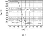
图9用以绘示电荷电流的特性曲线图。FIG. 9 is a graph showing the characteristic curve of the charge current.
【主要元件符号说明】[Description of main component symbols]
120、130:电压控制电流源120, 130: voltage controlled current source
140、150:放大器140, 150: amplifier
160:前置电路160: Front circuit
100、200:控制电路100, 200: control circuit
210、220:晶体管210, 220: Transistor
230、240:二极管230, 240: Diodes
250:电流源250: Current source
400:电流供应器400: current supply
410、420、430、440、450、540、560、570、580、730、740、830、840、841、880:晶体管410, 420, 430, 440, 450, 540, 560, 570, 580, 730, 740, 830, 840, 841, 880: Transistor
460、470、710、720、810、820:放大器460, 470, 710, 720, 810, 820: amplifier
110、480、750、760、851、850、860:电阻110, 480, 750, 760, 851, 850, 860: resistance
510、520、530:恒电流源510, 520, 530: constant current source
550:电流镜550: Current Mirror
690:恒定功率控制器690: Constant Power Controller
REF1、REF2、REF3、REF4:参考电压REF1, REF2, REF3, REF4: Reference voltage
A、B:输入端A, B: input terminal
Out:输出端Out: output terminal
ICHG、IS、I880:电流ICHG , IS , I880: Current
V1、V2、V3、V4、VBAT、PROG、VPTAT:电压V1, V2, V3, V4, VBAT, PROG, VPTAT : voltage
Z1、BAT:负载Z1, BAT: load
VC:电源供应器VC: power supply
N1:节点N1: node
Tp:预设温度Tp: preset temperature
具体实施方式Detailed ways
以下的叙述将伴随着实施例的图示,来详细对本发明所提出的实施例进行说明。在各图示中所使用相同或相似的参考标号,是用来叙述相同或相似的部分。The following description will describe the embodiments of the present invention in detail along with the illustrations of the embodiments. The same or similar reference numerals used in the drawings are used to describe the same or similar parts.
第一实施例first embodiment
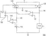
图4为依据本发明第一实施例充电器的恒电流及恒电压的电流供应器的电路图。依据本发明第一实施例恒电流及恒电压的电流供应器400提供充电电流ICHG至负载。此负载例如为可充电电池BAT。依据第一实施例恒电流及恒电压的电流供应器400包括驱动晶体管410、检测晶体管420、下拉晶体管450、恒电压控制器、恒电流控制器及外接电阻480。此恒电压控制器至少包括运算放大器460及PMOS晶体管430。此恒电流控制器至少包括运算放大器470及PMOS晶体管440。运算放大器460可以为一电压放大器(Voltage Amplifier,VA)。运算放大器470可以为一电流放大器 (Current Amplifier,CA)。FIG. 4 is a circuit diagram of the constant current and constant voltage current suppliers of the charger according to the first embodiment of the present invention. According to the first embodiment of the present invention, the constant current and constant voltage
驱动晶体管410的源极端耦接电源供应器VC,其栅极端耦节点N1,以及其漏极端耦接负载BAT。驱动晶体管410被用于提供充电电流ICHG至负载BAT。驱动晶体管410在此以PMOS晶体管为例用以说明。The source terminal of the driving
检测晶体管420的源极端耦接电源供应器VC,其栅极端耦节点N1,以及其漏极端耦接电流放大器470及电阻480。The source terminal of the
下拉晶体管450的源极端耦接接地电压,其栅极端耦接电流放大器470的输出端,以及其漏极端耦接节点N1。下拉晶体管450用以拉低节点N1的电压至接地电压。下拉晶体管410在此以NMOS晶体管为例用以说明。The source terminal of the pull-
恒电压控制器耦接驱动晶体管410、检测晶体管420及下拉晶体管450。恒电流控制器耦接驱动晶体管410、下拉晶体管450及恒电流控制器。The constant voltage controller is coupled to the driving
PMOS晶体管430为上拉晶体管。PMOS晶体管430的源极端耦接电源供应器VC,其栅极端耦接电压放大器460的输出端,以及其漏极端耦接节点N1。上拉晶体管450用以拉高节点N1的电压。
电压放大器460的第一输入端耦接参考电压REF1,其第二输入端耦接负载BAT,以及其输出端耦接上拉晶体管430的栅极端。换句话说,电压放大器460比较参考电压REF1与负载BAT的输出电压VBAT,以控制晶体管430的驱动能力。A first input terminal of the
PMOS晶体管440亦为上拉晶体管。PMOS晶体管440的源极端耦接电源供应器VC,其栅极端耦接电流放大器470的另一个输出端,以及其漏极端耦接节点N1。上拉晶体管440也被用来拉高节点N1的电压。
电压放大器470的第一输入端耦接另一参考电压REF2,其第二输入端耦接电阻480,其第一输出端耦接PMOS晶体管440的栅极端,以及其第二输出端耦接下拉晶体管450的栅极端。电压PROG为电阻480的电压。换句话说,电流放大器470比较参考电压REF2与电压PROG,以控制控制晶体管440及450的驱动能力。The first input terminal of the
一般而言,节点N1的电压会被晶体管430及440拉高。当负载BAT的电压升高并且接近参考电压REF1时(亦即充电器运作于恒电压模式),晶体管430会由于放大器460而稍微地导通,并且相应地节点N1的电压会稍微提升。同时,驱动晶体管410为微弱导通以对负载BAT充电,直到负载BAT的电压VBAT与参考电压REF1大致相等。换句话说,恒电压控制器 拉高节点N1的电压,以控制驱动晶体管410的传导状态。相应地,在电压控制模式下,负载BAT的电压VBAT会大致维持与参考电压REF1相等。Generally, the voltage of the node N1 is pulled high by the
反之,当负载BAT的电压VBAT大幅降低至低于参考电压REF1时(亦即充电器运作于恒电流模式),晶体管430会由于放大器460而关闭,同时节点N1的电压会由于晶体管450被拉低至接地电压。那么,晶体管410及420会导通,以及电压PROG会由于电流IS而提升。如果电压PROG变成高于参考电压REF2,晶体管440及450的驱动能力会各别地及同步地被增加及减少,以提升节点N1的电压。经由放大器470的回路调整执行后,电压PROG为几乎与参考电压REF2相等,亦即IS≈REF2/R480(R480参照电阻480的电阻值)。在本实施例中,晶体管410与420的尺寸比(通道长与宽的比例W/L)为1000:1。因此,充电电流ICHG≈1000×IS≈1000×(REF2/R480)。也就是说,在恒电流模式,充电电流ICHG会被限制。Conversely, when the voltage VBAT of the load BAT drops significantly below the reference voltage REF1 (that is, the charger operates in the constant current mode), the
图5为图4中的电流放大器470的电路图。请参照图5,电流放大器470包括恒电流源510、520、530、电流镜550、晶体管540、560、570及580。FIG. 5 is a circuit diagram of the
晶体管570例如为PMOS晶体管,其源极端耦接恒电流源510,其栅极端作为电流放大器470的第二输入端,以及其漏极端耦接恒电流源520。The
晶体管580例如为PMOS晶体管,其源极端耦接恒电流源510,其栅极端作为电流放大器470的第一输入端,以及其漏极端耦接恒电流源530。The
晶体管540例如为PMOS晶体管,其源极端耦接电源供应器VC,其栅极端作为电流放大器470的第一输出端,以及其漏极端耦接恒电流源530。晶体管540与晶体管440形成电流镜。The
晶体管560例如为NMOS晶体管,其源极端耦接接地电压,其栅极端作为电流放大器470的第二输出端,以及其漏极端耦接其栅极端。The
电流镜550为耦接电源供应器VC、恒电流源530及晶体管560的漏极端。第一电流镜550包括晶体管551及552。晶体管551例如为PMOS晶体管,其源极端耦接电源供应器VC,其栅极端耦接恒电流源530,以及其漏极端耦接恒电流源530。晶体管552例如为PMOS晶体管,其源极端耦接电源供应器VC,其栅极端耦接恒电流源530,以及其漏极端耦接晶体管560的漏极。The
第二实施例second embodiment
图6为依据本发明第二实施例充电器的恒电流恒电压及恒温的电流供应器的电路图。在第一与第二实施例中,相似的元件会具有相似的参考符号,以及省略其细节以简化说明。6 is a circuit diagram of a constant current, constant voltage and constant temperature current supplier of a charger according to a second embodiment of the present invention. In the first and second embodiments, similar elements are provided with similar reference numerals, and details thereof are omitted for simplicity of description.
在第二实施例中,恒定功率控制器690被用来产生及控制参考电压REF2,以达到热控制的功能。在恒电流相位中,驱动晶体管610会消耗几瓦特的功率,以及造成核心温度的浪涌效应。为了防止热扩散,当核心温度到达预设温度Tp时,驱动晶体管610的功率消耗必须限制。假如核心温度增加至大于预设温度Tp,则恒定功率控制器690会拉低参考电压REF2,以减少驱动晶体管610提供的充电电流ICHG。这样可以经由驱动晶体管610减少其功率消耗,以及相应地核心温度会低于预设温度Tp。In the second embodiment, the
图7及图8为本发明两不同实施例中恒定功率控制器690的电路图。请参照图7,恒定功率控制器690包括运算放大器710、720、晶体管730、740及分压器。此分压器包括电阻750及760。7 and 8 are circuit diagrams of the
运算放大器710的第一输入端耦接参考电压REF3,其第二输入端耦接晶体管730及分压器,以及其输出端耦接晶体管730。运算放大器710的输出控制晶体管730的驱动能力。The first input terminal of the operational amplifier 710 is coupled to the reference voltage REF3 , the second input terminal is coupled to the transistor 730 and the voltage divider, and the output terminal is coupled to the transistor 730 . The output of the operational amplifier 710 controls the drive capability of the transistor 730 .
晶体管730例如为PMOS晶体管,其源极端耦接电源供应器VC,其栅极端作为运算放大器710的输出端,以及其漏极端耦接运算放大器710的第二输入端。The transistor 730 is, for example, a PMOS transistor. Its source terminal is coupled to the power supply VC, its gate terminal serves as the output terminal of the operational amplifier 710 , and its drain terminal is coupled to the second input terminal of the operational amplifier 710 .
运算放大器720的第一输入端耦接参考电压REF4,其第二输入端耦接正温度系数电压VPTAT,以及其输出端耦接晶体管740。运算放大器720的输出控制晶体管740的驱动能力。举例来说,当核心温度低于预设温度TP时,参考电压REF4会高于正温度系数电压VPTAT,以致于晶体管740会关闭。反之,当核心温度高于预设温度TP时,正温度系数电压VPTAT会升高到高于参考电压REF4,以致于晶体管740会导通。如果核心温度越高于预设温度TP,晶体管具有的驱动能力就越强。A first input terminal of the operational amplifier 720 is coupled to the reference voltage REF4 , a second input terminal thereof is coupled to the positive temperature coefficient voltage VPTAT , and an output terminal thereof is coupled to the transistor 740 . The output of the operational amplifier 720 controls the drive capability of the transistor 740 . For example, when the core temperature is lower than the preset temperature TP , the reference voltage REF4 is higher than the positive temperature coefficient voltage VPTAT , so that the transistor 740 is turned off. On the contrary, when the core temperature is higher than the preset temperature TP , the positive temperature coefficient voltage VPTAT will increase to be higher than the reference voltage REF4 , so that the transistor 740 will be turned on. If the core temperature is higher than the preset temperature TP , the driving capability of the transistor is stronger.
晶体管730例如为NMOS晶体管,其源极端耦接接地电压,其栅极端作为运算放大器720的输出端,以及其漏极端耦接参考电压REF2。The transistor 730 is, for example, an NMOS transistor. Its source terminal is coupled to the ground voltage, its gate terminal serves as the output terminal of the operational amplifier 720 , and its drain terminal is coupled to the reference voltage REF2 .
分压器具有串联的电阻750及760。The voltage divider has resistors 750 and 760 connected in series.
当核心温度小于温度TP时,晶体管730会导通且晶体管740会关闭。分压器会产生分压至运算放大器的第二输入端以提供参考电压REF2。换句 话说,在本申请例中,REF2=REF3×R760/(R760+R750),其中R750及R760分别参照电阻750及760的电阻值。When the core temperature is lower than the temperatureTP , the transistor 730 is turned on and the transistor 740 is turned off. The voltage divider generates a divided voltage to the second input terminal of the operational amplifier to provide the reference voltage REF2. In other words, in this application example, REF2=REF3×R760/(R760+R750), wherein R750 and R760 refer to the resistance values of resistors 750 and 760, respectively.
在另一方面,当核心温度升高至大于温度TP时,参考电压REF2会被晶体管740拉低(亦即参考电压REF2会等于晶体管740的电压VDS)。晶体管730会导通且晶体管740会关闭。分压器会产生分压至运算放大器的第二输入端以提供参考电压REF2。换句话说,在本申请例中,REF2=REF3×R760/(R760+R750),其中R750及R760分别参照电阻750及760的电阻值。众所周知,在回路由于电流放大器670而变得稳定之后(请参照图6),PROG=REF2以及IS=PROG/R680(R680参照电阻680的电阻值)。所以如果参考电压REF2降低时,接着电流IS也会降低,而电荷电流ICHG也会相应地降低。换句话说,当核心温度升高至大于预设温度Tp时,电荷电流ICHG会很低,并且相应地驱动晶体管610的功率消耗也会减少,所以核心温度就能保持固定于预设温度Tp。On the other hand, when the core temperature rises above the temperature TP , the reference voltage REF2 will be pulled down by the transistor 740 (that is, the reference voltage REF2 will be equal to the voltage VDS of the transistor 740 ). Transistor 730 will be on and transistor 740 will be off. The voltage divider generates a divided voltage to the second input terminal of the operational amplifier to provide the reference voltage REF2. In other words, in this application example, REF2=REF3×R760/(R760+R750), wherein R750 and R760 refer to the resistance values of the resistors 750 and 760 respectively. As is well known, after the loop is stabilized by the current amplifier 670 (please refer to FIG. 6 ), PROG=REF2 and IS =PROG/R680 (R680 refers to the resistance value of the resistor 680). Therefore, if the reference voltage REF2 decreases, then the current IS will also decrease, and the charge current ICHG will decrease accordingly. In other words, when the core temperature rises above the preset temperature Tp, the charge current ICHG will be very low, and correspondingly the power consumption of the driving
请参照图8,恒定功率控制器690包括运算放大器810、820、晶体管830、840、841、880及分压器。在图7与图8中,相似的元件具有相似的参考符号,以及其细节描叙在此略过。Referring to FIG. 8, the
晶体管840例如为NMOS晶体管,其源极端耦接接地电压,其栅极端作为运算放大器820的输出端,以及其漏极端耦接晶体管870及880的栅极。The transistor 840 is, for example, an NMOS transistor. Its source terminal is coupled to the ground voltage, its gate terminal serves as the output terminal of the operational amplifier 820 , and its drain terminal is coupled to the gates of the transistors 870 and 880 .
晶体管870及880形成电流镜,其耦接在电源供应器VC、运算放大器810的第二输入端与晶体管841的源极端之间。The transistors 870 and 880 form a current mirror coupled between the power supply VC, the second input terminal of the operational amplifier 810 and the source terminal of the transistor 841 .
此分压器包括电阻851、850及860。电阻851耦接在晶体管830的源极端及运算放大器810的第二输入端之间。The voltage divider includes resistors 851 , 850 and 860 . The resistor 851 is coupled between the source terminal of the transistor 830 and the second input terminal of the operational amplifier 810 .
当核心温度低于预设温度Tp时,晶体管830会导通,同时晶体管840、840、870及880会关闭。分压器用以提供分压至运算放大器810的第二输入端作为参考电压REF2。换句话说,在本申请例中,REF2=REF3×R860/(R860+R850+R851),其中R860、R850及R851分别参照电阻860、850、851的电阻值。When the core temperature is lower than the preset temperature Tp, the transistor 830 is turned on, and the transistors 840, 840, 870 and 880 are turned off. The voltage divider is used to provide a divided voltage to the second input terminal of the operational amplifier 810 as the reference voltage REF2. In other words, in this application example, REF2=REF3×R860/(R860+R850+R851), wherein R860, R850 and R851 refer to the resistance values of resistors 860, 850 and 851, respectively.
如果核心温度升高至大于预设温度Tp,晶体管840及841皆会导通。晶体管840的导通用以拉低参考电压REF2,并且相应地减少提供至驱动晶体管610的电荷电流ICHG。晶体管841的导通会产生电流通过晶体管870。 此电流会被晶体管880镜射进拉高电流I880,其中电流I880为通过晶体管880通道的电流。电流I880通过电阻851会产生电压降,以拉高节点N2的电压到超过参考电压REF3。在反应输入偏移电压的改变下,放大器810会增加其输出电压,并且减少晶体管830的驱动能力,直到节点N2的电压等于参考电压REF3。此处理会连续提升温度到晶体管830完全关闭。If the core temperature rises above the preset temperature Tp, both transistors 840 and 841 are turned on. The turn-on of the transistor 840 is used to pull down the reference voltage REF2 and correspondingly reduce the charge current ICHG provided to the driving
进一步来看,在高温的案例中,通过晶体管840的电流I880会小于通过晶体管740的电流(此电流为REF3/R750)。换句话说,在高温的案例中,图8中的参考电压REF2会低于图7中的参考电压REF2。Further, in the case of high temperature, the current I880 passing through the transistor 840 will be smaller than the current passing through the transistor 740 (this current is REF3/R750). In other words, in the case of high temperature, the reference voltage REF2 in FIG. 8 will be lower than the reference voltage REF2 in FIG. 7 .
请参照图4及图6,电阻480及680为外接元件。电极P1会由于电阻480及680与节点PROG的寄生电容而产生。由于电阻480及680用来规划电荷电流,其电阻值可以具有数百次的变化。所以,电极P1的频率也会具有数百次的变化。藉此,电极P1不适于作为恒电流调整回路的区域电极,以及必须增加额外的电极P2以传送区域电极。由于电极P1不是区域电极,其必须位于高于增益频率之上以确保其稳定。一种实现的方法是拉低区域电极P2至非常低的频率。然而,此方法需要大容量的电容以产生电极P2。一种方法是使用低增益放大器的小尺寸芯片作为放大器470及670。然而,低增益放大器为容易受到偏移电压的影响。藉此,在本实施例中,电流放大器470及670会设计为输出以同步控制上拉晶体管440及640与下拉晶体管450及650。因此会于低增益放大器形成AB级区段及最小的偏移。在另一方面,电压放大器440及460的输出控制上拉晶体管460及660,此形成A级区段。然而,电压放大器460及660可使用高增益放大器以减少其A区段输出的偏移。随着电流放大器470及460具有AB级输出区段与电压放大器460及660具有高增益电压,本发明的实施例可以达到电流/电压准确、小电路尺寸及共用电极的交流补偿具有最佳的效能。本实施例还具有其他优点,例如减少恒电流模式及恒电压模式的偏移及可轻易达到交流补偿。Please refer to FIG. 4 and FIG. 6 , the
图9用以绘示电荷电流ICHG的特性曲线图。此电流通过晶体管740及780为绝对温度比例(proportional to absolute temperature,PTAT),当电荷的核心温度为大于预设温度值(例如为118℃)时,在此参考电压REF2会为线性减少至接近接地电压。由于ICHG=1000×REF2/R480,电荷电流ICHG会线性减少至0。FIG. 9 is a graph illustrating a characteristic curve of the charge current ICHG . The current passing through the transistors 740 and 780 is proportional to absolute temperature (PTAT). When the core temperature of the charge is greater than a preset temperature value (for example, 118° C.), the reference voltage REF2 will decrease linearly to close to ground voltage. Since ICHG=1000×REF2/R480, the charge current ICHG will decrease linearly to 0.
请参照图5、图7及图8,当热控制运作时,参考电压REF2会经由晶体管740及840下拉接近接地电压。如图5所示的放大器,当参考电压REF2接近0时,此放大器会具有输入动态变化下降至接地以及运作良好。Please refer to FIG. 5 , FIG. 7 and FIG. 8 , when the thermal control is in operation, the reference voltage REF2 is pulled down close to the ground voltage through the transistors 740 and 840 . The amplifier shown in Figure 5, when the reference voltage REF2 is close to 0, this amplifier has input dynamics down to ground and works well.
请参照图6,恒定功率控制器690为非直接耦接至节点N1。此简化的交流补偿由于节点N1控制于晶体管630、640及650,与恒定功率控制器的运作与否没有关联。Referring to FIG. 6, the
当参考电压REF2减少至一数值(此数值为NMOS晶体管740及780进入线性区),参考电压REF2(亦即电荷电流ICHG)的减少速率会减缓,以及参考电压REF2(亦即电荷电流ICHG)不会为0。然而,此情况只发生于非常高的环境温度下,在此情况下典型充电电池将无法再使用。藉此,在典型应用中不会介意电荷电流不为0的环境。When the reference voltage REF2 decreases to a certain value (this value is that the NMOS transistors 740 and 780 enter the linear region), the decreasing rate of the reference voltage REF2 (that is, the charge current ICHG ) will slow down, and the reference voltage REF2 (that is, the charge current ICHG ) will slow down. ) will not be 0. However, this only happens at very high ambient temperatures, where typical rechargeable batteries are no longer usable. With this, an environment where the charge current is not zero is not a concern in typical applications.
虽然本发明已以实施例公开如上,然其并非用以限定本发明,本领域技术人员,在不脱离本发明的精神和范围内,当可作些许的更动与润饰,因此本发明的保护范围当视所附权利要求书所界定者为准。Although the present invention has been disclosed as above with the embodiments, it is not intended to limit the present invention. Those skilled in the art can make some changes and modifications without departing from the spirit and scope of the present invention. Therefore, the protection of the present invention The scope is to be determined as defined by the appended claims.
Claims (15)
Translated fromChineseApplications Claiming Priority (4)
| Application Number | Priority Date | Filing Date | Title |
|---|---|---|---|
| US96964907P | 2007-09-03 | 2007-09-03 | |
| US60/969,649 | 2007-09-03 | ||
| US12/121,795US7893654B2 (en) | 2007-09-03 | 2008-05-16 | Constant-current, constant-voltage and constant-temperature current supply of a battery charger |
| US12/121,795 | 2008-05-16 |
Publications (2)
| Publication Number | Publication Date |
|---|---|
| CN101383522A CN101383522A (en) | 2009-03-11 |
| CN101383522Btrue CN101383522B (en) | 2010-12-15 |
Family
ID=40406419
Family Applications (1)
| Application Number | Title | Priority Date | Filing Date |
|---|---|---|---|
| CN2008101310160AActiveCN101383522B (en) | 2007-09-03 | 2008-08-19 | Constant current, constant voltage and constant temperature current supplier of battery charger |
Country Status (3)
| Country | Link |
|---|---|
| US (1) | US7893654B2 (en) |
| CN (1) | CN101383522B (en) |
| TW (1) | TWI358182B (en) |
Families Citing this family (22)
| Publication number | Priority date | Publication date | Assignee | Title |
|---|---|---|---|---|
| US8060904B1 (en) | 2008-02-25 | 2011-11-15 | Qurio Holdings, Inc. | Dynamic load based ad insertion |
| CN102257451B (en)* | 2008-12-16 | 2014-07-09 | 意法爱立信有限公司 | Circuit system and method of controlling power management |
| KR101543668B1 (en)* | 2009-01-07 | 2015-08-12 | 삼성전자주식회사 | Load charging circuit with smooth charge changing method |
| US8575998B2 (en)* | 2009-07-02 | 2013-11-05 | Taiwan Semiconductor Manufacturing Company, Ltd. | Voltage reference circuit with temperature compensation |
| TWI409610B (en)* | 2009-12-18 | 2013-09-21 | Green Solution Tech Co Ltd | Temperature coefficient modulating circuit and temperature compensation circuit |
| US8765306B2 (en) | 2010-03-26 | 2014-07-01 | Envia Systems, Inc. | High voltage battery formation protocols and control of charging and discharging for desirable long term cycling performance |
| US20110163716A1 (en)* | 2010-11-03 | 2011-07-07 | Ford Global Technologies, Llc | Battery Charger Temperature Control System And Method |
| CN102148520B (en)* | 2011-04-07 | 2014-04-02 | 昆山明普信息科技有限公司 | Intelligent charging circuit automatically adjusting charging current according to temperature of chip |
| CN103425167B (en)* | 2011-06-30 | 2015-07-22 | 华润矽威科技(上海)有限公司 | Constant voltage and constant current control circuit |
| JP5382069B2 (en)* | 2011-07-04 | 2014-01-08 | 株式会社安川電機 | Inverter device and electric motor drive system |
| TWI470391B (en)* | 2012-06-04 | 2015-01-21 | Issc Technologies Corp | Current regulation circuit and electronic device thereof |
| JP6453553B2 (en)* | 2014-03-26 | 2019-01-16 | 株式会社メガチップス | Current mirror circuit and receiver using the same |
| TWI511345B (en) | 2014-04-07 | 2015-12-01 | Univ Nat Taiwan Science Tech | Energy storage apparatus |
| US11303126B1 (en) | 2015-05-22 | 2022-04-12 | Michael Lee Staver | Thermal management of power delivery |
| US9674015B2 (en)* | 2015-07-13 | 2017-06-06 | Xilinx, Inc. | Circuits for and methods of generating a modulated signal in a transmitter |
| US10199842B2 (en)* | 2016-03-30 | 2019-02-05 | Intel Corporation | Power supply control system |
| TWI675279B (en) | 2018-06-04 | 2019-10-21 | 群光電能科技股份有限公司 | Constant power protection circuit and constant power protection method |
| TWI674728B (en)* | 2018-08-10 | 2019-10-11 | 茂達電子股份有限公司 | Battery charging circuit |
| US10256776B1 (en)* | 2018-08-29 | 2019-04-09 | Western Electric Export Corporation | Steered current source for single-ended class-A amplifier |
| CN111596115B (en) | 2019-02-01 | 2022-09-13 | 群光电能科技股份有限公司 | Method for measuring output current by resistance compensation and conversion circuit thereof |
| CN111864859B (en)* | 2020-08-12 | 2024-05-10 | 优动能科技(深圳)有限公司 | Lithium battery pack service life prolonging system and method with constant-current constant-voltage charge and discharge |
| CN114336849A (en)* | 2021-12-30 | 2022-04-12 | 南通宏致汽车电子科技有限公司 | An automatic control circuit system of a small charger |
Citations (3)
| Publication number | Priority date | Publication date | Assignee | Title |
|---|---|---|---|---|
| JPH03257607A (en) | 1990-03-08 | 1991-11-18 | Mitsubishi Electric Corp | Constant voltage current circuit |
| JP2002116831A (en)* | 2000-10-05 | 2002-04-19 | Sharp Corp | Constant current generating circuit |
| CN1906557A (en)* | 2004-10-08 | 2007-01-31 | 株式会社理光 | Constant-current circuit and system power source using this constant-current circuit |
Family Cites Families (3)
| Publication number | Priority date | Publication date | Assignee | Title |
|---|---|---|---|---|
| US6522118B1 (en) | 2001-04-18 | 2003-02-18 | Linear Technology Corporation | Constant-current/constant-voltage current supply |
| TWI230493B (en)* | 2002-10-11 | 2005-04-01 | Hitachi Koki Kk | Charging apparatus |
| JP3972930B2 (en)* | 2004-09-30 | 2007-09-05 | 松下電工株式会社 | Charger |
- 2008
- 2008-05-16USUS12/121,795patent/US7893654B2/enactiveActive
- 2008-07-10TWTW097126179Apatent/TWI358182B/enactive
- 2008-08-19CNCN2008101310160Apatent/CN101383522B/enactiveActive
Patent Citations (3)
| Publication number | Priority date | Publication date | Assignee | Title |
|---|---|---|---|---|
| JPH03257607A (en) | 1990-03-08 | 1991-11-18 | Mitsubishi Electric Corp | Constant voltage current circuit |
| JP2002116831A (en)* | 2000-10-05 | 2002-04-19 | Sharp Corp | Constant current generating circuit |
| CN1906557A (en)* | 2004-10-08 | 2007-01-31 | 株式会社理光 | Constant-current circuit and system power source using this constant-current circuit |
Also Published As
| Publication number | Publication date |
|---|---|
| US7893654B2 (en) | 2011-02-22 |
| US20090058393A1 (en) | 2009-03-05 |
| TWI358182B (en) | 2012-02-11 |
| TW200913434A (en) | 2009-03-16 |
| CN101383522A (en) | 2009-03-11 |
Similar Documents
| Publication | Publication Date | Title |
|---|---|---|
| CN101383522B (en) | Constant current, constant voltage and constant temperature current supplier of battery charger | |
| US10601320B2 (en) | Voltage regulators for battery operated systems | |
| US8242747B2 (en) | Charging control circuit capable of constant current charging | |
| US8629649B2 (en) | Battery charging apparatus with a common control loop for a low drop-out voltage regulator and a boost regulator | |
| US6967469B2 (en) | Battery charging method, battery charging circuit, and portable electronic device having a battery | |
| TW201347355A (en) | Battery charging circuit | |
| JP4245571B2 (en) | Charging control circuit and charging device | |
| US8339108B2 (en) | Charging systems that control power dissipation in a charging path | |
| US9553461B2 (en) | Charge control circuit, charge circuit, and mobile device | |
| CN103455067B (en) | current stabilizing circuit and electronic device thereof | |
| TW201010245A (en) | Battery systems, charging /discharging circuits and methods for controlling battery charge /discharge | |
| US8289001B2 (en) | Battery charging circuit and battery charger | |
| US8283898B2 (en) | Battery charging circuit | |
| CN100405697C (en) | Charging device | |
| US7701178B2 (en) | Charge control that keeps constant input voltage supplied to battery pack | |
| US20050275375A1 (en) | Battery charger using a depletion mode transistor to serve as a current source | |
| JP7636229B2 (en) | Charging circuit | |
| CN220544732U (en) | Constant temperature charging circuit and charger | |
| JP2013219860A (en) | Charger | |
| CN101498947B (en) | Regulator circuit and its built-in charging micro-control integrated circuit | |
| CN105515073B (en) | charging structure | |
| CN118554566A (en) | Charging control circuit and chip | |
| CN118899921A (en) | Charger circuit with thermal regulation | |
| US20110127971A1 (en) | Charging circuit | |
| TW201611469A (en) | Charging structure |
Legal Events
| Date | Code | Title | Description |
|---|---|---|---|
| C06 | Publication | ||
| PB01 | Publication | ||
| C10 | Entry into substantive examination | ||
| SE01 | Entry into force of request for substantive examination | ||
| ASS | Succession or assignment of patent right | Owner name:JINGHAO SCIENCE + TECHNOLOGY CO., LTD. Free format text:FORMER OWNER: ELITE MICROPOWER INC. Effective date:20101025 | |
| C41 | Transfer of patent application or patent right or utility model | ||
| COR | Change of bibliographic data | Free format text:CORRECT: ADDRESS; FROM: HSINCHU COUNTY, TAIWAN, CHINA TO: HSINCHU CITY, TAIWAN, CHINA | |
| TA01 | Transfer of patent application right | Effective date of registration:20101025 Address after:Hsinchu City, Taiwan, China Applicant after:Jinghao Science & Technology Co., Ltd. Address before:Hsinchu County, Taiwan, China Applicant before:Elite Micropower Inc. | |
| C14 | Grant of patent or utility model | ||
| GR01 | Patent grant |