CN101378263A - Multi-carrier digital receiver based on digital intermediate frequency and multi-carrier digital receive method - Google Patents
Multi-carrier digital receiver based on digital intermediate frequency and multi-carrier digital receive methodDownload PDFInfo
- Publication number
- CN101378263A CN101378263ACNA2007100300025ACN200710030002ACN101378263ACN 101378263 ACN101378263 ACN 101378263ACN A2007100300025 ACNA2007100300025 ACN A2007100300025ACN 200710030002 ACN200710030002 ACN 200710030002ACN 101378263 ACN101378263 ACN 101378263A
- Authority
- CN
- China
- Prior art keywords
- module
- digital
- subsystem
- carrier
- signal
- Prior art date
- Legal status (The legal status is an assumption and is not a legal conclusion. Google has not performed a legal analysis and makes no representation as to the accuracy of the status listed.)
- Granted
Links
Images


Landscapes
- Circuits Of Receivers In General (AREA)
- Superheterodyne Receivers (AREA)
Abstract
Translated fromChinese
Description
Translated fromChinese技术领域technical field
本发明涉及数字接收机系统,尤其涉及基于数字中频的多载波数字接收机及多载波数字接收方法。The invention relates to a digital receiver system, in particular to a digital intermediate frequency-based multi-carrier digital receiver and a multi-carrier digital receiving method.
背景技术Background technique
传统的基于数字中频技术的数字接收机系统(如图1所示)一般包含了射频接收子系统、数字中频处理子系统、基带信号处理子系统和后台处理子系统等。射频接收子系统实现信号从RF到IF的转换处理;数字中频处理子系统实现模拟IF到数字基带I、Q的数据处理,基带数字信号处理子系统,完成同步和解调处理,后台处理实现通信接口控制、接口电平的转换以及与外界计算机的互连等。其中,射频放大和下变频子系统一般采用超外差或是零中频的设计方式,超外差式系统的谐波和杂散抑制较难实现,而零中频式系统容易出现DC(直流)偏移。目前的接收机系统,由于需要较多的模拟电路,系统指标一致性不好,调试比较复杂,而且,无法校正由于I、Q信号相位、幅度不平衡而导致的本振泄漏,也降低了接收机的接收性能。A traditional digital receiver system based on digital IF technology (as shown in Figure 1) generally includes a radio frequency receiving subsystem, a digital IF processing subsystem, a baseband signal processing subsystem, and a background processing subsystem. The radio frequency receiving subsystem realizes the conversion and processing of signals from RF to IF; the digital intermediate frequency processing subsystem realizes data processing from analog IF to digital baseband I and Q, and the baseband digital signal processing subsystem completes synchronization and demodulation processing, and background processing realizes communication Interface control, interface level conversion and interconnection with external computers, etc. Among them, the RF amplification and down-conversion subsystems generally adopt superheterodyne or zero-IF design methods. The harmonic and spurious suppression of superheterodyne systems is difficult to achieve, while zero-IF systems are prone to DC (direct current) deviation. shift. The current receiver system, due to the need for more analog circuits, the consistency of the system indicators is not good, the debugging is more complicated, and it is impossible to correct the local oscillator leakage caused by the unbalanced phase and amplitude of the I and Q signals, which also reduces the reception receiver performance of the machine.
目前,常见的接收机主要是单载波数字接收机系统,只能对单载波信号进行接收处理。随着移动通信的发展,移动通信用户数急剧增加,运营商不得不对各种制式的移动通信系统进行扩容处理,以满足用户的通信需求,导致运营成本增加。如今的通信系统扩容处理,都是采用多载波技术,这就要求相应的移动通信产品也具有多载波处理能力。因此,数字接收机应该能实现对多载波信号的处理,以符合今后的应用需求。At present, common receivers are mainly single-carrier digital receiver systems, which can only receive and process single-carrier signals. With the development of mobile communication, the number of mobile communication users has increased sharply, and operators have to expand the capacity of mobile communication systems of various standards to meet the communication needs of users, resulting in increased operating costs. Today's communication system expansion processing uses multi-carrier technology, which requires corresponding mobile communication products to also have multi-carrier processing capabilities. Therefore, digital receivers should be able to process multi-carrier signals to meet future application requirements.
发明内容Contents of the invention
本发明的目的在于克服现有技术的缺点,提供基于数字中频的多载波数字接收机及多载波数字接收方法,本发明系统不仅能满足数字接收机对多载波信号的接收处理,而且大大提高了接收机的接收动态范围,很好的抑制带外杂散、消除本振泄漏有效减少接收机的频率偏移,有效提高接收机的接收性能。The purpose of the present invention is to overcome the shortcoming of prior art, provide multi-carrier digital receiver and multi-carrier digital receiving method based on digital intermediate frequency, the system of the present invention can not only meet the receiving processing of digital receiver to multi-carrier signal, and improve greatly The receiving dynamic range of the receiver is very good to suppress out-of-band spurs, eliminate local oscillator leakage, effectively reduce the frequency offset of the receiver, and effectively improve the receiving performance of the receiver.
本发明的目的通过下述技术方案实现:一种基于数字中频的多载波数字接收机,包括射频接收子系统、A/D转换器、数字基带信号处理子系统、自动频率控制子系统,多载波数字下变频子系统,所述射频接收子系统的输出端依次通过A/D转换器、多载波数字下变频子系统与数字基带信号处理子系统的输入端连接,所述自动频率控制子系统的输入端与数字基带信号处理子系统的输出端连接,所述自动频率控制子系统的输出端与射频接收子系统的输入端连接。还包括时钟子系统、微芯片控制子系统,所述时钟子系统、微芯片控制子系统的输出端分别与射频接收子系统、A/D转换器、多载波数字下变频子系统与数字基带信号处理子系统的另一个输入端连接。The purpose of the present invention is achieved through the following technical solutions: a digital intermediate frequency based multi-carrier digital receiver, comprising a radio frequency receiving subsystem, an A/D converter, a digital baseband signal processing subsystem, an automatic frequency control subsystem, and a multi-carrier Digital down-conversion subsystem, the output end of the radio frequency receiving subsystem is connected to the input end of the digital baseband signal processing subsystem through the A/D converter, the multi-carrier digital down-conversion subsystem in turn, and the automatic frequency control subsystem The input end is connected to the output end of the digital baseband signal processing subsystem, and the output end of the automatic frequency control subsystem is connected to the input end of the radio frequency receiving subsystem. It also includes a clock subsystem and a microchip control subsystem, the output terminals of the clock subsystem and the microchip control subsystem are respectively connected with the radio frequency receiving subsystem, the A/D converter, the multi-carrier digital down-conversion subsystem and the digital baseband signal Another input connection to the processing subsystem.
所述多载波数字下变频子系统,包括A/D采样和AGC控制模块、单通道NCO产生模块、第一级正交调制处理模块、第一级抽取滤波器组、多通道NCO产生模块、第二级复数调制处理模块、第二级抽取滤波器组、可变增益调节模块、本振抑制模块、数据格式转换模块、数据接口控制模块、DDC系统总控制模块;所述A/D采样和AGC控制模块输出端依次通过第一级正交调制处理模块、第一级抽取滤波器组、第二级复数调制处理模块、第二级抽取滤波器组、可变增益调节模块、本振抑制模块、数据格式转换模块与数据接口控制模块的输入端连接;所述单通道NCO产生模块的输出端与第一级正交调制处理模块的输入端连接;所述多通道NCO产生模块的输出端与第二级复数调制处理模块的输入端连接;所述DDC系统总控制模块的输出端同时与单通道NCO产生模块、多通道NCO产生模块、可变增益调节模块、本振抑制模块、数据格式转换模块与数据接口控制模块的另一个输入端连接。The multi-carrier digital down-conversion subsystem includes an A/D sampling and AGC control module, a single-channel NCO generation module, a first-stage orthogonal modulation processing module, a first-stage decimation filter bank, a multi-channel NCO generation module, and a first-stage quadrature modulation processing module. Two-level complex modulation processing module, second-level decimation filter bank, variable gain adjustment module, local oscillator suppression module, data format conversion module, data interface control module, DDC system total control module; the A/D sampling and AGC The output terminal of the control module sequentially passes through the first-stage quadrature modulation processing module, the first-stage decimation filter bank, the second-stage complex modulation processing module, the second-stage decimation filter bank, the variable gain adjustment module, the local oscillator suppression module, The data format conversion module is connected to the input of the data interface control module; the output of the single-channel NCO generation module is connected to the input of the first-stage orthogonal modulation processing module; the output of the multi-channel NCO generation module is connected to the first The input end of the secondary complex modulation processing module is connected; the output end of the DDC system total control module is simultaneously connected with a single-channel NCO generation module, a multi-channel NCO generation module, a variable gain adjustment module, a local vibration suppression module, and a data format conversion module Connect with the other input terminal of the data interface control module.
所述A/D采样和AGC控制模块包括AGC控制模块、A/D转换模块和控制处理模块,所述AGC控制模块的输出端通过A/D转换模块与控制处理模块输入端连接,所述控制处理模块输出端分别连接第一级正交调制处理模块输入端和AGC控制模块的输入端。The A/D sampling and AGC control module includes an AGC control module, an A/D conversion module and a control processing module, the output of the AGC control module is connected to the input of the control processing module through the A/D conversion module, and the control The output end of the processing module is respectively connected to the input end of the first-stage quadrature modulation processing module and the input end of the AGC control module.
所述第二级复数调制处理模块包括多个调制累加模块,数据时序调整处理模块,所述多个调制累加模块同时与数据时序调整处理模块连接;所述调制累加模块包括NCO信号延时处理模块,抽取滤波后I、Q信号延时处理模块,乘法器,混频后I、Q信号延时处理模块,累加器和累加后I、Q信号延时处理模块;所述多通道NCO产生模块与多个调制累加模块的NCO信号延时处理模块,乘法器,混频后I、Q信号延时处理模块,累加器与累加后I、Q信号延时处理模块依次连接;所述第一级抽取滤波器组与多个调制累加模块的抽取滤波后I、Q信号延时处理模块,乘法器,混频后I、Q信号延时处理模块,累加器,累加后I、Q信号延时处理模块,数据时序调整处理模块依次连接。The second-level complex modulation processing module includes a plurality of modulation accumulation modules and a data timing adjustment processing module, and the plurality of modulation accumulation modules are connected to the data timing adjustment processing module at the same time; the modulation accumulation module includes an NCO signal delay processing module , the I, Q signal delay processing module after extraction and filtering, the multiplier, the I and Q signal delay processing module after frequency mixing, the accumulator and the accumulated I, Q signal delay processing module; the multi-channel NCO generation module and The NCO signal delay processing module of multiple modulation and accumulation modules, the multiplier, the I and Q signal delay processing modules after frequency mixing, and the accumulator are connected to the accumulated I and Q signal delay processing modules in sequence; the first stage extraction I, Q signal delay processing module, multiplier, I, Q signal delay processing module after frequency mixing, accumulator, I, Q signal delay processing module after accumulation of filter bank and multiple modulation accumulation modules , the data timing adjustment processing modules are connected in sequence.
所述第一级抽取滤波器组或第二级抽取滤波器组分别由一个、两个或三个抽取滤波器组成;所述抽取滤波器是FIR、IIR、CIC或半带抽取滤波器;所述多载波数字下变频子系统用CPLD、EPLD、FPGA、DSP可编程逻辑器件或ASIC芯片中任意一种实现。The first-stage decimation filter bank or the second-stage decimation filter bank is composed of one, two or three decimation filters respectively; the decimation filter is FIR, IIR, CIC or half-band decimation filter; The multi-carrier digital down-conversion subsystem is realized by any one of CPLD, EPLD, FPGA, DSP programmable logic device or ASIC chip.
所述射频接收子系统包括抗混迭带通滤波器、模拟ATT、放大器、混频器、本振LO以及抗混迭滤波器,所述抗混迭带通滤波器的依次通过模拟ATT、放大器、混频器与抗混迭滤波器的输入端连接,所述本振LO的输出端与混频器的输入端连接。The radio frequency receiving subsystem includes an anti-aliasing band-pass filter, an analog ATT, an amplifier, a mixer, a local oscillator LO and an anti-aliasing filter, and the anti-aliasing band-pass filter passes through the analog ATT, the amplifier in sequence The mixer is connected to the input end of the anti-aliasing filter, and the output end of the local oscillator LO is connected to the input end of the mixer.
基于数字中频的多载波数字接收机的多载波数字接收方法,包括以下步骤:A multi-carrier digital receiving method based on a digital intermediate frequency multi-carrier digital receiver, comprising the following steps:
(1)射频接收子系统对天线所接收到的射频信号进行处理,将射频信号转变为模拟中频信号输出到A/D转换器;(1) The radio frequency receiving subsystem processes the radio frequency signal received by the antenna, converts the radio frequency signal into an analog intermediate frequency signal and outputs it to the A/D converter;
(2)A/D转换器将接收的模拟中频信号进行模数转换处理,输出高速率的数字中频信号到数字下变频子系统;(2) The A/D converter performs analog-to-digital conversion processing on the received analog intermediate frequency signal, and outputs a high-speed digital intermediate frequency signal to the digital down-conversion subsystem;
(3)多载波数字下变频子系统对数字中频信号进行数字下变频处理和载波分离,输出多载波的低速基带信号到基带信号处理子系统;(3) The multi-carrier digital down-conversion subsystem performs digital down-conversion processing and carrier separation on the digital intermediate frequency signal, and outputs multi-carrier low-speed baseband signals to the baseband signal processing subsystem;
(4)基带信号处理子系统对接收的低速基带信号进行包括同步、信道解码、载波搜索处理以及信道估计的处理,完成多载波数字信号的接收。(4) The baseband signal processing subsystem performs processing including synchronization, channel decoding, carrier search processing and channel estimation on the received low-speed baseband signal, and completes the reception of multi-carrier digital signals.
所述步骤(3)多载波数字下变频子系统对数字中频信号进行数字下变频处理和载波分离,输出多载波的低速基带信号到基带信号处理子系统,包括以下步骤:The step (3) multi-carrier digital down-conversion subsystem carries out digital down-conversion processing and carrier separation to the digital intermediate frequency signal, and outputs the low-speed baseband signal of the multi-carrier to the baseband signal processing subsystem, including the following steps:
(a)AGC控制模块将接收到模拟中频信号传送到A/D转换模块,A/D转换模块进行模数转换形成数字中频信号,控制模块根据数字中频信号的特性,输出反馈决策和控制信息到AGC控制模块,实现对A/D芯片的自动AGC控制;(a) The AGC control module transmits the received analog intermediate frequency signal to the A/D conversion module, and the A/D conversion module performs analog-to-digital conversion to form a digital intermediate frequency signal. The control module outputs feedback decision-making and control information to the AGC control module to realize automatic AGC control of A/D chip;
(b)A/D采样和AGC控制模块输出的数字中频信号输入到第一级正交调制处理模块,与单通道NCO产生模块输出的cos和sin信号进行混频调制处理,输出零中频的数字信号,零中频的数字信号进入到第一级抽取滤波器组进行数据抽取和滤波处理;(b) The digital intermediate frequency signal output by the A/D sampling and AGC control module is input to the first-stage quadrature modulation processing module, and the cos and sin signals output by the single-channel NCO generation module are mixed and modulated, and the digital of zero intermediate frequency is output Signal, the digital signal of zero intermediate frequency enters the first-stage decimation filter bank for data extraction and filtering processing;
(c)经过第一级抽取滤波器组进行抽取滤波后的数据,与多通道NCO产生模块产生的多个不同频率的cos和sin信号一起输入到第二级复数调制处理模块进行混频调制处理,形成多载波I、Q信号;多载波I、Q信号通过第二级抽取滤波器组进行进一步的数据抽取和滤波处理,输出低速的多载波基带I、Q数据;(c) The data extracted and filtered by the first-stage decimation filter bank are input to the second-stage complex modulation processing module together with multiple cos and sin signals of different frequencies generated by the multi-channel NCO generation module for mixing and modulation processing , forming multi-carrier I, Q signals; multi-carrier I, Q signals carry out further data extraction and filtering processing through the second-stage extraction filter bank, and output low-speed multi-carrier baseband I, Q data;
(d)经过两级调制后的信号经过可变增益调节模块,每个载波的增益都可以独立进行相应的调整,输出符合系统增益要求的I、Q信号;(d) The signal after the two-stage modulation passes through the variable gain adjustment module, and the gain of each carrier can be independently adjusted accordingly, and the I and Q signals that meet the system gain requirements are output;
(e)可变增益调节模块输出的信号通过本振抑制处理模块进行直流本振泄漏以及载波泄漏的抑制,然后通过数据格式转换模块控制输出信号的格式,最后再通过控制数据接口模块,输出并行、串行或交织模式的I、Q数据。(e) The signal output by the variable gain adjustment module is suppressed by the local oscillator suppression processing module for DC local oscillator leakage and carrier leakage, and then the format of the output signal is controlled by the data format conversion module, and finally the parallel output is output by the control data interface module , I, Q data in serial or interleaved mode.
所述步骤(e)输出信号的格式包括二进制补码、原码、偏移码。The format of the output signal in the step (e) includes two's complement code, original code, and offset code.
本发明与现有技术相比具有如下优点和有益效果:Compared with the prior art, the present invention has the following advantages and beneficial effects:
1、本发明采用数字中频技术,利用多载波信号处理方法,构建多载波数字下变频子系统,避免了传统数字下变频子系统的限制,实现了多载波的数字接收机系统。1. The present invention adopts digital intermediate frequency technology and utilizes multi-carrier signal processing methods to construct a multi-carrier digital down-conversion subsystem, avoiding the limitations of traditional digital down-conversion subsystems, and realizing a multi-carrier digital receiver system.
2、本发明的接收机可以结合多载波数字下变频子系统和射频接收子系统实现自动频率控制功能,根据数字信号所计算频率的偏差,然后通过调整RF的频偏,实现接收机的自动频率控制,有效减少接收机的频率偏移,提高接收机的接收灵敏度。2. The receiver of the present invention can combine the multi-carrier digital down-conversion subsystem and the radio frequency receiving subsystem to realize the automatic frequency control function, calculate the frequency deviation according to the digital signal, and then realize the automatic frequency control of the receiver by adjusting the RF frequency deviation. Control, effectively reduce the frequency offset of the receiver, and improve the receiving sensitivity of the receiver.
3、本发明降低对前端A/D器件的要求,在数字下变频处理中进行AGC控制,提高了A/D的动态范围,大大提高了接收机的接收动态范围。3. The present invention reduces the requirements on front-end A/D devices, performs AGC control in digital down-conversion processing, improves the dynamic range of A/D, and greatly improves the receiving dynamic range of the receiver.
4、数字下变频子系统易于利用可编程逻辑器件来实现,可以组建多种通信制式的中频系统,形成不同功能、制式和接口的数字接收机。4. The digital down-conversion subsystem is easy to implement with programmable logic devices, and can form intermediate frequency systems of various communication standards to form digital receivers with different functions, standards and interfaces.
5、本发明有利于采用诸如FPGA、CPLD、EPLD、DSP等可编程逻辑器件实现,可以在可编程逻辑器件中实现高性能的数字滤波、本振抑制等处理,很好的抑制带外杂散以及消除本振泄漏,大大提高接收机的性能。5. The present invention is beneficial to the realization of programmable logic devices such as FPGA, CPLD, EPLD, DSP, etc., and can realize high-performance digital filtering, local oscillator suppression and other processing in programmable logic devices, and can well suppress out-of-band spurious And eliminate the local oscillator leakage, greatly improving the performance of the receiver.
附图说明Description of drawings
图1是基于数字中频技术的数字接收机系统原理框图;Figure 1 is a block diagram of a digital receiver system based on digital intermediate frequency technology;
图2是本发明多载波数字接收机系统的结构原理图;Fig. 2 is the structural principle diagram of multi-carrier digital receiver system of the present invention;
图3是本发明多载波数字接收机系统的多载波数字下变频子系统的原理框图;Fig. 3 is the functional block diagram of the multi-carrier digital down-conversion subsystem of the multi-carrier digital receiver system of the present invention;
图4是本发明多载波数字接收机系统的多载波数字下变频子系统的第二级复数调制处理模块结构框图;Fig. 4 is the structural block diagram of the second-stage complex modulation processing module of the multi-carrier digital down-conversion subsystem of the multi-carrier digital receiver system of the present invention;
图5是本发明多载波数字接收机系统的射频接收子系统的结构图;Fig. 5 is a structural diagram of the radio frequency receiving subsystem of the multi-carrier digital receiver system of the present invention;
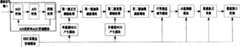
图6是多载波数字下变频系统中的N个载波NCO串行输出模式示意图;6 is a schematic diagram of NCO serial output modes of N carriers in a multi-carrier digital down-conversion system;
图7是多载波数字下变频系统中的N个载波NCO并行输出模式示意图;7 is a schematic diagram of NCO parallel output modes of N carriers in a multi-carrier digital down-conversion system;
图8是多载波数字下变频系统中的N个载波NCO突发模式NCO输出时序示意图;8 is a schematic diagram of NCO burst mode NCO output timing of N carriers in a multi-carrier digital down-conversion system;
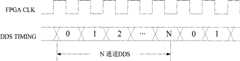
图9是多载波数字下变频系统中的N个载波并行输出模式示意图;9 is a schematic diagram of N carrier parallel output modes in a multi-carrier digital down-conversion system;
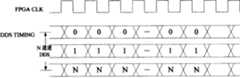
图10是多载波数字下变频系统中的N个载波并行交织输出模式示意图;Fig. 10 is a schematic diagram of N carrier parallel interleaving output modes in a multi-carrier digital down-conversion system;
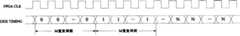
图11是多载波数字下变频系统中的N个载波串行交织输出模式示意图;Fig. 11 is a schematic diagram of N carrier serial interleaving output modes in a multi-carrier digital down-conversion system;
图12是多载波数字下变频系统中的N个载波突发模式输出时序示意图。Fig. 12 is a schematic diagram of output timing of N carriers in burst mode in a multi-carrier digital down-conversion system.
具体实施方式Detailed ways
下面结合实施例及附图对本发明作进一步详细的描述,但本发明的实施方式不限于此。The present invention will be further described in detail below in conjunction with the embodiments and the accompanying drawings, but the embodiments of the present invention are not limited thereto.
实施例Example
如图2所示,本发明一种基于数字中频的多载波数字接收机,包括射频接收子系统、A/D转换器、数字基带信号处理子系统、自动频率控制子系统,多载波数字下变频子系统,所述射频接收子系统的输出端依次通过A/D转换器、多载波数字下变频子系统与数字基带信号处理子系统的输入端连接,所述自动频率控制子系统的输入端与数字基带信号处理子系统的输出端连接,所述自动频率控制子系统的输出端与射频接收子系统的输入端连接。还包括时钟子系统、微芯片控制子系统,所述时钟子系统、微芯片控制子系统的输出端分别与射频接收子系统、A/D转换器、多载波数字下变频子系统与数字基带信号处理子系统的另一个输入端连接。As shown in Figure 2, a multi-carrier digital receiver based on digital intermediate frequency of the present invention includes a radio frequency receiving subsystem, an A/D converter, a digital baseband signal processing subsystem, an automatic frequency control subsystem, and a multi-carrier digital down-conversion Subsystem, the output end of the radio frequency receiving subsystem is connected to the input end of the digital baseband signal processing subsystem through the A/D converter, the multi-carrier digital down-conversion subsystem in turn, and the input end of the automatic frequency control subsystem is connected to the The output end of the digital baseband signal processing subsystem is connected, and the output end of the automatic frequency control subsystem is connected with the input end of the radio frequency receiving subsystem. It also includes a clock subsystem and a microchip control subsystem, the output terminals of the clock subsystem and the microchip control subsystem are respectively connected with the radio frequency receiving subsystem, the A/D converter, the multi-carrier digital down-conversion subsystem and the digital baseband signal Another input connection to the processing subsystem.
所述A/D转换器是基于数字中频技术的多载波接收机系统中关键器件之一,实现对模拟中频信号的模数转换处理,输出高速率的数字中频信号。由于数字中频处理对A/D转换器的要求较高,一般需要高速、宽动态范围的A/D器件,所以,本发明为了降低对前端A/D器件的要求,在多载波数字下变频处理中进行AGC控制,提高了A/D的动态范围。The A/D converter is one of the key devices in the multi-carrier receiver system based on digital intermediate frequency technology, which realizes analog-to-digital conversion processing of analog intermediate frequency signals and outputs high-speed digital intermediate frequency signals. Because digital intermediate frequency processing has higher requirements on A/D converters, A/D devices with high speed and wide dynamic range are generally required. Therefore, in order to reduce the requirements for front-end A/D devices, the present invention uses multi-carrier digital down-conversion processing AGC control is carried out in the middle, which improves the dynamic range of A/D.
所述基带信号处理子系统接收来自多载波信号处理的数字下变频子系统输出的基带I、Q数据,对信号进行同步、信道解码、信道估计以及载波搜索等处理。The baseband signal processing subsystem receives the baseband I and Q data output from the digital down-conversion subsystem for multi-carrier signal processing, and performs synchronization, channel decoding, channel estimation, carrier search and other processing on the signal.
所述时钟子系统为整个系统中的各个子系统和模块提供参考时钟信号,并负责数字接收机系统的时钟管理和分发,实现时钟的分频、倍频等处理;The clock subsystem provides reference clock signals for each subsystem and module in the entire system, and is responsible for clock management and distribution of the digital receiver system, and realizes clock frequency division and frequency multiplication, etc.;
所述微芯片控制子系统负责整个数字接收机系统的监测和控制,可以通过系统总线和接收机系统的各个子模块进行监控和告警处理。若某一子系统或是子模块出现工作异常,进行系统复位处理,和进行告警上报处理,微芯片控制子系统还整个系统的程序下载和更新,如FPGA、DSP程序的下载;The microchip control subsystem is responsible for the monitoring and control of the entire digital receiver system, and can perform monitoring and alarm processing through the system bus and each sub-module of the receiver system. If a certain subsystem or sub-module is working abnormally, system reset processing and alarm reporting processing are performed, and the microchip control subsystem also downloads and updates the programs of the entire system, such as downloading FPGA and DSP programs;
所述自动频率控制子系统主要实现整个接收机系统的自动频率校正,以调整接收机接收信号与输入信号的出现的频率偏差,需要根据所接收到的基带速据,计算频率的偏差,通过调节电压值来调整RF的偏差。自动频率中,所选用的晶振的控制电压需要很稳定,抗干扰。否则会导致晶振的频率不稳定。The automatic frequency control subsystem mainly implements the automatic frequency correction of the entire receiver system to adjust the frequency deviation between the received signal of the receiver and the input signal. It is necessary to calculate the frequency deviation according to the received baseband data, and adjust the Voltage value to adjust RF bias. In the automatic frequency, the control voltage of the selected crystal oscillator needs to be very stable and anti-interference. Otherwise, the frequency of the crystal oscillator will be unstable.
基于数字中频的多载波数字接收机的多载波数字接收方法,包括以下步骤:A multi-carrier digital receiving method based on a digital intermediate frequency multi-carrier digital receiver, comprising the following steps:
(1)射频接收子系统对天线所接收到的射频信号进行处理,将射频信号转变为模拟中频信号输出到A/D转换器;(1) The radio frequency receiving subsystem processes the radio frequency signal received by the antenna, converts the radio frequency signal into an analog intermediate frequency signal and outputs it to the A/D converter;
(2)A/D转换器将接收的模拟中频信号进行模数转换处理,输出高速率的数字中频信号到数字下变频子系统;(2) The A/D converter performs analog-to-digital conversion processing on the received analog intermediate frequency signal, and outputs a high-speed digital intermediate frequency signal to the digital down-conversion subsystem;
(3)多载波数字下变频子系统对数字中频信号进行数字下变频处理和载波分离,输出多载波的低速基带信号到基带信号处理子系统;(3) The multi-carrier digital down-conversion subsystem performs digital down-conversion processing and carrier separation on the digital intermediate frequency signal, and outputs multi-carrier low-speed baseband signals to the baseband signal processing subsystem;
(4)基带信号处理子系统对接收的低速基带信号进行包括同步、信道解码、载波搜索处理以及信道估计的处理,完成多载波数字信号的接收。(4) The baseband signal processing subsystem performs processing including synchronization, channel decoding, carrier search processing and channel estimation on the received low-speed baseband signal, and completes the reception of multi-carrier digital signals.
如图3所示,本发明多载波数字接收机系统的多载波数字下变频系统,包括A/D采样和AGC控制模块、单通道NCO产生模块、第一级正交调制处理模块、第一级抽取滤波器组、多通道NCO产生模块、第二级复数调制处理模块、第二级抽取滤波器组、可变增益调节模块、本振抑制模块、数据格式转换模块、数据接口控制模块、DDC系统总控制模块;所述A/D采样和AGC控制模块输出端依次通过第一级正交调制处理模块、第一级抽取滤波器组、第二级复数调制处理模块、第二级抽取滤波器组、可变增益调节模块、本振抑制模块、数据格式转换模块与数据接口控制模块的输入端连接;所述单通道NCO产生模块的输出端与第一级正交调制处理模块的输入端连接;所述多通道NCO产生模块的输出端与第二级复数调制处理模块的输入端连接;所述DDC系统总控制模块的输出端同时与单通道NCO产生模块、多通道NCO产生模块、可变增益调节模块、本振抑制模块、数据格式转换模块、数据接口控制模块的另一个输入端连接。As shown in Figure 3, the multi-carrier digital down-conversion system of the multi-carrier digital receiver system of the present invention includes an A/D sampling and AGC control module, a single-channel NCO generation module, a first-stage quadrature modulation processing module, a first-stage Decimation filter bank, multi-channel NCO generation module, second-stage complex modulation processing module, second-stage decimation filter bank, variable gain adjustment module, local oscillator suppression module, data format conversion module, data interface control module, DDC system The total control module; the A/D sampling and AGC control module output successively pass through the first-level orthogonal modulation processing module, the first-level decimation filter bank, the second-level complex modulation processing module, and the second-level decimation filter bank , the variable gain adjustment module, the local oscillator suppression module, the data format conversion module are connected to the input end of the data interface control module; the output end of the single-channel NCO generation module is connected to the input end of the first-stage quadrature modulation processing module; The output end of the multi-channel NCO generation module is connected with the input end of the second-stage complex modulation processing module; the output end of the DDC system total control module is simultaneously connected with the single-channel NCO generation module, the multi-channel NCO generation module, the variable gain The other input end of the adjustment module, the local vibration suppression module, the data format conversion module and the data interface control module is connected.
所述多载波数字下变频子系统中的A/D采样和AGC控制模块包括AGC控制模块、A/D转换模块和控制处理模块,所述AGC控制模块的输出端通过A/D转换模块与控制处理模块输入端连接,所述控制处理模块输出端分别连接第一级正交调制处理模块输入端和AGC控制模块的输入端。AGC控制模块和控制处理模块组成反馈控制系统,AGC控制模块根据控制处理模块发出的决策和控制信号,根据A/D的特性,实现对输入信号的衰减以及放大处理,以起到保护A/D转换器的同时,提高A/D转换模块的动态范围。其中控制处理模块完成输出给AGC控制的控制信号功能外,还必须具备如下一些功能:对A/D转换后的低速信号转换为适合第一级正交调制处理模块需求的高速信号,或是对A/D转换后的高速信号转换为适合第一级正交调制处理模块需求的低速信号,或是对A/D转换后的并行信号转换为适合第一级正交调制处理模块需求的串行信号,或是对A/D转换后的串行信号转换为适合第一级正交调制处理模块需求的并行信号。The A/D sampling and the AGC control module in the described multi-carrier digital down-conversion subsystem include an AGC control module, an A/D conversion module and a control processing module, and the output of the AGC control module is connected with the control module by the A/D conversion module The input end of the processing module is connected, and the output end of the control processing module is respectively connected with the input end of the first-stage quadrature modulation processing module and the input end of the AGC control module. The AGC control module and the control processing module form a feedback control system. The AGC control module realizes the attenuation and amplification processing of the input signal according to the decision-making and control signals sent by the control processing module and the characteristics of the A/D, so as to protect the A/D. At the same time as the converter, the dynamic range of the A/D conversion module is improved. In addition to the control signal function output to AGC control by the control processing module, it must also have the following functions: convert the low-speed signal after A/D conversion into a high-speed signal suitable for the requirements of the first-level quadrature modulation processing module, or The high-speed signal after A/D conversion is converted into a low-speed signal suitable for the requirements of the first-level quadrature modulation processing module, or the parallel signal after A/D conversion is converted into a serial signal suitable for the requirements of the first-level quadrature modulation processing module. signal, or convert the serial signal after A/D conversion into a parallel signal suitable for the requirements of the first-level quadrature modulation processing module.
所述第一级正交调制处理模块主要对来自A/D转换和AGC控制模块的数字中频信号以及单通道NCO产生模块所生成的单载波cos和sin信号进行第一级的混频和调制处理,输出以0MHz为中心频点的数字信号。The first-level quadrature modulation processing module mainly performs first-level mixing and modulation processing on the digital intermediate frequency signal from the A/D conversion and AGC control module and the single-carrier cos and sin signals generated by the single-channel NCO generation module , output a digital signal with 0MHz as the center frequency point.
所述单通道NCO产生模块功能是产生单载波的cos和sin信号,具体频点可以根据设计要求,由DDC系统总控制模块进行设置。The function of the single-channel NCO generation module is to generate cos and sin signals of a single carrier, and the specific frequency point can be set by the overall control module of the DDC system according to design requirements.
所述多通道NCO产生模块主要实现生成多载波的数字sin和cos信号,为第二级复数调制处理模块提供多个本振参考信号。各个载波的频点可以根据设计要求,由DDC系统总控制模块进行单独设置。多通道NCO产生模块能够输出多种时序的本振信号,如图6的N个载波NCO串行输出模式、图7的N个载波NCO并行输出模式以及图8的N个载波NCO突发模式NCO输出时序等。The multi-channel NCO generation module mainly realizes the generation of multi-carrier digital sin and cos signals, and provides multiple local oscillator reference signals for the second-stage complex modulation processing module. The frequency points of each carrier can be set individually by the overall control module of the DDC system according to the design requirements. The multi-channel NCO generation module can output local oscillator signals of various timings, such as the NCO serial output mode of N carriers shown in Figure 6, the NCO parallel output mode of N carriers shown in Figure 7, and the NCO burst mode NCO of N carriers shown in Figure 8 output timing, etc.
在多载波数字下变频系统中,为了降低A/D采样后数据的传输速率,需要采用数据抽取处理,但数据抽取会引起信号频谱的混迭,需要进行滤波。对应高倍数的抽取处理,为了降低滤波器设计的难度,节约器件资源,一般要采用多级抽取滤波器级联实现。系统中的第一级抽取滤波器组和第二级抽取滤波器组一般都是由一个或两个抽取滤波器组成,特殊情况下,会采用三个抽取滤波器来构成抽取滤波器组。其中,抽取滤波器可以为FIR、IIR以及CIC、半带抽取滤波器等。如系统第一级抽取需要实现16倍数据抽取处理,可以采用CIC抽取4倍和FIR抽取4倍来实现,也可以采用半带滤波器抽取2倍、CIC抽取2倍以及FIR抽取4倍来实现。In the multi-carrier digital down-conversion system, in order to reduce the transmission rate of the data after A/D sampling, it is necessary to use data extraction processing, but the data extraction will cause the aliasing of the signal spectrum, which needs to be filtered. Corresponding to high-multiple decimation processing, in order to reduce the difficulty of filter design and save device resources, it is generally implemented by cascading multi-stage decimation filters. The first-stage decimation filter bank and the second-stage decimation filter bank in the system are generally composed of one or two decimation filters. In special cases, three decimation filters are used to form a decimation filter bank. Wherein, the decimation filter may be FIR, IIR, CIC, half-band decimation filter, and the like. If the first stage of the system needs to achieve 16 times of data extraction processing, it can be realized by 4 times of CIC decimation and 4 times of FIR decimation, or 2 times of half-band filter decimation, 2 times of CIC decimation and 4 times of FIR decimation. .
在本发明中的多载波数字下变频子系统,对调制后的输出的信号进行增益调节和控制,以满足系统设计中对信号输入、输出增益的控制要求。所述可变增益调节模块开放了一些用户接口,以使得用户能够根据系统设计要求,任意的修改系统增益,具体可由DDC系统总控制模块实现对增益的任意调节。The multi-carrier digital down-conversion subsystem in the present invention performs gain adjustment and control on the modulated output signal to meet the control requirements for signal input and output gain in system design. The variable gain adjustment module opens some user interfaces, so that users can arbitrarily modify the system gain according to system design requirements, specifically, the gain can be adjusted arbitrarily by the DDC system general control module.
所述数据格式转换模块主要根据后续系统要求,对输出数据的格式进行一定的调整和转换,可以输出二进制补码、原码、偏移码、十六进制码等。具体输出数据格式要求,由DDC系统总控制模块进行控制和实现。The data format conversion module mainly adjusts and converts the format of the output data according to the subsequent system requirements, and can output two's complement code, original code, offset code, hexadecimal code, etc. The specific output data format requirements are controlled and realized by the total control module of the DDC system.
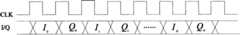
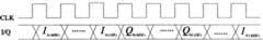
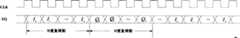
所述数据接口控制模块功能主要是输出符合后续要求的不同时序规律的基带I、Q信号。DDC系统总控制模块可以设置输出的时序要求,由数据接口控制模块实现输出如下模式的数据:如图9的N个载波并行输出模式、图10的N个载波并行交织输出模式、图11的N个载波串行交织输出模式(其中MSB(MostSignificant Bit)表征数据的最高有效位,LSB(Least Significant Bit)表征数据的最低有效位)和图12的N个载波突发模式输出时序。The main function of the data interface control module is to output baseband I and Q signals with different timing rules that meet subsequent requirements. The total control module of the DDC system can set the timing requirements of the output, and the data interface control module can output the data in the following modes: the N carrier parallel output mode shown in Figure 9, the N carrier parallel interleaved output mode shown in Figure 10, and the N carrier shown in Figure 11. A carrier serial interleaved output mode (where MSB (MostSignificant Bit) represents the most significant bit of data, LSB (Least Significant Bit) represents the least significant bit of data) and N carrier burst mode output timings in Figure 12.
所述DDC系统总控制模块分别与单通道NCO产生模块、多通道NCO产生模块、可变增益调节模块、本振抑制模块、数据格式变换模块、数据接口控制模块相连接。实现对单通道NCO产生模块和多通道NCO产生模块输出频率的设置;控制可变增益调节模块,使得各个载波的增益符合设计需求;根据系统性能要求,合理的实现本振抑制处理。最后,输出符合系统要求的数据格式和数据时序。The overall control module of the DDC system is respectively connected with a single-channel NCO generation module, a multi-channel NCO generation module, a variable gain adjustment module, a local vibration suppression module, a data format conversion module, and a data interface control module. Realize the setting of the output frequency of the single-channel NCO generation module and the multi-channel NCO generation module; control the variable gain adjustment module to make the gain of each carrier meet the design requirements; according to the system performance requirements, reasonably realize the local oscillator suppression processing. Finally, output the data format and data timing that meet the system requirements.
所述本振抑制模块在本发明中,抑制实现抵消下变频处理中,因为设计处理等所引入的直流信号以及载波泄漏信号,所以提高了多载波数字下变频系统性能。在数字下变频处理中,不可避免会引入直流信号,可以采用“对称舍入”处理方法来抑制直流泄漏,也可以采用直流滤波的方法实现对直流的抑制,还可以采用其他的方法来进行直流的抑制,如求取信号的均值,对信号进行补偿处理。而且,在多载波下变频系统中,每个频点对应的载波泄漏也会对系统性能带来较大的影响,所以,需要对载波泄漏信号进行抑制处理,以减小载波泄漏对其他载波的干扰。具体抑制要求,可以根据系统性能要求,通过DDC系统总控制模块实现任意性能的调节和控制。In the present invention, the local oscillator suppression module suppresses and implements the cancellation of the DC signal and the carrier leakage signal introduced in the down-conversion process due to the design process, so the performance of the multi-carrier digital down-conversion system is improved. In the digital down-conversion processing, it is inevitable to introduce DC signals, and the "symmetrical rounding" processing method can be used to suppress the DC leakage, or the DC filtering method can be used to suppress the DC, and other methods can be used to control the DC signal. suppression, such as finding the mean value of the signal, and compensating the signal. Moreover, in a multi-carrier down-conversion system, the carrier leakage corresponding to each frequency point will also have a greater impact on system performance. Therefore, it is necessary to suppress the carrier leakage signal to reduce the impact of carrier leakage on other carriers. interference. For specific suppression requirements, according to the system performance requirements, any performance adjustment and control can be realized through the DDC system general control module.
如图4所示,本发明多载波数字接收机系统的多载波数字下变频系统的第二级复数调制处理模块,包括多个调制累加模块,数据时序调整处理模块,所述多个调制累加模块同时与数据时序调整处理模块连接;所述调制累加模块包括NCO信号延时处理模块、抽取滤波后I、Q信号延时处理模块、乘法器、混频后I、Q信号延时处理模块、累加器和累加后I、Q信号延时处理模块;所述多通道NCO产生模块与多个调制累加模块的NCO信号延时处理模块、乘法器、混频后I、Q信号延时处理模块、累加器与累加后I、Q信号延时处理模块依次连接;所述第一级抽取滤波器组与多个调制累加模块的抽取滤波后I、Q信号延时处理模块、乘法器、混频后I、Q信号延时处理模块、累加器、累加后I、Q信号延时处理模块、数据时序调整处理模块依次连接。As shown in Figure 4, the second-stage complex modulation processing module of the multi-carrier digital down-conversion system of the multi-carrier digital receiver system of the present invention includes a plurality of modulation accumulation modules, a data timing adjustment processing module, and the plurality of modulation accumulation modules At the same time, it is connected with the data timing adjustment processing module; the modulation and accumulation module includes an NCO signal delay processing module, I and Q signal delay processing modules after extraction and filtering, a multiplier, I and Q signal delay processing modules after frequency mixing, and accumulation I, Q signal delay processing module after accumulator and accumulation; The NCO signal delay processing module, multiplier, I, Q signal delay processing module, accumulation The I and Q signal delay processing modules after the device and the accumulation are connected sequentially; the I and Q signal delay processing modules, multipliers, and I , Q signal delay processing module, accumulator, accumulated I, Q signal delay processing module, and data timing adjustment processing module are connected in sequence.
结合图3、图4所示,本发明多载波数字下变频系统实现的对数字中频信号进行数字下变频处理和载波分离,输出多载波的低速基带信号到基带信号处理子系统,包括以下步骤:3 and 4, the multi-carrier digital down-conversion system of the present invention realizes digital down-conversion processing and carrier separation for digital intermediate frequency signals, and outputs multi-carrier low-speed baseband signals to the baseband signal processing subsystem, including the following steps:
(a)AGC控制模块将接收到模拟中频信号传送到A/D转换模块,A/D转换模块进行模数转换形成数字中频信号,控制模块根据数字中频信号的特性,输出反馈决策和控制信息到AGC控制模块,实现对A/D芯片的自动AGC控制;(a) The AGC control module transmits the received analog intermediate frequency signal to the A/D conversion module, and the A/D conversion module performs analog-to-digital conversion to form a digital intermediate frequency signal. The control module outputs feedback decision-making and control information to the AGC control module to realize automatic AGC control of A/D chip;
(b)A/D采样和AGC控制模块输出的数字中频信号输入到第一级正交调制处理模块,与单通道NCO产生模块输出的cos和sin信号进行混频调制处理,输出零中频的数字信号,零中频的数字信号进入到第一级抽取滤波器组进行数据抽取和滤波处理;(b) The digital intermediate frequency signal output by the A/D sampling and AGC control module is input to the first-stage quadrature modulation processing module, and the cos and sin signals output by the single-channel NCO generation module are mixed and modulated, and the digital of zero intermediate frequency is output Signal, the digital signal of zero intermediate frequency enters the first-stage decimation filter bank for data extraction and filtering processing;
(c)经过第一级抽取滤波器组进行抽取滤波后的数据,与多通道NCO产生模块产生的多个不同频率的cos和sin信号一起输入到第二级复数调制处理模块进行混频调制处理,形成多载波I、Q信号;多载波I、Q信号通过第二级抽取滤波器组进行进一步的数据抽取和滤波处理,输出低速的多载波基带I、Q数据;(c) The data extracted and filtered by the first-stage decimation filter bank are input to the second-stage complex modulation processing module together with multiple cos and sin signals of different frequencies generated by the multi-channel NCO generation module for mixing and modulation processing , forming multi-carrier I, Q signals; multi-carrier I, Q signals carry out further data extraction and filtering processing through the second-stage extraction filter bank, and output low-speed multi-carrier baseband I, Q data;
(d)经过两级调制后的信号经过可变增益调节模块,每个载波的增益都可以独立进行相应的调整,输出符合系统增益要求的I、Q信号;(d) The signal after the two-stage modulation passes through the variable gain adjustment module, and the gain of each carrier can be independently adjusted accordingly, and the I and Q signals that meet the system gain requirements are output;
(e)可变增益调节模块输出的信号通过本振抑制处理模块进行直流本振泄漏以及载波泄漏的抑制,然后通过数据格式转换模块控制输出信号的格式,最后再通过控制数据接口模块,输出并行、串行或交织模式的I、Q数据。(e) The signal output by the variable gain adjustment module is suppressed by the local oscillator suppression processing module for DC local oscillator leakage and carrier leakage, and then the format of the output signal is controlled by the data format conversion module, and finally the parallel output is output by the control data interface module , I, Q data in serial or interleaved mode.
如图5所示,本发明基于数字中频的多载波数字接收机的射频接收子系统包括抗混迭带通滤波器、模拟ATT、放大器、混频器、本振LO以及抗混迭滤波器,所述抗混迭带通滤波器的依次通过、模拟ATT、放大器、混频器与抗混迭滤波器的输入端连接,所述本振LO的输出端与混频器的输入端连接。模拟中频信号频率范围限定在60MHz~200MHz,便于射频子系统和数字中频处理系统的设计和实现。虽然射频子系统的构成比较复杂,但这样的处理,使得输出带宽适中的宽带模拟中频信号,不需要超高速的采样,后续的A/D转换处理可以大大简化。As shown in Figure 5, the radio frequency receiving subsystem of the multi-carrier digital receiver based on the digital intermediate frequency of the present invention includes an anti-aliasing bandpass filter, an analog ATT, an amplifier, a mixer, a local oscillator LO and an anti-aliasing filter, The sequential pass, analog ATT, amplifier, and mixer of the anti-aliasing bandpass filter are connected to the input end of the anti-aliasing filter, and the output end of the local oscillator LO is connected to the input end of the mixer. The frequency range of the analog IF signal is limited to 60MHz-200MHz, which is convenient for the design and realization of the RF subsystem and the digital IF processing system. Although the composition of the radio frequency subsystem is relatively complicated, such processing enables the output of a broadband analog IF signal with a moderate bandwidth, without ultra-high-speed sampling, and the subsequent A/D conversion processing can be greatly simplified.
所述实施例为本发明较佳的实施方式,但本发明的实施方式并不受所述实施例的限制,其他的任何未背离本发明的精神实质与原理下所作的改变、修饰、替代、组合、简化,均应为等效的置换方式,都包含在本发明的保护范围之内。Said embodiment is a preferred embodiment of the present invention, but the embodiment of the present invention is not limited by said embodiment, and any other changes, modifications, substitutions, Combination and simplification should all be equivalent replacement methods, and are all included in the protection scope of the present invention.
Claims (10)
Translated fromChinesePriority Applications (1)
| Application Number | Priority Date | Filing Date | Title |
|---|---|---|---|
| CN2007100300025ACN101378263B (en) | 2007-08-31 | 2007-08-31 | Multi-carrier digital receiver based on digital intermediate frequency and multi-carrier digital receive method |
Applications Claiming Priority (1)
| Application Number | Priority Date | Filing Date | Title |
|---|---|---|---|
| CN2007100300025ACN101378263B (en) | 2007-08-31 | 2007-08-31 | Multi-carrier digital receiver based on digital intermediate frequency and multi-carrier digital receive method |
Publications (2)
| Publication Number | Publication Date |
|---|---|
| CN101378263Atrue CN101378263A (en) | 2009-03-04 |
| CN101378263B CN101378263B (en) | 2012-07-04 |
Family
ID=40421633
Family Applications (1)
| Application Number | Title | Priority Date | Filing Date |
|---|---|---|---|
| CN2007100300025AExpired - Fee RelatedCN101378263B (en) | 2007-08-31 | 2007-08-31 | Multi-carrier digital receiver based on digital intermediate frequency and multi-carrier digital receive method |
Country Status (1)
| Country | Link |
|---|---|
| CN (1) | CN101378263B (en) |
Cited By (18)
| Publication number | Priority date | Publication date | Assignee | Title |
|---|---|---|---|---|
| CN102098005A (en)* | 2010-12-13 | 2011-06-15 | 新邮通信设备有限公司 | Digital down converter and digital upconverter |
| CN102196536A (en)* | 2010-03-17 | 2011-09-21 | 鼎桥通信技术有限公司 | Method for realizing signal scanning and analysis by utilizing base station |
| CN102332927A (en)* | 2010-07-13 | 2012-01-25 | 大唐移动通信设备有限公司 | Method and device for promoting sensitivity of receiver |
| CN103051347A (en)* | 2011-09-15 | 2013-04-17 | 波音公司 | Low power radio frequency to digital receiver |
| CN103248593A (en)* | 2012-02-09 | 2013-08-14 | 泰凌微电子(上海)有限公司 | Method and system for frequency offset estimation and elimination |
| CN103582106A (en)* | 2012-07-23 | 2014-02-12 | 京信通信系统(中国)有限公司 | Signal processing method and device based on dual-carrier frequency-hopping technology and tower mounted amplifier based on dual-carrier frequency-hopping technology |
| CN103957019A (en)* | 2014-04-22 | 2014-07-30 | 熊猫电子集团有限公司 | Gain control device and method of digital receiver |
| CN104378130A (en)* | 2014-11-26 | 2015-02-25 | 成都中远信电子科技有限公司 | Receiving terminal for unmanned aerial vehicle land-to-air wideband communication system |
| CN104393885A (en)* | 2014-11-26 | 2015-03-04 | 成都中远信电子科技有限公司 | Receiving terminal and method for ground-air broadband communication system for unmanned aerial vehicle |
| CN106059981A (en)* | 2016-06-23 | 2016-10-26 | 中国科学院电子学研究所 | Demodulation method and device |
| CN106226715A (en)* | 2016-09-12 | 2016-12-14 | 厦门大学 | Resonance digital receives system |
| CN106664274A (en)* | 2014-08-21 | 2017-05-10 | 索尼公司 | Signal processing device and method |
| CN106921367A (en)* | 2017-03-03 | 2017-07-04 | 重庆湃芯微电子有限公司 | A kind of decimation filter of digital of sigma delta ADC |
| CN107346978A (en)* | 2016-05-05 | 2017-11-14 | 北京化工大学 | A kind of two-layer configuration transmitter system based on digital if technology |
| CN107425865A (en)* | 2017-04-18 | 2017-12-01 | 中国电子科技集团公司第四十研究所 | A kind of reception device of LTE A terminal signalings |
| CN109428849A (en)* | 2017-09-04 | 2019-03-05 | 瑞昱半导体股份有限公司 | Apparatus and method for processing signal interference |
| CN109547379A (en)* | 2018-12-13 | 2019-03-29 | 中国电子科技集团公司第四十研究所 | A kind of device of LTE-A MIMO signal carrier wave polymerization demodulation |
| CN114513281A (en)* | 2020-11-17 | 2022-05-17 | 大唐移动通信设备有限公司 | Multi-carrier data processing method, device and storage medium |
Family Cites Families (3)
| Publication number | Priority date | Publication date | Assignee | Title |
|---|---|---|---|---|
| EP1187387A1 (en)* | 2000-09-08 | 2002-03-13 | Alcatel | Multicarrier GSM receiver |
| CN100521672C (en)* | 2005-05-25 | 2009-07-29 | 北京北方烽火科技有限公司 | Automatic gain control device in use for multicarrier receiver |
| CN201114162Y (en)* | 2007-08-31 | 2008-09-10 | 京信通信系统(中国)有限公司 | A Multicarrier Digital Receiver System Based on Digital IF Technology |
- 2007
- 2007-08-31CNCN2007100300025Apatent/CN101378263B/ennot_activeExpired - Fee Related
Cited By (29)
| Publication number | Priority date | Publication date | Assignee | Title |
|---|---|---|---|---|
| CN102196536A (en)* | 2010-03-17 | 2011-09-21 | 鼎桥通信技术有限公司 | Method for realizing signal scanning and analysis by utilizing base station |
| CN102196536B (en)* | 2010-03-17 | 2013-07-10 | 鼎桥通信技术有限公司 | Method for realizing signal scanning and analysis by utilizing base station |
| CN102332927A (en)* | 2010-07-13 | 2012-01-25 | 大唐移动通信设备有限公司 | Method and device for promoting sensitivity of receiver |
| CN102332927B (en)* | 2010-07-13 | 2013-12-11 | 大唐移动通信设备有限公司 | Method and device for promoting sensitivity of receiver |
| CN102098005B (en)* | 2010-12-13 | 2013-08-21 | 新邮通信设备有限公司 | Digital down converter and digital upconverter |
| CN102098005A (en)* | 2010-12-13 | 2011-06-15 | 新邮通信设备有限公司 | Digital down converter and digital upconverter |
| CN103051347B (en)* | 2011-09-15 | 2016-09-07 | 波音公司 | Radio frequency digital receiver and the method being used for reducing radio frequency digital receiver power consumption |
| CN103051347A (en)* | 2011-09-15 | 2013-04-17 | 波音公司 | Low power radio frequency to digital receiver |
| CN103248593A (en)* | 2012-02-09 | 2013-08-14 | 泰凌微电子(上海)有限公司 | Method and system for frequency offset estimation and elimination |
| CN103248593B (en)* | 2012-02-09 | 2017-11-07 | 泰凌微电子(上海)有限公司 | Offset estimation and removing method and system |
| CN103582106A (en)* | 2012-07-23 | 2014-02-12 | 京信通信系统(中国)有限公司 | Signal processing method and device based on dual-carrier frequency-hopping technology and tower mounted amplifier based on dual-carrier frequency-hopping technology |
| CN103582106B (en)* | 2012-07-23 | 2017-02-08 | 京信通信系统(中国)有限公司 | Signal processing method and device based on dual-carrier frequency-hopping technology and tower mounted amplifier based on dual-carrier frequency-hopping technology |
| CN103957019B (en)* | 2014-04-22 | 2016-08-24 | 熊猫电子集团有限公司 | The gain control of digital receiver and method |
| CN103957019A (en)* | 2014-04-22 | 2014-07-30 | 熊猫电子集团有限公司 | Gain control device and method of digital receiver |
| CN106664274A (en)* | 2014-08-21 | 2017-05-10 | 索尼公司 | Signal processing device and method |
| CN106664274B (en)* | 2014-08-21 | 2020-06-30 | 索尼公司 | Signal processing apparatus and method |
| CN104378130A (en)* | 2014-11-26 | 2015-02-25 | 成都中远信电子科技有限公司 | Receiving terminal for unmanned aerial vehicle land-to-air wideband communication system |
| CN104393885B (en)* | 2014-11-26 | 2016-08-31 | 成都中远信电子科技有限公司 | A kind of reception terminal for unmanned plane ground-to-air wideband communication system and method thereof |
| CN104393885A (en)* | 2014-11-26 | 2015-03-04 | 成都中远信电子科技有限公司 | Receiving terminal and method for ground-air broadband communication system for unmanned aerial vehicle |
| CN107346978A (en)* | 2016-05-05 | 2017-11-14 | 北京化工大学 | A kind of two-layer configuration transmitter system based on digital if technology |
| CN106059981A (en)* | 2016-06-23 | 2016-10-26 | 中国科学院电子学研究所 | Demodulation method and device |
| CN106226715A (en)* | 2016-09-12 | 2016-12-14 | 厦门大学 | Resonance digital receives system |
| CN106921367A (en)* | 2017-03-03 | 2017-07-04 | 重庆湃芯微电子有限公司 | A kind of decimation filter of digital of sigma delta ADC |
| CN106921367B (en)* | 2017-03-03 | 2020-11-24 | 重庆湃芯创智微电子有限公司 | A digital decimation filter for sigma delta ADC |
| CN107425865A (en)* | 2017-04-18 | 2017-12-01 | 中国电子科技集团公司第四十研究所 | A kind of reception device of LTE A terminal signalings |
| CN109428849A (en)* | 2017-09-04 | 2019-03-05 | 瑞昱半导体股份有限公司 | Apparatus and method for processing signal interference |
| CN109547379A (en)* | 2018-12-13 | 2019-03-29 | 中国电子科技集团公司第四十研究所 | A kind of device of LTE-A MIMO signal carrier wave polymerization demodulation |
| CN114513281A (en)* | 2020-11-17 | 2022-05-17 | 大唐移动通信设备有限公司 | Multi-carrier data processing method, device and storage medium |
| CN114513281B (en)* | 2020-11-17 | 2023-06-23 | 大唐移动通信设备有限公司 | Multi-carrier data processing method, device and storage medium |
Also Published As
| Publication number | Publication date |
|---|---|
| CN101378263B (en) | 2012-07-04 |
Similar Documents
| Publication | Publication Date | Title |
|---|---|---|
| CN101378263B (en) | Multi-carrier digital receiver based on digital intermediate frequency and multi-carrier digital receive method | |
| CN101075814B (en) | Digital receiver system based on special digital medium-frequency structure | |
| CN101833100B (en) | Method for constructing fully-digital GNSS compatible navigation receiver | |
| CN101188590B (en) | Digital downlink frequency conversion system and digital downlink frequency conversion method in multi-carrier signal processing | |
| EP1336246B1 (en) | Direct conversion receiver | |
| CN100593913C (en) | Multi-carrier transmitter and multi-carrier transmission method based on digital intermediate frequency technology | |
| US20070060077A1 (en) | Receiver architecture for wireless communication | |
| CN101515807B (en) | Digital intermediate-frequency receiver | |
| CN210958360U (en) | Signal processing circuit and antenna device | |
| JP4836041B2 (en) | Method and apparatus for sampling an RF signal | |
| US7558548B2 (en) | Method and apparatus for receiving and/or down converting high frequency signals in multi mode/ multi band applications, using mixer and sampler | |
| CN111711457A (en) | A method for improving demodulation bandwidth through multi-channel parallel segment demodulation | |
| KR20060121126A (en) | Bandpass Sampling Receivers and Sampling Methods | |
| CN201114162Y (en) | A Multicarrier Digital Receiver System Based on Digital IF Technology | |
| US8605222B2 (en) | Receiver device, tuner, and television receiver | |
| CN201048372Y (en) | Special digital intermediate frequency structure based digital receiver system | |
| CN111683028B (en) | Digital equal-amplitude cw signal demodulation method | |
| US7751303B2 (en) | Demodulation circuit for use in receiver using if directing sampling scheme | |
| CN101151810B (en) | Low-IF Receiver and Its Sampling Method | |
| US7953184B2 (en) | Direct sampling type wireless receiver and method using the same | |
| CN103124247A (en) | Signal demodulating system, receiver and demodulation filtering method | |
| CN101917376B (en) | Two-stage frequency conversion method for digital down conversion system in multi-carrier digital receiver | |
| CN201114160Y (en) | Multi-carrier Transmitter Based on Digital IF Technology | |
| CN111510173A (en) | A method and device for separating received signals of a multi-channel radio station, and an analog radio host | |
| CN116743537B (en) | USB signal demodulation method based on software radio |
Legal Events
| Date | Code | Title | Description |
|---|---|---|---|
| C06 | Publication | ||
| PB01 | Publication | ||
| C10 | Entry into substantive examination | ||
| SE01 | Entry into force of request for substantive examination | ||
| C14 | Grant of patent or utility model | ||
| GR01 | Patent grant | ||
| CF01 | Termination of patent right due to non-payment of annual fee | Granted publication date:20120704 Termination date:20150831 | |
| EXPY | Termination of patent right or utility model |