CN101378229A - DC-DC converter and organic light emitting display using the same - Google Patents
DC-DC converter and organic light emitting display using the sameDownload PDFInfo
- Publication number
- CN101378229A CN101378229ACNA2008102124427ACN200810212442ACN101378229ACN 101378229 ACN101378229 ACN 101378229ACN A2008102124427 ACNA2008102124427 ACN A2008102124427ACN 200810212442 ACN200810212442 ACN 200810212442ACN 101378229 ACN101378229 ACN 101378229A
- Authority
- CN
- China
- Prior art keywords
- voltage
- output
- constructed
- supply voltage
- capacitor
- Prior art date
- Legal status (The legal status is an assumption and is not a legal conclusion. Google has not performed a legal analysis and makes no representation as to the accuracy of the status listed.)
- Pending
Links
- 239000003990capacitorSubstances0.000claimsabstractdescription80
- 238000010586diagramMethods0.000description16
- 238000007599dischargingMethods0.000description3
- 230000002411adverseEffects0.000description2
- 230000000694effectsEffects0.000description2
- 238000004904shorteningMethods0.000description2
- 230000002159abnormal effectEffects0.000description1
- 230000000903blocking effectEffects0.000description1
- 230000001934delayEffects0.000description1
- 238000000113differential scanning calorimetryMethods0.000description1
- 239000004973liquid crystal related substanceSubstances0.000description1
- 238000004020luminiscence typeMethods0.000description1
- 238000000034methodMethods0.000description1
- 238000012986modificationMethods0.000description1
- 230000004048modificationEffects0.000description1
- 229920001690polydopaminePolymers0.000description1
- 238000005215recombinationMethods0.000description1
- 230000006798recombinationEffects0.000description1
Images


Classifications
- H—ELECTRICITY
- H05—ELECTRIC TECHNIQUES NOT OTHERWISE PROVIDED FOR
- H05B—ELECTRIC HEATING; ELECTRIC LIGHT SOURCES NOT OTHERWISE PROVIDED FOR; CIRCUIT ARRANGEMENTS FOR ELECTRIC LIGHT SOURCES, IN GENERAL
- H05B45/00—Circuit arrangements for operating light-emitting diodes [LED]
- H05B45/60—Circuit arrangements for operating LEDs comprising organic material, e.g. for operating organic light-emitting diodes [OLED] or polymer light-emitting diodes [PLED]
- G—PHYSICS
- G09—EDUCATION; CRYPTOGRAPHY; DISPLAY; ADVERTISING; SEALS
- G09G—ARRANGEMENTS OR CIRCUITS FOR CONTROL OF INDICATING DEVICES USING STATIC MEANS TO PRESENT VARIABLE INFORMATION
- G09G3/00—Control arrangements or circuits, of interest only in connection with visual indicators other than cathode-ray tubes
- G09G3/20—Control arrangements or circuits, of interest only in connection with visual indicators other than cathode-ray tubes for presentation of an assembly of a number of characters, e.g. a page, by composing the assembly by combination of individual elements arranged in a matrix no fixed position being assigned to or needed to be assigned to the individual characters or partial characters
- G09G3/22—Control arrangements or circuits, of interest only in connection with visual indicators other than cathode-ray tubes for presentation of an assembly of a number of characters, e.g. a page, by composing the assembly by combination of individual elements arranged in a matrix no fixed position being assigned to or needed to be assigned to the individual characters or partial characters using controlled light sources
- G09G3/30—Control arrangements or circuits, of interest only in connection with visual indicators other than cathode-ray tubes for presentation of an assembly of a number of characters, e.g. a page, by composing the assembly by combination of individual elements arranged in a matrix no fixed position being assigned to or needed to be assigned to the individual characters or partial characters using controlled light sources using electroluminescent panels
- G09G3/32—Control arrangements or circuits, of interest only in connection with visual indicators other than cathode-ray tubes for presentation of an assembly of a number of characters, e.g. a page, by composing the assembly by combination of individual elements arranged in a matrix no fixed position being assigned to or needed to be assigned to the individual characters or partial characters using controlled light sources using electroluminescent panels semiconductive, e.g. using light-emitting diodes [LED]
- G09G3/3208—Control arrangements or circuits, of interest only in connection with visual indicators other than cathode-ray tubes for presentation of an assembly of a number of characters, e.g. a page, by composing the assembly by combination of individual elements arranged in a matrix no fixed position being assigned to or needed to be assigned to the individual characters or partial characters using controlled light sources using electroluminescent panels semiconductive, e.g. using light-emitting diodes [LED] organic, e.g. using organic light-emitting diodes [OLED]
- H—ELECTRICITY
- H02—GENERATION; CONVERSION OR DISTRIBUTION OF ELECTRIC POWER
- H02M—APPARATUS FOR CONVERSION BETWEEN AC AND AC, BETWEEN AC AND DC, OR BETWEEN DC AND DC, AND FOR USE WITH MAINS OR SIMILAR POWER SUPPLY SYSTEMS; CONVERSION OF DC OR AC INPUT POWER INTO SURGE OUTPUT POWER; CONTROL OR REGULATION THEREOF
- H02M3/00—Conversion of DC power input into DC power output
- H02M3/003—Constructional details, e.g. physical layout, assembly, wiring or busbar connections
- G—PHYSICS
- G09—EDUCATION; CRYPTOGRAPHY; DISPLAY; ADVERTISING; SEALS
- G09G—ARRANGEMENTS OR CIRCUITS FOR CONTROL OF INDICATING DEVICES USING STATIC MEANS TO PRESENT VARIABLE INFORMATION
- G09G2330/00—Aspects of power supply; Aspects of display protection and defect management
- G09G2330/02—Details of power systems and of start or stop of display operation
- G09G2330/021—Power management, e.g. power saving
- G—PHYSICS
- G09—EDUCATION; CRYPTOGRAPHY; DISPLAY; ADVERTISING; SEALS
- G09G—ARRANGEMENTS OR CIRCUITS FOR CONTROL OF INDICATING DEVICES USING STATIC MEANS TO PRESENT VARIABLE INFORMATION
- G09G2330/00—Aspects of power supply; Aspects of display protection and defect management
- G09G2330/02—Details of power systems and of start or stop of display operation
- G09G2330/027—Arrangements or methods related to powering off a display
- G—PHYSICS
- G09—EDUCATION; CRYPTOGRAPHY; DISPLAY; ADVERTISING; SEALS
- G09G—ARRANGEMENTS OR CIRCUITS FOR CONTROL OF INDICATING DEVICES USING STATIC MEANS TO PRESENT VARIABLE INFORMATION
- G09G2330/00—Aspects of power supply; Aspects of display protection and defect management
- G09G2330/02—Details of power systems and of start or stop of display operation
- G09G2330/028—Generation of voltages supplied to electrode drivers in a matrix display other than LCD
- G—PHYSICS
- G09—EDUCATION; CRYPTOGRAPHY; DISPLAY; ADVERTISING; SEALS
- G09G—ARRANGEMENTS OR CIRCUITS FOR CONTROL OF INDICATING DEVICES USING STATIC MEANS TO PRESENT VARIABLE INFORMATION
- G09G2330/00—Aspects of power supply; Aspects of display protection and defect management
- G09G2330/04—Display protection
- Y—GENERAL TAGGING OF NEW TECHNOLOGICAL DEVELOPMENTS; GENERAL TAGGING OF CROSS-SECTIONAL TECHNOLOGIES SPANNING OVER SEVERAL SECTIONS OF THE IPC; TECHNICAL SUBJECTS COVERED BY FORMER USPC CROSS-REFERENCE ART COLLECTIONS [XRACs] AND DIGESTS
- Y02—TECHNOLOGIES OR APPLICATIONS FOR MITIGATION OR ADAPTATION AGAINST CLIMATE CHANGE
- Y02B—CLIMATE CHANGE MITIGATION TECHNOLOGIES RELATED TO BUILDINGS, e.g. HOUSING, HOUSE APPLIANCES OR RELATED END-USER APPLICATIONS
- Y02B20/00—Energy efficient lighting technologies, e.g. halogen lamps or gas discharge lamps
- Y02B20/30—Semiconductor lamps, e.g. solid state lamps [SSL] light emitting diodes [LED] or organic LED [OLED]
Landscapes
- Engineering & Computer Science (AREA)
- Physics & Mathematics (AREA)
- Computer Hardware Design (AREA)
- General Physics & Mathematics (AREA)
- Theoretical Computer Science (AREA)
- Power Engineering (AREA)
- Electroluminescent Light Sources (AREA)
- Control Of Indicators Other Than Cathode Ray Tubes (AREA)
- Control Of El Displays (AREA)
- Dc-Dc Converters (AREA)
Abstract
Translated fromChinese
Description
Translated fromChinese技术领域technical field
本发明涉及一种DC-DC转换器(直流-直流转换器)及利用该DC-DC转换器的有机发光显示器,更具体地讲,涉及一种DC-DC转换器及利用该DC-DC转换器的有机发光显示器,以防止有机发光显示器中的异常显示。The present invention relates to a DC-DC converter (DC-DC converter) and an organic light-emitting display using the DC-DC converter, more specifically, to a DC-DC converter and a DC-DC converter using the DC-DC converter organic light-emitting display device to prevent abnormal display in the organic light-emitting display.
背景技术Background technique
阴极射线管的缺点在于重量和体积大,近来,开发了各种重量减轻且体积减小的平板显示装置。平板显示装置包括液晶显示器(LCD)、场发射显示器(FED)、等离子体显示面板(PDP)和有机发光显示器(OLED)等。Cathode ray tubes are disadvantageous in that they are large in weight and volume, and recently, various flat panel display devices having reduced weight and volume have been developed. Flat panel display devices include liquid crystal displays (LCDs), field emission displays (FEDs), plasma display panels (PDPs), organic light emitting displays (OLEDs), and the like.
在所述平板显示装置中,有机发光显示器利用有机发光二极管(OLED)来显示图像,其中,有机发光二极管(OLED)通过电子与空穴的复合来产生光。这种有机发光显示器的市场具有包括色彩还原性优良和厚度薄等的若干优点,并已拓展到除了手机应用之外的PDA、MP3、DSC等应用。Among the flat panel display devices, the organic light emitting display displays images using organic light emitting diodes (OLEDs) that generate light through recombination of electrons and holes. The market for such organic light emitting displays has several advantages including excellent color reproduction and thin thickness, and has expanded to applications such as PDAs, MP3s, DSCs, etc. in addition to mobile phone applications.
图1是示出用于有机发光显示器的像素的电路图。参照图1,该像素包括第一晶体管M1、第二晶体管M2、电容器Cst和有机发光二极管OLED。FIG. 1 is a circuit diagram illustrating a pixel for an organic light emitting display. Referring to FIG. 1, the pixel includes a first transistor M1, a second transistor M2, a capacitor Cst, and an organic light emitting diode OLED.
第一晶体管M1的源极连接到第一电源ELVDD,第一晶体管M1的漏极连接到有机发光二极管OLED,第一晶体管M1的栅极连接到节点N1。第二晶体管M2的源极连接到数据线Dm,第二晶体管M2的漏极连接到节点N1,第二晶体管M2的栅极连接到扫描线Sn。电容器Cst的第一电极连接到第一电源ELVDD,电容器Cst的第二电极连接到节点N1。有机发光二极管OLED包括阳极电极、阴极电极和发光层,其中,阳极电极连接到第一晶体管M1的漏极,阴极电极连接到第二电源ELVSS。如果电流从有机发光二极管OLED的阳极电极流到有机发光二极管OLED的阴极电极,则发光层对应于流过的电流的量而发光。等式1表示流入第一晶体管M1的漏极的电流。The source of the first transistor M1 is connected to the first power supply ELVDD, the drain of the first transistor M1 is connected to the organic light emitting diode OLED, and the gate of the first transistor M1 is connected to the node N1. The source of the second transistor M2 is connected to the data line Dm, the drain of the second transistor M2 is connected to the node N1, and the gate of the second transistor M2 is connected to the scan line Sn. A first electrode of the capacitor Cst is connected to the first power source ELVDD, and a second electrode of the capacitor Cst is connected to the node N1. The organic light emitting diode OLED includes an anode electrode, a cathode electrode connected to the drain of the first transistor M1, and a cathode electrode connected to the second power source ELVSS, and a light emitting layer. If a current flows from the anode electrode of the organic light emitting diode OLED to the cathode electrode of the organic light emitting diode OLED, the light emitting layer emits light corresponding to the amount of the flowing current.
这里,Id表示流入第一晶体管M1的漏极的电流,Vdata表示数据信号的电压,ELVDD表示第一电源在第一晶体管M1的源极处的电压,Vth表示第一晶体管M1的阈值电压,β代表常数。Here,Id represents the current flowing into the drain of the first transistor M1, Vdata represents the voltage of the data signal, ELVDD represents the voltage of the first power supply at the source of the first transistor M1, Vth represents the threshold voltage of the first transistor M1, β represents a constant.
如果有机发光显示器的像素被供应有第一电压ELVDD和第二电压ELVSS,则即使没有发送数据信号时,也有一定的电压通过电容器Cst被施加到第一晶体管M1的栅极。因此,电流流入有机发光二极管OLED,从而像素发光。然而,该发光是不必要的发光,从而缩短了像素的寿命。If the pixels of the organic light emitting display are supplied with the first voltage ELVDD and the second voltage ELVSS, a certain voltage is applied to the gate of the first transistor M1 through the capacitor Cst even when no data signal is transmitted. Accordingly, current flows into the organic light emitting diode OLED so that the pixel emits light. However, this light emission is unnecessary light emission, thereby shortening the lifetime of the pixel.
发明内容Contents of the invention
一方面在于提供一种DC-DC转换器,该DC-DC转换器包括:电压发生器,被构造为通过输入端接收输入电压,以产生第一电源电压和第二电源电压,并分别通过第一输出端和第二输出端输出第一电源电压和第二电源电压,其中,第二电源电压小于第一电源电压,电压发生器被构造为根据接收的控制信号产生第一电源电压和第二电源电压;电容器,连接到第一输出端和第二输出端中的至少一个;开关单元,被构造为根据控制信号使电容器放电。One aspect is to provide a DC-DC converter, the DC-DC converter includes: a voltage generator configured to receive an input voltage through an input terminal to generate a first power supply voltage and a second power supply voltage, and respectively pass the first power supply voltage and the second power supply voltage An output terminal and a second output terminal output a first power supply voltage and a second power supply voltage, wherein the second power supply voltage is smaller than the first power supply voltage, and the voltage generator is configured to generate the first power supply voltage and the second power supply voltage according to the received control signal a power supply voltage; a capacitor connected to at least one of the first output terminal and the second output terminal; and a switching unit configured to discharge the capacitor according to the control signal.
另一方面在于提供一种DC-DC转换器,该DC-DC转换器包括:电压发生器,被构造为通过输入端接收输入电压,以产生第一电源电压和第二电源电压,并通过第一输出端和第二输出端输出第一电源电压和第二电源电压,其中,第二电源电压小于第一电源电压,基于控制信号选择性地产生第一电源电压和第二电源电压;电容器,连接到第一输出端和第二输出端中的至少一个;电阻器,连接到第一输出端和第二输出端中的至少一个以及地,并被构造为释放存储在电容器中的电压。Another aspect is to provide a DC-DC converter, the DC-DC converter includes: a voltage generator configured to receive an input voltage through an input terminal to generate a first power supply voltage and a second power supply voltage, and generate a first power supply voltage and a second power supply voltage through a second power supply voltage. An output terminal and a second output terminal output a first power supply voltage and a second power supply voltage, wherein the second power supply voltage is smaller than the first power supply voltage, and the first power supply voltage and the second power supply voltage are selectively generated based on a control signal; the capacitor, connected to at least one of the first output terminal and the second output terminal; a resistor connected to at least one of the first output terminal and the second output terminal and ground and configured to discharge the voltage stored in the capacitor.
另一方面在于提供一种有机发光显示器,该有机发光显示器包括:像素单元,被构造为基于接收的数据信号、扫描信号以及第一电源电压和第二电源电压来显示图像;数据驱动器,被构造为产生数据信号;扫描驱动器,被构造为产生扫描信号;DC-DC转换器,被构造为产生第一电源电压和第二电源电压。其中,所述DC-DC转换器包括:电压发生器,被构造为通过输入端接收输入电压,以产生第一电源电压和第二电源电压,并通过第一输出端和第二输出端输出第一电源电压和第二电源电压,其中,第二电源电压小于第一电源电压,基于控制信号选择性地产生第一电源电压和第二电源电压;电容器,连接到第一输出端和第二输出端中的至少一个;开关单元,被构造为根据控制信号释放存储在电容器中的电压。Another aspect is to provide an organic light emitting display, which includes: a pixel unit configured to display an image based on a received data signal, a scan signal, and a first power supply voltage and a second power supply voltage; a data driver configured To generate the data signal; the scan driver is configured to generate the scan signal; the DC-DC converter is configured to generate the first power supply voltage and the second power supply voltage. Wherein, the DC-DC converter includes: a voltage generator configured to receive an input voltage through an input terminal to generate a first power supply voltage and a second power supply voltage, and output a first power supply voltage through a first output terminal and a second output terminal a power supply voltage and a second power supply voltage, wherein the second power supply voltage is smaller than the first power supply voltage, the first power supply voltage and the second power supply voltage are selectively generated based on the control signal; a capacitor connected to the first output terminal and the second output terminal At least one of the terminals; a switch unit configured to release the voltage stored in the capacitor according to a control signal.
另一方面在于提供一种有机发光显示器,该有机发光显示器包括:像素单元,被构造为基于接收的数据信号、扫描信号以及第一电源电压和第二电源电压来显示图像;数据驱动器,被构造为产生数据信号;扫描驱动器,被构造为产生扫描信号;DC-DC转换器,被构造为产生第一电源电压和第二电源电压。其中,所述DC-DC转换器包括:电压发生器,被构造为通过输入端接收输入电压,以产生第一电源电压和第二电源电压,并通过第一输出端和第二输出端输出第一电源电压和第二电源电压,其中,第二电源电压小于第一电源电压,基于控制信号选择性地产生第一电源电压和第二电源电压;电容器,连接到第一输出端和第二输出端中的至少一个;电阻器,连接到第一输出端和第二输出端中的至少一个以及地,并被构造为释放存储在电容器中的电压。Another aspect is to provide an organic light emitting display, which includes: a pixel unit configured to display an image based on a received data signal, a scan signal, and a first power supply voltage and a second power supply voltage; a data driver configured To generate the data signal; the scan driver is configured to generate the scan signal; the DC-DC converter is configured to generate the first power supply voltage and the second power supply voltage. Wherein, the DC-DC converter includes: a voltage generator configured to receive an input voltage through an input terminal to generate a first power supply voltage and a second power supply voltage, and output a first power supply voltage through a first output terminal and a second output terminal a power supply voltage and a second power supply voltage, wherein the second power supply voltage is smaller than the first power supply voltage, the first power supply voltage and the second power supply voltage are selectively generated based on the control signal; a capacitor connected to the first output terminal and the second output terminal at least one of the terminals; a resistor connected to at least one of the first output terminal and the second output terminal and ground and configured to discharge the voltage stored in the capacitor.
附图说明Description of drawings
通过下面结合附图对特定实施例进行的描述,本发明的这些和/或其它方面和特征将变得明了且更易于理解,附图中:These and/or other aspects and features of the present invention will become apparent and easier to understand from the following description of specific embodiments in conjunction with the accompanying drawings, in which:
图1是示出用于有机发光显示器的像素的电路图;1 is a circuit diagram illustrating a pixel for an organic light emitting display;
图2是示出有机发光显示器的结构的示意图;2 is a schematic diagram showing the structure of an organic light emitting display;
图3是示出DC-DC转换器的第一实施例的示意图;Figure 3 is a schematic diagram showing a first embodiment of a DC-DC converter;
图4是示出DC-DC转换器的第二实施例的示意图;Figure 4 is a schematic diagram showing a second embodiment of a DC-DC converter;
图5是示出DC-DC转换器的第三实施例的示意图;Figure 5 is a schematic diagram showing a third embodiment of a DC-DC converter;
图6是示出DC-DC转换器的第四实施例的示意图;FIG. 6 is a schematic diagram showing a fourth embodiment of a DC-DC converter;
图7是示出DC-DC转换器的第五实施例的示意图;FIG. 7 is a schematic diagram showing a fifth embodiment of a DC-DC converter;
图8是示出DC-DC转换器的第六实施例的示意图。Fig. 8 is a schematic diagram showing a sixth embodiment of the DC-DC converter.
具体实施方式Detailed ways
在下文中,将参照附图描述根据本发明的特定实施例。这里,当第一元件被描述为连接到第二元件时,第一元件不仅可直接连接到第二元件,也可通过第三元件间接地连接到第二元件。此外,为了清晰起见,可以省略对于完整地理解本发明来说不必要的元件。此外,相同的标号通常始终表示相同的元件。Hereinafter, specific embodiments according to the present invention will be described with reference to the accompanying drawings. Here, when a first element is described as being connected to a second element, the first element may not only be directly connected to the second element but may also be indirectly connected to the second element through a third element. Furthermore, elements not necessary for a complete understanding of the invention may be omitted for the sake of clarity. Furthermore, like reference numbers generally refer to like elements throughout.
在下文中,将参照附图描述根据本发明的特定实施例。Hereinafter, specific embodiments according to the present invention will be described with reference to the accompanying drawings.
图2是示出有机发光显示器的示意图。参照图2,有机发光显示装置包括像素单元100、数据驱动器200、扫描驱动器300和DC-DC转换器400。FIG. 2 is a schematic diagram illustrating an organic light emitting display. Referring to FIG. 2 , the organic light emitting display device includes a
像素单元100布置有多个像素101,各像素101包括有机发光二极管(未示出),其中,有机发光二极管被构造为对应于流过有机发光二极管的电流而发光。像素单元布置有沿着行方向形成并被构造为传输扫描信号的n条扫描线S1、S2、......、Sn-1、Sn以及沿着列方向形成并被构造为传输数据信号的m条数据线D1、D2、......、Dm-1、Dm。此外,通过接收第一电压ELVDD和第二电压ELVSS来操作像素单元100。因此,通过扫描信号、数据信号、第一电压ELVDD和第二电压ELVSS来使得有机发光二极管发光,从而像素单元100显示图像。The
数据驱动器200是这样一种装置,即,用于对像素单元100施加数据信号,并接收具有红色、蓝色和绿色分量(component)的视频数据,以产生数据信号。数据驱动器200连接到像素单元100的数据线D1、D2、......、Dm-1、Dm,以对像素单元100施加所产生的数据信号。The
扫描驱动器300是这样一种装置,即,用于对像素单元100施加扫描信号,并连接到扫描线S1、S2、......、Sn-1、Sn,以将扫描信号传输到像素单元100的特定行。接收扫描信号的像素101也接收从数据驱动器200输出的数据信号,以从像素101产生驱动电流,使得驱动电流流入像素101的有机发光二极管。The
DC-DC转换器400是用于将第一电压ELVDD和第二电压ELVSS发送到像素单元100的装置。DC-DC转换器400可包括电压发生器,且该电压发生器可包括升压电路和逆变器电路。DC-DC转换器400转换所接收的电压,以产生用于像素单元100的第一电压ELVDD和第二电压ELVSS。利用调节器(regulator)来形成DC-DC转换器,DC-DC转换器包括用于产生第一电压ELVDD的升压电路和用于产生第二电压ELVSS的逆变器电路(invertercircuit)。The DC-
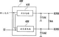
图3是示出DC-DC转换器的实施例的示意图。参照图3,DC-DC转换器400a包括升压电路410a、逆变器电路420a、电容器Cch以及具有Rch和Mch的开关单元。FIG. 3 is a schematic diagram illustrating an embodiment of a DC-DC converter. Referring to FIG. 3, the DC-
升压电路410a是用于接收输入电压并被构造为对输入电压进行升压以产生第一电压ELVDD的装置。例如,输入电压可以来自于移动电话的电池等。The
逆变器电路420a是用于接收输入电压并被构造为对输入电压进行逆变以产生具有低电压的第二电压ELVSS的装置。The
此外,升压电路410a和逆变器电路420a接收控制信号CS,其中,控制信号CS控制是否操作升压电路410a和逆变器电路420a。In addition, the
电容器Cch连接到DC-DC转换器400a的输出第一电压ELVDD的输出端,从而能够使DC-DC转换器400a稳定地进行输出。The capacitor Cch is connected to an output terminal of the DC-
在该实施例中,具有Rch和Mch的开关单元位于DC-DC转换器400a内部,并连接到电容器Cch,且被构造为根据控制信号CS释放充在电容器Cch中的电压或保持充在电容器Cch中的电压。In this embodiment, a switch unit having Rch and Mch is located inside the DC-
通过控制信号CS来使升压电路410a停止,电容器Cch充有第一电源ELVDD的电压。因此,通过所充有的电压将第一电源ELVDD的电压发送到图2中示出的像素单元,使得像素单元的各像素接收第一电压ELVDD。像素在升压电路410a的操作停止时发生不期望的发光,从而缩短了像素的寿命。The
因此,为了防止这种不期望的发光,具有Rch和Mch的开关单元连接到电容器Cch,以产生释放存储在电容器Cch中的电压的通路。Therefore, in order to prevent such undesired light emission, the switching unit having Rch and Mch is connected to the capacitor Cch to create a path for discharging the voltage stored in the capacitor Cch.
开关单元包括电阻器Rch和晶体管Mch。在该实施例中,电阻器Rch的一端连接到升压电路410a的输出端,另一端连接到晶体管Mch的源极。晶体管Mch的源极连接到电阻器Rch,晶体管Mch的漏极连接到输出从逆变器电路420a产生的第二电压ELVSS的输出端,晶体管Mch的栅极接收控制信号CS,其中,控制信号CS操作DC-DC转换器400a以实施开关操作。在一些实施例中,电阻器Rch可以连接到第二电压ELVSS,晶体管Mch可以连接到升压电路410a的输出端。The switch unit includes a resistor Rch and a transistor Mch. In this embodiment, one end of the resistor Rch is connected to the output end of the
当通过控制信号CS操作DC-DC转换器400a时,晶体管Mch处于截止状态,当停止操作DC-DC转换器400a时,晶体管Mch处于导通状态。因此,当晶体管Mch处于导通状态时,第二电压ELVSS被发送到电阻器Rch的一端,以使得存储在电容器Cch中的电压通过电阻器Rch流入第二电源ELVSS,从而通过电阻器Rch来传导存储在电容器Cch中的电荷。当晶体管Mch处于截止状态时,电流没有流入电阻器Rch,从而基本不对升压电路410a的输出端的电压造成影响。The transistor Mch is in an off state when the DC-
因此,当DC-DC转换器400a处于截止状态时,在电容器Cch中充有的电压被释放。结果,当DC-DC转换器400a处于截止状态时,开关单元防止第一电压ELVDD被传输到图2的像素单元,从而可以防止像素单元的各像素发光。Therefore, when the DC-
图4是示出DC-DC转换器的另一实施例的示意图。参照图4,DC-DC转换器400b包括升压电路410b、逆变器电路420b、电容器Cch和开关单元Rch及Mch。Fig. 4 is a schematic diagram showing another embodiment of a DC-DC converter. Referring to FIG. 4, the DC-
与图3中示出的DC-DC转换器400a不同的是,在图4中示出的DC-DC转换器400b中,开关单元Rch及Mch的晶体管Mch的一端没有连接到逆变器电路420b的输出端,而是连接到地。因此,当根据控制信号CS停止升压电路410b时,存储在电容器Cch中的电荷通过晶体管Mch流入地。Unlike the DC-
因此,当DC-DC转换器400b处于截止状态时,在电容器Cch中充有的电压被释放。结果,当DC-DC转换器400b处于截止状态时,开关单元防止第一电压ELVDD在预定时间内被发送到图2的像素单元,从而可以防止像素单元的各像素发光。Therefore, when the DC-
图5是示出DC-DC转换器的另一实施例的示意图。参照图5,DC-DC转换器400c包括升压电路410c和逆变器电路420c,DC-DC转换器400c的输出端连接到电容器Cch和开关单元Mch。Fig. 5 is a schematic diagram showing another embodiment of a DC-DC converter. Referring to FIG. 5, the DC-DC converter 400c includes a
图5中示出的DC-DC转换器400c与图3中示出的DC-DC转换器400a之间的区别在于,晶体管Mch连接到DC-DC转换器400c外部的输出信号。The difference between the DC-DC converter 400c shown in FIG. 5 and the DC-
晶体管Mch的源极连接到第一电源ELVDD的输出端,晶体管Mch的漏极连接到地。The source of the transistor Mch is connected to the output terminal of the first power supply ELVDD, and the drain of the transistor Mch is connected to the ground.
因此,当根据控制信号CS停止升压电路410c时,存储在电容器Cch中的电压通过晶体管Mch流入地。Therefore, when the boosting
因此,当DC-DC转换器400c处于截止状态时,在电容器Cch中充有的电压被释放。结果,当DC-DC转换器400c处于截止状态时,晶体管Mch防止第一电压ELVDD被发送到图2的像素单元,从而可以防止像素单元的各像素发光。Therefore, when the DC-DC converter 400c is in the OFF state, the voltage charged in the capacitor Cch is discharged. As a result, when the DC-DC converter 400c is in an off state, the transistor Mch prevents the first voltage ELVDD from being transmitted to the pixel unit of FIG. 2 , so that each pixel of the pixel unit may be prevented from emitting light.
图6是示出DC-DC转换器的另一实施例的示意图。参照图6,DC-DC转换器400d包括升压电路410d和逆变器电路420d,DC-DC转换器400d的输出端连接到电容器Cch和开关单元,延迟电路430连接在控制信号CS的输入端与开关单元之间。Fig. 6 is a schematic diagram showing another embodiment of a DC-DC converter. 6, the DC-DC converter 400d includes a
升压电路410d是用于对输入电压进行升压以产生第一电压ELVDD的装置。例如,可以从移动电话的电池等发送输入电压。The
逆变器电路420d是用于对输入电压进行逆变以产生第二电压ELVSS的装置。The
升压电路410d和逆变器电路420d接收控制信号CS以确定升压电路410d和逆变器电路420d是否被操作。The
电容器Cch连接到DC-DC转换器400d的输出端,从而可以使DC-DC转换器400d稳定地进行输出。The capacitor Cch is connected to the output terminal of the DC-DC converter 400d, so that the output of the DC-DC converter 400d can be stabilized.
开关单元形成在DC-DC转换器400d的外部,并释放在电容器Cch中充有的电压。当在电容器Cch中充有的电压没有被释放,且DC-DC转换器400d在其操作过程中停止时,电容器Cch充有第一电源ELVDD的电压。因此,第一电源ELVDD的电压通过电容器Cch中充有的电压被传输到图2中示出的像素单元,使得像素单元的各像素接收第一电压ELVDD并会发射不期望的光。像素的这种发光缩短了像素的寿命。因此,为了防止这种发光,产生了用于由开关单元将存储在电容器Cch中的电压释放的通路。开关单元包括晶体管Mch。晶体管Mch的源极连接到升压电路410d的输出端,晶体管Mch的漏极连接到地,晶体管Mch的栅极接收控制信号CS,其中,控制信号CS操作DC-DC转换器400d以实施开关操作。换言之,当通过控制信号CS操作DC-DC转换器400d时,晶体管Mch处于截止状态,当停止操作DC-DC转换器400d时,晶体管Mch处于导通状态。当晶体管Mch处于导通状态时,存储在电容器Cch中的电荷通过晶体管Mch流入地,以释放存储在电容器Cch中的电压。当晶体管Mch处于截止状态时,电流没有流动,从而基本不对升压电路410d的输出端的电压造成影响。The switching unit is formed outside the DC-DC converter 400d, and discharges the voltage charged in the capacitor Cch. When the voltage charged in the capacitor Cch is not discharged, and the DC-DC converter 400d is stopped during its operation, the capacitor Cch is charged with the voltage of the first power source ELVDD. Accordingly, the voltage of the first power source ELVDD is transferred to the pixel unit shown in FIG. 2 through the voltage charged in the capacitor Cch, so that each pixel of the pixel unit receives the first voltage ELVDD and may emit undesired light. This light emission of the pixel shortens the lifetime of the pixel. Therefore, in order to prevent such light emission, a path for discharging the voltage stored in the capacitor Cch by the switching unit is created. The switching unit includes a transistor Mch. The source of the transistor Mch is connected to the output terminal of the
换言之,当DC-DC转换器400d处于截止状态时,在电容器Cch中充有的电压被释放。结果,当DC-DC转换器400d处于截止状态时,开关单元防止第一电压ELVDD被传输到图2的像素单元,从而可以防止像素单元的各像素发光。In other words, when the DC-DC converter 400d is in the off state, the voltage charged in the capacitor Cch is discharged. As a result, when the DC-DC converter 400d is in an off state, the switching unit prevents the first voltage ELVDD from being transmitted to the pixel unit of FIG. 2 , so that each pixel of the pixel unit may be prevented from emitting light.
延迟电路430是用于延迟将控制信号CS施加到晶体管Mch的装置。在DC-DC转换器400d被停止之后,延迟电路430延迟导通晶体管Mch。因此,电容器Cch中的电荷在停止操作DC-DC转换器400d之后没有立即通过晶体管Mch流入地,而是在延迟之后通过晶体管Mch流入地,从而没有立即阻断第一电源ELVDD。The
图7是示出DC-DC转换器的另一实施例的结构图。参照图7,DC-DC转换器400e包括升压电路410e和逆变器电路420e,DC-DC转换器400e的输出端连接到电容器Cch和电阻器Rch。FIG. 7 is a block diagram showing another embodiment of the DC-DC converter. Referring to FIG. 7, the DC-
升压电路410e是用于对输入电压进行升压以产生第一电压ELVDD的装置。例如,可以从移动电话的电池等发送输入电压。The
逆变器电路420e是用于对输入电压进行逆变以产生第二电压ELVSS的装置。The
升压电路410e和逆变器电路420e接收控制信号CS,以确定升压电路410e和逆变器电路420e是否被操作。The
电容器Cch连接到DC-DC转换器400e的输出端,从而可以使DC-DC转换器400e稳定地进行输出。The capacitor Cch is connected to the output terminal of the DC-
在该实施例中,电阻器Rch形成在DC-DC转换器400e的外部,并释放电容器Cch中的电荷。当电容器Cch中充有的电压没有被释放,且DC-DC转换器400e在其操作过程中被停止时,电容器Cch充有第一电源ELVDD的电压。因此,第一电源ELVDD的电压通过升压电路410e被传输到图2中示出的像素单元,使得像素单元的各像素接收第一电压ELVDD并可发光。像素在DC-DC转换器400e的操作被停止的情况下发生的发光对像素的寿命等具有不利的影响。因此,为了防止这种发光,产生了通过电阻器Rch使电容器Cch放电的通路。电阻器Rch的一端连接到DC-DC转换器400e的输出端,电阻器Rch的另一端连接到地。因此,在电容器Cch中充有的电压通过电阻器Rch被释放。由于电容器Cch中充有的电压的释放时间对应于电容器Cch的大小以及电阻器Rch的大小,因此控制电容器Cch和电阻器Rch的大小,从而防止电容器Cch中充有的电压被释放得太快或太慢。In this embodiment, the resistor Rch is formed outside the DC-
由于在DC-DC转换器400e处于截止状态之后释放存储在DC-DC转换器400e的输出端处的电压,所以防止了第一电源ELVDD的电压被传输到图2的像素单元,从而可以防止像素单元的各像素发光。Since the voltage stored at the output terminal of the DC-
图8是示出DC-DC转换器的另一实施例的结构图。参照图8,DC-DC转换器400f包括升压电路410f和逆变器电路420f,DC-DC转换器400f的输出端连接到电容器Cch1和Cch2以及电阻器Rch。FIG. 8 is a block diagram showing another embodiment of the DC-DC converter. 8, the DC-
升压电路410f是用于对输入电压进行升压以产生第一电压ELVDD的装置。例如,可以从移动电话的电池等传输输入电压。The
逆变器电路420f是用于对输入电压进行逆变以产生第二电压ELVSS的装置。The
升压电路410f和逆变器电路420f接收控制信号CS以确定升压电路410f和逆变器电路420f是否被操作。The
电容器Cch1和Cch2分别连接到升压电路410f和逆变器电路420f的输出端,从而可以稳定地输出第一电源ELVDD的电压和第二电源ELVSS的电压。Capacitors Cch1 and Cch2 are respectively connected to the output terminals of the boosting
电阻器Rch形成在DC-DC转换器400f的外部,且释放在电容器Cch1和Cch2中充有的电压。当电容器Cch1和Cch2中充有的电压没有被释放,且DC-DC转换器400f在其操作过程中被停止时,电容器Cch1和Cch2分别充有第一电源ELVDD的电压和第二电源ELVSS的电压。因此,第一电源ELVDD的电压和第二电源ELVSS的电压被发送到图2中示出的像素单元,从而像素单元的各像素可发光。像素在DC-DC转换器400f的操作被停止的情况下产生的发光对像素的寿命等具有不利的影响。因此,为了防止这种发光,产生了通过电阻器Rch释放电容器Cch1和Cch2中存储的电压的通路。电阻器Rch的一端连接到升压电路410f的输出端,电阻器Rch的另一端连接到逆变器电路420f的输出端。因此,电阻器Rch位于第一电源ELVDD的电压与第二电源ELVSS的电压之间,以使电容器Cch1和Cch2放电。由于电容器Cch1和Cch2中充有的电压的释放时间对应于电容器Cch1和Cch2的大小以及电阻器Rch的大小,因此控制电容器Cch1和Cch2以及电阻器Rch的大小,从而防止电容器Cch1和Cch2中充有的电压被释放得太快或太慢。The resistor Rch is formed outside the DC-
由于在DC-DC转换器400f处于截止状态之后释放存储在DC-DC转换器400f的输出端中的电压,所以防止了将存储在DC-DC转换器400f的输出端中的电压传输到图2的像素单元,从而可以防止像素单元的各像素发光。Since the voltage stored in the output terminal of the DC-
采用根据本发明的DC-DC转换器以及利用该DC-DC转换器的有机发光显示器,可以防止DC-DC转换器截止时由于将第一电压ELVDD和第二电压ELVSS施加到像素而导致的不利的发光现象。With the DC-DC converter and the organic light emitting display using the DC-DC converter according to the present invention, it is possible to prevent disadvantages caused by applying the first voltage ELVDD and the second voltage ELVSS to the pixels when the DC-DC converter is turned off. luminescence phenomenon.
虽然示出并描述了本发明的特定实施例,但是本领域技术人员应该理解,在不脱离本发明的原理和精神的情况下,可以对该实施例作出修改。While a particular embodiment of the present invention has been shown and described, it will be understood by those skilled in the art that modifications may be made to that embodiment without departing from the principles and spirit of the invention.
Claims (20)
Applications Claiming Priority (2)
| Application Number | Priority Date | Filing Date | Title |
|---|---|---|---|
| KR1020070086511AKR100889690B1 (en) | 2007-08-28 | 2007-08-28 | DC-DC converter and organic light emitting display device using the same |
| KR1020070086511 | 2007-08-28 |
Publications (1)
| Publication Number | Publication Date |
|---|---|
| CN101378229Atrue CN101378229A (en) | 2009-03-04 |
Family
ID=40092049
Family Applications (1)
| Application Number | Title | Priority Date | Filing Date |
|---|---|---|---|
| CNA2008102124427APendingCN101378229A (en) | 2007-08-28 | 2008-08-26 | DC-DC converter and organic light emitting display using the same |
Country Status (5)
| Country | Link |
|---|---|
| US (1) | US8749462B2 (en) |
| EP (1) | EP2031941A3 (en) |
| JP (1) | JP4659807B2 (en) |
| KR (1) | KR100889690B1 (en) |
| CN (1) | CN101378229A (en) |
Cited By (2)
| Publication number | Priority date | Publication date | Assignee | Title |
|---|---|---|---|---|
| CN105657898A (en)* | 2016-02-19 | 2016-06-08 | 京东方科技集团股份有限公司 | Power supply circuit and drive method thereof and display device |
| US9799298B2 (en) | 2010-04-23 | 2017-10-24 | Semiconductor Energy Laboratory Co., Ltd. | Liquid crystal display device and driving method thereof |
Families Citing this family (21)
| Publication number | Priority date | Publication date | Assignee | Title |
|---|---|---|---|---|
| JP4502003B2 (en)* | 2007-12-26 | 2010-07-14 | エプソンイメージングデバイス株式会社 | Electro-optical device and electronic apparatus including the electro-optical device |
| KR100952834B1 (en)* | 2008-08-06 | 2010-04-15 | 삼성모바일디스플레이주식회사 | DC-DC converter and organic light emitting display device using the same |
| JP5515331B2 (en) | 2009-03-09 | 2014-06-11 | ソニー株式会社 | Information providing server, information providing system, information providing method, and program |
| KR101049019B1 (en)* | 2009-05-19 | 2011-07-12 | 삼성모바일디스플레이주식회사 | Power supply unit and organic light emitting display device using the same |
| KR101067225B1 (en)* | 2009-07-08 | 2011-09-22 | 삼성전기주식회사 | On / off sequence circuit for plasma display panel |
| KR101022085B1 (en) | 2009-07-10 | 2011-03-17 | 삼성모바일디스플레이주식회사 | Power supply unit and organic light emitting display device using the same |
| KR101084170B1 (en)* | 2009-08-03 | 2011-11-17 | 삼성모바일디스플레이주식회사 | Power control system for external display module of DC-DC converter |
| KR101040798B1 (en)* | 2009-11-17 | 2011-06-14 | 삼성모바일디스플레이주식회사 | DC-DC converter and organic light emitting display device using the same |
| KR101064462B1 (en)* | 2009-11-17 | 2011-09-15 | 삼성모바일디스플레이주식회사 | DC-DC converter and organic light emitting display device using the same |
| KR101132023B1 (en) | 2010-02-19 | 2012-04-02 | 삼성모바일디스플레이주식회사 | Dc-dc converter and organic light emitting display using the same |
| KR101193194B1 (en)* | 2010-04-30 | 2012-10-19 | 삼성디스플레이 주식회사 | Organic Light Emitting Display |
| KR101992281B1 (en)* | 2012-03-06 | 2019-06-26 | 삼성디스플레이 주식회사 | Organic Light Emitting Display and Driving Method Thereof |
| KR101975531B1 (en)* | 2012-09-10 | 2019-05-08 | 삼성디스플레이 주식회사 | Organic Light Emitting Display Device and Driving Method Thereof |
| KR102071004B1 (en) | 2013-09-03 | 2020-01-30 | 삼성디스플레이 주식회사 | Dc-dc converter and organic light emitting display including the same |
| KR102141207B1 (en)* | 2013-11-11 | 2020-08-05 | 삼성디스플레이 주식회사 | Display apparatus, power voltage generating apparatus, and method for generating power voltage |
| KR102395148B1 (en)* | 2015-03-03 | 2022-05-09 | 삼성디스플레이 주식회사 | Dc-dc converter and display device having the same |
| KR102484869B1 (en)* | 2015-12-02 | 2023-01-06 | 엘지디스플레이 주식회사 | Organic light emitting display device and method for driving organic light emitting display device |
| KR102430795B1 (en)* | 2015-12-31 | 2022-08-08 | 엘지디스플레이 주식회사 | Display device and method for driving the same |
| CN107103871B (en)* | 2017-06-30 | 2019-11-22 | 京东方科技集团股份有限公司 | Display device, power supply circuit and power supply method of display screen |
| CN110544452B (en)* | 2018-05-28 | 2021-08-17 | 京东方科技集团股份有限公司 | Power supply timing control circuit and control method, display drive circuit, and display device |
| KR102519570B1 (en) | 2018-11-12 | 2023-04-10 | 삼성디스플레이 주식회사 | Display apparatus and method of driving display panel using the same |
Family Cites Families (23)
| Publication number | Priority date | Publication date | Assignee | Title |
|---|---|---|---|---|
| US4422073A (en)* | 1981-10-27 | 1983-12-20 | The Bendix Corporation | Combustible gas detection system |
| CN1023048C (en) | 1989-08-17 | 1993-12-08 | 哈尔滨工业大学 | Phase-and width-discriminating phase-failure protector |
| JPH05236744A (en)* | 1992-02-19 | 1993-09-10 | Ricoh Co Ltd | Multi-output switching power supply |
| JP2000152623A (en) | 1998-11-10 | 2000-05-30 | Ricoh Co Ltd | Power supply |
| GB9921425D0 (en) | 1999-09-11 | 1999-11-10 | Koninkl Philips Electronics Nv | Active matrix electroluminescent display device |
| KR100389019B1 (en)* | 2000-11-22 | 2003-06-25 | 엘지전자 주식회사 | Reset Circuit in Plasma Display Panel |
| JP2002233139A (en) | 2001-02-05 | 2002-08-16 | Matsushita Electric Ind Co Ltd | DC-DC converter |
| JP2002244617A (en)* | 2001-02-15 | 2002-08-30 | Sanyo Electric Co Ltd | Organic el pixel circuit |
| JP3788916B2 (en) | 2001-03-30 | 2006-06-21 | 株式会社日立製作所 | Light-emitting display device |
| KR100878222B1 (en) | 2001-07-03 | 2009-01-13 | 삼성전자주식회사 | Power Supply for Liquid Crystal Display |
| US7483001B2 (en) | 2001-11-21 | 2009-01-27 | Seiko Epson Corporation | Active matrix substrate, electro-optical device, and electronic device |
| US7698573B2 (en)* | 2002-04-02 | 2010-04-13 | Sharp Corporation | Power source apparatus for display and image display apparatus |
| KR100514185B1 (en)* | 2003-10-01 | 2005-09-13 | 삼성에스디아이 주식회사 | DC-DC Converter for electro luminescence display |
| US6913554B2 (en)* | 2003-10-03 | 2005-07-05 | Gilbert W. Younger | Methods and systems for improving the operation of transmissions for motor vehicles |
| KR20050046927A (en)* | 2003-11-14 | 2005-05-19 | 삼성에스디아이 주식회사 | Power supply and light emitting display device using the power supply |
| GB0400213D0 (en) | 2004-01-07 | 2004-02-11 | Koninkl Philips Electronics Nv | Electroluminescent display devices |
| JP4803629B2 (en)* | 2004-04-27 | 2011-10-26 | 東北パイオニア株式会社 | Light emitting display device and drive control method thereof |
| KR100662981B1 (en)* | 2004-11-04 | 2006-12-28 | 삼성에스디아이 주식회사 | LED display and its DC-DC converter |
| CN100486089C (en) | 2004-12-25 | 2009-05-06 | 鸿富锦精密工业(深圳)有限公司 | Switching power supply |
| JP4984391B2 (en)* | 2005-01-07 | 2012-07-25 | カシオ計算機株式会社 | Display drive device, display device, and drive control method thereof |
| KR100649508B1 (en)* | 2005-02-02 | 2006-11-27 | 권오영 | Hybrid power system |
| KR101152118B1 (en) | 2005-02-16 | 2012-06-15 | 삼성전자주식회사 | Driving apparatus of display device and dc-dc converter |
| KR20080064564A (en)* | 2007-01-05 | 2008-07-09 | 삼성전자주식회사 | Printed circuit board and liquid crystal display device comprising the same |
- 2007
- 2007-08-28KRKR1020070086511Apatent/KR100889690B1/enactiveActive
- 2007-10-23JPJP2007275362Apatent/JP4659807B2/ennot_activeExpired - Fee Related
- 2008
- 2008-07-08USUS12/217,817patent/US8749462B2/enactiveActive
- 2008-08-26CNCNA2008102124427Apatent/CN101378229A/enactivePending
- 2008-08-27EPEP08163107Apatent/EP2031941A3/ennot_activeWithdrawn
Cited By (3)
| Publication number | Priority date | Publication date | Assignee | Title |
|---|---|---|---|---|
| US9799298B2 (en) | 2010-04-23 | 2017-10-24 | Semiconductor Energy Laboratory Co., Ltd. | Liquid crystal display device and driving method thereof |
| CN105657898A (en)* | 2016-02-19 | 2016-06-08 | 京东方科技集团股份有限公司 | Power supply circuit and drive method thereof and display device |
| US10140917B2 (en) | 2016-02-19 | 2018-11-27 | Boe Technology Group Co., Ltd. | Power supply circuit, driving method for the same and display device |
Also Published As
| Publication number | Publication date |
|---|---|
| US8749462B2 (en) | 2014-06-10 |
| KR100889690B1 (en) | 2009-03-19 |
| JP2009055774A (en) | 2009-03-12 |
| US20090058311A1 (en) | 2009-03-05 |
| EP2031941A3 (en) | 2012-01-11 |
| KR20090021742A (en) | 2009-03-04 |
| JP4659807B2 (en) | 2011-03-30 |
| EP2031941A2 (en) | 2009-03-04 |
Similar Documents
| Publication | Publication Date | Title |
|---|---|---|
| CN101378229A (en) | DC-DC converter and organic light emitting display using the same | |
| US9041626B2 (en) | Organic light emitting display and power supply method thereof | |
| US8482492B2 (en) | Organic light emitting display with an improved emission control driver and method of driving the same | |
| KR101056289B1 (en) | DC-DC converter and organic light emitting display device using the same | |
| CN101393721B (en) | Pixel driving method and apparatus for organic light emitting device | |
| KR101829398B1 (en) | Organic Light Emitting Display and Driving Method Thereof | |
| CN101533851B (en) | Pixel and organic light emitting display using same | |
| EP2151816B1 (en) | Organic light emitting display device and power supply arrangement for the same | |
| US8665182B2 (en) | Emission control driver and organic light emitting display device using the same | |
| US8411077B2 (en) | DC-DC converter and organic light emitting display device using the same | |
| CN104008722B (en) | Organic light emitting display | |
| US20100039423A1 (en) | Scan driver and organic light emitting display using the same | |
| US20100128021A1 (en) | Pixel and organic light emitting display device using the same | |
| US9207785B2 (en) | Voltage generator and organic light emitting display device using the same | |
| CN101520983B (en) | Organic light emitting display and driving method thereof | |
| CN101819749A (en) | Power supply unit and organic light emitting display device using the same | |
| KR102012925B1 (en) | Organic Light Emitting Display Device and Driving Method thereof | |
| US9508288B2 (en) | Organic light emitting display device and method of driving the same | |
| KR100916906B1 (en) | Buffer and organic light emitting display using the same | |
| CN101206825A (en) | Pixel, display using the pixel and driving method thereof | |
| KR100520829B1 (en) | Driving Apparatus And Method For Electro-Luminescence Display Panel |
Legal Events
| Date | Code | Title | Description |
|---|---|---|---|
| C06 | Publication | ||
| C41 | Transfer of patent application or patent right or utility model | ||
| PB01 | Publication | ||
| TA01 | Transfer of patent application right | Effective date of registration:20090116 Address after:Gyeonggi Do Korea Suwon Applicant after:Samsung Mobile Display Co., Ltd. Address before:Gyeonggi Do Korea Suwon Applicant before:Samsung SDI Co., Ltd. | |
| ASS | Succession or assignment of patent right | Owner name:SAMSUNG MOBILE DISPLAY CO., LTD. Free format text:FORMER OWNER: SAMSUNG SDI CO., LTD. Effective date:20090116 | |
| C10 | Entry into substantive examination | ||
| SE01 | Entry into force of request for substantive examination | ||
| ASS | Succession or assignment of patent right | Owner name:SAMSUNG DISPLAY CO., LTD. Free format text:FORMER OWNER: SAMSUNG MOBILE DISPLAY CO., LTD. Effective date:20121119 | |
| C41 | Transfer of patent application or patent right or utility model | ||
| TA01 | Transfer of patent application right | Effective date of registration:20121119 Address after:South Korea Gyeonggi Do Yongin Applicant after:Samsung Display Co., Ltd. Address before:Gyeonggi Do Korea Suwon Applicant before:Samsung Mobile Display Co., Ltd. | |
| C12 | Rejection of a patent application after its publication | ||
| RJ01 | Rejection of invention patent application after publication | Application publication date:20090304 |