CN101378023B - Semiconductor package and fabrication method thereof - Google Patents
Semiconductor package and fabrication method thereofDownload PDFInfo
- Publication number
- CN101378023B CN101378023BCN2007101477234ACN200710147723ACN101378023BCN 101378023 BCN101378023 BCN 101378023BCN 2007101477234 ACN2007101477234 ACN 2007101477234ACN 200710147723 ACN200710147723 ACN 200710147723ACN 101378023 BCN101378023 BCN 101378023B
- Authority
- CN
- China
- Prior art keywords
- chip
- semiconductor package
- pad
- carrier board
- connection
- Prior art date
- Legal status (The legal status is an assumption and is not a legal conclusion. Google has not performed a legal analysis and makes no representation as to the accuracy of the status listed.)
- Expired - Fee Related
Links
- 239000004065semiconductorSubstances0.000titleclaimsabstractdescription86
- 238000000034methodMethods0.000titleclaimsabstractdescription21
- 238000004519manufacturing processMethods0.000titleclaimsdescription49
- 238000005538encapsulationMethods0.000claimsabstractdescription16
- 150000001875compoundsChemical class0.000claimsabstractdescription12
- 239000000084colloidal systemSubstances0.000claimsabstractdescription8
- 238000004806packaging method and processMethods0.000claimsdescription21
- 229910000679solderInorganic materials0.000claimsdescription21
- 239000008393encapsulating agentSubstances0.000claimsdescription10
- 238000003466weldingMethods0.000claimsdescription10
- 230000002940repellentEffects0.000claimsdescription7
- 239000005871repellentSubstances0.000claimsdescription7
- 230000001846repelling effectEffects0.000claimsdescription4
- 238000000465mouldingMethods0.000abstractdescription9
- 238000000926separation methodMethods0.000abstractdescription7
- 230000003647oxidationEffects0.000abstractdescription2
- 238000007254oxidation reactionMethods0.000abstractdescription2
- 230000009545invasionEffects0.000abstract1
- 239000000758substrateSubstances0.000description20
- 238000010586diagramMethods0.000description15
- 239000003292glueSubstances0.000description12
- 239000000463materialSubstances0.000description5
- PXHVJJICTQNCMI-UHFFFAOYSA-NNickelChemical compound[Ni]PXHVJJICTQNCMI-UHFFFAOYSA-N0.000description3
- 239000011248coating agentSubstances0.000description3
- 238000000576coating methodMethods0.000description3
- 238000005530etchingMethods0.000description3
- 239000010931goldSubstances0.000description3
- ABJSOROVZZKJGI-OCYUSGCXSA-N(1r,2r,4r)-2-(4-bromophenyl)-n-[(4-chlorophenyl)-(2-fluoropyridin-4-yl)methyl]-4-morpholin-4-ylcyclohexane-1-carboxamideChemical compoundC1=NC(F)=CC(C(NC(=O)[C@H]2[C@@H](C[C@@H](CC2)N2CCOCC2)C=2C=CC(Br)=CC=2)C=2C=CC(Cl)=CC=2)=C1ABJSOROVZZKJGI-OCYUSGCXSA-N0.000description2
- 238000005520cutting processMethods0.000description2
- 230000006870functionEffects0.000description2
- 239000002184metalSubstances0.000description2
- 229910052751metalInorganic materials0.000description2
- 238000009736wettingMethods0.000description2
- GLGNXYJARSMNGJ-VKTIVEEGSA-N(1s,2s,3r,4r)-3-[[5-chloro-2-[(1-ethyl-6-methoxy-2-oxo-4,5-dihydro-3h-1-benzazepin-7-yl)amino]pyrimidin-4-yl]amino]bicyclo[2.2.1]hept-5-ene-2-carboxamideChemical compoundCCN1C(=O)CCCC2=C(OC)C(NC=3N=C(C(=CN=3)Cl)N[C@H]3[C@H]([C@@]4([H])C[C@@]3(C=C4)[H])C(N)=O)=CC=C21GLGNXYJARSMNGJ-VKTIVEEGSA-N0.000description1
- QBWKPGNFQQJGFY-QLFBSQMISA-N3-[(1r)-1-[(2r,6s)-2,6-dimethylmorpholin-4-yl]ethyl]-n-[6-methyl-3-(1h-pyrazol-4-yl)imidazo[1,2-a]pyrazin-8-yl]-1,2-thiazol-5-amineChemical compoundN1([C@H](C)C2=NSC(NC=3C4=NC=C(N4C=C(C)N=3)C3=CNN=C3)=C2)C[C@H](C)O[C@H](C)C1QBWKPGNFQQJGFY-QLFBSQMISA-N0.000description1
- RYGMFSIKBFXOCR-UHFFFAOYSA-NCopperChemical compound[Cu]RYGMFSIKBFXOCR-UHFFFAOYSA-N0.000description1
- BQCADISMDOOEFD-UHFFFAOYSA-NSilverChemical compound[Ag]BQCADISMDOOEFD-UHFFFAOYSA-N0.000description1
- 229940125758compound 15Drugs0.000description1
- 229940125846compound 25Drugs0.000description1
- 229910052802copperInorganic materials0.000description1
- 239000010949copperSubstances0.000description1
- 230000000694effectsEffects0.000description1
- 238000005516engineering processMethods0.000description1
- 229910052737goldInorganic materials0.000description1
- 238000012986modificationMethods0.000description1
- 230000004048modificationEffects0.000description1
- 229910052759nickelInorganic materials0.000description1
- 238000012858packaging processMethods0.000description1
- 239000011347resinSubstances0.000description1
- 229920005989resinPolymers0.000description1
- 230000036299sexual functionEffects0.000description1
- 229910052709silverInorganic materials0.000description1
- 239000004332silverSubstances0.000description1
- 238000005476solderingMethods0.000description1
- 230000008646thermal stressEffects0.000description1
Images


Classifications
- H—ELECTRICITY
- H01—ELECTRIC ELEMENTS
- H01L—SEMICONDUCTOR DEVICES NOT COVERED BY CLASS H10
- H01L2224/00—Indexing scheme for arrangements for connecting or disconnecting semiconductor or solid-state bodies and methods related thereto as covered by H01L24/00
- H01L2224/01—Means for bonding being attached to, or being formed on, the surface to be connected, e.g. chip-to-package, die-attach, "first-level" interconnects; Manufacturing methods related thereto
- H01L2224/26—Layer connectors, e.g. plate connectors, solder or adhesive layers; Manufacturing methods related thereto
- H01L2224/31—Structure, shape, material or disposition of the layer connectors after the connecting process
- H01L2224/32—Structure, shape, material or disposition of the layer connectors after the connecting process of an individual layer connector
- H01L2224/321—Disposition
- H01L2224/32151—Disposition the layer connector connecting between a semiconductor or solid-state body and an item not being a semiconductor or solid-state body, e.g. chip-to-substrate, chip-to-passive
- H01L2224/32221—Disposition the layer connector connecting between a semiconductor or solid-state body and an item not being a semiconductor or solid-state body, e.g. chip-to-substrate, chip-to-passive the body and the item being stacked
- H01L2224/32245—Disposition the layer connector connecting between a semiconductor or solid-state body and an item not being a semiconductor or solid-state body, e.g. chip-to-substrate, chip-to-passive the body and the item being stacked the item being metallic
- H—ELECTRICITY
- H01—ELECTRIC ELEMENTS
- H01L—SEMICONDUCTOR DEVICES NOT COVERED BY CLASS H10
- H01L2224/00—Indexing scheme for arrangements for connecting or disconnecting semiconductor or solid-state bodies and methods related thereto as covered by H01L24/00
- H01L2224/01—Means for bonding being attached to, or being formed on, the surface to be connected, e.g. chip-to-package, die-attach, "first-level" interconnects; Manufacturing methods related thereto
- H01L2224/42—Wire connectors; Manufacturing methods related thereto
- H01L2224/47—Structure, shape, material or disposition of the wire connectors after the connecting process
- H01L2224/48—Structure, shape, material or disposition of the wire connectors after the connecting process of an individual wire connector
- H01L2224/4805—Shape
- H01L2224/4809—Loop shape
- H01L2224/48091—Arched
- H—ELECTRICITY
- H01—ELECTRIC ELEMENTS
- H01L—SEMICONDUCTOR DEVICES NOT COVERED BY CLASS H10
- H01L2224/00—Indexing scheme for arrangements for connecting or disconnecting semiconductor or solid-state bodies and methods related thereto as covered by H01L24/00
- H01L2224/01—Means for bonding being attached to, or being formed on, the surface to be connected, e.g. chip-to-package, die-attach, "first-level" interconnects; Manufacturing methods related thereto
- H01L2224/42—Wire connectors; Manufacturing methods related thereto
- H01L2224/47—Structure, shape, material or disposition of the wire connectors after the connecting process
- H01L2224/48—Structure, shape, material or disposition of the wire connectors after the connecting process of an individual wire connector
- H01L2224/481—Disposition
- H01L2224/48151—Connecting between a semiconductor or solid-state body and an item not being a semiconductor or solid-state body, e.g. chip-to-substrate, chip-to-passive
- H01L2224/48221—Connecting between a semiconductor or solid-state body and an item not being a semiconductor or solid-state body, e.g. chip-to-substrate, chip-to-passive the body and the item being stacked
- H01L2224/48225—Connecting between a semiconductor or solid-state body and an item not being a semiconductor or solid-state body, e.g. chip-to-substrate, chip-to-passive the body and the item being stacked the item being non-metallic, e.g. insulating substrate with or without metallisation
- H01L2224/48227—Connecting between a semiconductor or solid-state body and an item not being a semiconductor or solid-state body, e.g. chip-to-substrate, chip-to-passive the body and the item being stacked the item being non-metallic, e.g. insulating substrate with or without metallisation connecting the wire to a bond pad of the item
- H—ELECTRICITY
- H01—ELECTRIC ELEMENTS
- H01L—SEMICONDUCTOR DEVICES NOT COVERED BY CLASS H10
- H01L2224/00—Indexing scheme for arrangements for connecting or disconnecting semiconductor or solid-state bodies and methods related thereto as covered by H01L24/00
- H01L2224/01—Means for bonding being attached to, or being formed on, the surface to be connected, e.g. chip-to-package, die-attach, "first-level" interconnects; Manufacturing methods related thereto
- H01L2224/42—Wire connectors; Manufacturing methods related thereto
- H01L2224/47—Structure, shape, material or disposition of the wire connectors after the connecting process
- H01L2224/48—Structure, shape, material or disposition of the wire connectors after the connecting process of an individual wire connector
- H01L2224/481—Disposition
- H01L2224/48151—Connecting between a semiconductor or solid-state body and an item not being a semiconductor or solid-state body, e.g. chip-to-substrate, chip-to-passive
- H01L2224/48221—Connecting between a semiconductor or solid-state body and an item not being a semiconductor or solid-state body, e.g. chip-to-substrate, chip-to-passive the body and the item being stacked
- H01L2224/48245—Connecting between a semiconductor or solid-state body and an item not being a semiconductor or solid-state body, e.g. chip-to-substrate, chip-to-passive the body and the item being stacked the item being metallic
- H01L2224/48247—Connecting between a semiconductor or solid-state body and an item not being a semiconductor or solid-state body, e.g. chip-to-substrate, chip-to-passive the body and the item being stacked the item being metallic connecting the wire to a bond pad of the item
- H—ELECTRICITY
- H01—ELECTRIC ELEMENTS
- H01L—SEMICONDUCTOR DEVICES NOT COVERED BY CLASS H10
- H01L2224/00—Indexing scheme for arrangements for connecting or disconnecting semiconductor or solid-state bodies and methods related thereto as covered by H01L24/00
- H01L2224/01—Means for bonding being attached to, or being formed on, the surface to be connected, e.g. chip-to-package, die-attach, "first-level" interconnects; Manufacturing methods related thereto
- H01L2224/42—Wire connectors; Manufacturing methods related thereto
- H01L2224/47—Structure, shape, material or disposition of the wire connectors after the connecting process
- H01L2224/49—Structure, shape, material or disposition of the wire connectors after the connecting process of a plurality of wire connectors
- H01L2224/491—Disposition
- H01L2224/49105—Connecting at different heights
- H01L2224/49109—Connecting at different heights outside the semiconductor or solid-state body
- H—ELECTRICITY
- H01—ELECTRIC ELEMENTS
- H01L—SEMICONDUCTOR DEVICES NOT COVERED BY CLASS H10
- H01L2224/00—Indexing scheme for arrangements for connecting or disconnecting semiconductor or solid-state bodies and methods related thereto as covered by H01L24/00
- H01L2224/73—Means for bonding being of different types provided for in two or more of groups H01L2224/10, H01L2224/18, H01L2224/26, H01L2224/34, H01L2224/42, H01L2224/50, H01L2224/63, H01L2224/71
- H01L2224/732—Location after the connecting process
- H01L2224/73251—Location after the connecting process on different surfaces
- H01L2224/73265—Layer and wire connectors
- H—ELECTRICITY
- H01—ELECTRIC ELEMENTS
- H01L—SEMICONDUCTOR DEVICES NOT COVERED BY CLASS H10
- H01L2924/00—Indexing scheme for arrangements or methods for connecting or disconnecting semiconductor or solid-state bodies as covered by H01L24/00
- H01L2924/15—Details of package parts other than the semiconductor or other solid state devices to be connected
- H01L2924/151—Die mounting substrate
- H01L2924/153—Connection portion
- H01L2924/1531—Connection portion the connection portion being formed only on the surface of the substrate opposite to the die mounting surface
- H01L2924/15311—Connection portion the connection portion being formed only on the surface of the substrate opposite to the die mounting surface being a ball array, e.g. BGA
- H—ELECTRICITY
- H01—ELECTRIC ELEMENTS
- H01L—SEMICONDUCTOR DEVICES NOT COVERED BY CLASS H10
- H01L2924/00—Indexing scheme for arrangements or methods for connecting or disconnecting semiconductor or solid-state bodies as covered by H01L24/00
- H01L2924/15—Details of package parts other than the semiconductor or other solid state devices to be connected
- H01L2924/181—Encapsulation
Landscapes
- Lead Frames For Integrated Circuits (AREA)
- Structures Or Materials For Encapsulating Or Coating Semiconductor Devices Or Solid State Devices (AREA)
Abstract
Description
Translated fromChinese技术领域technical field
本发明涉及一种半导体封装件及其制法,尤其指一种可增加电性输入/输出端(I/O)的导线架式半导体封装件及其制法。The invention relates to a semiconductor package and its manufacturing method, in particular to a lead frame type semiconductor package capable of adding electrical input/output terminals (I/O) and its manufacturing method.
背景技术Background technique
传统的导线架式半导体封装件,例如四方扁平式半导体封装件(Quad Flat Package,QFP),其制作方式是提供一具有芯片座(Die Pad)及多导脚(Lead)的导线架,以于该芯片座上粘置一芯片,进一步通过多焊线(Wire)电性连接该芯片上表面的焊垫(Pad)与其对应的多导脚,并以一封装胶体包覆该芯片及焊线而形成一导线架型式半导体封装件。Traditional lead frame semiconductor packages, such as quad flat semiconductor packages (Quad Flat Package, QFP), are manufactured by providing a lead frame with a die pad and multiple leads for use in A chip is glued on the chip base, and the pads on the upper surface of the chip are electrically connected to the corresponding multi-leads through multiple wires (Wire), and the chip and the wire are covered with an encapsulant. A lead frame type semiconductor package is formed.
这种传统的导线架式半导体封装件的缺点为作为电性输入/输出端(I/O)的导脚仅能排列于封装胶体的周边,故其能提供的I/O将受制于封装胶体的大小,而无法满足业界电子产品多I/O的需求。为解决上述的问题遂有球栅数组式(BGA)半导体封装件的产生。The disadvantage of this traditional lead frame semiconductor package is that the pins used as electrical input/output terminals (I/O) can only be arranged around the periphery of the packaging compound, so the I/O it can provide will be limited by the packaging compound. However, it cannot meet the needs of multiple I/Os of electronic products in the industry. In order to solve the above problems, a ball grid array (BGA) semiconductor package is produced.
传统的球栅数组式(BGA)半导体封装件的制法使用一上、下表面设有多线路的基板(substrate),以于该基板上表面上粘置一芯片,再通过焊线电性连该芯片上表面的焊垫(Pad)与该基板上表面的线路,进一步通过基板内部的导电线路及通孔(via)而电性连接至基板下表面的线路,进一步在形成于该基板下表面线路终端的焊球垫(ball pad)上植设焊球,以供芯片电性连接至外部装置,从而利用整个基板的面积的I/O安排从而得到更多I/O。The traditional manufacturing method of ball grid array (BGA) semiconductor package uses a substrate (substrate) with multiple lines on the upper and lower surfaces, so that a chip is glued on the upper surface of the substrate, and then electrically connected by bonding wires. The welding pad (Pad) on the upper surface of the chip and the circuit on the upper surface of the substrate are further electrically connected to the circuit on the lower surface of the substrate through the conductive circuit and through holes (via) inside the substrate, and further formed on the lower surface of the substrate. Solder balls are planted on the ball pads of the circuit terminals for the chip to be electrically connected to external devices, thereby utilizing the I/O arrangement of the entire substrate area to obtain more I/Os.
但是此种球栅数组式半导体封装件的基板上表面的线路、基板中的导电结构、及基板下表面的线路布局、制作过程复杂且材料成本极高,造成此种可提供高I/O的封装件仍有成本太高的问题,无法满足业界的低成本、高I/O的需求。However, the wiring on the upper surface of the substrate of this ball grid array type semiconductor package, the conductive structure in the substrate, and the wiring layout on the lower surface of the substrate, the manufacturing process is complicated and the material cost is extremely high, resulting in this kind of package that can provide high I/O. Packages still have the problem of high cost, which cannot meet the low-cost, high-I/O requirements of the industry.
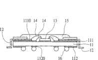
另请参阅图1,美国专利第5,854,512号又揭示一种结合有球栅数组基板与导脚的半导体封装件,得以提供更高密度的I/O的能力,其主要是提供一上、下表面形成有第一线路111及第二线路112的基板11,并于该基板11上表面上通过一非导电胶而将一导脚架的多导脚12粘置于该第一线路111上,且于该基板11第一表面上连接安置一芯片13,并使该芯片13通过焊线14而电性连接至该第一线路111的焊指(finger)1110及该导脚12,接着在该基板11上形成包覆该芯片13及焊线14的封装胶体15,及在该基板11第二线路112的焊球垫(solder ballpad)1120上植设焊球16及弯折该导脚12,以构成一具导脚的球栅数组式半导体封装件,从而通过该导脚的设置提供额外的I/O数目。相关的技术内容亦可参阅美国专利第4,763,188、5,420,758、5,365,409、5,438,478、5,386,141、5,283,717、5,502,289等。Please also refer to FIG. 1. US Patent No. 5,854,512 discloses a semiconductor package combined with a ball grid array substrate and pins to provide higher density I/O capabilities. It mainly provides an upper and lower surface The
但是这种方法较现有的球栅数组式(BGA)半导体封装件的工艺仍然成本太高而无法为业界所接受。However, this method is still too expensive to be accepted by the industry compared with the existing ball grid array (BGA) semiconductor packaging process.
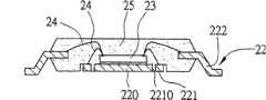
请参阅图2A至2E,鉴于此,美国专利第6,876,068号从而揭示一种不需使用昂贵的BGA基板结构而可增加电性输入/输出端(I/O)的导线架式半导体封装件及其制法,其提供一导线架22,该导线架22具有一芯片座220、多设于该芯片座220内部周围的第一导脚221、及多围绕设于该芯片座220外部且间隔一段距离的第二导脚222,其中该第一导脚221间形成有相间隔的开槽2210,并设有连接的第一连杆2211,该第二导脚进一步设有相连的第二连杆2221(如图2A及2B所示,其中该图2B为对应图2A的的剖面示意图);以供一芯片23连接安置于该芯片座220上,并通过多焊线24电性连接至该第一导脚221及第二导脚222(如图2C所示),再形成包覆该芯片23、芯片座220、第一导脚221及部分第二导脚222的封装胶体25,并使该芯片座220下表面、第一导脚221下表面及第二导脚222外端部分外露出该封装胶体25(如图2D所示),之后再对该第一连杆2211进行蚀刻或切割作业,以分离各所述第一导脚221,以及分离、弯折各所述第二导脚222,从而通过第一导脚221的设置而增加封装件可用的电性输入/输出端。2A to 2E, in view of this, U.S. Patent No. 6,876,068 discloses a lead frame semiconductor package that can increase electrical input/output terminals (I/O) without using an expensive BGA substrate structure and its Manufacturing method, it provides a
然而由于前述工艺中须利用蚀刻或切割方式分离各所述第一导脚,不仅工艺复杂且增加成本;再者在第一导脚经蚀刻或切割处因为封装胶体包覆不足,易发生裂损及湿气入侵的问题,另外该经蚀刻或切割处的第一导脚断面易发生氧化造成后续将封装件利用表面粘着技术(SMT)焊接于外部装置时,焊锡材料无法有效湿润(wetting)其上,造成焊接不良问题;此外,当第一导脚的排列密度高时,于封装模压时易造成该第一导脚的下表面因溢胶发生电性连接表面被封装胶体遮覆问题,而须额外进行去胶作业。However, in the aforementioned process, etching or cutting must be used to separate each of the first leads, which not only complicates the process but also increases the cost; moreover, cracks are prone to occur at the places where the first leads are etched or cut due to insufficient encapsulation. and the problem of moisture intrusion. In addition, the cross-section of the first lead pin at the etched or cut part is prone to oxidation, so that when the package is subsequently soldered to an external device using surface mount technology (SMT), the solder material cannot effectively wet it. In addition, when the arrangement density of the first pins is high, it is easy to cause the lower surface of the first pins to be covered by the encapsulation gel due to the overflow of glue when the package is molded. Additional de-glue work is required.
因此,如何提供一种低成本且具有多额外电性输入/输出端(I/O)的导架式半导体封装件及其制法,同时不需进行蚀刻、切割分离作业,以及可避免额外电性输入/输出端(I/O)发生裂损、湿气入侵、无法有效湿润、溢胶等问题,实为目前相关业界所亟待解决的课题。Therefore, how to provide a low-cost lead-frame semiconductor package with multiple additional electrical input/output terminals (I/O) and its manufacturing method, while eliminating the need for etching, cutting and separation operations, and avoiding additional electrical Problems such as cracks, moisture intrusion, ineffective wetting, and glue overflow of the permanent input/output (I/O) are issues that the relevant industries need to solve urgently.
发明内容Contents of the invention
鉴于以上现有的缺点,本发明的一个目的在于提供一种低成本且具有多额外电性输入/输出端(I/O)的半导体封装件及其制法。In view of the above existing shortcomings, an object of the present invention is to provide a low-cost semiconductor package with multiple additional electrical input/output terminals (I/O) and its manufacturing method.
本发明的又一目的是提供一种不需进行蚀刻、切割分离作业的半导体封装件及其制法。Another object of the present invention is to provide a semiconductor package and its manufacturing method that do not require etching, dicing and separation operations.
本发明的又一目的是提供一种可避免额外电性输入/输出端(I/O)发生裂损及湿气入侵的半导体封装件及其制法。Another object of the present invention is to provide a semiconductor package and its manufacturing method which can avoid crack damage and moisture intrusion of additional electrical input/output terminals (I/O).
本发明的再一目的是提供一种可避免额外电性输入/输出端(I/O)无法有效湿润的半导体封装件及其制法。Another object of the present invention is to provide a semiconductor package and its manufacturing method which can prevent the additional electrical input/output (I/O) from being effectively wetted.
本发明的另一目的是提供一种可避免额外电性输入/输出端(I/O)发生溢胶问题的半导体封装件及其制法。Another object of the present invention is to provide a semiconductor package and its manufacturing method which can avoid the glue overflow problem of the extra electrical input/output (I/O).
为达上述目的及其它相关的目的,本发明提供一种半导体封装件的制法,包括:提供导线架及表面布设有多连接垫的载板,该导线架具有芯片座及多围绕该芯片座周围的导脚,以将该该芯片座连接安置于该载板的上表面,其中该载板的平面尺寸大于芯片座平面尺寸,以使该载板上表面的连接垫外露出该芯片座;将至少一芯片连接安置于该芯片座与载板接合的一侧;通过多焊线以供该芯片电性连接至该载板上表面的连接垫及导线架的导脚;以及形成包覆该芯片、焊线及部分载板与导线架的封装胶体,并使该载板下表面及导脚部分外露出该封装胶体。该载板上表面进一步形成有连接安置垫以供导线架的芯片座连接安置于其上,且该载板上表面的连接安置垫及连接垫可通过形成于该载板中的导电结构而电性连接至载板下表面的连接垫。In order to achieve the above-mentioned purpose and other related purposes, the present invention provides a method for manufacturing a semiconductor package, comprising: providing a lead frame and a carrier plate with a plurality of connection pads on the surface, the lead frame has a chip holder and a plurality of chips surrounding the chip holder surrounding guide pins, so that the chip holder is connected and placed on the upper surface of the carrier board, wherein the planar size of the carrier board is larger than the planar size of the chip holder, so that the connection pad on the upper surface of the carrier board exposes the chip holder; At least one chip is connected to the side where the chip base is bonded to the carrier board; the chip is electrically connected to the connection pad on the upper surface of the carrier board and the lead pin of the lead frame through multiple bonding wires; Chips, bonding wires, part of the carrier board and the lead frame are encapsulated, and the lower surface of the carrier board and the guide pin part are exposed to the encapsulated gel. The upper surface of the carrier board is further formed with connection placement pads for the connection and placement of the chip base of the lead frame, and the connection placement pads and connection pads on the upper surface of the carrier board can be electrically connected through the conductive structure formed in the carrier board. connected to the connection pads on the lower surface of the carrier board.
该导线架导脚至载板下表面的距离略大于封装模具的模穴深度,以供进行封装模压作业时,使该载板顶抵于模穴,以避免发生溢胶间题。The distance from the guide pin of the lead frame to the lower surface of the carrier board is slightly larger than the cavity depth of the packaging mold, so that the carrier board can be pushed against the mold cavity during the packaging molding operation to avoid glue overflow.
本发明中还可使芯片通过接地焊线而电性连接至导线架的芯片座或载板的连接安置垫,以提升封装件电性品质;另外该导线架的芯片座平面尺寸可选择小于芯片的平面尺寸,以供芯片通过接地焊线电性连接至该载板的连接安置垫;进一步可在该载板上表面的连接垫上连接安置并电性连接被动组件,以提升封装件电性品质;再者,该导线架可采用四方扁平无导脚式导线架,以使该四方扁平无导脚式导线架的导脚下表面与该载板下表面约略同平面并外露出封装胶体。In the present invention, the chip can also be electrically connected to the chip seat of the lead frame or the connection placement pad of the carrier board through the grounding bonding wire, so as to improve the electrical quality of the package; in addition, the chip seat plane size of the lead frame can be selected to be smaller than the chip The plane size is for the chip to be electrically connected to the connection pad of the carrier board through the grounding wire; further, the connection pad on the upper surface of the carrier board can be connected and electrically connected to the passive component to improve the electrical quality of the package Furthermore, the lead frame can be a square flat non-lead lead frame, so that the lower surface of the guide pin of the square flat non-lead lead frame is approximately in the same plane as the lower surface of the carrier board and the encapsulation compound is exposed.
该芯片可直接连接安置于该芯片座上,或者该导线架的芯片座中进一步可形成有开口,以供芯片收纳于该开口中且连接安置于载板上;以及该载板表面还可覆盖一拒焊层,该拒焊层形成有外露出连接垫的开孔,并于外露出该开孔的连接垫上植设导电组件,从而通过该导电组件的设置以供封装件易于连接至外部装置。The chip can be directly connected and placed on the chip seat, or an opening can be further formed in the chip seat of the lead frame, so that the chip can be accommodated in the opening and connected and placed on the carrier plate; and the surface of the carrier plate can also cover A solder repelling layer, the solder repelling layer is formed with an opening that exposes the connection pad, and a conductive component is planted on the connection pad that exposes the opening, so that the package can be easily connected to an external device through the setting of the conductive component .
通过前述的制法,本发明进一步揭示一种半导体封装件,包括:导线架,具有一芯片座及多围绕于该芯片座周围的导脚,该芯片座具有相对的上表面及下表面;连接安置于该芯片座下表面的载板,该载板表面形成有多连接垫,且该载板的平面尺寸大于芯片座平面尺寸,以使该载板上表面的连接垫外露出该芯片座;至少一芯片,连接安置于该芯片座与载板接合的一侧,且通过焊线而电性连接至该载板的连接垫及导线架的导脚;以及封装胶体,包覆该芯片、焊线及部分载板与导线架,并使该载板下表面及导脚部分外露出该封装胶体。Through the foregoing manufacturing method, the present invention further discloses a semiconductor package, comprising: a lead frame having a chip seat and a plurality of guide pins surrounding the chip seat, the chip seat has opposite upper and lower surfaces; The carrier board placed on the lower surface of the chip holder, the surface of the carrier board is formed with multiple connection pads, and the planar size of the carrier board is larger than the planar size of the chip holder, so that the connection pads on the upper surface of the carrier board expose the chip holder; At least one chip is connected and placed on the side where the chip holder is bonded to the carrier board, and is electrically connected to the connection pad of the carrier board and the lead pin of the lead frame through welding wires; and the packaging compound covers the chip, solders wires and part of the carrier board and the lead frame, and expose the encapsulant on the lower surface of the carrier board and part of the guide pins.
因此本发明的半导体封装件及其制法,是预先制备一表面设有多连接垫的载板,以将该载板置于导线架的芯片座下表面,其中该载板平面尺寸大于芯片座平面尺寸,从而外露出该载板连接垫,并于该芯片座上表面连接安置至少一芯片,且使该芯片通过多焊线电性连接至该载板连接垫及导线架的导脚,再形成包覆该芯片、焊线及部分载板与导线架的封装胶体,并使该载板下表面及导脚部分外露出该封装胶体,如此即可通过该载板的连接垫增加芯片的电性输入/输出端(I/O),无须如同现有技术般通过在芯片座中增设多额外导脚,而在进行封装模压作业发生溢胶,及为去除溢胶所造成工艺繁杂问题,同时避免在进行这所述额外导脚分离所造成工艺步骤及成本增加问题,以及避免于该额外导脚分离后因封装胶体包覆不足而发生裂损、湿气入侵及因氧化而无法供焊锡材料有效湿润,进而造成焊接不良的问题。Therefore, the semiconductor package of the present invention and its manufacturing method are to pre-prepare a carrier board with multiple connection pads on the surface, so that the carrier board is placed on the lower surface of the chip holder of the lead frame, wherein the plane size of the carrier board is larger than that of the chip holder. planar size, thereby exposing the carrier board connection pad, and at least one chip is connected and placed on the upper surface of the chip holder, and the chip is electrically connected to the carrier board connection pad and the lead pin of the lead frame through multiple bonding wires, and then Form the encapsulant that covers the chip, bonding wires, part of the carrier and the lead frame, and expose the lower surface of the carrier and part of the lead pins, so that the chip's electrical resistance can be increased through the connection pad of the carrier. The input/output terminal (I/O) does not need to add more extra pins in the chip holder as in the prior art, and the glue overflow occurs during the packaging and molding operation, and the process of removing the overflow glue causes complicated problems, and at the same time Avoid the problems of process steps and cost increase caused by the separation of the additional leads, and avoid cracks, moisture intrusion, and inability to supply solder materials due to insufficient encapsulation after the separation of the additional leads. Effective wetting, which in turn causes poor soldering problems.
附图说明Description of drawings
图1为美国专利第5,854,512号所揭示的结合有球栅数组基板与导脚的半导体封装件示意图;FIG. 1 is a schematic diagram of a semiconductor package combined with a ball grid array substrate and leads disclosed in US Patent No. 5,854,512;
图2A至2E为美国专利第6,876,068号所揭示的可增加电性输入/输出端(I/O)的导线架式半导体封装件示意图;2A to 2E are schematic diagrams of lead frame semiconductor packages disclosed in US Pat. No. 6,876,068 that can add electrical input/output terminals (I/O);
图3A至3E为本发明的半导体封装件及其制法第一实施例的示意图;3A to 3E are schematic diagrams of a first embodiment of a semiconductor package and its manufacturing method of the present invention;
图4A至4C为本发明的半导体封装件及其制法第二实施例的示意图;4A to 4C are schematic diagrams of a second embodiment of the semiconductor package and its manufacturing method of the present invention;
图5为本发明的半导体封装件及其制法第三实施例的示意图;5 is a schematic diagram of a third embodiment of the semiconductor package and its manufacturing method of the present invention;
图6为本发明的半导体封装件及其制法第四实施例的示意图;6 is a schematic diagram of a fourth embodiment of the semiconductor package and its manufacturing method of the present invention;
图7为本发明的半导体封装件及其制法第五实施例的示意图;7 is a schematic diagram of a fifth embodiment of the semiconductor package and its manufacturing method of the present invention;
图8为本发明的半导体封装件及其制法第六实施例的示意图;以及8 is a schematic diagram of a sixth embodiment of the semiconductor package and its manufacturing method of the present invention; and
图9为本发明的半导体封装件及其制法第七实施例的示意图。FIG. 9 is a schematic diagram of a seventh embodiment of the semiconductor package and its manufacturing method of the present invention.
主要组件符号说明Explanation of main component symbols
11 载板11 carrier board
111 第一线路111 first line
1110 焊指1110 welding finger
112 第二线路112 Second Line
1120 焊球垫1120 Solder ball pad
12 导脚12 guide pins
13 芯片13 chips
14 焊线14 welding wire
15 封装胶体15 Encapsulation colloid
16 焊球16 solder balls
22 导线架22 lead frame
220 芯片座220 chip holder
221 第一导脚221 The first guide pin
2210 开槽2210 slotting
2211 第一连杆2211 The first connecting rod
222 第二导脚222 Second guide pin
2221 第二连杆2221 Second connecting rod
23 芯片23 chips
24 焊线24 welding wire
25 封装胶体25 Encapsulating colloid
31 载板31 carrier board
311 连接垫311 Connection pad
312 连接安置垫312 Connection placement pad
313 导电结构313 Conductive structure
32 导线架32 Lead frame
32’ 四方扁平无导脚式导线架32' Square flat lead-free lead frame
320,320’ 芯片座320, 320’ chip holder
322,322’ 导脚322, 322’ guide pin
3200 开口3200 opening
33 芯片33 chips
34 焊线34 welding wire
34’ 接地焊线34' ground wire
35 封装胶体35 Encapsulating colloid
36 拒焊层36 Solder repellent layer
37 导电组件37 Conductive components
38 被动组件38 Passive components
H 距离H distance
具体实施方式Detailed ways
以下是通过特定的具体实施例说明本发明的实施方式,所属技术领域中具有通常知识者可由本说明书所揭示内容轻易地了解本发明的其它优点与功效。The implementation of the present invention is described below through specific specific examples. Those skilled in the art can easily understand other advantages and effects of the present invention from the content disclosed in this specification.
第一实施例first embodiment
请参阅图3A至3E为本发明的半导体封装件及其制法的示意图。Please refer to FIGS. 3A to 3E , which are schematic diagrams of the semiconductor package and its manufacturing method of the present invention.
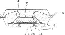
如图3A及3B所示,首先提供一导线架32及表面布设有多连接垫311的载板31,该导线架32具有芯片座320及多个围绕该芯片座周围的导脚322,以将该载板31粘附于该芯片座320的下表面,其中该载板31的平面尺寸大于芯片座320平面尺寸,以使该载板31上表面的连接垫311外露出该芯片座320。As shown in Figures 3A and 3B, a
该载板31上、下表面的连接垫311通过形成于该载板31中的导电结构313如通孔(via)而相互电性连接,另外在该载板31上表面进一步设有连接安置垫312,该导线架32、连接安置垫312与连接垫311主要材质为金属铜,并镀有如镍/金(Ni/Au)的金属层,以供焊线连接,其中该导线架32的芯片座320连接安置于该载板31上表面的连接安置垫312上,且该连接安置垫312可通过形成于载板31中的导电结构313连接至载板31另一表面的连接垫311,如此即可供芯片通过导线架31的芯片座31、连接安置垫312、导电结构313及连接垫311电性连通至外界。本发明中该载板31的制作远较传统球栅数组式(BGA)基板简单,不须经过繁复的线路设计与布局,故可有效节省成本。The
如图3C至3E所示,其中该3D图为对应图3C的上视图,将至少一芯片33连接安置于该芯片座320上表面,该芯片33可通过例如银胶(未图标)而粘置于该芯片座320上。As shown in Figures 3C to 3E, wherein the 3D figure is a top view corresponding to Figure 3C, at least one
接着利用多焊线34以供该芯片33电性连接至该载板31上表面的连接垫311及导线架32的导脚322,并通过封装模压作业以形成包覆该芯片33、焊线34及部分载板31与导线架32的封装胶体35,且使该载板31下表面及导脚322外端部分外露出该封装胶体35。Then use
如图3C所示,该导线架32的导脚322下表面距离该载板31下表面的距离H略大于封装模具(未图标)的深度约2-8密耳(mils),如此在进行封装模压作业时,即可使该载板31顶抵于封装模具的模穴,借以避免在填充封装树脂时发生溢胶问题。As shown in FIG. 3C , the distance H between the lower surface of the
如此即可通过该载板31的连接垫311提供芯片33额外的电性输入/输出端(I/O)。In this way, additional electrical input/output terminals (I/O) of the
通过前述制法,本发明进一步揭示一种半导体封装件,包括:导线架32,具有一芯片座320及多个围绕于该芯片座320周围的导脚322,该芯片座320具有相对的上表面及下表面;连接安置于该芯片座320下表面的载板31,该载板31表面形成有多连接垫311,且该载板31的平面尺寸大于芯片座320平面尺寸,以使该载板31上表面的连接垫311外露出该芯片座320;至少一芯片33,连接安置于该芯片座320上表面,且通过多焊线34电性连接至该载板31的连接垫311及导线架32的导脚322;以及封装胶体35,包覆该芯片33、焊线34及部分载板31与导线架32,并使该载板31下表面及导脚322外端部分外露出该封装胶体35。Through the foregoing manufacturing method, the present invention further discloses a semiconductor package, including: a
因此本发明的半导体封装件及其制法,是预先制备一表面设有多连接垫的载板,以将该载板置于导线架的芯片座下表面,其中该载板平面尺寸大于芯片座平面尺寸,以外露出该载板连接垫,并于该芯片座上表面连接安置至少一芯片,且使该芯片通过多焊线电性连接至该载板连接垫及导线架的导脚,再形成包覆该芯片、焊线及部分载板与导线架的封装胶体,并使该载板下表面及导脚部分外露出该封装胶体,如此即可通过该载板的连接垫增加芯片的电性输入/输出端(I/O),毋须如同现有技术般通过在芯片座中增设多额外导脚,而在进行封装模压作业发生溢胶及为去除溢胶所造成工艺繁杂问题,同时避免在进行这些额外导脚分离所造成工艺步骤及成本增加问题,以及避免在该额外导脚分离后因封装胶体包覆不足而发生裂损、湿气入侵及因氧化而无法供焊锡材料有效湿润,进而造成焊接不良的问题。Therefore, the semiconductor package of the present invention and its manufacturing method are to pre-prepare a carrier board with multiple connection pads on the surface, so that the carrier board is placed on the lower surface of the chip holder of the lead frame, wherein the plane size of the carrier board is larger than that of the chip holder. planar size, exposing the connecting pads of the carrier board, and connecting and placing at least one chip on the upper surface of the chip holder, and making the chip electrically connected to the connecting pads of the carrier board and the guide pins of the lead frame through multiple bonding wires, and then forming Coating the chip, bonding wires, part of the carrier board and the lead frame packaging compound, and exposing the packaging compound on the lower surface of the carrier board and the lead pins, so that the electrical properties of the chip can be increased through the connection pad of the carrier board The input/output (I/O) does not need to add more extra pins in the chip base as in the prior art, and the glue overflow during the packaging and molding operation and the complicated process caused by the removal of the overflow glue are avoided. The problems of process steps and cost increase caused by the separation of these additional leads, and the avoidance of cracks, moisture intrusion, and inability to effectively wet the solder material due to insufficient encapsulation gel coating after the separation of the additional leads, and then Causes poor welding problems.
第二实施例second embodiment
请参阅图4A至4C,为本发明的半导体封装件及其制法第二实施例的示意图,其中为便于说明及了解,对应先前相同或相似的组件是以相同编号表示的。Please refer to FIGS. 4A to 4C , which are schematic diagrams of the second embodiment of the semiconductor package and its manufacturing method of the present invention, wherein for the convenience of description and understanding, the same or similar components corresponding to the previous ones are denoted by the same numbers.
本实施例的半导体封装件与前述实施例大致相同,主要差异是提供芯片接地功能,进而提升封装件的电性品质。The semiconductor package of this embodiment is substantially the same as the previous embodiments, and the main difference is to provide a chip grounding function, thereby improving the electrical quality of the package.
如图4A所示,使芯片33通过接地焊线34’电性连接至该导线架32的芯片座320,再经由载板31的连接安置垫312、导电结构313连通至连接垫311。As shown in FIG. 4A , the
如图4B所示,使载板31的连接安置垫312平面尺寸大于导线架32的芯片座320平面尺寸,以供芯片33通过接地焊线34’电性连接至外露出该芯片座320的连接安置垫312上。As shown in FIG. 4B , the planar size of the
如图4C所示,使芯片33通过接地焊线34’电性连接至该导线架32的芯片座320,再自该芯片座320通过另一接地焊线34’电性连接至载板31的连接安置垫312,以供后续经由该导电结构313连通至连接垫311,进而再连接至如印刷电路板(未图标)等外部装置,以提升电性品质。As shown in FIG. 4C , the
第三实施例third embodiment
请参阅图5,为本发明的半导体封装件及其制法第三实施例的示意图,其中为便于说明及了解,对应先前相同或相似的组件是以相同编号表示的。Please refer to FIG. 5 , which is a schematic diagram of a third embodiment of the semiconductor package and its manufacturing method of the present invention, wherein for the convenience of description and understanding, the same or similar components corresponding to the previous ones are denoted by the same numbers.
本实施例的半导体封装件与前述实施例大致相同,主要差异在导线架32的芯片座320中形成有开口3200,以供芯片33收纳于该开口3200中且连接安置于载板31的连接安置垫312上。The semiconductor package of this embodiment is substantially the same as the previous embodiment, the main difference is that an
另外该芯片33可通过接地焊线34’电性连接至外露出该芯片座开孔3200中的连接安置垫312上,该连接安置垫312的材质例为金属铜且镀有如镍/金(Ni/Au)的金属层,以供焊线连接,再者该连接安置垫312可通过形成于载板31中的导电结构313连接至载板31另一表面的连接垫311。In addition, the
第四实施例Fourth embodiment
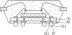
请参阅图6,为本发明的半导体封装件及其制法第四实施例的示意图,其中为便于说明及了解,对应先前相同或相似的组件是以相同编号表示的。Please refer to FIG. 6 , which is a schematic view of a fourth embodiment of the semiconductor package and its manufacturing method of the present invention, wherein for the convenience of description and understanding, the same or similar components are denoted by the same numbers.
本实施例的半导体封装件及其制法与前述实施例大致相同,主要差异在于该载板31表面进一步可覆盖一拒焊层36,该拒焊层36形成有开孔以外露出连接垫311,并于外露出该开孔的连接垫311上植设导电组件37,以提供多高密度的电性输入/输出端(I/O),同时通过该导电组件37的设置更可使封装件易于连接至如印刷电路板(PCB)的外部装置上。The semiconductor package and its manufacturing method of this embodiment are substantially the same as those of the foregoing embodiments, the main difference being that the surface of the
第五实施例fifth embodiment
请参阅图7,为本发明的半导体封装件及其制法第五实施例的示意图,其中为便于说明及了解,对应先前相同或相似的组件是以相同编号表示的。Please refer to FIG. 7 , which is a schematic diagram of a fifth embodiment of the semiconductor package and its manufacturing method of the present invention, wherein for the convenience of description and understanding, the same or similar components are denoted by the same numbers.
本实施例的半导体封装件及其制法与前述实施例大致相同,主要差异在于导线架32的芯片座320平面尺寸可选择小于芯片33平面尺寸,以缩小芯片33与芯片座320接触面积,避免芯片33与该芯片座320间因热膨胀系数不同,受热应力作用而容易发生剥离问题,且可供该芯片33通过接地焊线34’电性连接至载板31的连接安置垫312,以提升封装件电性品质。The semiconductor package of the present embodiment and its manufacturing method are substantially the same as those of the foregoing embodiments, the main difference being that the planar size of the
第六实施例Sixth embodiment
请参阅图8,为本发明的半导体封装件及其制法第六实施例的示意图,其中为便于说明及了解,对应先前相同或相似的组件是以相同编号表示的。Please refer to FIG. 8 , which is a schematic diagram of a sixth embodiment of the semiconductor package and its manufacturing method of the present invention, wherein for the convenience of description and understanding, the same or similar components are denoted by the same numbers.
本实施例的半导体封装件及其制法与前述实施例大致相同,主要差异是可在载板31上表面的连接垫311上连接安置并电性连接有被动组件38,借以提升封装件的电性功能及品质。The semiconductor package and its manufacturing method of this embodiment are substantially the same as those of the previous embodiments, the main difference being that the
第七实施例Seventh embodiment
请参阅图9,为本发明的半导体封装件及其制法第七实施例的示意图,其中为便于说明及了解,对应先前相同或相似的组件是以相同编号表示的。Please refer to FIG. 9 , which is a schematic diagram of a seventh embodiment of the semiconductor package and its manufacturing method of the present invention, wherein for the convenience of description and understanding, the same or similar components corresponding to the previous ones are denoted by the same numbers.
本实施例的半导体封装件及其制法与前述实施例大致相同,主要差异是使用四方扁平无导脚(Quad Flat Non-leaded,QFN)式导线架32’,并使其芯片座320’连接安置于该载板31上,且令该载板31下表面与该四方扁平无导脚式导线架32’的导脚322’下表面约略共平面,再进行置晶、打线及封装模压作业,以使封装胶体35包覆该芯片33、焊线34、导线架32’及载板31,并令该载板31下表面及该四方扁平无导脚导线架32’的导脚322’下表面外露出该封装胶体35。The semiconductor package and its manufacturing method of this embodiment are roughly the same as those of the previous embodiments, the main difference is that a Quad Flat Non-leaded (QFN) lead frame 32' is used, and the chip base 320' is connected to Place on the
上述的具体实施例,仅用以例释本发明的特点及功效,而非用以限定本发明。任何所属技术领域中具有通常知识者均可在不违背本发明的精神及范畴下,对于上述的实施例进行修饰与改变。因此,本发明的权利保护范围,应如申请专利权利要求范围所列。The above specific embodiments are only used to illustrate the features and functions of the present invention, rather than to limit the present invention. Anyone skilled in the art can make modifications and changes to the above-mentioned embodiments without departing from the spirit and scope of the present invention. Therefore, the protection scope of the present invention should be as listed in the scope of the patent application claims.
Claims (38)
Translated fromChinesePriority Applications (1)
| Application Number | Priority Date | Filing Date | Title |
|---|---|---|---|
| CN2007101477234ACN101378023B (en) | 2007-08-27 | 2007-08-27 | Semiconductor package and fabrication method thereof |
Applications Claiming Priority (1)
| Application Number | Priority Date | Filing Date | Title |
|---|---|---|---|
| CN2007101477234ACN101378023B (en) | 2007-08-27 | 2007-08-27 | Semiconductor package and fabrication method thereof |
Publications (2)
| Publication Number | Publication Date |
|---|---|
| CN101378023A CN101378023A (en) | 2009-03-04 |
| CN101378023Btrue CN101378023B (en) | 2010-12-01 |
Family
ID=40421490
Family Applications (1)
| Application Number | Title | Priority Date | Filing Date |
|---|---|---|---|
| CN2007101477234AExpired - Fee RelatedCN101378023B (en) | 2007-08-27 | 2007-08-27 | Semiconductor package and fabrication method thereof |
Country Status (1)
| Country | Link |
|---|---|
| CN (1) | CN101378023B (en) |
Families Citing this family (2)
| Publication number | Priority date | Publication date | Assignee | Title |
|---|---|---|---|---|
| CN103824756B (en)* | 2012-11-16 | 2017-12-05 | 中芯国际集成电路制造(上海)有限公司 | The method for removing encapsulating structure |
| CN110890023A (en)* | 2019-11-20 | 2020-03-17 | 厦门天马微电子有限公司 | Display module, manufacturing method thereof and display device |
Citations (2)
| Publication number | Priority date | Publication date | Assignee | Title |
|---|---|---|---|---|
| CN1354508A (en)* | 2000-11-17 | 2002-06-19 | 矽品精密工业股份有限公司 | Semiconductor package with exposed die paddle |
| CN1466206A (en)* | 2002-06-28 | 2004-01-07 | ��Ʒ���ܹ�ҵ�ɷ�����˾ | Ball Grid Array Semiconductor Package |
- 2007
- 2007-08-27CNCN2007101477234Apatent/CN101378023B/ennot_activeExpired - Fee Related
Patent Citations (2)
| Publication number | Priority date | Publication date | Assignee | Title |
|---|---|---|---|---|
| CN1354508A (en)* | 2000-11-17 | 2002-06-19 | 矽品精密工业股份有限公司 | Semiconductor package with exposed die paddle |
| CN1466206A (en)* | 2002-06-28 | 2004-01-07 | ��Ʒ���ܹ�ҵ�ɷ�����˾ | Ball Grid Array Semiconductor Package |
Non-Patent Citations (2)
| Title |
|---|
| CN 1466206 A,说明书第1页第5行-第8页第23行、附图1-6. |
| JP特开平6-333979A 1994.12.02 |
Also Published As
| Publication number | Publication date |
|---|---|
| CN101378023A (en) | 2009-03-04 |
Similar Documents
| Publication | Publication Date | Title |
|---|---|---|
| US9130064B2 (en) | Method for fabricating leadframe-based semiconductor package with connecting pads top and bottom surfaces of carrier | |
| US6781242B1 (en) | Thin ball grid array package | |
| CN102201385B (en) | Quad flat no-lead semiconductor package and manufacturing method thereof | |
| US7816187B2 (en) | Method for fabricating semiconductor package free of substrate | |
| US8455304B2 (en) | Routable array metal integrated circuit package fabricated using partial etching process | |
| CN110010489B (en) | Method for fabricating semiconductor device with sidewall recesses and related device | |
| US8981575B2 (en) | Semiconductor package structure | |
| US7939383B2 (en) | Method for fabricating semiconductor package free of substrate | |
| KR101119708B1 (en) | Land grid array packaged device and method of forming same | |
| CN101350318B (en) | Electronic package and electronic device | |
| US7423340B2 (en) | Semiconductor package free of substrate and fabrication method thereof | |
| US20090206459A1 (en) | Quad flat non-leaded package structure | |
| US20100295160A1 (en) | Quad flat package structure having exposed heat sink, electronic assembly and manufacturing methods thereof | |
| CN111834323A (en) | A semiconductor package and its manufacturing method | |
| CN101378023B (en) | Semiconductor package and fabrication method thereof | |
| CN216624270U (en) | Semiconductor packages and electronic devices | |
| JPH11297917A (en) | Semiconductor device and its manufacture | |
| CN201229938Y (en) | Chip packaging structure | |
| US20050194665A1 (en) | Semiconductor package free of substrate and fabrication method thereof | |
| KR100437821B1 (en) | semiconductor package and metod for fabricating the same | |
| KR100351920B1 (en) | semiconductor device and method for fabricating the same | |
| US20050184368A1 (en) | Semiconductor package free of substrate and fabrication method thereof | |
| KR20010009374A (en) | Method for manufacturing package | |
| KR20020049821A (en) | chip scale semiconductor package in wafer level and method for fabricating the same | |
| KR20120043867A (en) | Semiconductor package and method of manufacturing the same |
Legal Events
| Date | Code | Title | Description |
|---|---|---|---|
| C06 | Publication | ||
| PB01 | Publication | ||
| C10 | Entry into substantive examination | ||
| SE01 | Entry into force of request for substantive examination | ||
| C14 | Grant of patent or utility model | ||
| GR01 | Patent grant | ||
| CF01 | Termination of patent right due to non-payment of annual fee | ||
| CF01 | Termination of patent right due to non-payment of annual fee | Granted publication date:20101201 Termination date:20210827 |