CN101369634A - Light emitting device and manufacturing method thereof - Google Patents
Light emitting device and manufacturing method thereofDownload PDFInfo
- Publication number
- CN101369634A CN101369634ACNA2008101687237ACN200810168723ACN101369634ACN 101369634 ACN101369634 ACN 101369634ACN A2008101687237 ACNA2008101687237 ACN A2008101687237ACN 200810168723 ACN200810168723 ACN 200810168723ACN 101369634 ACN101369634 ACN 101369634A
- Authority
- CN
- China
- Prior art keywords
- light
- film
- light emitting
- emitting device
- layer
- Prior art date
- Legal status (The legal status is an assumption and is not a legal conclusion. Google has not performed a legal analysis and makes no representation as to the accuracy of the status listed.)
- Granted
Links
- 238000004519manufacturing processMethods0.000titleclaimsabstractdescription45
- 239000010408filmSubstances0.000claimsabstractdescription364
- 229910052739hydrogenInorganic materials0.000claimsabstractdescription141
- 239000001257hydrogenSubstances0.000claimsabstractdescription138
- UFHFLCQGNIYNRP-UHFFFAOYSA-NHydrogenChemical compound[H][H]UFHFLCQGNIYNRP-UHFFFAOYSA-N0.000claimsabstractdescription122
- 239000010409thin filmSubstances0.000claimsabstractdescription93
- 229910052581Si3N4Inorganic materials0.000claimsabstractdescription48
- HQVNEWCFYHHQES-UHFFFAOYSA-Nsilicon nitrideChemical compoundN12[Si]34N5[Si]62N3[Si]51N64HQVNEWCFYHHQES-UHFFFAOYSA-N0.000claimsabstractdescription48
- 230000001681protective effectEffects0.000claimsabstractdescription45
- 239000000758substrateSubstances0.000claimsdescription108
- 150000002894organic compoundsChemical class0.000claimsdescription90
- 238000000034methodMethods0.000claimsdescription56
- 238000007789sealingMethods0.000claimsdescription43
- 239000000463materialSubstances0.000claimsdescription38
- 230000007547defectEffects0.000claimsdescription28
- 230000015572biosynthetic processEffects0.000claimsdescription25
- 238000004544sputter depositionMethods0.000claimsdescription25
- 150000002431hydrogenChemical class0.000claimsdescription22
- 238000005268plasma chemical vapour depositionMethods0.000claimsdescription22
- 239000011159matrix materialSubstances0.000claimsdescription19
- 239000000956alloySubstances0.000claimsdescription16
- OKTJSMMVPCPJKN-UHFFFAOYSA-NCarbonChemical compound[C]OKTJSMMVPCPJKN-UHFFFAOYSA-N0.000claimsdescription15
- 229910052799carbonInorganic materials0.000claimsdescription15
- 238000001704evaporationMethods0.000claimsdescription15
- 229910045601alloyInorganic materials0.000claimsdescription14
- 229910052782aluminiumInorganic materials0.000claimsdescription10
- 239000004020conductorSubstances0.000claimsdescription10
- 239000010936titaniumSubstances0.000claimsdescription9
- 229910052750molybdenumInorganic materials0.000claimsdescription8
- 238000000576coating methodMethods0.000claimsdescription7
- 229910052719titaniumInorganic materials0.000claimsdescription7
- 230000001413cellular effectEffects0.000claimsdescription6
- XAGFODPZIPBFFR-UHFFFAOYSA-NaluminiumChemical compound[Al]XAGFODPZIPBFFR-UHFFFAOYSA-N0.000claimsdescription5
- 239000010949copperSubstances0.000claimsdescription5
- 229910052802copperInorganic materials0.000claimsdescription5
- RTAQQCXQSZGOHL-UHFFFAOYSA-NTitaniumChemical compound[Ti]RTAQQCXQSZGOHL-UHFFFAOYSA-N0.000claimsdescription3
- 238000007733ion platingMethods0.000claimsdescription3
- 239000011248coating agentSubstances0.000claimsdescription2
- RYGMFSIKBFXOCR-UHFFFAOYSA-NCopperChemical compound[Cu]RYGMFSIKBFXOCR-UHFFFAOYSA-N0.000claims2
- ZOKXTWBITQBERF-UHFFFAOYSA-NMolybdenumChemical compound[Mo]ZOKXTWBITQBERF-UHFFFAOYSA-N0.000claims2
- 239000011358absorbing materialSubstances0.000claims2
- 239000011733molybdenumSubstances0.000claims2
- 239000006117anti-reflective coatingSubstances0.000claims1
- 239000012212insulatorSubstances0.000abstractdescription32
- 229910052751metalInorganic materials0.000abstractdescription20
- 239000002184metalSubstances0.000abstractdescription20
- 238000003475laminationMethods0.000abstractdescription3
- 239000010410layerSubstances0.000description217
- 239000012535impuritySubstances0.000description50
- XUIMIQQOPSSXEZ-UHFFFAOYSA-NSiliconChemical compound[Si]XUIMIQQOPSSXEZ-UHFFFAOYSA-N0.000description34
- 229910052710siliconInorganic materials0.000description34
- 239000010703siliconSubstances0.000description34
- 239000007789gasSubstances0.000description33
- 239000004065semiconductorSubstances0.000description31
- 238000005530etchingMethods0.000description30
- 238000012546transferMethods0.000description24
- 238000010438heat treatmentMethods0.000description19
- IJGRMHOSHXDMSA-UHFFFAOYSA-NAtomic nitrogenChemical compoundN#NIJGRMHOSHXDMSA-UHFFFAOYSA-N0.000description16
- PXHVJJICTQNCMI-UHFFFAOYSA-NNickelChemical compound[Ni]PXHVJJICTQNCMI-UHFFFAOYSA-N0.000description16
- XLOMVQKBTHCTTD-UHFFFAOYSA-NZinc monoxideChemical compound[Zn]=OXLOMVQKBTHCTTD-UHFFFAOYSA-N0.000description16
- 239000011229interlayerSubstances0.000description14
- XKRFYHLGVUSROY-UHFFFAOYSA-NArgonChemical compound[Ar]XKRFYHLGVUSROY-UHFFFAOYSA-N0.000description12
- 229910052760oxygenInorganic materials0.000description12
- 229910052757nitrogenInorganic materials0.000description11
- 230000008569processEffects0.000description11
- MHAJPDPJQMAIIY-UHFFFAOYSA-NHydrogen peroxideChemical compoundOOMHAJPDPJQMAIIY-UHFFFAOYSA-N0.000description10
- 230000004888barrier functionEffects0.000description10
- 229910052718tinInorganic materials0.000description10
- 229910021417amorphous siliconInorganic materials0.000description9
- 239000012298atmosphereSubstances0.000description9
- 125000004429atomChemical group0.000description9
- QVGXLLKOCUKJST-UHFFFAOYSA-Natomic oxygenChemical compound[O]QVGXLLKOCUKJST-UHFFFAOYSA-N0.000description9
- 239000013078crystalSubstances0.000description9
- 238000002347injectionMethods0.000description9
- 239000007924injectionSubstances0.000description9
- 239000000203mixtureSubstances0.000description9
- 239000001301oxygenSubstances0.000description9
- KRHYYFGTRYWZRS-UHFFFAOYSA-NFluoraneChemical compoundFKRHYYFGTRYWZRS-UHFFFAOYSA-N0.000description8
- -1WSixInorganic materials0.000description8
- 150000002500ionsChemical class0.000description8
- 238000000059patterningMethods0.000description8
- 229910052721tungstenInorganic materials0.000description8
- 239000011787zinc oxideSubstances0.000description8
- 238000000137annealingMethods0.000description7
- 239000011651chromiumSubstances0.000description7
- 230000006870functionEffects0.000description7
- 239000011261inert gasSubstances0.000description7
- 229910052759nickelInorganic materials0.000description7
- OAICVXFJPJFONN-UHFFFAOYSA-NPhosphorusChemical compound[P]OAICVXFJPJFONN-UHFFFAOYSA-N0.000description6
- 229910052786argonInorganic materials0.000description6
- 238000005229chemical vapour depositionMethods0.000description6
- 229910052738indiumInorganic materials0.000description6
- 229910052698phosphorusInorganic materials0.000description6
- 239000011574phosphorusSubstances0.000description6
- BASFCYQUMIYNBI-UHFFFAOYSA-NplatinumChemical compound[Pt]BASFCYQUMIYNBI-UHFFFAOYSA-N0.000description6
- 229910021420polycrystalline siliconInorganic materials0.000description6
- 239000010937tungstenSubstances0.000description6
- 229910017073AlLiInorganic materials0.000description5
- 229910052804chromiumInorganic materials0.000description5
- 150000001875compoundsChemical class0.000description5
- 238000002425crystallisationMethods0.000description5
- 230000008025crystallizationEffects0.000description5
- 230000008020evaporationEffects0.000description5
- 238000005247getteringMethods0.000description5
- 230000001678irradiating effectEffects0.000description5
- AHLBNYSZXLDEJQ-FWEHEUNISA-NorlistatChemical compoundCCCCCCCCCCC[C@H](OC(=O)[C@H](CC(C)C)NC=O)C[C@@H]1OC(=O)[C@H]1CCCCCCAHLBNYSZXLDEJQ-FWEHEUNISA-N0.000description5
- 230000002093peripheral effectEffects0.000description5
- 229920005591polysiliconPolymers0.000description5
- VYPSYNLAJGMNEJ-UHFFFAOYSA-Nsilicon dioxideInorganic materialsO=[Si]=OVYPSYNLAJGMNEJ-UHFFFAOYSA-N0.000description5
- 238000004528spin coatingMethods0.000description5
- WFKWXMTUELFFGS-UHFFFAOYSA-NtungstenChemical compound[W]WFKWXMTUELFFGS-UHFFFAOYSA-N0.000description5
- 229910017911MgInInorganic materials0.000description4
- 229920001609Poly(3,4-ethylenedioxythiophene)Polymers0.000description4
- ATJFFYVFTNAWJD-UHFFFAOYSA-NTinChemical compound[Sn]ATJFFYVFTNAWJD-UHFFFAOYSA-N0.000description4
- 230000004913activationEffects0.000description4
- 239000003086colorantSubstances0.000description4
- 230000005281excited stateEffects0.000description4
- 230000005525hole transportEffects0.000description4
- PJXISJQVUVHSOJ-UHFFFAOYSA-Nindium(iii) oxideChemical compound[O-2].[O-2].[O-2].[In+3].[In+3]PJXISJQVUVHSOJ-UHFFFAOYSA-N0.000description4
- 239000011810insulating materialSubstances0.000description4
- 238000011068loading methodMethods0.000description4
- 239000002245particleSubstances0.000description4
- 230000000737periodic effectEffects0.000description4
- 229920001467poly(styrenesulfonates)Polymers0.000description4
- 238000007781pre-processingMethods0.000description4
- 238000012545processingMethods0.000description4
- 239000011347resinSubstances0.000description4
- 229920005989resinPolymers0.000description4
- 239000002356single layerSubstances0.000description4
- 229910052725zincInorganic materials0.000description4
- 239000011701zincSubstances0.000description4
- 239000004215Carbon black (E152)Substances0.000description3
- VYZAMTAEIAYCRO-UHFFFAOYSA-NChromiumChemical compound[Cr]VYZAMTAEIAYCRO-UHFFFAOYSA-N0.000description3
- MWUXSHHQAYIFBG-UHFFFAOYSA-NNitric oxideChemical compoundO=[N]MWUXSHHQAYIFBG-UHFFFAOYSA-N0.000description3
- 239000007864aqueous solutionSubstances0.000description3
- 230000015556catabolic processEffects0.000description3
- 238000007872degassingMethods0.000description3
- 238000006731degradation reactionMethods0.000description3
- 238000007865dilutingMethods0.000description3
- 239000011521glassSubstances0.000description3
- 229930195733hydrocarbonNatural products0.000description3
- 150000002430hydrocarbonsChemical class0.000description3
- 238000009616inductively coupled plasmaMethods0.000description3
- 238000005468ion implantationMethods0.000description3
- 230000003287optical effectEffects0.000description3
- 230000001590oxidative effectEffects0.000description3
- 229920000642polymerPolymers0.000description3
- 229910052814silicon oxideInorganic materials0.000description3
- 229910052715tantalumInorganic materials0.000description3
- ZOXJGFHDIHLPTG-UHFFFAOYSA-NBoronChemical compound[B]ZOXJGFHDIHLPTG-UHFFFAOYSA-N0.000description2
- 229910000846In alloyInorganic materials0.000description2
- XYFCBTPGUUZFHI-UHFFFAOYSA-NPhosphineChemical compoundPXYFCBTPGUUZFHI-UHFFFAOYSA-N0.000description2
- 229910000676Si alloyInorganic materials0.000description2
- NRTOMJZYCJJWKI-UHFFFAOYSA-NTitanium nitrideChemical compound[Ti]#NNRTOMJZYCJJWKI-UHFFFAOYSA-N0.000description2
- CSDREXVUYHZDNP-UHFFFAOYSA-NalumanylidynesiliconChemical compound[Al].[Si]CSDREXVUYHZDNP-UHFFFAOYSA-N0.000description2
- 229910052785arsenicInorganic materials0.000description2
- RQNWIZPPADIBDY-UHFFFAOYSA-Narsenic atomChemical compound[As]RQNWIZPPADIBDY-UHFFFAOYSA-N0.000description2
- 229910052796boronInorganic materials0.000description2
- 239000010406cathode materialSubstances0.000description2
- 230000008859changeEffects0.000description2
- 238000010549co-EvaporationMethods0.000description2
- 238000006356dehydrogenation reactionMethods0.000description2
- 238000011161developmentMethods0.000description2
- 230000018109developmental processEffects0.000description2
- 238000010586diagramMethods0.000description2
- 230000005283ground stateEffects0.000description2
- 238000005984hydrogenation reactionMethods0.000description2
- 229910003437indium oxideInorganic materials0.000description2
- 229910010272inorganic materialInorganic materials0.000description2
- 239000011147inorganic materialSubstances0.000description2
- 229910052749magnesiumInorganic materials0.000description2
- 230000007246mechanismEffects0.000description2
- 230000003647oxidationEffects0.000description2
- 238000007254oxidation reactionMethods0.000description2
- 239000000049pigmentSubstances0.000description2
- 238000002294plasma sputter depositionMethods0.000description2
- 229910052697platinumInorganic materials0.000description2
- 239000010453quartzSubstances0.000description2
- 238000004151rapid thermal annealingMethods0.000description2
- 239000012495reaction gasSubstances0.000description2
- 229910052709silverInorganic materials0.000description2
- 239000007921spraySubstances0.000description2
- 239000000126substanceSubstances0.000description2
- XOLBLPGZBRYERU-UHFFFAOYSA-Ntin dioxideChemical compoundO=[Sn]=OXOLBLPGZBRYERU-UHFFFAOYSA-N0.000description2
- 229910001887tin oxideInorganic materials0.000description2
- 238000002834transmittanceMethods0.000description2
- 239000004925Acrylic resinSubstances0.000description1
- 229920000178Acrylic resinPolymers0.000description1
- 241001269524DuraSpecies0.000description1
- KRHYYFGTRYWZRS-UHFFFAOYSA-MFluoride anionChemical compound[F-]KRHYYFGTRYWZRS-UHFFFAOYSA-M0.000description1
- 229910002668Pd-CuInorganic materials0.000description1
- BLRPTPMANUNPDV-UHFFFAOYSA-NSilaneChemical compound[SiH4]BLRPTPMANUNPDV-UHFFFAOYSA-N0.000description1
- 229910000577Silicon-germaniumInorganic materials0.000description1
- 101100489584Solanum lycopersicum TFT1 geneProteins0.000description1
- 101100214488Solanum lycopersicum TFT2 geneProteins0.000description1
- 101100214491Solanum lycopersicum TFT3 geneProteins0.000description1
- 229910001069Ti alloyInorganic materials0.000description1
- LEVVHYCKPQWKOP-UHFFFAOYSA-N[Si].[Ge]Chemical compound[Si].[Ge]LEVVHYCKPQWKOP-UHFFFAOYSA-N0.000description1
- MQRWBMAEBQOWAF-UHFFFAOYSA-Nacetic acid;nickelChemical compound[Ni].CC(O)=O.CC(O)=OMQRWBMAEBQOWAF-UHFFFAOYSA-N0.000description1
- 239000000853adhesiveSubstances0.000description1
- 230000001070adhesive effectEffects0.000description1
- UQZIWOQVLUASCR-UHFFFAOYSA-Nalumane;titaniumChemical compound[AlH3].[Ti]UQZIWOQVLUASCR-UHFFFAOYSA-N0.000description1
- 239000005407aluminoborosilicate glassSubstances0.000description1
- 239000012300argon atmosphereSubstances0.000description1
- 229910052788bariumInorganic materials0.000description1
- DSAJWYNOEDNPEQ-UHFFFAOYSA-Nbarium atomChemical compound[Ba]DSAJWYNOEDNPEQ-UHFFFAOYSA-N0.000description1
- 230000008901benefitEffects0.000description1
- 230000005540biological transmissionEffects0.000description1
- 239000005388borosilicate glassSubstances0.000description1
- 238000009125cardiac resynchronization therapyMethods0.000description1
- 239000000969carrierSubstances0.000description1
- 238000006243chemical reactionMethods0.000description1
- 238000004140cleaningMethods0.000description1
- 230000000295complement effectEffects0.000description1
- 238000000151depositionMethods0.000description1
- ZOCHARZZJNPSEU-UHFFFAOYSA-NdiboronChemical compoundB#BZOCHARZZJNPSEU-UHFFFAOYSA-N0.000description1
- PZPGRFITIJYNEJ-UHFFFAOYSA-NdisilaneChemical compound[SiH3][SiH3]PZPGRFITIJYNEJ-UHFFFAOYSA-N0.000description1
- 238000009826distributionMethods0.000description1
- 230000005684electric fieldEffects0.000description1
- 238000005401electroluminescenceMethods0.000description1
- 238000005516engineering processMethods0.000description1
- 238000000605extractionMethods0.000description1
- 230000005669field effectEffects0.000description1
- 230000006872improvementEffects0.000description1
- 230000005596ionic collisionsEffects0.000description1
- 239000004973liquid crystal related substanceSubstances0.000description1
- 238000004518low pressure chemical vapour depositionMethods0.000description1
- 238000005259measurementMethods0.000description1
- 239000012528membraneSubstances0.000description1
- 150000002739metalsChemical class0.000description1
- 229940078494nickel acetateDrugs0.000description1
- 150000004767nitridesChemical class0.000description1
- 239000012299nitrogen atmosphereSubstances0.000description1
- QJGQUHMNIGDVPM-UHFFFAOYSA-Nnitrogen groupChemical group[N]QJGQUHMNIGDVPM-UHFFFAOYSA-N0.000description1
- 239000012788optical filmSubstances0.000description1
- 239000011368organic materialSubstances0.000description1
- 230000035699permeabilityEffects0.000description1
- 238000009832plasma treatmentMethods0.000description1
- 229920003023plasticPolymers0.000description1
- 239000004033plasticSubstances0.000description1
- 230000010287polarizationEffects0.000description1
- 238000007639printingMethods0.000description1
- 238000001552radio frequency sputter depositionMethods0.000description1
- 230000009467reductionEffects0.000description1
- 238000011160researchMethods0.000description1
- 238000012827research and developmentMethods0.000description1
- 238000000926separation methodMethods0.000description1
- 229910000077silaneInorganic materials0.000description1
- 229910021332silicideInorganic materials0.000description1
- FVBUAEGBCNSCDD-UHFFFAOYSA-Nsilicide(4-)Chemical compound[Si-4]FVBUAEGBCNSCDD-UHFFFAOYSA-N0.000description1
- HBMJWWWQQXIZIP-UHFFFAOYSA-Nsilicon carbideChemical compound[Si+]#[C-]HBMJWWWQQXIZIP-UHFFFAOYSA-N0.000description1
- 229910010271silicon carbideInorganic materials0.000description1
- 239000000243solutionSubstances0.000description1
- 238000005507sprayingMethods0.000description1
- 239000010935stainless steelSubstances0.000description1
- 229910001220stainless steelInorganic materials0.000description1
- MZLGASXMSKOWSE-UHFFFAOYSA-Ntantalum nitrideChemical compound[Ta]#NMZLGASXMSKOWSE-UHFFFAOYSA-N0.000description1
- VEDJZFSRVVQBIL-UHFFFAOYSA-NtrisilaneChemical compound[SiH3][SiH2][SiH3]VEDJZFSRVVQBIL-UHFFFAOYSA-N0.000description1
Images


Classifications
- H—ELECTRICITY
- H05—ELECTRIC TECHNIQUES NOT OTHERWISE PROVIDED FOR
- H05B—ELECTRIC HEATING; ELECTRIC LIGHT SOURCES NOT OTHERWISE PROVIDED FOR; CIRCUIT ARRANGEMENTS FOR ELECTRIC LIGHT SOURCES, IN GENERAL
- H05B33/00—Electroluminescent light sources
- H—ELECTRICITY
- H10—SEMICONDUCTOR DEVICES; ELECTRIC SOLID-STATE DEVICES NOT OTHERWISE PROVIDED FOR
- H10K—ORGANIC ELECTRIC SOLID-STATE DEVICES
- H10K59/00—Integrated devices, or assemblies of multiple devices, comprising at least one organic light-emitting element covered by group H10K50/00
- H10K59/30—Devices specially adapted for multicolour light emission
- H10K59/38—Devices specially adapted for multicolour light emission comprising colour filters or colour changing media [CCM]
- H—ELECTRICITY
- H10—SEMICONDUCTOR DEVICES; ELECTRIC SOLID-STATE DEVICES NOT OTHERWISE PROVIDED FOR
- H10K—ORGANIC ELECTRIC SOLID-STATE DEVICES
- H10K50/00—Organic light-emitting devices
- H10K50/80—Constructional details
- H10K50/805—Electrodes
- H10K50/81—Anodes
- H10K50/814—Anodes combined with auxiliary electrodes, e.g. ITO layer combined with metal lines
- H—ELECTRICITY
- H10—SEMICONDUCTOR DEVICES; ELECTRIC SOLID-STATE DEVICES NOT OTHERWISE PROVIDED FOR
- H10K—ORGANIC ELECTRIC SOLID-STATE DEVICES
- H10K50/00—Organic light-emitting devices
- H10K50/80—Constructional details
- H10K50/805—Electrodes
- H10K50/82—Cathodes
- H10K50/824—Cathodes combined with auxiliary electrodes
- H—ELECTRICITY
- H10—SEMICONDUCTOR DEVICES; ELECTRIC SOLID-STATE DEVICES NOT OTHERWISE PROVIDED FOR
- H10K—ORGANIC ELECTRIC SOLID-STATE DEVICES
- H10K50/00—Organic light-emitting devices
- H10K50/80—Constructional details
- H10K50/84—Passivation; Containers; Encapsulations
- H10K50/844—Encapsulations
- H—ELECTRICITY
- H10—SEMICONDUCTOR DEVICES; ELECTRIC SOLID-STATE DEVICES NOT OTHERWISE PROVIDED FOR
- H10K—ORGANIC ELECTRIC SOLID-STATE DEVICES
- H10K59/00—Integrated devices, or assemblies of multiple devices, comprising at least one organic light-emitting element covered by group H10K50/00
- H10K59/10—OLED displays
- H10K59/12—Active-matrix OLED [AMOLED] displays
- H10K59/122—Pixel-defining structures or layers, e.g. banks
- H—ELECTRICITY
- H10—SEMICONDUCTOR DEVICES; ELECTRIC SOLID-STATE DEVICES NOT OTHERWISE PROVIDED FOR
- H10K—ORGANIC ELECTRIC SOLID-STATE DEVICES
- H10K59/00—Integrated devices, or assemblies of multiple devices, comprising at least one organic light-emitting element covered by group H10K50/00
- H10K59/10—OLED displays
- H10K59/12—Active-matrix OLED [AMOLED] displays
- H10K59/123—Connection of the pixel electrodes to the thin film transistors [TFT]
- H—ELECTRICITY
- H10—SEMICONDUCTOR DEVICES; ELECTRIC SOLID-STATE DEVICES NOT OTHERWISE PROVIDED FOR
- H10K—ORGANIC ELECTRIC SOLID-STATE DEVICES
- H10K59/00—Integrated devices, or assemblies of multiple devices, comprising at least one organic light-emitting element covered by group H10K50/00
- H10K59/10—OLED displays
- H10K59/12—Active-matrix OLED [AMOLED] displays
- H10K59/126—Shielding, e.g. light-blocking means over the TFTs
- H—ELECTRICITY
- H10—SEMICONDUCTOR DEVICES; ELECTRIC SOLID-STATE DEVICES NOT OTHERWISE PROVIDED FOR
- H10K—ORGANIC ELECTRIC SOLID-STATE DEVICES
- H10K59/00—Integrated devices, or assemblies of multiple devices, comprising at least one organic light-emitting element covered by group H10K50/00
- H10K59/10—OLED displays
- H10K59/12—Active-matrix OLED [AMOLED] displays
- H10K59/131—Interconnections, e.g. wiring lines or terminals
- H10K59/1315—Interconnections, e.g. wiring lines or terminals comprising structures specially adapted for lowering the resistance
- H—ELECTRICITY
- H10—SEMICONDUCTOR DEVICES; ELECTRIC SOLID-STATE DEVICES NOT OTHERWISE PROVIDED FOR
- H10K—ORGANIC ELECTRIC SOLID-STATE DEVICES
- H10K59/00—Integrated devices, or assemblies of multiple devices, comprising at least one organic light-emitting element covered by group H10K50/00
- H10K59/30—Devices specially adapted for multicolour light emission
- H10K59/35—Devices specially adapted for multicolour light emission comprising red-green-blue [RGB] subpixels
- H10K59/352—Devices specially adapted for multicolour light emission comprising red-green-blue [RGB] subpixels the areas of the RGB subpixels being different
- H—ELECTRICITY
- H10—SEMICONDUCTOR DEVICES; ELECTRIC SOLID-STATE DEVICES NOT OTHERWISE PROVIDED FOR
- H10K—ORGANIC ELECTRIC SOLID-STATE DEVICES
- H10K2102/00—Constructional details relating to the organic devices covered by this subclass
- H10K2102/301—Details of OLEDs
- H10K2102/302—Details of OLEDs of OLED structures
- H10K2102/3023—Direction of light emission
- H10K2102/3026—Top emission
- H—ELECTRICITY
- H10—SEMICONDUCTOR DEVICES; ELECTRIC SOLID-STATE DEVICES NOT OTHERWISE PROVIDED FOR
- H10K—ORGANIC ELECTRIC SOLID-STATE DEVICES
- H10K59/00—Integrated devices, or assemblies of multiple devices, comprising at least one organic light-emitting element covered by group H10K50/00
- H10K59/30—Devices specially adapted for multicolour light emission
- H10K59/35—Devices specially adapted for multicolour light emission comprising red-green-blue [RGB] subpixels
- H—ELECTRICITY
- H10—SEMICONDUCTOR DEVICES; ELECTRIC SOLID-STATE DEVICES NOT OTHERWISE PROVIDED FOR
- H10K—ORGANIC ELECTRIC SOLID-STATE DEVICES
- H10K59/00—Integrated devices, or assemblies of multiple devices, comprising at least one organic light-emitting element covered by group H10K50/00
- H10K59/80—Constructional details
- H10K59/805—Electrodes
- H10K59/8051—Anodes
- H10K59/80516—Anodes combined with auxiliary electrodes, e.g. ITO layer combined with metal lines
- H—ELECTRICITY
- H10—SEMICONDUCTOR DEVICES; ELECTRIC SOLID-STATE DEVICES NOT OTHERWISE PROVIDED FOR
- H10K—ORGANIC ELECTRIC SOLID-STATE DEVICES
- H10K59/00—Integrated devices, or assemblies of multiple devices, comprising at least one organic light-emitting element covered by group H10K50/00
- H10K59/80—Constructional details
- H10K59/805—Electrodes
- H10K59/8052—Cathodes
- H10K59/80522—Cathodes combined with auxiliary electrodes
- H—ELECTRICITY
- H10—SEMICONDUCTOR DEVICES; ELECTRIC SOLID-STATE DEVICES NOT OTHERWISE PROVIDED FOR
- H10K—ORGANIC ELECTRIC SOLID-STATE DEVICES
- H10K59/00—Integrated devices, or assemblies of multiple devices, comprising at least one organic light-emitting element covered by group H10K50/00
- H10K59/80—Constructional details
- H10K59/87—Passivation; Containers; Encapsulations
- H10K59/873—Encapsulations
- Y—GENERAL TAGGING OF NEW TECHNOLOGICAL DEVELOPMENTS; GENERAL TAGGING OF CROSS-SECTIONAL TECHNOLOGIES SPANNING OVER SEVERAL SECTIONS OF THE IPC; TECHNICAL SUBJECTS COVERED BY FORMER USPC CROSS-REFERENCE ART COLLECTIONS [XRACs] AND DIGESTS
- Y10—TECHNICAL SUBJECTS COVERED BY FORMER USPC
- Y10S—TECHNICAL SUBJECTS COVERED BY FORMER USPC CROSS-REFERENCE ART COLLECTIONS [XRACs] AND DIGESTS
- Y10S257/00—Active solid-state devices, e.g. transistors, solid-state diodes
- Y10S257/929—PN junction isolated integrated circuit with isolation walls having minimum dopant concentration at intermediate depth in epitaxial layer, e.g. diffused from both surfaces of epitaxial layer
Landscapes
- Engineering & Computer Science (AREA)
- Microelectronics & Electronic Packaging (AREA)
- Physics & Mathematics (AREA)
- Optics & Photonics (AREA)
- Electroluminescent Light Sources (AREA)
- Devices For Indicating Variable Information By Combining Individual Elements (AREA)
Abstract
Translated fromChinese
Description
Translated fromChinese本发明申请是本发明申请人于2003年1月24日提交的、申请号为03103108.0、发明名称为“发光器件及其制造方法”的发明申请的分案申请。The present application is a divisional application of the invention application with the application number 03103108.0 and the invention name "Light-Emitting Device and Manufacturing Method" submitted by the applicant of the present invention on January 24, 2003.
技术领域technical field
本发明涉及一种半导体器件,特别地涉及一种具有在绝缘表面的衬底之上形成的有机发光元件的发光器件及其制造方法。本发明还涉及一种模块,其中在具有有机发光元件的平板上安装包含控制器的IC等。应当注意,在本说明书中,具有有机发光元件的平板和模块共同地称为一种发光器件。此外,本发明涉及一种用于制造该发光器件的设备。The present invention relates to a semiconductor device, and in particular, to a light emitting device having an organic light emitting element formed over a substrate with an insulating surface and a method of manufacturing the same. The present invention also relates to a module in which an IC including a controller and the like are mounted on a panel having an organic light emitting element. It should be noted that in this specification, a panel and a module having an organic light emitting element are collectively referred to as a light emitting device. Furthermore, the invention relates to an apparatus for producing the light emitting device.
应当注意,在本说明书中,术语半导体器件指可以通过利用半导体特性起作用的常规器件。发光器件、电光器件、半导体电路和电子器件都包含在半导体器件的范畴中。It should be noted that in this specification, the term semiconductor device refers to a general device that can function by utilizing semiconductor characteristics. Light emitting devices, electro-optical devices, semiconductor circuits and electronic devices are all included in the category of semiconductor devices.
背景技术Background technique
近年来,在衬底上形成TFT(薄膜晶体管)的技术已经取得了巨大的进展,并且将它们应用到有源矩阵显示器件的开发正在不断地进行。特别地,采用多晶硅膜的TFT比采用传统的非晶硅膜的TFT具有更高的场效应迁移率(也称作迁移率),因此就可以有高的工作速度。因此,在通过形成由TFT制成的驱动电路来实施象素的控制的开发已经很活跃,该TFT采用形成象素的衬底之上的多晶硅膜。期望通过采用在相同衬底上安装象素和驱动电路的有源矩阵显示器件就可以获得各种优点,例如制造成本的降低、显示器件的小型化、产量的增加以及生产能力的提高。In recent years, technologies for forming TFTs (Thin Film Transistors) on substrates have made great progress, and developments to apply them to active matrix display devices are being continuously carried out. In particular, a TFT using a polysilicon film has higher field-effect mobility (also referred to as mobility) than a TFT using a conventional amorphous silicon film, and thus can have a high operating speed. Therefore, development has been active in implementing control of pixels by forming a driver circuit made of TFTs using a polysilicon film over a substrate forming the pixels. It is expected that various advantages such as reduction in manufacturing cost, miniaturization of display devices, increase in yield, and improvement in productivity can be obtained by using an active matrix display device in which pixels and driving circuits are mounted on the same substrate.
此外,采用有机发光元件作为自发光元件(此后简单地称为发光器件)的有源矩阵发光器件的研究已经变得更加活跃。发光器件还称为有机EL显示器(OELD)和有机发光二极管(OLED)。In addition, research on active matrix light emitting devices employing organic light emitting elements as self-light emitting elements (hereinafter simply referred to as light emitting devices) has become more active. Light emitting devices are also referred to as organic EL displays (OELDs) and organic light emitting diodes (OLEDs).
在有源矩阵发光元件中形成用于每个象素的TFT开关元件(此后称为开关元件),并且用于进行电流控制操作而采用开关TFT(此后称为电流控制TFT)的驱动元件,由此使EL层(直接地说,发光层)发光。例如,已知在JP10-189252中公开的发光器件。A TFT switching element (hereinafter referred to as a switching element) for each pixel is formed in an active matrix light emitting element, and a driving element employing a switching TFT (hereinafter referred to as a current control TFT) for performing a current control operation is formed by This causes the EL layer (directly, the light emitting layer) to emit light. For example, a light emitting device disclosed in JP10-189252 is known.
有机发光元件是自发光元件,因此具有高的能见度。用于液晶显示器(LCD)必须的背光不需要用于有机发光元件,所以有机发光元件最理想地用于制造较薄的显示器并且在视角上不受限制。因此采用有机发光元件的发光器件集中于替代CRT和LCD。Organic light emitting elements are self-luminous elements and thus have high visibility. The backlight necessary for liquid crystal displays (LCDs) is not required for organic light emitting elements, so organic light emitting elements are ideal for making displays that are thinner and unrestricted in viewing angle. Therefore, light emitting devices using organic light emitting elements are focused on replacing CRTs and LCDs.
应当注意,EL元件具有含有有机化合物的层,该层通过施加电场导致发光(电致发光)(此后称为EL层)、阳极和阴极。在有机发光层中,当从单重激发态返回到基态时发射光(荧光),并且当从三重激发态返回到基态时发射光(磷光),可以将两种类型的光发射应用到通过本发明的制造设备和薄膜形成方法制造的发光器件。It should be noted that the EL element has a layer containing an organic compound that causes light emission (electroluminescence) by application of an electric field (hereinafter referred to as EL layer), an anode, and a cathode. In the organic light-emitting layer, light is emitted when returning from the singlet excited state to the ground state (fluorescence), and light is emitted when returning to the ground state from the triplet excited state (phosphorescence), two types of light emission can be applied to the A light emitting device manufactured by the inventive manufacturing equipment and thin film forming method.
EL元件具有一种结构,其中EL层夹在一对电极之间,并且EL层通常具有叠层结构。“空穴输运层/发光层/电子输运层”的叠层结构可以作为一种典型实例。这种结构具有非常高的发光效率,并且目前对所有的发光器件进行的研究和开发几乎都采用这种结构。The EL element has a structure in which an EL layer is sandwiched between a pair of electrodes, and the EL layer generally has a laminated structure. The stacked structure of "hole transport layer/light emitting layer/electron transport layer" can be taken as a typical example. This structure has very high luminous efficiency, and almost all the research and development of all light-emitting devices currently use this structure.
此外,在结构中:在阳极上依次叠置空穴注入层、空穴输运层、发光层和电子输运层;或者还可以采用在阳极上依次叠置空穴注入层、空穴输运层、发光层、电子输运层和电子注入层。荧光的颜料等还可以掺杂到发光层中。此外,可以通过采用低分子量材料形成所有层,以及可以通过采用高分子量材料形成所有层。In addition, in the structure: a hole injection layer, a hole transport layer, a light-emitting layer, and an electron transport layer are sequentially stacked on the anode; or a hole injection layer, a hole transport layer, and layer, light emitting layer, electron transport layer and electron injection layer. Fluorescent pigments and the like can also be doped into the light emitting layer. In addition, all layers may be formed by using a low-molecular-weight material, and all layers may be formed by using a high-molecular-weight material.
传统的有源矩阵型发光器件由发光元件组成,在发光元件中与衬底上的TFT电连接的电极形成为阳极,因此在阳极上形成有机化合物层。有机化合物层处产生的光从透明电极的阳极辐射到TFT。A conventional active matrix type light emitting device is composed of a light emitting element in which an electrode electrically connected to a TFT on a substrate is formed as an anode, and thus an organic compound layer is formed on the anode. Light generated at the organic compound layer is radiated from the anode of the transparent electrode to the TFT.
然而,在这种结构中,由于在象素单元中TFT和布线的排列限制了孔隙率而希望提高分辨率时就会出现问题。However, in this structure, a problem arises when it is desired to increase the resolution because the arrangement of TFTs and wirings in the pixel unit limits the porosity.
发明内容Contents of the invention
根据本发明,制造的是一种具有发光元件的有源矩阵发光器件,发光元件的结构为:电连接到衬底上的TFT的TFT侧上的电极形成为阴极,在阴极上以所述的次序形成有机化合物层和作为透明电极的阳极(此后称为上表面发射结构)。或者,本发明制造的是一种具有发光元件的有源矩阵发光器件,发光元件的结构为:电连接到衬底上的TFT的TFT侧上的电极形成为阳极,在阳极上以所述的次序形成有机化合物层和作为透明电极的阴极(此后称为上表面发射结构)。According to the present invention, what is manufactured is an active matrix light-emitting device having a light-emitting element having a structure in which an electrode on the TFT side of a TFT electrically connected to a substrate is formed as a cathode, and the cathode is formed on the cathode with the An organic compound layer and an anode as a transparent electrode (hereinafter referred to as a top surface emission structure) are sequentially formed. Or, what the present invention makes is a kind of active matrix light-emitting device with light-emitting element, and the structure of light-emitting element is: the electrode on the TFT side of the TFT that is electrically connected to the substrate is formed as an anode, and the above-mentioned An organic compound layer and a cathode as a transparent electrode (hereinafter referred to as a top surface emission structure) are sequentially formed.
在上述的各个结构中,会出现一个有关透明电极的较高的薄膜电阻的问题。具体地,当减少透明电极的薄膜厚度时,薄膜电阻会进一步增加。如果作为阳极或阴极的透明电极的薄膜电阻增加,就出现一个问题,由于电压降,在表面上的电位分布会变得不均匀,它伴随发光元件亮度的改变。因此,本发明的目的是提供一种具有用于降低发光元件的透明电极薄膜电阻的结构的发光器件及其制造方法,并进一步提供一种采用上述发光器件作为显示器部分的电子装置。In each of the structures described above, there arises a problem concerning the high sheet resistance of the transparent electrode. Specifically, when the film thickness of the transparent electrode is reduced, the sheet resistance is further increased. If the sheet resistance of the transparent electrode as the anode or cathode increases, there arises a problem that the potential distribution on the surface becomes non-uniform due to the voltage drop, which is accompanied by a change in luminance of the light emitting element. Accordingly, an object of the present invention is to provide a light emitting device having a structure for reducing the sheet resistance of a transparent electrode of a light emitting element and a method of manufacturing the same, and further to provide an electronic device employing the above light emitting device as a display portion.
此外,本发明的另一个目的是提高发光元件和发光器件的可靠性。Furthermore, another object of the present invention is to improve the reliability of light-emitting elements and light-emitting devices.
根据本发明,在制造衬底之上形成的发光元件中,为了抑制透明电极的薄膜电阻,在形成有机化合物层之前在象素电极之间设置的绝缘体上形成导电膜。According to the present invention, in order to suppress sheet resistance of a transparent electrode in manufacturing a light-emitting element formed over a substrate, a conductive film is formed on an insulator provided between pixel electrodes before forming an organic compound layer.
此外,本发明的特征在于采用上述导电膜形成引线布线以便进一步获得与较低层上的其它布线的连接。Furthermore, the present invention is characterized in that lead wiring is formed using the above-mentioned conductive film in order to further obtain connection with other wiring on a lower layer.
根据本说明书中公开的本发明的结构,提供一种发光器件,包括:According to the structure of the present invention disclosed in this specification, a light emitting device is provided, comprising:
具有多个发光元件的象素部分,每个发光元件包括:第一电极;在第一电极上彼此接触地形成的有机化合物层;在有机化合物层上彼此接触地形成的第二电极;a pixel portion having a plurality of light emitting elements, each light emitting element including: a first electrode; an organic compound layer formed on the first electrode in contact with each other; a second electrode formed on the organic compound layer in contact with each other;
驱动电路;以及drive circuits; and
端子部分,terminal part,
器件的特征在于:The device is characterized by:
在象素部分中,由绝缘体覆盖连接到薄膜晶体管的第一电极的端部,在绝缘体上形成由导电材料制造的第三电极,在绝缘体和第一电极上形成有机化合物层,在有机化合物层和第三电极上彼此接触地形成第二电极;以及In the pixel portion, the end connected to the first electrode of the thin film transistor is covered by an insulator, a third electrode made of a conductive material is formed on the insulator, an organic compound layer is formed on the insulator and the first electrode, and an organic compound layer is formed on the insulator. forming a second electrode in contact with each other on the third electrode; and
在端子部分和象素部分之间形成一个部分,其中由与第三电极或第二电极的材料相同材料制造的布线与从端子延伸的布线相连接。A portion is formed between the terminal portion and the pixel portion in which a wiring made of the same material as that of the third electrode or the second electrode is connected to the wiring extending from the terminal.
在上述结构中,第三电极可以具有与绝缘体相同的图形。在此情况下,采用与绝缘体相同的掩模形成第三电极。In the above structure, the third electrode may have the same pattern as the insulator. In this case, the third electrode is formed using the same mask as the insulator.
或者,在上述结构中,第三电极可以具有与绝缘体不同的图案形状。在此情况下,在图形化绝缘体之后,形成由导电材料制造的薄膜以便采用与用于图形化绝缘体的不同的掩模形成第三电极。Alternatively, in the above structure, the third electrode may have a different pattern shape from that of the insulator. In this case, after patterning the insulator, a thin film made of a conductive material is formed to form the third electrode using a mask different from that used for patterning the insulator.
而且,根据本发明的另一种结构,在制造衬底之上形成的发光元件中,在形成有机化合物层之前在象素电极之间设置的绝缘体上形成导电膜,并在形成有机化合物层和透明电极之后,在透明电极上形成高导电率材料制造的电极以便实现透明电极的低薄膜电阻。应当注意,在透明电极上形成的电极并不形成在作为发光区的部分中。此外,本发明的特征还在于采用导电膜形成引线布线以获得与较低层上形成的其它布线连接。Furthermore, according to another structure of the present invention, in manufacturing a light-emitting element formed over a substrate, a conductive film is formed on an insulator provided between pixel electrodes before forming an organic compound layer, and after forming the organic compound layer and After the transparent electrode, an electrode made of a high-conductivity material is formed on the transparent electrode in order to realize low sheet resistance of the transparent electrode. It should be noted that the electrodes formed on the transparent electrodes are not formed in the portions that are light emitting regions. In addition, the present invention is also characterized in that a conductive film is used to form lead wiring for connection with other wiring formed on a lower layer.
根据本说明书中公开的本发明的另一种结构,提供一种发光器件,包括:According to another structure of the present invention disclosed in this specification, a light emitting device is provided, comprising:
具有多个发光元件的象素部分,每个发光元件包括:第一电极;在第一电极上彼此接触地形成的有机化合物层;在有机化合物层上彼此接触地形成的第二电极;a pixel portion having a plurality of light emitting elements, each light emitting element including: a first electrode; an organic compound layer formed on the first electrode in contact with each other; a second electrode formed on the organic compound layer in contact with each other;
驱动电路;以及drive circuits; and
端子部分,terminal part,
器件的特征在于:The device is characterized by:
在象素部分中,由绝缘体覆盖连接到薄膜晶体管的第一电极的端部,在一部分绝缘体和第一电极上形成有机化合物层,在有机化合物层上彼此接触地形成第二电极,在第二电极不与第一电极重叠的区域上彼此接触形成由导电材料制造的第三电极;以及In the pixel portion, the end connected to the first electrode of the thin film transistor is covered by an insulator, an organic compound layer is formed on a part of the insulator and the first electrode, and a second electrode is formed in contact with each other on the organic compound layer. the electrodes are in contact with each other on regions that do not overlap with the first electrode to form a third electrode made of a conductive material; and
在端子部分和象素部分之间形成一个部分,其中由与第三电极或第二电极的材料相同材料制造的布线与从端子延伸的布线相连接。A portion is formed between the terminal portion and the pixel portion in which a wiring made of the same material as that of the third electrode or the second electrode is connected to the wiring extending from the terminal.
而且,在上述结构中,发光器件的特征在于第二电极是发光元件的阴极或阳极。Also, in the above structure, the light emitting device is characterized in that the second electrode is a cathode or an anode of the light emitting element.
而且,在上述结构中,发光器件的特征在于第三电极是由具有比构成第二电极的材料更低电阻的材料制成并由掺杂给予一种导电类型的杂质元素的多晶硅、一种选自由W、WSix、Al、Ti、Mo、Cu、Ta、Cr和Mo组成的组的元素、和主要含有该元素的合金材料或化合物材料的薄膜或它们的叠层膜制成。例如,优选第三电极由具有氮化物层或氟化物层作为最上层的叠层制成的电极。Also, in the above structure, the light emitting device is characterized in that the third electrode is made of a material having lower resistance than that of the material constituting the second electrode and is made of polysilicon doped with an impurity element imparting one conductivity type, an optional It is made of a thin film of an element of the group consisting of W,WSix , Al, Ti, Mo, Cu, Ta, Cr, and Mo, an alloy material or a compound material mainly containing the element, or a laminated film thereof. For example, it is preferable that the third electrode is an electrode made of a laminate having a nitride layer or a fluoride layer as the uppermost layer.
而且,在上述结构中,发光器件的特征在于第一电极是发光元件的阴极或阳极。例如,当第二电极为阴极时,第一电极就作为阳极,反之当第二电极为阳极时,第一电极就作为阴极。Also, in the above structure, the light emitting device is characterized in that the first electrode is a cathode or an anode of the light emitting element. For example, when the second electrode is a cathode, the first electrode acts as an anode; otherwise, when the second electrode acts as an anode, the first electrode acts as a cathode.
在上述结构中,发光器件的特征还在于绝缘体是由无机绝缘膜覆盖的有机树脂制造的一种阻挡层(也称为堤岸层(bank))或是一种无机绝缘膜。应当注意,发光器件特征在于无机绝缘膜是膜厚为10-100nm的主要含有氮化硅的绝缘膜。In the above structure, the light emitting device is also characterized in that the insulator is a barrier layer (also called a bank) made of an organic resin covered with an inorganic insulating film or an inorganic insulating film. It should be noted that the light emitting device is characterized in that the inorganic insulating film is an insulating film mainly containing silicon nitride with a film thickness of 10 to 100 nm.
而且,在发光器件中,存在一个问题,其中在象素中不发光,通过作为反射镜的阴极的后表面(与发光层接触的表面)反射外入射光(发光器件之外的光),观察表面(面对观察者一侧的表面)反射外部景物(scenes)。为了避免这一问题,接着设计了圆形偏振膜加到发光器件的观察表面,以防止观察表面反射外侧景物。然而,将出现一个问题,其中圆形偏振薄膜(circular polarization film)非常昂贵,将导致制造成本的增加。Also, in a light-emitting device, there is a problem in which no light is emitted in a pixel, and external incident light (light outside the light-emitting device) is reflected by the rear surface (surface in contact with the light-emitting layer) of the cathode serving as a reflector, observing Surfaces (surfaces on the side facing the viewer) reflect external scenes. In order to avoid this problem, a circular polarizing film is then designed to be added to the viewing surface of the light-emitting device to prevent the viewing surface from reflecting the outside scene. However, there will be a problem in that a circular polarization film is very expensive, which will result in an increase in manufacturing cost.
本发明的另一个目的是防止发光器件作为反射镜而不采用圆形偏振薄膜,由此提供一种低制造成本的廉价的发光器件。因此,本发明的特征在于采用廉价的彩色滤光器替代采用圆形偏振薄膜。在上述结构中,为了增加色彩的纯度,优选在发光器件中提供一种与每个象素相对应的彩色滤光器。而且,可以设置彩色滤光器的黑色部分(黑色有机树脂)使其与发光区之间的每个部分重叠。此外,还可以设置彩色滤光器的黑色部分(黑颜色层)使其与不同有机化合物层彼此部分重叠的部分重叠。Another object of the present invention is to prevent a light emitting device from being used as a reflection mirror without using a circular polarizing film, thereby providing an inexpensive light emitting device with low manufacturing cost. Therefore, the present invention is characterized by using an inexpensive color filter instead of using a circular polarizing film. In the above structure, in order to increase the purity of colors, it is preferable to provide a color filter corresponding to each pixel in the light emitting device. Also, the black portion (black organic resin) of the color filter may be arranged to overlap every portion between the light emitting regions. In addition, the black portion (black color layer) of the color filter may also be arranged to overlap with a portion where different organic compound layers partially overlap each other.
应当注意,在发射光的光发射的方向上提供彩色滤光器,即在发光元件和观察者之间提供彩色滤光器。例如,当不允许光穿过其上形成有发光元件的衬底时,可以将彩色滤光器附着到密封衬底上。或者,当允许光穿过其上形成有发光元件的衬底时,可以将彩色滤光器附着到衬底上。因此,就可以免除圆形偏振薄膜。It should be noted that the color filter is provided in the direction of light emission of the emitted light, ie between the light emitting element and the observer. For example, when light is not allowed to pass through the substrate on which the light emitting elements are formed, a color filter may be attached to the sealing substrate. Alternatively, when light is allowed to pass through the substrate on which the light emitting elements are formed, a color filter may be attached to the substrate. Therefore, the circular polarizing film can be dispensed with.
此外,作为含有有机化合物的层上的阳极采用透明导电薄膜(典型地,ITO或ZnO)是非常有效的,在透明导电薄膜上形成由无机绝缘膜制造的保护膜。下列方式同样有效:作为含有有机化合物的阴极采用金属薄膜(具有允许光穿过该膜的薄膜厚度),金属膜由Al、Ag和Mg或它们的合金(典型地,AlLi)制成,在金属膜上形成无机绝缘膜制造的保护膜。In addition, it is very effective to use a transparent conductive film (typically, ITO or ZnO) as an anode on a layer containing an organic compound on which a protective film made of an inorganic insulating film is formed. The following way is also effective: as the cathode containing the organic compound, a metal film (having a film thickness that allows light to pass through the film) is used, and the metal film is made of Al, Ag, and Mg or their alloys (typically, AlLi). A protective film made of an inorganic insulating film is formed on the film.
而且,在形成由无机绝缘膜制造的保护膜之前,优选通过等离子体CVD方法或溅射方法形成含有氢的薄膜、典型地主要含有碳的薄膜或氮化硅膜。同样,含氢的薄膜可以是由主要含有碳的薄膜和氮化硅膜组成的叠层膜。Also, before forming a protective film made of an inorganic insulating film, it is preferable to form a thin film containing hydrogen, typically a thin film mainly containing carbon, or a silicon nitride film by a plasma CVD method or a sputtering method. Also, the thin film containing hydrogen may be a laminated film composed of a thin film mainly containing carbon and a silicon nitride film.
此外,根据本发明的另一种结构,提供一种发光器件,包括具有绝缘表面的衬底之上的发光元件,该发光元件包括阳极、阴极和插入阳极和阴极之间的有机化合物层,其特征在于发光元件覆盖有含有氢的薄膜。Furthermore, according to another configuration of the present invention, there is provided a light emitting device comprising a light emitting element over a substrate having an insulating surface, the light emitting element including an anode, a cathode, and an organic compound layer interposed between the anode and the cathode, the It is characterized in that the light-emitting element is covered with a thin film containing hydrogen.
如果在有机化合物层可以承受的温度范围之内实施热处理并利用发光元件发射光时产生的热,氢可从含有氢的薄膜扩散以使用氢终止(terminate)有机化合物层中的缺陷(终止)。通过用氢终止有机化合物层中的缺陷,就可以提高发光器件的可靠性。同样,当形成含有氢的薄膜时,可以利用转换为等离子体的氢以便用氢终止有机化合物层中的缺陷。形成覆盖含有氢的薄膜的保护膜还用于阻挡朝保护膜一侧扩散的氢,并用于使氢有效地扩散进入有机化合物层以便用氢终止有机化合物层中的缺陷。此外,含有氢的薄膜可以作为发光元件的保护膜。If heat treatment is performed within a temperature range that the organic compound layer can withstand and utilizes heat generated when the light emitting element emits light, hydrogen can diffuse from the thin film containing hydrogen to terminate defects in the organic compound layer using hydrogen (terminate). By terminating defects in the organic compound layer with hydrogen, the reliability of the light emitting device can be improved. Also, when forming a thin film containing hydrogen, hydrogen converted to plasma can be utilized to terminate defects in the organic compound layer with hydrogen. Forming the protective film covering the thin film containing hydrogen also serves to block hydrogen diffused toward the protective film side and to efficiently diffuse hydrogen into the organic compound layer to terminate defects in the organic compound layer with hydrogen. In addition, thin films containing hydrogen can be used as protective films for light-emitting elements.
此外,含有氢的薄膜可以作为缓冲层。当通过溅射方法形成氮化硅膜与透明导电膜接触时,就有可能将透明导电膜中含有的杂质(In、Sn、Zn等)混合进入到氮化硅膜中。然而,通过形成含有氢的薄膜作为其间的缓冲层,还可能防止杂质的混合物进入氮化硅膜。根据上述结构,形成缓冲层,以致可以防止杂质(In、Sn等)从透明导电膜混合其中并可以形成不具有杂质的优良的保护膜。In addition, thin films containing hydrogen can act as buffer layers. When the silicon nitride film is formed in contact with the transparent conductive film by the sputtering method, there is a possibility that impurities (In, Sn, Zn, etc.) contained in the transparent conductive film are mixed into the silicon nitride film. However, it is also possible to prevent a mixture of impurities from entering the silicon nitride film by forming a thin film containing hydrogen as a buffer layer therebetween. According to the above structure, the buffer layer is formed so that impurities (In, Sn, etc.) from the transparent conductive film can be prevented from being mixed therein and an excellent protective film free from impurities can be formed.
根据本发明的另一种结构,提供一种发光器件,它包括具有绝缘表面的衬底之上的发光元件,该发光元件包括阳极、阴极和插入阳极和阴极之间的有机化合物层,其特征在于发光元件覆盖有含有氢的薄膜,含有氢的薄膜由无机绝缘膜制造的保护膜覆盖。According to another structure of the present invention, there is provided a light-emitting device comprising a light-emitting element on a substrate having an insulating surface, the light-emitting element comprising an anode, a cathode, and an organic compound layer interposed between the anode and the cathode, characterized in The light-emitting element is covered with a thin film containing hydrogen, and the thin film containing hydrogen is covered with a protective film made of an inorganic insulating film.
本发明还包括能够实现上述结构的制造方法。根据与本发明的制造方法相关的结构,提供一种用于发光器件的制造方法,其特征在于包括:The present invention also includes a manufacturing method capable of realizing the above structure. According to the structure related to the manufacturing method of the present invention, there is provided a manufacturing method for a light-emitting device, which is characterized by comprising:
在绝缘表面上形成TFT;Formation of TFTs on insulating surfaces;
形成电连接到TFT的阴极;forming a cathode electrically connected to the TFT;
在阴极上形成有机化合物层;以及forming an organic compound layer on the cathode; and
在有机化合物层上形成阳极并随后在阳极上形成含有氢的薄膜。An anode is formed on the organic compound layer and then a thin film containing hydrogen is formed on the anode.
而且,根据与本发明的制造方法相关的另一种结构,提供一种用于发光器件的制造方法,其特征在于包括:Moreover, according to another structure related to the manufacturing method of the present invention, there is provided a manufacturing method for a light emitting device, which is characterized by comprising:
在绝缘表面上形成TFT;Formation of TFTs on insulating surfaces;
形成电连接到TFT的阳极;forming an anode electrically connected to the TFT;
在阳极上形成有机化合物层;以及forming an organic compound layer on the anode; and
在有机化合物层上形成阴极并随后在阴极上形成含有氢的薄膜。A cathode is formed on the organic compound layer and then a thin film containing hydrogen is formed on the cathode.
在与本发明的制造方法相关的上述结构中,该方法的特征在于通过等离子体CVD方法或溅射方法在有机化合物层可以承受的温度范围内形成含有氢的薄膜,例如,从室温到100℃或更低的温度范围,并且含有氢的薄膜是主要含有碳的薄膜或氮化硅膜。In the above structure related to the manufacturing method of the present invention, the method is characterized in that a thin film containing hydrogen is formed by a plasma CVD method or a sputtering method within a temperature range that the organic compound layer can withstand, for example, from room temperature to 100°C or a lower temperature range, and the film containing hydrogen is a film mainly containing carbon or a silicon nitride film.
在与本发明的制造方法相关的上述结构中,该方法的特征在于通过蒸发方法、涂覆方法、离子镀方法或喷墨方法实施形成有机化合物层的步骤。In the above structure related to the manufacturing method of the present invention, the method is characterized in that the step of forming the organic compound layer is performed by an evaporation method, a coating method, an ion plating method, or an inkjet method.
在与本发明的制造方法相关的上述结构中,该方法的特征在于在含有氢的薄膜上形成由无机绝缘膜制造的保护膜。In the above structure related to the manufacturing method of the present invention, the method is characterized in that a protective film made of an inorganic insulating film is formed on the thin film containing hydrogen.
在与本发明的制造方法相关的上述结构中,该方法的特征在于当形成含有氢的薄膜时,用氢终止有机化合物层中的缺陷。In the above structure related to the manufacturing method of the present invention, the method is characterized in that the defects in the organic compound layer are terminated with hydrogen when the thin film containing hydrogen is formed.
此外,当用密封外壳(can)或密封衬底密封发光元件时,为了防止由于湿气或氧造成的退化,可以用氢气或氢和惰性气体(稀有气体或氮)填充密封的空间。Furthermore, when sealing a light emitting element with a sealed can or a sealed substrate, in order to prevent degradation due to moisture or oxygen, the sealed space may be filled with hydrogen or hydrogen and an inert gas (rare gas or nitrogen).
根据本发明的另一种结构,提供一种发光器件,它包括具有绝缘表面的衬底之上的发光元件,发光元件包括阳极、阴极和插入阳极和阴极之间的有机化合物层,其特征在于发光元件由具有光透射特性的衬底和密封部件密封,并且密封空间含有氢。According to another structure of the present invention, a light-emitting device is provided, which includes a light-emitting element on a substrate having an insulating surface, the light-emitting element includes an anode, a cathode, and an organic compound layer inserted between the anode and the cathode, characterized in that The light-emitting element is sealed with a substrate having light-transmitting properties and a sealing member, and the sealed space contains hydrogen.
在上述结构中,发光器件的特征在于用含有氢的薄膜(主要含有碳的薄膜或氮化硅膜)覆盖发光元件。In the above structure, the light emitting device is characterized in that the light emitting element is covered with a thin film containing hydrogen (a thin film mainly containing carbon or a silicon nitride film).
此外,对于上述结构,在有机化合物层可以承受的温度范围之内实施热处理并利用发光元件发射光时产生的热,以致氢可从含有氢的空间扩散以用氢终止有机化合物层中的缺陷。通过用氢终止有机化合物层中的缺陷,就可以提高发光器件的可靠性。In addition, with the above structure, heat treatment is performed within a temperature range that the organic compound layer can withstand and heat generated when the light emitting element emits light is utilized so that hydrogen can diffuse from a space containing hydrogen to terminate defects in the organic compound layer with hydrogen. By terminating defects in the organic compound layer with hydrogen, the reliability of the light emitting device can be improved.
应当注意,在本说明书中,在阴极和阳极之间设置的所有层共同地称为EL层。因此,上述的空穴注入层、空穴输运层、发光层、电子输运层和电子注入层都包含在EL层中。It should be noted that in this specification, all layers provided between the cathode and the anode are collectively referred to as EL layers. Therefore, the above-mentioned hole injection layer, hole transport layer, light emitting layer, electron transport layer and electron injection layer are all included in the EL layer.
本发明的特征在于主要含有碳的薄膜是厚度为3-50nm的DLC(类金刚石碳)薄膜。DLC膜具有SP3键作为短程有序的碳之间的键而在宏观水平上具有非晶结构。DLC膜的组分为分别具有70-95原子%和5-30原子%的碳和氢。因此,该薄膜非常坚硬并具有非常优良绝缘性能。这种DLC膜的特征在于相应于湿气、氧气等的气体渗透率低。此外,已知,通过微硬度计测量的结果,该薄膜具有15-25Gpa的硬度。The present invention is characterized in that the film mainly containing carbon is a DLC (diamond-like carbon) film with a thickness of 3-50 nm. The DLC film has an amorphous structure on a macroscopic level with SP3 bonds as bonds between short-range ordered carbons. The composition of the DLC film is carbon and hydrogen having 70-95 atomic % and 5-30 atomic %, respectively. Therefore, the film is very hard and has very good insulating properties. Such a DLC film is characterized by a low gas permeability corresponding to moisture, oxygen, and the like. In addition, it is known that the thin film has a hardness of 15-25 GPa as a result of measurement by a microhardness meter.
可以通过等离子体CVD方法(典型地,RF等离子体CVD方法、微波CVD方法、电子回旋共振(ECR)CVD方法等)、溅射方法等形成DLC膜。可采纳任何薄膜形成方法以形成具有良好粘接性的DLC膜。DLC膜与置于阴极上的衬底形成在一起。此外,当负偏压施加到其上并采用某种程度的离子碰撞时,可以形成微小的硬膜。The DLC film can be formed by a plasma CVD method (typically, an RF plasma CVD method, a microwave CVD method, an electron cyclotron resonance (ECR) CVD method, etc.), a sputtering method, or the like. Any film forming method can be adopted to form a DLC film with good adhesion. The DLC film is formed together with the substrate placed on the cathode. In addition, tiny dura can be formed when a negative bias voltage is applied to it and some degree of ion collision is employed.
采用氢气和碳氢基气体(例如,CH4、C2H2、C6H6等)作为薄膜形成而采用的反应气体,其由于辉光放电被电离,并且离子被加速并靠近施加负的自偏压的阴极,由此形成薄膜。因此,可以获得微小且平整的DLC膜。Hydrogen and hydrocarbon-based gases (for example, CH4 , C2 H2 , C6 H6 , etc.) are used as reaction gases for film formation, which are ionized due to glow discharge, and ions are accelerated and approached by applying negative A self-biased cathode, thereby forming a thin film. Therefore, a minute and flat DLC film can be obtained.
而且,DLC膜的特征在于其包含对于可见光透明或半透明的绝缘膜。Also, the DLC film is characterized in that it contains an insulating film that is transparent or semitransparent to visible light.
此外,在本说明书中,术语对于可见光透明指一种状态,其中可见光的透射率为80-100%,并且术语对可见光半透明指一种状态,其中可见光的透射率为50-80%。Also, in this specification, the term transparent to visible light refers to a state in which the transmittance of visible light is 80-100%, and the term translucent to visible light refers to a state in which the transmittance of visible light is 50-80%.
附图说明Description of drawings
附图中:In the attached picture:
图1A-1C是根据本发明的实施方式1的剖面图;1A-1C are cross-sectional views according to
图2是根据本发明的实施方式1的顶视图;Fig. 2 is a top view according to
图3A-3D每个示出根据本发明的实施方式1的端子部分;3A-3D each show a terminal portion according to
图4A-4B每个示出根据本发明的实施方式1的叠层结构;4A-4B each show a laminated structure according to
图5A-5B是根据本发明的实施方式3的顶视图;5A-5B are top views according to
图6A-6C是根据本发明的实施方式3的剖面图;6A-6C are cross-sectional views according to
图7A-7C是根据本发明的实施方式3的顶视图;7A-7C are top views according to
图8A-8C每个示出根据本发明的实施方式3的掩模;8A-8C each show a mask according to
图9A-9C是根据本发明的实施方式4的剖面图;9A-9C are cross-sectional views according to Embodiment 4 of the present invention;
图10A-10C是根据本发明的实施方式5的剖面图;10A-10C are cross-sectional views according to Embodiment 5 of the present invention;
图11示出根据本发明的实施方式2的制造设备的例子;FIG. 11 shows an example of a manufacturing facility according to
图12示出根据本发明的实施方式2的制造设备的例子;FIG. 12 shows an example of a manufacturing facility according to
图13A-13F分别示出电子器件的例子;以及13A-13F illustrate examples of electronic devices, respectively; and
图14A-14C每个示出电子器件的例子。14A-14C each show an example of an electronic device.
具体实施方式Detailed ways
下面将描述本发明的实施方式。Embodiments of the present invention will be described below.
[实施方式1][Embodiment 1]
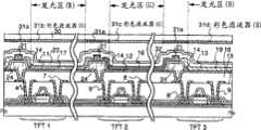
图2是EL模块的顶视图。在图中,在提供有许多TFT的衬底(也称为TFT衬底)之上,形成有用于显示器的象素部分40、用于驱动象素部分的象素的驱动电路41a和41b、用于连接在EL层上形成的电极和引线布线的连接部分、和用于与外围电路连接相连接的附加在FPC上的端子部分42。而且,采用密封EL元件和密封部件33的衬底以便获得一种密封状态。图1A是沿图2的虚线A-A`的剖面图。Fig. 2 is a top view of the EL module. In the figure, over a substrate provided with many TFTs (also referred to as a TFT substrate), there are formed a
在虚线A-A`方向上规则地排列象素。这里,将示出X方向上以R、G和B的次序排列的象素的例子。Pixels are regularly arranged in the direction of the dotted line A-A'. Here, an example of pixels arranged in the order of R, G, and B in the X direction will be shown.
在图1A中,发光区(R)表示发射红光的区域;发光区(G)表示发射绿光的区域;发光区(B)表示发射蓝光的区域。这些三种颜色的发光区实现了具有全色彩显示器能力的发光显示器。In FIG. 1A , the light-emitting region (R) represents a region that emits red light; the light-emitting region (G) represents a region that emits green light; and the light-emitting region (B) represents a region that emits blue light. These three-color light-emitting regions realize a light-emitting display with full-color display capability.
而且,在图1A中,TFT1是一个元件,该元件用于控制在发射红光的EL层17中流动的电流,并且参考数字4和7表示源电极或漏电极。此外,TFT2是一个元件,该元件用于控制在发射绿光的EL层18中流动的电流,并且参考数字5和8表示源电极或漏电极。TFT3是一个元件,该元件用于控制在发射蓝光的EL层19中流动的电流,并且参考数字6和9表示源电极或漏电极。参考数字15和16表示由有机绝缘材料或无机绝缘材料形成的层间绝缘膜。Also, in FIG. 1A, TFT1 is an element for controlling the current flowing in the
参考数字11-13每个表示有机发光元件的阳极(或阴极),参考数字20表示有机发光元件的阴极(或阳极)。在该例子中,阴极20由叠层膜制成,来自各个发光元件的光穿过阴极20,该叠层膜由薄金属层(典型地,MgAg、MgIn、AlLi等合金)和透明导电膜(氧化铟和氧化锡的合金(ITO)、氧化铟和氧化锌(In2O3-ZnO)合金、氧化锌(ZnO)等)组成。应当注意,提供透明导电膜不用作阴极而是降低电阻。作为阳极,可以采用下列材料:具有高功函数特别是铂(Pt)、铬(Cr)、钨(W)或镍(Ni)的材料;透明导电膜(ITO、ZnO等);以及它们的叠层膜。Reference numerals 11-13 each represent an anode (or cathode) of an organic light emitting element, and
此外,有机绝缘体24(也称为阻挡层或堤岸层)覆盖阳极(或阴极)11-13的两个端部和它们之间的部分。此外,有机绝缘体24覆盖有无机绝缘膜14。在每个有机绝缘体24上部分地形成有机化合物层。Furthermore, an organic insulator 24 (also referred to as a barrier layer or a bank layer) covers both ends of the anodes (or cathodes) 11-13 and a portion therebetween. Furthermore, the
在由无机绝缘膜14覆盖的有机绝缘体24(也称为阻挡层或堤岸层)上,形成辅助电极21。辅助电极21起降低阴极(或阳极)的电阻值的作用。上述透明导电膜具有相对的高电阻值,以致难于获得大的显示屏。但是,通过提供辅助电极21,用作阴极(或阳极)的电极可以降低作为整体的电阻。此外,可以降低透明导电膜的厚度。On an organic insulator 24 (also referred to as a barrier layer or a bank layer) covered with an inorganic insulating
此外,采用辅助电极21就可以获得与布线或较低层上的电极的连接。辅助电极21可以在形成EL层之前进行薄膜形成或图形化。辅助电极21可以通过溅射方法、蒸发方法等由掺杂有赋予一种导电类型的杂质元素的多晶硅、一种选自由W、WSix、Al、Ti、Mo、Cu、Ta、Cr和Mo组成的组的元素、主要含有主要含有该元素的合金材料或化合物材料的薄膜、或它们的叠层膜形成。因此,如果在辅助电极21上形成彼此接触的透明导电膜,该透明导电膜产生与较低层上的电极的接触,所以就可以引出阴极。应当注意,图1C是沿图2的虚线C-C`的剖面图。在图1C中,通过点线连接的电极彼此电连接。同样,在端子部分,端子的电极由与阴极10相同的材料形成。In addition, using the
此外,采用密封部件33将密封衬底30粘接其上以保持大约10μm的间隔,以致密封所有的发光元件。这里,需要将密封部件33变成具有小宽度的框架形状以便部分地重叠驱动电路。优选采用密封部件33将密封衬底30粘接其上之前立即在用于排除气体的真空室中进行密封。优选在含有氢气和惰性气体(稀有气体或氮)的环境中粘接密封衬底30并使由保护膜32、密封部件33和密封衬底30密封的空间含有氢气。利用发光元件发射光时产生的热使氢从含有氢的空间扩散,从而用氢终止有机化合物层中的缺陷。通过用氢终止有机化合物层中的缺陷,就可以提高发光器件的可靠性。In addition, the sealing
此外,为了提高色彩的纯度,在密封衬底30上提供与各个象素相对应的彩色滤光器。在彩色滤光器之中,与红光发射区(R)相对设置红颜色层31b,与绿光发射区(G)相对设置绿颜色层31c,与蓝光发射区(B)相对设置蓝颜色层31d。此外,除发光区域以外的区域由彩色滤光器的黑色部分屏蔽光,即光屏蔽部分31a。这里,光屏蔽部分31a由金属膜(含有铬等)或含有黑颜料的有机膜形成。In addition, color filters corresponding to the respective pixels are provided on the sealing
在本发明中,提供彩色滤光器就不需要圆形偏振平板。In the present invention, circular polarizing plates are not required to provide color filters.
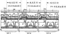
而且,图1B是沿图2的虚线B-B`的剖面图。此外在图1B中,无机绝缘膜14覆盖由11a-11c表示的部分的两个端部和之间的区域。在此情况下,尽管示出了一个例子,在该例子中通常采用EL层发射红光,但本发明并不特别地限制于上述结构。为用于发射相同颜色光的每个象素形成EL层同样是可能的。Moreover, FIG. 1B is a cross-sectional view along the dotted line BB' of FIG. 2 . Also in FIG. 1B, the inorganic insulating
此外,在图1A-1C中,形成保护膜32以提高发光器件的可靠性,该保护膜是主要含有氮化硅或氮氧化硅的绝缘膜并通过溅射方法形成。此外,在图1A-1C中,优选制造尽可能薄的保护膜以使发射的光穿过其中。In addition, in FIGS. 1A-1C , a
此外,为了提高发光器件的可靠性,在形成含有氢的薄膜之后形成保护膜32。在形成保护膜32之前通过形成含有氢的薄膜,终止在有机化合物层17-19中的缺陷。含有氢的薄膜可以是主要含有碳的薄膜或氮化硅膜。作为形成含有氢的薄膜的方法,通过等离子体CVD方法或溅射方法在有机化合物层可以承受的温度范围内形成该薄膜,例如,从室温到100℃或更低的范围。应当注意,在图1A-1C中,假定含有氢的薄膜部分地构成保护膜并因此在图中省略。含有氢的薄膜还可以用作缓冲层,该缓冲层用于释放保护膜32的薄膜应力。Furthermore, in order to improve the reliability of the light emitting device, the
不必进行说明,本发明不限制于图1C的结构。在图3A-3D中示出与图1C部分不同的结构的例子。这里,在图3A-3D中,为了简化用相同的符号表示与图1A-1C相同的部件。Needless to say, the present invention is not limited to the structure of FIG. 1C. An example of a structure partially different from that of FIG. 1C is shown in FIGS. 3A-3D. Here, in FIGS. 3A-3D , the same components as those in FIGS. 1A-1C are denoted by the same symbols for simplicity.
图1C示出一个例子,其中在端子部分设置由与阴极(透明电极)相同材料形成的电极。然而,图3A示出一个例子,其中采用由与TFT(W薄膜作为上层并且TaN薄膜作为下层)的栅电极相同材料形成的电极以获得与FPC的连接。FIG. 1C shows an example in which an electrode formed of the same material as a cathode (transparent electrode) is provided at the terminal portion. However, FIG. 3A shows an example in which an electrode formed of the same material as a gate electrode of a TFT (W film as an upper layer and a TaN film as a lower layer) is used to obtain connection to an FPC.
而且,图3B示出一个例子,其中采用由与象素电极(阳极)相同的材料形成的电极10以获得与FPC的连接。在此例子中,在由与TFT(W薄膜作为上层并且TaN薄膜作为下层)的栅电极相同材料制成的电极上彼此接触地形成电极10。Moreover, FIG. 3B shows an example in which an
图3C示出一个例子,其中用于获得与FPC连接的电极是由与阴极20(透明电极)相同的材料形成的电极,阴极20形成在与象素电极(阳极)相同的材料形成的电极10上,象素电极形成在TFT的引线布线上(在布线中以所述次序叠置TiN膜、Al膜和TiN膜)。3C shows an example in which the electrode used to obtain connection with the FPC is an electrode formed of the same material as the cathode 20 (transparent electrode), and the
图3D示出一个例子,其中用于获得与FPC连接的电极是由与阴极20(透明电极)相同材料形成的电极,阴极20形成在TFT的引线布线上(在布线中以所述次序叠置TiN膜、Al膜和TiN膜)。3D shows an example in which the electrode for obtaining connection with the FPC is an electrode formed of the same material as the cathode 20 (transparent electrode), which is formed on the lead wiring of the TFT (stacked in the stated order in the wiring) TiN film, Al film and TiN film).
[实施方式2][Embodiment 2]
这里,将参考图4A-4B描述含有氢的薄膜和保护膜。Here, the thin film containing hydrogen and the protective film will be described with reference to FIGS. 4A-4B .
图4A是示出EL元件的叠层结构例子的简图。在图4A中,参考数字200表示阴极(或阳极);201,表示EL层;202,表示阳极(或阴极);203,表示含有氢的DLC薄膜;204,表示保护膜。当发射的光穿过阳极202时,优选采用具有光透射特性(ITO、ZnO等)的导电膜作为阳极202。此外,优选采用金属膜(MgAg、MgIn、AlLi等的合金膜或通过铝和属于元素周期表中的1族或2族的元素共同蒸发形成的薄膜)或它们的叠层膜作为阴极200。Fig. 4A is a diagram showing an example of a laminated structure of an EL element. In FIG. 4A, reference numeral 200 denotes a cathode (or anode); 201, an EL layer; 202, an anode (or cathode); 203, a DLC film containing hydrogen; 204, a protective film. When emitted light passes through the anode 202, a conductive film having light transmission properties (ITO, ZnO, etc.) is preferably used as the anode 202. In addition, a metal film (an alloy film of MgAg, MgIn, AlLi, etc. or a thin film formed by co-evaporation of aluminum and an element belonging to
保护膜204可以由主要含有氮化硅或氮氧化硅的绝缘膜形成,通过溅射方法(DC系统或RF系统)获得该保护膜。可以通过采用硅靶在含有氮和氩的环境中形成获得氮化硅膜。此外,可以采用氮化硅靶。还可以通过采用远距离等离子体(remote plasma)的薄膜形成设备形成保护膜204。此外,当发射的光穿过保护膜时,优选制造尽可能薄的保护膜。The
含有氢的DLC膜203含有分别具有70-95原子%和5-30原子%组分的碳和氢,因此是非常硬并且具有优良的绝缘特性的薄膜。可以通过等离子体CVD方法(典型地,RF等离子体CVD方法、微波CVD方法、电子回旋共振(ECR)CVD方法等)、溅射方法等形成含有氢的DLC膜。The hydrogen-containing DLC film 203 contains carbon and hydrogen having compositions of 70-95 at% and 5-30 at%, respectively, and is therefore a very hard film having excellent insulating properties. The DLC film containing hydrogen can be formed by a plasma CVD method (typically, an RF plasma CVD method, a microwave CVD method, an electron cyclotron resonance (ECR) CVD method, etc.), a sputtering method, or the like.
作为形成含有氢的DLC膜203的方法,在有机化合物层可以承受的温度范围内形成该薄膜,例如从室温到100℃或更低的范围。As a method of forming the hydrogen-containing DLC film 203, the film is formed within a temperature range that the organic compound layer can withstand, for example, from room temperature to a range of 100° C. or lower.
当产生等离子体时作为用于薄膜形成的反应气体,可以采用氢气和碳氢基气体(例如,CH4、C2H2、C6H6等)。As a reaction gas for thin film formation when plasma is generated, hydrogen gas and hydrocarbon-based gas (for example, CH4 , C2 H2 , C6 H6 , etc.) can be used.
在有机化合物层可以承受的温度范围之内实施热处理并利用发光元件发射光产生的热,以致氢可以从含有氢的DLC膜扩散以便用氢终止有机化合物层中的缺陷(终止)。通过用氢终止有机化合物层中的缺陷,就可以提高发光元件的可靠性。同样,当形成含有氢的DLC膜时,可以利用转换为等离子体的氢用于用氢终止有机化合物层中的缺陷。此外,形成覆盖含有氢的DLC膜的保护膜用于阻挡朝保护膜一侧扩散的氢,并使氢有效地扩散进入有机化合物层以便用氢终止有机化合物层中的缺陷。应当注意,含有氢的DLC膜可以作为发光元件的保护膜。Heat treatment is performed within a temperature range that the organic compound layer can withstand and utilizes heat generated by light emitted from the light emitting element so that hydrogen can diffuse from the DLC film containing hydrogen to terminate defects in the organic compound layer with hydrogen (termination). By terminating defects in the organic compound layer with hydrogen, the reliability of the light-emitting element can be improved. Also, when forming a DLC film containing hydrogen, hydrogen converted to plasma can be utilized for terminating defects in the organic compound layer with hydrogen. In addition, a protective film covering the DLC film containing hydrogen is formed to block hydrogen diffused toward the protective film side, and to efficiently diffuse hydrogen into the organic compound layer to terminate defects in the organic compound layer with hydrogen. It should be noted that the DLC film containing hydrogen can serve as a protective film of the light emitting element.
此外,含有氢的DLC膜的可以作为缓冲层。当通过溅射方法形成与由透明导电膜制造的薄膜接触的氮化硅膜时,就有可能将在透明导电膜中含有的杂质(In、Sn、Zn等)混合进入氮化硅膜。然而,通过形成含有氢的DLC膜作为其间的缓冲层,还能够防止杂质的混合物进入氮化硅膜。根据上述结构,形成缓冲层,以致可以防止杂质(In、Sn、Zn等)从透明导电膜混入,并可以形成没有杂质的优良的保护膜。In addition, the DLC film containing hydrogen can serve as a buffer layer. When a silicon nitride film in contact with a thin film made of a transparent conductive film is formed by a sputtering method, there is a possibility that impurities (In, Sn, Zn, etc.) contained in the transparent conductive film are mixed into the silicon nitride film. However, by forming a DLC film containing hydrogen as a buffer layer therebetween, it is also possible to prevent a mixture of impurities from entering the silicon nitride film. According to the above structure, the buffer layer is formed so that impurities (In, Sn, Zn, etc.) can be prevented from being mixed from the transparent conductive film, and an excellent protective film free from impurities can be formed.
具有这种结构,就能够提高可靠性并且更好地保护发光元件。With such a structure, reliability can be improved and the light emitting element can be better protected.
此外,图4B是示出EL元件的叠层结构的另一个例子的简图。在图4B中,参考数字400表示阴极(或阳极);301,表示EL层;302,表示阳极(或阴极);303,表示含有氢的氮化硅膜;304,表示保护膜。当发射的光穿过阳极302时,优选采用具有光透射特性的导电材料、非常薄的金属膜(MgAg)或它们的叠层膜形成阳极302。In addition, FIG. 4B is a diagram showing another example of the laminated structure of the EL element. In FIG. 4B, reference numeral 400 denotes a cathode (or anode); 301, an EL layer; 302, an anode (or cathode); 303, a silicon nitride film containing hydrogen; and 304, a protective film. When emitted light passes through the anode 302, it is preferable to form the anode 302 using a conductive material having light-transmitting properties, a very thin metal film (MgAg), or a laminated film thereof.
此外,当发射的光穿过阳极302时,优选采用具有光透射特性的导电膜(ITO、ZnO等)作为阳极302。此外,优选采用金属膜(MgAg、MgIn、AlLi等的合金膜或通过铝和属于元素周期表中的1或2族的元素共同蒸发形成的薄膜)或它们的叠层膜作为阴极300。In addition, when emitted light passes through the anode 302 , it is preferable to use a conductive film (ITO, ZnO, etc.) having light-transmitting characteristics as the anode 302 . In addition, it is preferable to use a metal film (alloy film of MgAg, MgIn, AlLi, etc. or a thin film formed by co-evaporation of aluminum and elements belonging to
保护膜304可以由主要含有氮化硅或氧氮化硅的绝缘膜形成,通过溅射方法(DC系统或RF系统)获得该保护膜。可以通过采用硅靶在含有氮和氩的环境中形成获得氮化硅膜。此外,可以采用氮化硅靶。还可以通过采用远距离等离子体的薄膜形成设备形成保护膜304。此外,当发射的光穿过保护膜时,优选制造尽可能薄的保护膜。The protective film 304 may be formed of an insulating film mainly containing silicon nitride or silicon oxynitride, which is obtained by a sputtering method (DC system or RF system). The silicon nitride film can be obtained by forming in an atmosphere containing nitrogen and argon using a silicon target. In addition, silicon nitride targets may be used. The protective film 304 can also be formed by a thin film forming apparatus using remote plasma. Furthermore, when emitted light passes through the protective film, it is preferable to make the protective film as thin as possible.
可以通过等离子体CVD方法(典型地,RF等离子体CVD方法、微波CVD方法、电子回旋共振(ECR)CVD方法等)、RF溅射方法、DC溅射方法等形成含氢的氮化硅膜303。The hydrogen-containing silicon nitride film 303 can be formed by a plasma CVD method (typically, an RF plasma CVD method, a microwave CVD method, an electron cyclotron resonance (ECR) CVD method, etc.), an RF sputtering method, a DC sputtering method, or the like. .
作为形成含氢的氮化硅膜303的方法,在有机化合物层可以承受的温度范围内形成该薄膜,例如从室温到100℃或更低的范围。As a method of forming the hydrogen-containing silicon nitride film 303, the film is formed within a temperature range that the organic compound layer can withstand, for example, from room temperature to a range of 100° C. or lower.
当采用等离子体CVD方法作为用于含有氢的氮化硅膜303的形成方法时,可以采用含有氮的气体(由N2和NH3NOX等表示的氮氧化物基气体)和氢硅化物基气体(例如,硅烷(SiH4)、乙硅烷、丙硅烷等)作为反应气体。When the plasma CVD method is employed as the formation method for the hydrogen-containing silicon nitride film 303, nitrogen-containing gas (nitrogen oxide-based gas represented by N2 and NH3 NOX , etc.) and hydrogen silicide can be used. A base gas (for example, silane (SiH4 ), disilane, trisilane, etc.) is used as the reaction gas.
当采用溅射方法作为形成含有氢的氮化硅膜303的方法时,可以采用硅靶在含有氢、氮和氩的环境中通过形成获得含有氢的氮化硅膜。此外,可以采用氮化硅靶。When a sputtering method is employed as a method of forming the hydrogen-containing silicon nitride film 303, the hydrogen-containing silicon nitride film can be obtained by formation using a silicon target in an atmosphere containing hydrogen, nitrogen, and argon. In addition, silicon nitride targets may be used.
在有机化合物层可以承受的温度范围之内实施热处理并利用发光元件发射光产生的热,以致氢可以从含有氢的氮化硅膜扩散以用氢终止有机化合物层中的缺陷(消除)。通过用氢终止有机化合物层中的缺陷,就提高发光元件的可靠性。同样,当形成含有氢的氮化硅膜时,可以利用转换为等离子体的氢以便用氢终止有机化合物层中的缺陷。此外,形成覆盖含有氢的氮化硅膜的保护膜用于阻挡朝保护膜一侧扩散的氢,并使氢有效地扩散进入有机化合物层以便用氢终止有机化合物层中的缺陷。应当注意,含有氢的氮化硅膜还可以作为发光元件的保护膜。Heat treatment is performed within a temperature range that the organic compound layer can withstand and utilizes heat generated by light emitted from the light emitting element so that hydrogen can diffuse from the silicon nitride film containing hydrogen to terminate (eliminate) defects in the organic compound layer with hydrogen. By terminating defects in the organic compound layer with hydrogen, the reliability of the light emitting element is improved. Also, when forming a silicon nitride film containing hydrogen, hydrogen converted to plasma can be utilized to terminate defects in the organic compound layer with hydrogen. In addition, a protective film covering the hydrogen-containing silicon nitride film is formed to block hydrogen diffused toward the protective film side, and to efficiently diffuse hydrogen into the organic compound layer to terminate defects in the organic compound layer with hydrogen. It should be noted that the hydrogen-containing silicon nitride film can also serve as a protective film for the light emitting element.
此外,含有氢的氮化硅膜可以作为缓冲层。当通过溅射方法形成与由透明导电膜制造的薄膜接触的氮化硅膜时,就有可能将在透明导电膜中含有的杂质(In、Sn、Zn等)混合进入氮化硅膜。然而,通过形成含有氢的氮化硅膜作为其间的缓冲层,还有可能防止杂质的混合物进入氮化硅膜。根据上述结构,形成缓冲层,以致可以防止杂质(In、Sn等)从透明导电膜混入,并可以形成没有杂质的优良的保护膜。In addition, a silicon nitride film containing hydrogen can be used as a buffer layer. When a silicon nitride film in contact with a thin film made of a transparent conductive film is formed by a sputtering method, there is a possibility that impurities (In, Sn, Zn, etc.) contained in the transparent conductive film are mixed into the silicon nitride film. However, it is also possible to prevent a mixture of impurities from entering the silicon nitride film by forming a silicon nitride film containing hydrogen as a buffer layer therebetween. According to the above structure, the buffer layer is formed so that impurities (In, Sn, etc.) can be prevented from being mixed from the transparent conductive film, and an excellent protective film free from impurities can be formed.
具有上述结构,就能够提高可靠性并可以保护发光元件。With the above structure, reliability can be improved and the light emitting element can be protected.
而且,图4A-4B示出一个例子,其中提供含有氢的薄膜作为单层,但是薄膜可以是由含有氢的氮化硅膜和含有氢的DLC膜组成的叠层或它们的具有三层或多层的叠层。Also, FIGS. 4A-4B show an example in which a hydrogen-containing thin film is provided as a single layer, but the thin film may be a laminate composed of a hydrogen-containing silicon nitride film and a hydrogen-containing DLC film or a combination thereof having three layers or Lamination of multiple layers.
此外,不仅可以应用本实施方式到有源矩阵显示器件而且可以应用于无源显示器件。Furthermore, this embodiment mode can be applied not only to active matrix display devices but also to passive display devices.
而且,本实施方式可以与实施方式1自由地结合。Also, this embodiment mode can be freely combined with
[实施方式3][Embodiment 3]
这里,图6A-6C示出部分不同于图1A-1C的结构的例子。在本例子中,将在下面利用例子描述本发明,即在象素部分中规则地排列的许多象素中,采用3×3矩阵中的象素。应当注意,在剖面结构中,图6A-6C的TFT基本上与图1A-1C的TFT一样,因此为了简化采用相同的参考数字表示与图1A-1C中的相同的部件。Here, FIGS. 6A-6C show examples of structures that are partially different from FIGS. 1A-1C. In this example, the present invention will be described below using an example in which pixels in a 3x3 matrix are used among a plurality of pixels regularly arranged in the pixel portion. It should be noted that in the cross-sectional structure, the TFT of FIGS. 6A-6C is substantially the same as the TFT of FIGS. 1A-1C, and therefore the same reference numerals are used to designate the same components as those in FIGS. 1A-1C for simplicity.
图6A是沿图5A的长和短间隔的虚线A-A`的剖面图。发光区50R表示红色光发射区;发光区50G,表示绿色光发射区;发光区50B,表示蓝色光发射区。三种颜色的这些发光区实现了具有全彩色显示器能力的发光显示器件。Fig. 6A is a cross-sectional view along the long and short dashed line A-A' of Fig. 5A. The
如图6A所示,本实施方式采用一个例子,其中采用相同的掩模进行图形化。因此,从上面观察,辅助电极621和有机绝缘体624基本上具有相同的形状。在此情况下,如图6C所示,辅助电极621通过阴极20电连接到与源极布线相同的材料制造的布线。As shown in FIG. 6A, this embodiment mode takes an example in which patterning is performed using the same mask. Therefore, the
而且,在层间绝缘膜15上形成象素电极612(612a-612c)并在形成象素电极612之后形成TFT的接触孔,通过该接触孔随后形成的电极607和608电连接象素电极612和TFT。无机绝缘膜14覆盖象素电极的两个端部和象素电极之间的部分。同样,与图1A-1C类似,形成有机化合物层以便部分地覆盖有机绝缘体624。Also, a pixel electrode 612 (612a-612c) is formed on the
图5B是示出刚刚在形成象素电极之后的象素电极的顶视图,其对应于图5A。在图5A和5B中,提供有机化合物层用于每个象素的列(Y方向)。在有机化合物层之间提供条形形状的有机绝缘体624,有机化合物在条形形状中发出的光的颜色彼此不同。此外,在图5A中,提供有机绝缘体624和辅助电极621用于每个象素的列(Y方向)。FIG. 5B is a top view showing a pixel electrode immediately after forming the pixel electrode, which corresponds to FIG. 5A. In FIGS. 5A and 5B, an organic compound layer is provided for each pixel column (Y direction). The
图7A是相应于图5A-6C的顶视图。在图7A中,剖面图中左手部分的连接部分部分地示出在右手部分中,它对应于图6C中所示的部分。此外,当对图7A的辅助电极621和有机绝缘体进行图形化时,采用图8A中所示的金属掩模作为例子。Figure 7A is a top view corresponding to Figures 5A-6C. In FIG. 7A, the connecting portion of the left-hand portion in the sectional view is partially shown in the right-hand portion, which corresponds to the portion shown in FIG. 6C. In addition, when patterning the
而且,当有机绝缘体和辅助电极的总的薄膜厚度比较大时,就增加了台阶,因此就可能难于采用透明导电膜用于电连接。特别地,在透明导电膜制造得薄的情况下,由于劣质的覆盖就会发生线缺陷。因此,如图7B所示,为了进一步确保辅助电极621和较低层上的电极之间的连接,可以增加掩模的数量以形成622表示的电极。同样,可以采用金属掩模以便通过蒸发方法形成电极622。Also, when the total film thickness of the organic insulator and the auxiliary electrode is relatively large, steps are increased, so it may be difficult to use a transparent conductive film for electrical connection. In particular, in the case where the transparent conductive film is made thin, line defects occur due to poor coverage. Therefore, as shown in FIG. 7B , in order to further ensure the connection between the
此外,如图7C中所示,预先形成由与源极布线相同材料制造的布线623以便环绕象素部分。随后,可以形成第二辅助电极624以便直角地与辅助电极621相交。具有这种排列,可以提供每个第二辅助电极624以便直接地接触布线623以及辅助电极621。这里,设计辅助电极621和第二辅助电极624,使得它们之间的部分可以适合地作为发光区。同样,当对图7A的第二辅助电极624进行图形化时,可以采用作为例子的图8B中所示的金属掩模。Furthermore, as shown in FIG. 7C, a
此外,图7C示出一个例子,其中,进行两次图形化以形成第一辅助电极621和第二辅助电极624。然而,可以采用图8C中所示的金属掩模可以网格形状形成辅助电极。如图8C的右手部分所示,沿细线分割开口。当蒸发时,出现局部使薄膜变薄的环绕部分,但可以以网格形状形成辅助电极。In addition, FIG. 7C shows an example in which patterning is performed twice to form the first
同样,本实施方式可以与实施方式1或2自由地结合。Also, this embodiment mode can be freely combined with
[实施方式4][Embodiment 4]
这里,图9A-9C中示出部分地与图1A-1C中不同的结构的例子。在此例子中,将在下面利用例子描述本发明,即在象素部分中规则地排列的许多象素中,采用3×3矩阵中的象素。应当注意,在剖面结构中,除了不提供有机绝缘体24并在整个表面上提供聚合物制造的有机化合物层60之外,该结构基本上与图1A-1C的结构基本一样。因此,图9A-9C中,为了简化采用相同的参考数字表示与图1A-1C中相同的部件。此外,图9A是沿图2A的虚线A-A`的剖面图。Here, examples of structures partially different from those in FIGS. 1A-1C are shown in FIGS. 9A-9C . In this example, the present invention will be described below using an example in which pixels in a 3 x 3 matrix are used among a plurality of pixels regularly arranged in the pixel portion. It should be noted that, in the cross-sectional structure, the structure is basically the same as that of FIGS. 1A-1C except that the
图9A-9C的结构中提供替代图1A-1C中所示的有机绝缘体24,无机绝缘膜14和辅助电极721用作维持有机化合物17、18和19之间的间隔。In the structure of FIGS. 9A-9C , instead of the
而且,通过涂覆方法例如旋涂方法或喷涂方法形成并由此在整个表面上形成由聚合物(作为参考,典型地,聚(亚乙基二氧基噻吩)/聚(苯乙烯磺酸酯)水溶液(此后称为“PEDOT/PSS”)作为空穴注入层)制造的有机化合物层60。同样,由聚合物制造的有机化合物层60具有导电性,通过有机化合物层60就获得了阴极20和辅助电极721之间的电连接。通过提供辅助电极721,可以降低阴极(或阳极)的整体电阻。此外,可以将透明导电膜制造得薄。此外,采用辅助电极721以获得与布线或较低层中的电极的连接。在形成EL层之前,可以进行薄膜的形成或图形化辅助电极721。如果在辅助电极721上形成透明导电膜并与较低层中的电极的接触,就能够引出阴极。应当注意,图9C是沿图2的虚线C-C`的剖面图。此外,在图9C中,通过虚线连接的电极彼此电连接。在端子部分中,由与阴极20相同材料形成端子的电极。Furthermore, it is formed by a coating method such as a spin coating method or a spray coating method and thus is formed on the entire surface by a polymer (for reference, typically, poly(ethylenedioxythiophene)/poly(styrenesulfonate) ) aqueous solution (hereinafter referred to as "PEDOT/PSS") as a hole injection layer)
此外,图9B是沿图2的虚线B-B`的剖面图。同样在图9B中,无机绝缘膜14覆盖由11a-11c表示的部分的两个端部和它们之间的区域。在此情况下,尽管示出了一个例子,其中通常采用发射红光的EL层17,本发明并不具体地限制于上述结构。还可以形成EL层用于发射相同颜色的每个象素。In addition, FIG. 9B is a cross-sectional view along the dotted line BB' of FIG. 2 . Also in FIG. 9B, the inorganic insulating
此外,本实施方式可以与实施方式1至实施方式3之一自由地组合。In addition, this embodiment mode can be freely combined with one of
[实施方式5][Embodiment 5]
这里,图10A-10C中示出部分地与图1A-1C中不同结构的例子。在此例子中,将在下面利用例子描述本发明,即在象素部分中规则地排列的许多象素中,采用3×3矩阵中的象素。应当注意,在剖面图中,除了在阴极20上提供辅助电极821之外,该结构基本上与图1A-1C的结构一样。因此,图10A-10C中,为了简化采用相同的参考数字表示与图1A-1C中相同的部件。此外,图10A是沿图2的虚线A-A`的剖面图。Here, examples of structures partially different from those in FIGS. 1A-1C are shown in FIGS. 10A-10C. In this example, the present invention will be described below using an example in which pixels in a 3 x 3 matrix are used among a plurality of pixels regularly arranged in the pixel portion. It should be noted that, in cross-section, the structure is substantially the same as that of FIGS. 1A-1C except that an
而且,在阴极上形成并通过蒸发方法采用金属掩模形成辅助电极821。在此情况下,其中以栅格形状形成辅助电极821的例子。通过提供辅助电极821,就可以降低阴极(或阳极)的整体电阻。此外,可以将透明导电膜制造得薄。此外,采用辅助电极821以获得与布线或较低层中的电极的连接。如果在辅助电极821上形成透明导电膜产生与较低层中的电极的接触,就能够引出阴极。应当注意,图10C是沿图2的虚线C-C`的剖面图。此外,在图10C中,通过点线连接的电极彼此电连接。在端子部分中,由与阴极20相同材料形成端子的电极。Also, an
此外,本实施方式可以与实施方式1至实施方式4之一自由地组合。In addition, this embodiment mode can be freely combined with one of
因此,将采用下面的实施例进一步详细地描述本发明的结构。Therefore, the structure of the present invention will be described in further detail using the following examples.
[实施例1][Example 1]
在本实施例中,描述在绝缘表面上形成的有源矩阵型发光器件。这里采用薄膜晶体管(此后称为TFT)作为有源元件,还可以采用MOS晶体管。In this embodiment, an active matrix type light emitting device formed on an insulating surface is described. Here, thin film transistors (hereinafter referred to as TFTs) are used as active elements, and MOS transistors may also be used.
示出顶栅电极TFT(特别是平面TFT)作为一个例子,也可以采用底栅电极TFT(典型地为反向交错的TFT)。While a top-gate TFT (particularly a planar TFT) is shown as an example, a bottom-gate TFT (typically an inverted staggered TFT) may also be used.
在本实施例中,采用玻璃衬底,该玻璃衬底由硼硅酸钡玻璃或硼硅酸铝玻璃制成,可以采用石英衬底、硅衬底、在其表面上形成绝缘膜的金属衬底或不锈钢衬底。也可以采用具有能承受本实施例的处理温度的耐热塑料衬底,此外可以采用柔性衬底。In this embodiment, a glass substrate is used. The glass substrate is made of barium borosilicate glass or aluminoborosilicate glass. A quartz substrate, a silicon substrate, a metal substrate on which an insulating film is formed may be used. Bottom or stainless steel substrate. A heat-resistant plastic substrate having a temperature capable of withstanding the processing of this embodiment can also be used, and a flexible substrate can also be used.
随后,通过等离子体CVD在400℃的温度下采用SiH4、NH3和N2O作为材料气体(组分比:Si=32%,O=27%,N=24%,H=17%)在0.7mm厚度的耐热玻璃衬底上形成氧氮化硅膜作为基底绝缘膜的下层。氧氮化硅膜具有50nm的厚度(优选10-200nm)。用双氧水冲洗薄膜的表面,然后用稀释的氟酸(稀释到1/100)去除表面上的氧化膜。随后,通过等离子体CVD、在400℃的温度下、采用SiH4和N2O作为材料气体(组分比:Si=32%,O=59%,N=7%,H=2%)形成氧氮化硅膜作为基底绝缘膜的上层。氧氮化硅膜具有100nm的厚度(优选50-200nm)并位于下层之上以形成叠层。不将叠层暴露到空气中,通过等离子体CVD、在300℃的温度下、采用SiH4作为材料气体在叠层上形成具有非晶结构(这里,非晶硅膜)的半导体膜。半导体膜(这里,采用非晶硅膜)为54nm的厚度(优选25-200nm)。Subsequently, SiH4 , NH3 and N2 O were used as material gases at a temperature of 400° C. by plasma CVD (composition ratio: Si=32%, O=27%, N=24%, H=17%) A silicon oxynitride film was formed as a lower layer of the base insulating film on a heat-resistant glass substrate with a thickness of 0.7 mm. The silicon oxynitride film has a thickness of 50 nm (preferably 10-200 nm). Rinse the surface of the film with hydrogen peroxide, and then use diluted hydrofluoric acid (diluted to 1/100) to remove the oxide film on the surface. Subsequently, it was formed by plasma CVD at a temperature of 400°C using SiH4 and N2 O as material gases (composition ratio: Si=32%, O=59%, N=7%, H=2%) A silicon oxynitride film is used as an upper layer of the base insulating film. The silicon oxynitride film has a thickness of 100 nm (preferably 50 to 200 nm) and is placed on the lower layer to form a stack. Without exposing the stack to the air, a semiconductor film having an amorphous structure (here, an amorphous silicon film) was formed on the stack by plasma CVD at a temperature of 300° C. using SiH4 as a material gas. The semiconductor film (here, an amorphous silicon film is used) has a thickness of 54 nm (preferably 25-200 nm).
本实施例中的基底绝缘膜具有两层结构。然而,基底绝缘膜可以是主要含有硅的绝缘膜的单层或比两层更多的层。半导体膜的材料不限于但优选从硅或硅锗合金(SiXGe1-X(X=0.0001-0.02))中通过已知方法(溅射、LPCVD、等离子体CVD等)形成半导体膜。采用的等离子体CVD设备可以是一个晶片接着一个晶片地处理的一种设备或批量处理的一种设备。可以连续地在相同的室中形成基底绝缘膜和半导体膜以避免接触空气。The base insulating film in this embodiment has a two-layer structure. However, the base insulating film may be a single layer or more than two layers of an insulating film mainly containing silicon. The material of the semiconductor film is not limited but is preferably formed from silicon or a silicon-germanium alloy (SiX Ge1-X (X=0.0001-0.02)) by a known method (sputtering, LPCVD, plasma CVD, etc.). The plasma CVD apparatus employed may be one for wafer-by-wafer processing or one for batch processing. The base insulating film and the semiconductor film can be successively formed in the same chamber to avoid contact with air.
冲洗具有非晶结构的半导体膜的表面,然后采用双氧水在表面上形成大约2nm厚度的非常薄的氧化膜。随后,为了控制TFT的阈值电压,用微量杂质元素(硼或磷)掺杂半导体膜。这里,通过离子掺杂用硼掺杂非晶硅膜,在离子掺杂中通过等离子体而不用质量分离激活乙硼烷(B2H6)。掺杂条件包括设置15kV的加速电压、通过用氢气将乙硼烷稀释到1%而获得的30sccm的气体流速、以及剂量到2×10¹²atoms/cm2(原子/平方厘米)。The surface of the semiconductor film having an amorphous structure is rinsed, and then a very thin oxide film with a thickness of about 2 nm is formed on the surface using hydrogen peroxide. Subsequently, in order to control the threshold voltage of the TFT, the semiconductor film is doped with a trace amount of impurity element (boron or phosphorus). Here, the amorphous silicon film is doped with boron by ion doping in which diborane (B2 H6 ) is activated by plasma without mass separation. The doping conditions included setting an accelerating voltage of 15 kV, a gas flow rate of 30 sccm obtained by diluting diborane to 1% with hydrogen, and a dose to 2×10¹² atoms/cm2 (atoms/square centimeter).
随后,通过旋涂机提供含有重量比为10ppm镍的乙酸镍溶液。替代涂敷,可以通过溅射将镍喷射到整个表面上。Subsequently, a nickel acetate solution containing nickel in a weight ratio of 10 ppm was supplied by a spin coater. Instead of coating, nickel can be sprayed onto the entire surface by sputtering.
进行半导体膜热处理以晶化它并获得具有晶体结构的半导体膜。在电炉中或通过强光的辐射完成热处理。当在电炉中实施热处理时,温度设置到500-650℃,热处理持续4-24小时。这里,在脱氢作用(500℃下、1小时)的热处理之后,通过用于结晶化的热处理(550℃下、4小时)获得具有晶体结构的硅膜。尽管这里通过热处理采用电炉结晶化半导体膜,可以通过能够在短时间内完成结晶化的灯退火设备进行晶化。Heat treatment of the semiconductor film is performed to crystallize it and obtain a semiconductor film having a crystal structure. Heat treatment is done in an electric furnace or by irradiation with intense light. When the heat treatment is carried out in an electric furnace, the temperature is set to 500-650° C., and the heat treatment lasts for 4-24 hours. Here, after heat treatment for dehydrogenation (at 500°C, 1 hour), a silicon film having a crystal structure is obtained by heat treatment for crystallization (at 550°C, for 4 hours). Although the electric furnace is used to crystallize the semiconductor film by heat treatment here, crystallization can be performed by lamp annealing equipment capable of completing crystallization in a short time.
在通过稀释的氟酸等去除具有晶体结构的硅膜的表面上的氧化膜之后,为了获得大晶粒尺寸的晶体,当晶化非晶硅膜时采用连续波固态激光器和基波的二次至四次谐波。由于在空气或在氧化气氛中进行激光辐照,结果会在表面上形成氧化膜。典型地,采用Nd:YVO4激光器(基波:1064nm)的二次谐波(532nm)或三次谐波(355nm)。当采用连续波激光器时,由10W功率的连续波YVO4激光器发射的激光通过非线性光学元件被转换为谐波。或者,通过在共振器中设置YVO4晶体和非线性光学元件获得谐波。通过光学系统在辐照表面上的谐波优选被变形为长方形或椭圆形的激光,然后辐射辐照的物体。此时需要的能量密度为大约0.01-100MW/cm2(优选0.1-10MW/cm2)。在辐照期间,相对于激光以10-2000cm/s的速度移动半导体膜。After removing the oxide film on the surface of the silicon film having a crystal structure by dilute hydrofluoric acid, etc., in order to obtain a crystal with a large grain size, a continuous wave solid-state laser and a secondary of the fundamental wave are used when crystallizing the amorphous silicon film to the fourth harmonic. As a result of laser irradiation in air or in an oxidizing atmosphere, an oxide film is formed on the surface. Typically, the second harmonic (532 nm) or third harmonic (355 nm) of a Nd:YVO4 laser (fundamental: 1064 nm) is used. When a continuous wave laser is used, the laser light emitted by a continuous wave YVO4 laser with a power of 10W is converted to harmonics by a nonlinear optical element. Alternatively, harmonics are obtained by placing a YVO4 crystal and nonlinear optical elements in the resonator. The harmonics on the irradiated surface are preferably deformed by the optical system into rectangular or elliptical laser light, which then irradiates the irradiated object. The required energy density at this time is about 0.01-100 MW/cm2 (preferably 0.1-10 MW/cm2 ). During irradiation, the semiconductor film is moved at a speed of 10-2000 cm/s relative to the laser light.
当然,尽管在其上辐照连续波YVO4激光器的二次谐波之前可以通过采用具有结晶化结构的硅膜形成TFT,由于其上辐照激光的硅膜具有改善的结晶度并提高TFT的电特性,因此优选采用在其上辐照激光之后具有结晶化结构的硅膜以形成TFT。例如,尽管,参与在其上辐照激光之前通过具有结晶化结构的硅膜形成TFT,迁移率几乎为300cm2/Vs;当通过采用在其上辐照激光之后具有结晶化结构的硅膜形成TFT时,迁移率极大地提高为大约500-600cm2/Vs。Of course, although the TFT can be formed by using a silicon film having a crystallized structure before irradiating the second harmonic of the continuous wave YVO4 laser thereon, since the silicon film on which the laser is irradiated has improved crystallinity and improves the TFT electrical characteristics, it is therefore preferable to use a silicon film having a crystallized structure after irradiating laser light thereon to form a TFT. For example, although, participating in forming a TFT by a silicon film having a crystallized structure before irradiating laser light thereon, the mobility is almost 300 cm2 /Vs; when formed by using a silicon film having a crystallized structure after irradiating laser light thereon In TFT, the mobility is greatly improved to about 500-600 cm2 /Vs.
在采用镍作为加速硅的结晶化的金属元素进行结晶化之后,在其上辐照连续波YVO4激光器的二次谐波,并不限制于此,在形成具有非晶结构的硅膜之后,进行脱氢的热处理,通过辐照连续波YVO4激光器的二次谐波可以获得具有晶体结构的硅膜。After crystallization using nickel as a metal element to accelerate the crystallization of silicon, the second harmonic wave of a continuous wave YVO4 laser is irradiated thereon, not limited thereto, and after forming a silicon film having an amorphous structure, A heat treatment for dehydrogenation is performed, and a silicon film with a crystalline structure can be obtained by irradiating the second harmonic of a continuous wave YVO4 laser.
可以采用脉冲波激光器来替代连续波激光器。在采用脉冲波的受激准分子激光器的情况下,优选频率设置为300Hz,激光密度设置为从100-1000mJ/cm2(典型地200-800mJ/cm2)。这里,激光可以重叠50-98%。A pulsed wave laser can be used instead of a continuous wave laser. In the case of an excimer laser employing a pulse wave, it is preferable that the frequency is set to 300 Hz and the laser density is set from 100-1000 mJ/cm2 (typically 200-800 mJ/cm2 ). Here, the lasers can overlap by 50-98%.
除了通过激光辐照形成的氧化膜之外,用双氧水处理表面120秒以形成作为阻挡层的具有总厚度为1-5nm的氧化膜。这里采用双氧水形成阻挡层,但也可以在氧气环境中通过紫外光辐照氧化具有晶体结构的半导体膜的表面形成它,或者通过氧等离子体处理氧化具有晶体结构的半导体膜的表面形成它,或通过采用等离子体CVD、溅射或蒸发以形成大约1-10nm厚度的氧化膜。在形成阻挡层之前,可以去除通过激光辐照形成的氧化膜。In addition to the oxide film formed by laser irradiation, the surface was treated with hydrogen peroxide for 120 seconds to form an oxide film having a total thickness of 1-5 nm as a barrier layer. Here, hydrogen peroxide is used to form the barrier layer, but it can also be formed by oxidizing the surface of the semiconductor film with a crystal structure by ultraviolet light irradiation in an oxygen environment, or oxidizing the surface of a semiconductor film with a crystal structure by oxygen plasma treatment, or An oxide film with a thickness of about 1-10 nm is formed by using plasma CVD, sputtering or evaporation. Before forming the barrier layer, the oxide film formed by laser irradiation may be removed.
随后,通过等离子体CVD或溅射在阻挡层上形成含有氩的非晶硅膜以便用作吸杂的位置(gettering site)。非晶硅膜的厚度为50-400nm,这里是150nm。在氩环境中、通过溅射、采用硅靶、薄膜形成压力为0.3Pa下形成非晶硅膜。Subsequently, an amorphous silicon film containing argon is formed on the barrier layer by plasma CVD or sputtering to serve as a gettering site. The thickness of the amorphous silicon film is 50-400 nm, here 150 nm. An amorphous silicon film was formed in an argon atmosphere by sputtering using a silicon target at a film forming pressure of 0.3 Pa.
此后,在电炉中、650℃下、3分钟下进行吸杂的热处理以便降低具有晶体结构的半导体膜中的镍浓度。可以采用灯退火设备来替代电炉。Thereafter, heat treatment of gettering was performed in an electric furnace at 650° C. for 3 minutes in order to reduce the nickel concentration in the semiconductor film having a crystal structure. Lamp annealing equipment can be used instead of an electric furnace.
采用阻挡层作为蚀刻停止层,选择去除吸杂位置,就是说含有氩的非晶硅膜。然后,通过稀释的氟酸选择去除阻挡层。在吸杂期间镍移动趋向具有高的氧浓度的区域,因此在吸杂之后需要去除氧化膜的阻挡层。Using a barrier layer as an etch stop layer, the gettering sites are selectively removed, that is, the argon-containing amorphous silicon film. Then, the barrier layer is selectively removed by dilute hydrofluoric acid. Nickel moves toward a region with a high oxygen concentration during gettering, so it is necessary to remove the barrier layer of the oxide film after gettering.
随后,采用双氧水在获得的含有晶体结构的硅膜(也称为多晶硅膜)的表面上形成薄氧化膜。然后形成抗蚀剂掩模并腐蚀硅膜以形成彼此分开的并具有所需形状的岛型半导体层。在形成半导体层之后,去除抗蚀剂掩模。Subsequently, a thin oxide film was formed on the surface of the obtained silicon film containing a crystal structure (also referred to as a polysilicon film) using hydrogen peroxide. A resist mask is then formed and the silicon film is etched to form island-type semiconductor layers separated from each other and having a desired shape. After forming the semiconductor layer, the resist mask is removed.
通过含有氟酸的蚀刻剂去除氧化膜,同时清洗硅膜的表面。然后,形成主要含有硅的绝缘膜作为栅绝缘膜。这里栅绝缘膜是通过等离子体CVD形成的具有115nm厚度的氧氮化硅膜(组分比:Si=32%,O=59%,N=7%,H=2%)。The surface of the silicon film is cleaned while removing the oxide film with an etchant containing hydrofluoric acid. Then, an insulating film mainly containing silicon is formed as a gate insulating film. Here the gate insulating film is a silicon oxynitride film (composition ratio: Si = 32%, O = 59%, N = 7%, H = 2%) formed by plasma CVD with a thickness of 115 nm.
随后,在栅绝缘膜上形成厚度为20-100nm的第一导电膜和厚度为100-400nm的第二导电膜的叠层。在本实施例中,在栅绝缘膜上形成50nm厚度的氮化钽膜,然后在其上叠放370nm厚度的钨膜。通过下面示出的工序图形化导电膜以形成栅电极和布线。Subsequently, a stack of a first conductive film having a thickness of 20-100 nm and a second conductive film having a thickness of 100-400 nm is formed on the gate insulating film. In this embodiment, a tantalum nitride film with a thickness of 50 nm is formed on the gate insulating film, and a tungsten film with a thickness of 370 nm is stacked thereon. The conductive film is patterned by the procedure shown below to form gate electrodes and wirings.
第一导电膜和第二导电膜的导电材料是选自由Ta、W、Ti、Mo、Al和Cu组成的一组的元素、或主要含有上述元素的合金或化合物。第一导电膜和第二导电膜可以是半导体膜,典型地为掺杂有磷或其它杂质元素的多晶硅膜,或可以是Ag-Pd-Cu合金膜。本发明并不限制于两层结构的导电膜。例如,可以采用按此次序层叠的50nm厚度的钨膜、500nm厚度的铝-硅合金(Al-Si)膜和30nm厚度的氮化钛膜组成的三层结构。当采用三层结构时,可以由氮化钨代替第一导电膜的钨,可以由铝-钛合金(Al-Ti)膜代替第二导电膜的铝-硅合金(Al-Si)膜,可以由钛膜代替第三导电膜的氮化钛膜。或者,可以采用单层导电膜。The conductive material of the first conductive film and the second conductive film is an element selected from the group consisting of Ta, W, Ti, Mo, Al, and Cu, or an alloy or compound mainly containing the above elements. The first conductive film and the second conductive film may be semiconductor films, typically polysilicon films doped with phosphorus or other impurity elements, or may be Ag-Pd-Cu alloy films. The present invention is not limited to the conductive film of the two-layer structure. For example, a three-layer structure consisting of a tungsten film with a thickness of 50 nm, an aluminum-silicon alloy (Al-Si) film with a thickness of 500 nm, and a titanium nitride film with a thickness of 30 nm stacked in this order may be employed. When a three-layer structure is adopted, the tungsten of the first conductive film can be replaced by tungsten nitride, the aluminum-silicon alloy (Al-Si) film of the second conductive film can be replaced by an aluminum-titanium alloy (Al-Ti) film, and The titanium nitride film of the third conductive film is replaced by a titanium film. Alternatively, a single-layer conductive film may be used.
优选ICP(感应耦合等离子体)蚀刻用于第一导电膜和第二导电膜(第一蚀刻处理和第二蚀刻处理)的蚀刻。通过采用ICP蚀刻并调整蚀刻条件(提供到线圈电极的电功率量、提供到衬底一侧的电极的电功率量、衬底一侧的电极的温度等),就可以按需蚀刻并锥形化薄膜。在形成抗蚀剂掩模之后进行第一蚀刻处理。第一蚀刻条件包括在1Pa压力下将700W的RF(13.56MHz)功率提供到线圈电极、采用CF4、Cl2和O2作为蚀刻气体并将气体流速比设置为25/25/10(sccm)。衬底一侧(样品台)还接收150W的RF(13.56MHz)功率以便施加基本上为负的自偏置的电压。衬底一侧的电极的面积(尺寸)是12.5cm×12.5cm,线圈电极为直径25cm的圆盘(这里是其上设置线圈的石英盘)。在第一蚀刻条件下蚀刻W膜以使其在边缘四周成锥形。此后,在不去除抗蚀剂掩模下将第一蚀刻条件转换为第二蚀刻条件。第二蚀刻条件包括采用CF4和Cl2作为蚀刻气体并将气体流速比设置为30/30(sccm)、在1Pa压力下将500W的RF(13.56MHz)功率给到线圈电极以产生等离子体、蚀刻大约30秒。衬底一侧(样品台)还接收20W的RF(13.56MHz)功率以便施加基本上为负的自偏置的电压。在第二蚀刻条件下,采用CF4和Cl2的混合物,以几乎相同的程度蚀刻W膜和TaN膜。第一蚀刻条件和第二蚀刻条件构成第一蚀刻处理。ICP (Inductively Coupled Plasma) etching is preferably used for etching of the first conductive film and the second conductive film (first etching treatment and second etching treatment). By using ICP etching and adjusting the etching conditions (the amount of electric power supplied to the coil electrode, the amount of electric power supplied to the electrode on the substrate side, the temperature of the electrode on the substrate side, etc.), the film can be etched and tapered as desired . The first etching process is performed after the resist mask is formed. The first etching conditions consisted of supplying 700W of RF (13.56MHz) power to the coil electrodes at a pressure of 1Pa, usingCF4 ,Cl2 andO2 as etching gases and setting the gas flow rate ratio to 25/25/10 (sccm) . The substrate side (sample stage) also received 150 W of RF (13.56 MHz) power to apply a substantially negative self-biased voltage. The area (dimensions) of the electrode on the substrate side was 12.5 cm x 12.5 cm, and the coil electrode was a disc (here, a quartz disc on which the coil was placed) with a diameter of 25 cm. The W film is etched under the first etching condition so as to be tapered around the edges. Thereafter, the first etching condition is switched to the second etching condition without removing the resist mask. The second etching conditions included usingCF4 andCl2 as etching gases and setting the gas flow rate ratio to 30/30 (sccm), applying 500 W of RF (13.56 MHz) power to the coil electrodes under 1 Pa pressure to generate plasma, Etch for about 30 seconds. The substrate side (sample stage) also received 20 W of RF (13.56 MHz) power to apply a substantially negative self-biased voltage. Under the second etching condition, using a mixture of CF4 and Cl2 , the W film and the TaN film were etched to almost the same extent. The first etching condition and the second etching condition constitute a first etching process.
随后,在原位置处保持抗蚀剂掩模进行第二蚀刻处理。第三蚀刻条件包括采用CF4和Cl2作为蚀刻气体并将气体流速比设置为30/30(sccm)、并在1Pa压力下将500W的RF(13.56MHz)功率提供到线圈电极以产生等离子体、蚀刻60秒。衬底一侧(样品台)还接收20W的RF(13.56MHz)功率以便施加基本上为负的自偏置的电压。然后,在不去除抗蚀剂掩模下将第三蚀刻条件转换为第四蚀刻条件。第四蚀刻条件包括采用CF4、Cl2和O2作为蚀刻气体并将气体流速比设置为20/20/20(sccm)、在1Pa压力下将500W的RF(13.56MHz)功率提供到线圈电极以产生等离子体、蚀刻大约20秒。衬底一侧(样品台)还接收20W的RF(13.56MHz)功率以便施加基本上为负的自偏置的电压。第三蚀刻条件和第四蚀刻条件构成第二蚀刻处理。在此阶段,形成栅电极和具有作为下层的第一导电层和作为上层的第二导电层的布线。Subsequently, the resist mask is kept in place for a second etching process. The third etching condition included usingCF4 andCl2 as etching gas and setting the gas flow rate ratio as 30/30 (sccm), and supplying 500 W of RF (13.56 MHz) power to the coil electrode under 1 Pa pressure to generate plasma , etch for 60 seconds. The substrate side (sample stage) also received 20 W of RF (13.56 MHz) power to apply a substantially negative self-biased voltage. Then, the third etching condition is switched to the fourth etching condition without removing the resist mask. The fourth etching condition included using CF4 , Cl2 and O2 as etching gases and setting the gas flow rate ratio to 20/20/20 (sccm), supplying 500 W of RF (13.56 MHz) power to the coil electrodes at a pressure of 1 Pa To generate plasma, etch for about 20 seconds. The substrate side (sample stage) also received 20 W of RF (13.56 MHz) power to apply a substantially negative self-biased voltage. The third etching condition and the fourth etching condition constitute a second etching process. At this stage, a gate electrode and a wiring having a first conductive layer as a lower layer and a second conductive layer as an upper layer are formed.
随后,去除用于第一掺杂处理的抗蚀剂掩模以便采用栅电极作为掩模掺杂整个表面。第一掺杂处理使用离子掺杂或离子注入。这里,离子掺杂条件是设置1.5×10¹⁴atoms/cm2的剂量、加速电压设置为60-100keV。典型地采用磷(P)或砷(As)作为赋予n型导电性的杂质元素。以自对准方式形成第一杂质区(n--区)。Subsequently, the resist mask used for the first doping treatment is removed to dope the entire surface using the gate electrode as a mask. The first doping process uses ion doping or ion implantation. Here, the ion doping conditions are set at a dose of 1.5×10¹⁴ atoms/cm2 and at an accelerating voltage of 60-100 keV. Phosphorus (P) or arsenic (As) is typically employed as an impurity element imparting n-type conductivity. A first impurity region (n- region) is formed in a self-aligned manner.
重新形成由抗蚀剂形成的掩模。此时,因为降低了开关TFT的关断电流值,形成掩模以便与形成象素部分的开关TFT和它的一部分的半导体层的沟道形成区重叠。形成掩模以便保护形成驱动电路的p沟道TFT的半导体层的沟道形成区和它的外围部分。此外,形成掩模以便与形成象素部分的电流控制TFT的半导体层的沟道形成区和它的外围部分重叠。The mask formed of resist is reformed. At this time, since the off current value of the switching TFT is lowered, a mask is formed so as to overlap the channel formation region of the semiconductor layer forming the switching TFT of the pixel portion and a part thereof. A mask is formed so as to protect the channel formation region and its peripheral portion of the semiconductor layer of the p-channel TFT forming the driver circuit. Further, a mask is formed so as to overlap the channel formation region of the semiconductor layer forming the current control TFT of the pixel portion and its peripheral portion.
通过采用抗蚀剂的掩模选择进行第二掺杂处理形成与栅电极的一部分重叠的杂质区(n-区)。第二掺杂处理使用离子掺杂或离子注入。这里,采用离子掺杂,用氢气将磷化氢(PH3)稀释到5%而获得的气体的流速设置为30sccm,剂量设置为1.5×10¹⁴atoms/cm2、加速电压设置为90keV。在此情况下,由抗蚀剂制造的掩模和第二导电层作为对于赋予n型导电性的杂质元素的掩模,并形成第二杂质区。第二杂质区掺杂有1×1016-1×1017atoms/cm3浓度范围的赋予n型导电性的杂质元素。这里,与第二杂质区相同的浓度范围被认为是n-区。An impurity region (n- region) overlapping with a part of the gate electrode is formed by selectively performing a second doping treatment using a mask of a resist. The second doping process uses ion doping or ion implantation. Here, ion doping was used, and the flow rate of a gas obtained by diluting phosphine (PH3 ) to 5% with hydrogen gas was set to 30 sccm, the dose was set to 1.5×10¹⁴ atoms/cm2 , and the accelerating voltage was set to 90 keV. In this case, the mask made of resist and the second conductive layer serve as a mask for the impurity element imparting n-type conductivity, and form the second impurity region. The second impurity region is doped with an impurity element imparting n-type conductivity in a concentration range of 1×10¹⁶ -1×10¹⁷ atoms/cm3 . Here, the same concentration range as that of the second impurity region is regarded as an n- region.
在不去除抗蚀剂掩模下进行第三掺杂处理。第三掺杂处理使用离子掺杂或离子注入。典型地采用磷(P)或砷(As)作为赋予n型导电性的杂质元素。这里,采用离子掺杂,用氢气将磷化氢(PH3)稀释到5%而获得的气体的流速设置为40sccm,设置2×10¹⁵atoms/cm2的剂量、加速电压设置为80keV。在此情况下,由抗蚀剂制造的掩模和第二导电层作为对于赋予n型导电性的杂质元素的掩模,并形成第三杂质区。第三杂质区掺杂有1×1020-1×1021atoms/cm3浓度范围的赋予n型导电性的杂质元素。这里,与第三杂质区相同的浓度范围被认为是n+区。The third doping treatment is performed without removing the resist mask. The third doping treatment uses ion doping or ion implantation. Phosphorus (P) or arsenic (As) is typically employed as an impurity element imparting n-type conductivity. Here, ion doping was used, the flow rate of a gas obtained by diluting phosphine (PH3 ) to 5% with hydrogen gas was set to 40 sccm, the dose was set to 2×10¹⁵ atoms/cm2 , and the accelerating voltage was set to 80 keV. In this case, the mask made of resist and the second conductive layer serve as a mask for the impurity element imparting n-type conductivity, and a third impurity region is formed. The third impurity region is doped with an impurity element imparting n-type conductivity in a concentration range of 1×10²⁰ -1×10²¹ atoms/cm3 . Here, the same concentration range as the third impurity region is regarded as an n+ region.
在去除抗蚀剂掩模之后,形成新的抗蚀剂掩模,进行第四掺杂处理。形成第四杂质区和第五杂质区,其中通过第四掺杂处理将赋予p型导电性的杂质元素添加到半导体层,形成p沟道TFT。After the resist mask is removed, a new resist mask is formed, and a fourth doping process is performed. A fourth impurity region and a fifth impurity region are formed in which an impurity element imparting p-type conductivity is added to the semiconductor layer by a fourth doping process, forming a p-channel TFT.
赋予p型导电性的杂质元素的浓度设置为1×10²⁰-1×10²¹atoms/cm3以添加到第四杂质区。作为区域(n--区)的第四杂质区在先前的步骤中已经掺杂有磷(P),但以浓度为1.5-3倍的磷浓度的赋予p型导电性的杂质元素掺杂到第四杂质区以便获得p型导电性。这里,具有与第四杂质区相同浓度范围的区域还称为p+区。The concentration of the impurity element imparting p-type conductivity is set to 1×10²⁰ -1×10²¹ atoms/cm3 to be added to the fourth impurity region. The fourth impurity region which is a region (n- region) has been doped with phosphorus (P) in the previous step, but is doped with an impurity element imparting p-type conductivity at a concentration 1.5 to 3 times the concentration of phosphorus to The fourth impurity region in order to obtain p-type conductivity. Here, a region having the same concentration range as the fourth impurity region is also referred to as a p+ region.
在与第二导电层的锥形部分重叠的区域中形成第五杂质区。以1×10¹⁸-1×10²⁰atoms/cm3的浓度范围添加赋予p型导电性的杂质元素。这里,具有与第五杂质区相同浓度范围的区域还称为p-区。A fifth impurity region is formed in a region overlapping the tapered portion of the second conductive layer. The impurity element imparting p-type conductivity is added in a concentration range of 1×10¹⁸ to 1×10²⁰ atoms/cm3 . Here, the region having the same concentration range as the fifth impurity region is also referred to as a p- region.
通过上述步骤,在每个半导体层中形成具有n型或p型导电性的杂质区。导电层成为TFT的栅电极。Through the above steps, an impurity region having n-type or p-type conductivity is formed in each semiconductor layer. The conductive layer becomes the gate electrode of the TFT.
形成绝缘膜以覆盖几乎整个表面(未示出)。在本实施例中,通过等离子体CVD方法形成具有50nm厚度的氧化硅膜。当然,绝缘膜并不限制于氧化硅膜,并且可以采用含有硅的其它绝缘膜的单层或叠层。An insulating film is formed to cover almost the entire surface (not shown). In this embodiment, a silicon oxide film having a thickness of 50 nm is formed by the plasma CVD method. Of course, the insulating film is not limited to the silicon oxide film, and a single layer or stacked layers of other insulating films containing silicon may be employed.
随后的步骤是掺杂半导体层使用的杂质元素的活化处理。活化步骤使用灯光源的快速热退火(RTA)、激光的辐照、采用电炉的热处理或这些方法的组合。The subsequent step is an activation treatment of impurity elements used for doping the semiconductor layer. The activation step uses rapid thermal annealing (RTA) of a lamp light source, irradiation of laser light, heat treatment with an electric furnace, or a combination of these methods.
在本实施例示出的例子中,在上述活化之后形成层间绝缘膜。然而,可以在活化之前形成绝缘膜。In the example shown in this embodiment, an interlayer insulating film is formed after the above activation. However, an insulating film may be formed before activation.
形成由氮化硅膜制造的第一层间绝缘膜。然后,对半导体层进行热处理(在300-550℃下、1-12小时)以便氢化半导体层。该步骤是采用第一层间绝缘膜中含有的氢用于终止半导体层中的悬挂键。氢化半导体层而与存在是氧化硅膜的层间绝缘膜无关。其它可采用的氢化方法包括等离子体氢化(采用等离子体激发的氢)。A first interlayer insulating film made of a silicon nitride film is formed. Then, the semiconductor layer is subjected to heat treatment (at 300-550° C. for 1-12 hours) to hydrogenate the semiconductor layer. This step is to use hydrogen contained in the first interlayer insulating film for terminating dangling bonds in the semiconductor layer. The semiconductor layer is hydrogenated regardless of the presence of an interlayer insulating film which is a silicon oxide film. Other possible hydrogenation methods include plasma hydrogenation (using plasma excited hydrogen).
随后,在第一层间绝缘膜上由有机绝缘材料形成第二层间绝缘膜。在本实施例中,通过涂敷的方法形成丙烯酸树脂薄膜以具有1.6μm的厚度。Subsequently, a second interlayer insulating film is formed of an organic insulating material on the first interlayer insulating film. In this embodiment, an acrylic resin film was formed to have a thickness of 1.6 μm by a coating method.
随后形成到达作为栅电极或栅极布线的导电层接触孔和到达杂质区的接触孔。在本实施例中,依次进行几次蚀刻处理。此外,在本实施例中,采用第一层间绝缘膜作为蚀刻停止层以蚀刻第二层间绝缘膜,然后蚀刻第一层间绝缘膜。Subsequently, a contact hole reaching the conductive layer as a gate electrode or a gate wiring and a contact hole reaching the impurity region are formed. In this embodiment, several etching processes are performed sequentially. Furthermore, in this embodiment, the first interlayer insulating film is used as an etching stopper to etch the second interlayer insulating film, and then the first interlayer insulating film is etched.
此后,由Al、Ti、Mo或W形成电极、特别是源极布线、电源线、引出电极、连接电极等。这里,通过图形化Ti膜(100nm的厚度)、含有硅的Al膜(350nm的厚度)和另一个Ti膜(50nm的厚度)的叠层获得电极和布线。根据需要形成源极电极、源极布线、连接电极、引出电极、电源线等。在栅极布线的一端设置用于与层间绝缘膜覆盖的栅极布线接触的引出电极,其它布线还在它们的端部具有多个电极的输入/输出端子部分,该端子部分具有用于连接到外围电路和外围电源。以上述方式形成具有CMOS电路的驱动电路和具有多个象素的象素部分,在该CMOS电路中一个n沟道TFT和一个p沟道TFT互补结合,每个象素具有一个n沟道TFT或一个p沟道TFT。Thereafter, electrodes, particularly source wiring, power supply lines, lead-out electrodes, connection electrodes, and the like are formed from Al, Ti, Mo, or W. Here, electrodes and wiring are obtained by patterning a lamination of a Ti film (thickness of 100 nm), an Al film containing silicon (thickness of 350 nm), and another Ti film (thickness of 50 nm). Source electrodes, source wiring, connection electrodes, extraction electrodes, power supply lines, and the like are formed as necessary. One end of the gate wiring is provided with a lead-out electrode for contacting the gate wiring covered with an interlayer insulating film, and the other wirings also have an input/output terminal portion of a plurality of electrodes at their ends, and the terminal portion has a terminal portion for connecting to peripheral circuits and peripheral power supplies. A drive circuit having a CMOS circuit in which an n-channel TFT and a p-channel TFT are complementary combined and each pixel having an n-channel TFT is formed in the above-mentioned manner and a pixel portion having a plurality of pixels or a p-channel TFT.
随后,在第二层间绝缘膜上形成由无机绝缘材料制造的第三层间绝缘膜。在本实施例中,通过溅射形成200nm厚度的氮化硅膜。Subsequently, a third interlayer insulating film made of an inorganic insulating material is formed on the second interlayer insulating film. In this embodiment, a silicon nitride film was formed to a thickness of 200 nm by sputtering.
随后,形成到达连接电极的接触孔,该连接电极与p沟道TFT的电流控制TFT的漏区接触。随后,形成象素电极连接并重叠TFT连接电极。在本实施例中,因为制造象素电极作为有机发光元件的阳极,所以采用具有高功函数的材料,具体地采用铂(Pt)、铬(Cr)、钨(W)、镍(Ni)。Subsequently, a contact hole reaching a connection electrode in contact with the drain region of the current control TFT of the p-channel TFT is formed. Subsequently, pixel electrode connections are formed and overlap the TFT connection electrodes. In this embodiment, since the pixel electrode is fabricated as the anode of the organic light emitting element, a material with a high work function is used, specifically platinum (Pt), chromium (Cr), tungsten (W), nickel (Ni).
随后,在两个端部形成无机绝缘体以覆盖象素电极的边缘。通过溅射由含有硅的绝缘膜制造覆盖象素电极的边缘的无机绝缘体,然后进行图形化。替代绝缘体,可以形成有机材料组成的堤岸。Subsequently, inorganic insulators were formed at both ends to cover the edges of the pixel electrodes. An inorganic insulator covering the edge of the pixel electrode is produced from an insulating film containing silicon by sputtering, and then patterned. Instead of insulators, banks of organic materials can be formed.
随后,如实施方式1中所示一样,在无机绝缘体上形成支撑电极。Subsequently, as shown in
随后,在象素电极上形成有机发光元件的EL层和阴极,由无机绝缘体覆盖象素电极的两个边缘。可以采用包括喷射方法、蒸发方法、旋涂方法等用于形成EL层。Subsequently, an EL layer and a cathode of an organic light-emitting element are formed on the pixel electrode, and both edges of the pixel electrode are covered by an inorganic insulator. For forming the EL layer, employable methods include a spray method, an evaporation method, a spin coating method, and the like.
EL层(用于光发射并用于载流子的移动以引起光发射的层)具有发光层以及电荷输运层和电荷注入层的自由组合的层。例如,采用低分子量的有机EL材料或高分子量的有机EL材料形成EL层。EL层可以是通过单重激发态(荧光)(单态化合物)发光的发光材料形成的薄膜或通过三重激发态(磷光)(三重态化合物)发光的发光材料形成的薄膜。可以采用例如碳化硅的无机材料用于电荷输运层和电荷注入层。可以使用已知的有机EL材料和无机材料。The EL layer (a layer used for light emission and for movement of carriers to cause light emission) has a light emitting layer and a freely combined layer of a charge transport layer and a charge injection layer. For example, the EL layer is formed using a low molecular weight organic EL material or a high molecular weight organic EL material. The EL layer may be a thin film formed of a light emitting material that emits light in a singlet excited state (fluorescence) (singlet compound) or a thin film formed of a light emitting material that emits light in a triplet excited state (phosphorescence) (triplet compound). Inorganic materials such as silicon carbide can be used for the charge transport layer and the charge injection layer. Known organic EL materials and inorganic materials can be used.
此外,假如优选采用具有低功函数(典型地,属于元素周期表中的1族或2族的金属元素)或含有这些金属的合金作为阴极材料。当功函数变得更低时,光发射效率就变得更高。因此,具体地,希望采用叠层结构的材料作为阴极材料,通过将MgAg、MgIn、AlLi等的合金淀积成薄膜或通过铝和属于元素周期表中的1族或2族的元素共同蒸发形成薄膜、随后形成透明导电膜(氧化铟和氧化锡的合金(ITO)、氧化铟和氧化锌的合金(In2O3-ZnO)、氧化锌(ZnO)等),从而获得叠层结构。Furthermore, it is assumed that an alloy having a low work function (typically, a metal element belonging to
此后,形成覆盖阴极的保护膜。保护膜可以通过溅射方法由主要含有氮化硅或氧氮化硅的绝缘膜形成。如实施方式2中所示,用氢终止(终止)EL层中的缺陷,因此优选在阴极上形成含有氢的薄膜。Thereafter, a protective film covering the cathode is formed. The protective film can be formed of an insulating film mainly containing silicon nitride or silicon oxynitride by a sputtering method. As shown in
含有氢的薄膜可以通过PCVD方法由主要含有碳或氮化硅的绝缘膜形成。在薄膜形成时,还可以用转换为等离子体的氢终止有机化合物层中的缺陷。在有机化合物层可以承受的温度范围内实施热处理,并利用发光元件发射光时产生的热,以致使氢从含有氢的薄膜扩散以便用氢终止有机化合物层中的缺陷(终止)。A thin film containing hydrogen can be formed from an insulating film mainly containing carbon or silicon nitride by the PCVD method. It is also possible to terminate defects in the organic compound layer with hydrogen converted to plasma at the time of thin film formation. Heat treatment is performed within a temperature range that the organic compound layer can withstand, and utilizes heat generated when the light-emitting element emits light to cause hydrogen to diffuse from the hydrogen-containing film to terminate defects in the organic compound layer with hydrogen (termination).
此外,采用含有氢的薄膜和保护膜以阻止外面的物质例如湿气或氧气进入,由于氧化这将引起EL层的退化。应当注意,在后来与FPC连接的输入/输出端子部分中,不需要提供保护膜、含有氢的薄膜等。In addition, a thin film containing hydrogen and a protective film are used to prevent entry of external substances such as moisture or oxygen, which would cause degradation of the EL layer due to oxidation. It should be noted that in the input/output terminal portion to be connected to the FPC later, it is not necessary to provide a protective film, a film containing hydrogen, or the like.
此外,可以提供由多个TFT等组成的各种电路以便引出到在象素部分中排列的TFT的栅电极。不必说明,并不具体地限制于此。In addition, various circuits composed of a plurality of TFTs and the like may be provided to lead out to gate electrodes of TFTs arranged in the pixel portion. Needless to say, not specifically limited thereto.
此后,通过密封衬底或密封外壳封装包括至少阴极、有机化合物层和阳极的有机发光元件。因此,优选从外侧完全阻挡有机发光元件以防止外面的物质例如湿气或氧气进入,由于氧化这将引起EL层的退化。优选在用密封衬底或密封外壳密封之前立即在真空中通过退火实施排气(degassing)。此外,当将密封衬底粘接到衬底时,优选在含有氢气和惰性气体(稀有气体或氮气)的环境中实施该步骤并通过含有氢的密封来密封该空间。利用发光元件发射光时产生的热,热有可能使氢从含有氢气的空间扩散、由此用氢终止有机化合物层中的缺陷。通过用氢终止有机化合物层中的缺陷,就可以提高发光器件的可靠性。Thereafter, the organic light emitting element including at least the cathode, the organic compound layer, and the anode is packaged through the sealing substrate or the sealing package. Therefore, it is preferable to completely block the organic light emitting element from the outside to prevent entry of external substances such as moisture or oxygen, which would cause degradation of the EL layer due to oxidation. Degassing is preferably performed by annealing in a vacuum immediately before sealing with a sealing substrate or a sealing case. Furthermore, when bonding the sealing substrate to the substrate, it is preferable to carry out the step in an atmosphere containing hydrogen and an inert gas (rare gas or nitrogen) and seal the space by sealing containing hydrogen. Utilizing heat generated when the light-emitting element emits light, it is possible that the heat diffuses hydrogen from a space containing hydrogen gas, thereby terminating defects in the organic compound layer with hydrogen. By terminating defects in the organic compound layer with hydrogen, the reliability of the light emitting device can be improved.
随后,通过采用各向异性导电部件将FPC(柔性印刷电路)粘接到输入/输出端子部分中的每个电极。各向异性导电部件由树脂和导电颗粒组成,导电颗粒是由Au等电镀其表面具有几十至几百μm的颗粒尺寸。导电颗粒用于电连接输入/输出端子部分的每个电极和在FPC上形成的布线。Subsequently, an FPC (Flexible Printed Circuit) was bonded to each electrode in the input/output terminal portion by using an anisotropic conductive member. The anisotropic conductive part is composed of a resin and conductive particles, the conductive particles are plated with Au or the like and the surface thereof has a particle size of tens to hundreds of μm. Conductive particles are used to electrically connect each electrode of the input/output terminal portion and wiring formed on the FPC.
而且,衬底提供有具有相应于各个象素的彩色滤光器,因为彩色滤光器的提供就不需要园偏振板。此外,如果需要还可以提供另一个光学薄膜,并可以在其上安装IC芯片等。Furthermore, the substrate is provided with color filters corresponding to the respective pixels, since the provision of the color filters does not require a circular polarizing plate. In addition, another optical film can be provided if necessary, and an IC chip or the like can be mounted thereon.
通过上述步骤,完成了与FPC连接的模块化的发光器件。Through the above steps, the modular light emitting device connected with the FPC is completed.
此外,本实施例可以与实施方式1至实施方式5之一自由地组合。In addition, this embodiment can be freely combined with one of
[实施例2][Example 2]
在本实施例中,将参考图11示出制造设备。In this embodiment, a manufacturing facility will be shown with reference to FIG. 11 .
在图11中,参考数字100a-100k和100m-100v每个表示栅极;101和109,交付室;102、104a、107、108、111和114,运送室;105、106R、106B、106G、106H、109、110、112和113,薄膜形成室;103,预处理室;117a和117b,密封衬底装载室;115,分配器室;116,密封室;118a,紫外线辐照室;以及120,衬底翻转室。In FIG. 11,
此后,在图11中所示的制造设备中装载预先在其上形成有TFT的衬底。这里,解释在图4A中所示的用于形成叠层结构的工序。Thereafter, the substrate on which the TFTs were previously formed was loaded in the manufacturing equipment shown in FIG. 11 . Here, the process for forming the laminated structure shown in FIG. 4A is explained.
首先,在交付室101中放置衬底,在衬底上形成TFT和阴极(或阳极)200,然后将衬底运送到与交付室101相连的运送室102。优选在运送室中进行抽真空以便预先通过引入惰性气体获得环境压力,以致在运送室中将湿气或氧气抑制到尽可能低的水平。First, a substrate is placed in the
此外,将运送室102连接到抽真空处理室用于使运送室的内部成真空。抽真空处理室配备有磁悬浮型涡轮分子泵、低温泵或干泵。具有此结构,就能够设置运送室的超真空为10-5-10-6Pa并控制杂质以便不会从泵一侧或废气系统返向扩散。为了防止杂质引入到设备的内部,采用惰性气体例如氮气或稀有气体作为引入气体。当采用它们时,引入到设备的内部的这些气体需要在引入到设备之前通过气体净化器高度净化。因此,必须提供气体净化器以便气体在被高度净化之后引入到薄膜形成设备。因此,就可以预先消除在气体中含有的氧气或湿气和其它杂质,以致能够防止这种杂质被引入到设备的内部。In addition, the
此外,为了消除在衬底中含有的湿气或其它气体,优选实施用于在真空中排气的退火。因此,将衬底运送到与运送室102相连的预处理室103,并可以在预处理室103处实施退火。此外,当需要清洁阴极的表面时,将衬底运送到与运送室102相连的预处理室103,并可以在预处理室103处实施清洁。Furthermore, in order to eliminate moisture or other gases contained in the substrate, it is preferable to perform annealing for degassing in a vacuum. Accordingly, the substrate is transported to the
如果需要,还可以在阳极的整个表面上形成聚(亚乙基二氧基噻吩)/聚(苯乙烯磺酸酯)水溶液(PEDOT/PSS)作为空穴注入层。在图11的制造设备中,提供薄膜形成室105,用于形成由聚合物制造的有机化合物层。当采用旋涂方法、喷墨方法或喷溅方法用于薄膜的形成时,在大气压力下放置衬底以致进行薄膜形成的表面朝上。适当地在衬底翻转室120中翻转衬底,衬底翻转室120设置在薄膜形成室105和运送室102之间。此外,在采用水溶液实施薄膜形成之后,优选将衬底传送到预处理室103,在预处理室中通过在真空下实施热处理蒸发湿气。If desired, poly(ethylenedioxythiophene)/poly(styrenesulfonate) aqueous solution (PEDOT/PSS) may also be formed on the entire surface of the anode as a hole injection layer. In the manufacturing apparatus of FIG. 11, a thin film forming chamber 105 for forming an organic compound layer made of a polymer is provided. When a spin coating method, an inkjet method or a sputtering method is used for thin film formation, the substrate is placed under atmospheric pressure so that the surface on which thin film formation is performed faces upward. The substrate is suitably inverted in the
此后,在不被暴露到空气中将衬底104c从传送室102传送到传送室104,然后,通过传送机械104b传送到薄膜形成室106R以便在阴极200上形成用于适合发射红光的EL层。这里,示出一个例子,其中通过蒸发形成EL层。在衬底翻转室120中翻转之后在薄膜形成室106R中放置衬底,以致使进行薄膜形成的表面朝下。应当注意,优选在衬底运送到其中之前在薄膜形成室中进行抽真空。Thereafter, the
例如,在薄膜形成室106R中进行蒸发,薄膜形成室106R抽真空到真空度为5×10⁻³Torr(乇)(0.665Pa)或更低,优选10-4-10-6Pa。在蒸发时,通过电阻加热预先蒸发有机化合物,当开启遮板(未示出)时同时将有机化合物分散到衬底。蒸发的有机化合物向上扩散并通过在金属掩模(未示出)上提供的开口(未示出)蒸发到衬底。应当注意,蒸发时,采用加热衬底的装置将衬底温度(T1)设置为50-200℃,优选65-150℃。Evaporation is performed, for example, in the
为了获得全彩色显示器而形成三种类型的EL层时,在薄膜形成室106R中形成之后,可以通过依次在薄膜形成室106G和106B中的薄膜形成来形成它们。When three types of EL layers are formed in order to obtain a full-color display, they may be formed by film formation in
在阴极(或阳极)200上形成所需的EL层201之后,在不暴露到空气下将衬底从传送室104传送到传送室107,并随后在不暴露到空气下将衬底从传送室107传送到传送室108。After forming the desired EL layer 201 on the cathode (or anode) 200, the substrate is transferred from the transfer chamber 104 to the
此后,采用位于传送室108中的传送装置将衬底传送到薄膜形成室109。在EL层上适当地形成由透明导电膜(ITO等)制造的阳极。在形成阴极的情况下,在薄膜形成室110中形成作为阴极的薄金属层,然后将衬底传送到薄膜形成室109以形成透明导电膜,适当地形成由薄金属层(阴极)和透明导电膜组成的叠层。在此情况下,薄膜形成室110对应于蒸发装置、采用包括Mg、Ag或Al作为蒸发源用于阴极,薄膜形成室109对应于溅射装置、它包括由用作阳极的透明导电材料制造的至少一个靶。Thereafter, the substrate is transferred to the film forming chamber 109 using a transfer device located in the
随后,采用位于传送室108中的传送机械将衬底传送到薄膜形成室112,其中,在有机化合物层可以承受的温度范围内形成含有氢的薄膜203。在此情况下,薄膜形成室112提供有等离子体CVD设备,采用氢气和碳氢基气体(例如,CH4、C2H2、C6H6等)作为薄膜形成的反应气体并由此形成含有氢的DLC薄膜。应当注意,对其没有具体地限制只要是提供用于产生氢原子团的装置。在形成含有氢的DLC薄膜时,用转换为等离子体的氢终止有机化合物层中的缺陷。Subsequently, the substrate is transferred to the
随后,在不暴露到空气下将衬底从传送室108传送到薄膜形成室113以便在含有氢的薄膜203上形成保护膜204。这里,使用溅射设备,其中在薄膜形成室113中包含硅靶或氮化硅。薄膜形成室的环境设置为氮环境或含有氮气或氩气的环境,以致可以形成氮化硅膜。Subsequently, the substrate is transferred from the
通过上述步骤,在衬底上形成图4A中所示的叠层结构,即由保护膜和含有氢的薄膜覆盖的发光元件。Through the above-described steps, the laminated structure shown in FIG. 4A , that is, the light-emitting element covered with the protective film and the hydrogen-containing thin film is formed on the substrate.
随后,在不暴露到空气下将其上形成有发光元件的衬底从传送室108传送到传送室111,然后从传送室111传送到传送室114。Subsequently, the substrate on which the light emitting element is formed is transferred from the
接着,将其上形成有发光元件的衬底从传送室114传送到密封室116。这里,优选在密封室116中制备提供有密封部件的密封衬底。Next, the substrate on which the light emitting element is formed is transferred from the
从外面将密封衬底放置到密封衬底装载室117a和117b。这里,为了消除杂质例如湿气,优选在真空中例如在密封衬底装载室117a和117b中预先实施退火。当在密封衬底上形成密封部件时,将传送室108设置为大气压力之后,将密封衬底从密封衬底装载室传送到分配器室115,形成密封部件,用于将密封部件粘接到其上形成发光元件的衬底,并将其上形成有密封部件的密封衬底传送到密封室116。Sealed substrates are placed into the sealed
随后,为了将其上形成有发光元件的衬底排气,在真空中或在惰性气体环境中实施退火。然后,将其上形成有密封部件的密封衬底和其上形成有发光元件的衬底彼此粘接。而且,密封的空间填充有氢气或惰性气体。应当注意,在此情况下,示出一个例子,其中在密封衬底上形成密封部件,但本发明并不具体地限制于此,并且可以在其上形成有发光元件的衬底上形成密封部件。Subsequently, in order to degas the substrate on which the light emitting element is formed, annealing is performed in a vacuum or in an inert gas atmosphere. Then, the sealing substrate on which the sealing member is formed and the substrate on which the light emitting element is formed are bonded to each other. Also, the sealed space is filled with hydrogen or inert gas. It should be noted that in this case, an example is shown in which a sealing member is formed over a sealing substrate, but the present invention is not particularly limited thereto, and the sealing member may be formed over a substrate on which a light emitting element is formed .
随后,将彼此粘接的一对衬底从传送室114传送到紫外线辐照室118,此处用紫外光照射衬底以便硬化密封部件。应当注意,在本实施例中,采用紫外线硬化树脂用于密封部件,但可以采用任何密封部件,而没有特殊的限制,只要它是一胶合剂。Subsequently, the pair of substrates bonded to each other is transferred from the
此后,将衬底从传送室114传送到输送室119并取出。Thereafter, the substrate is transferred from the
如上所述,采用图11中所示的制造设备,其能够防止发光元件暴露到外面的空气中直到在密封空间中将其完全封装。因此,可以制造高可靠性的发光器件。应当注意,传送室102和114分别处于真空状态和大气压下的状态,但是传送室104a和108始终保持真空。As described above, with the manufacturing apparatus shown in FIG. 11, it is possible to prevent the light emitting element from being exposed to the outside air until it is completely encapsulated in the sealed space. Therefore, a highly reliable light emitting device can be manufactured. It should be noted that
应当注意,可以采用成行(in-line)系统的薄膜形成设备。It should be noted that an in-line system film forming apparatus may be employed.
此外,图12示出部分不同于图11的制造设备。In addition, FIG. 12 shows a partly different manufacturing apparatus from FIG. 11 .
图11示出一个例子,其中单独地形成采用旋涂方法、喷墨方法或喷射方法的用于形成薄膜的薄膜形成室,但在图12的制造设备的例子中,形成采用旋涂方法、喷墨方法或喷射方法的用于形成薄膜的三个薄膜形成室。例如,当通过旋涂方法、喷墨方法或喷射方法形成三种类型的EL层用于获得全彩色显示器时,在薄膜形成室121a中形成薄膜之后,可以在各个薄膜形成室121b和121c中依次形成它们。FIG. 11 shows an example in which a thin film forming chamber for forming a thin film using a spin coating method, an inkjet method, or a spray method is formed separately, but in the example of the manufacturing apparatus of FIG. Three film forming chambers for forming a film by an ink method or a jet method. For example, when forming three types of EL layers for obtaining a full-color display by a spin coating method, an inkjet method, or a jetting method, after forming a film in the
应当注意,本实施例可以与实施方式1至实施方式5之一和实施例1自由地组合。It should be noted that this embodiment can be freely combined with one of
[实施例3][Example 3]
通过实施本发明可以完成EL组件(有源矩阵EL组件、无源EL组件)。就是说,通过实施本发明可以完成所有的电子设备。An EL module (active matrix EL module, passive EL module) can be completed by implementing the present invention. That is, all electronic devices can be completed by implementing the present invention.
例如给出的下面的电子设备:摄象机;数字照相机;头上安装的显示器(护目镜型显示器);汽车导航系统;汽车音响;个人计算机;便携式信息终端(移动计算机,蜂窝电话或电子图书等)等。在图13和图14中示出了这些例子。For example, the following electronic equipment is given: video camera; digital camera; head-mounted display (goggle type display); car navigation system; car audio; personal computer; portable information terminal (mobile computer, cellular phone or electronic book etc. Examples of these are shown in FIGS. 13 and 14 .
图13A是一种个人计算机,其包括:主体2001;图象输入部件,2002;显示器部件2003;和键盘2004等。13A is a personal computer, which includes: a
图13B是一种摄象机,其包括:主体2101;显示器部件2102;声音输入部件2103;操作开关2104;电池2105和图象接收部件2106等。13B is a video camera, which includes: a
图13C是一种移动计算机,其包括:主体2201;照相机部件2202;图象接收部件2203;操作开关2204和显示器部件2205等。13C is a mobile computer, which includes: a
图13D是一种护目镜型显示器,其包括:主体2301;显示器部件2302;和臂部2203等。FIG. 13D is a goggle-type display, which includes: a main body 2301; a display part 2302; and an
图13E是一种采用记录介质的播放机,其中记录程序(此后称为记录介质),其包括:主体2401;显示器部件2402;扬声器部件2403;记录介质2404;和操作开关2405等。这种设备采用DVD(数字多用途的磁盘)、CD等作为记录的介质并可以进行音乐欣赏、电影欣赏、游戏和互连网(Internet)的应用。13E is a player using a recording medium in which a program is recorded (hereinafter referred to as a recording medium), which includes: a
图13F是一种数字照相机,其包括:主体2501;显示器部件2502;取景器2503;操作开关2504;和图象接收部件(图中未示出)等。13F is a digital camera including: a
图14A是一种移动电话,其包括:主体2901;声音输出部件2902;声音输入部件2903;显示器部件2904;操作开关2905;天线2906;和图象输入部件(CCD,图象探测器等)2907等。Fig. 14A is a kind of mobile phone, and it comprises:
图14B是一种便携式图书(电子图书),其包括:主体3001;显示器部件3002和3003;记录介质3004;操作开关3005和天线3006等。14B is a portable book (electronic book), which includes: a
图14C是一种显示器,其包括:主体3101;支撑部件3102;和显示器部件3103等。Fig. 14C is a display, which includes: a
此外,图14C示出的显示器具有小的和中等的尺寸或大尺寸的屏幕,例如5-20英寸的尺寸。此外,对于制造具有这种尺寸的显示器部分,优选通过采用一边为1米的衬底借助批印刷来大批量制造。In addition, the display shown in FIG. 14C has small and medium size or large size screens, eg, 5-20 inch size. Furthermore, for the production of display parts having such dimensions, it is preferable to mass-produce by batch printing using a substrate with a side of 1 meter.
如上所述,本发明的应用范围非常广泛,并且本发明可以应用到不同领域的电子设备。应当注意,通过采用实施方式1至5、实施例1或2的任何组合可以获得本实施例的电子装置。As described above, the application range of the present invention is very wide, and the present invention can be applied to electronic devices in various fields. It should be noted that the electronic device of this embodiment can be obtained by employing any combination of
根据本发明,可以用氢终止有机化合物层中的缺陷,因此可以提高发光器件的可靠性。According to the present invention, defects in an organic compound layer can be terminated with hydrogen, and thus the reliability of a light emitting device can be improved.
此外,根据本发明,就能够排除非常昂贵的园偏振薄膜,因此可以降低制造成本。Furthermore, according to the present invention, it is possible to eliminate a very expensive circular polarizing film, so that the manufacturing cost can be reduced.
此外,根据本发明,就能够在采用发射红光、绿光和兰光的具有全彩色显示器的平板显示器中实现高分辨率、高开口比率和高可靠性。Furthermore, according to the present invention, it is possible to realize high resolution, high aperture ratio, and high reliability in a flat panel display having a full color display employing emission of red, green, and blue light.
Claims (42)
Translated fromChineseApplications Claiming Priority (3)
| Application Number | Priority Date | Filing Date | Title |
|---|---|---|---|
| JP2002-014902 | 2002-01-24 | ||
| JP2002014902 | 2002-01-24 | ||
| JP2002014902 | 2002-01-24 |
Related Parent Applications (1)
| Application Number | Title | Priority Date | Filing Date |
|---|---|---|---|
| CNB031031080ADivisionCN100438063C (en) | 2002-01-24 | 2003-01-24 | Light emitting device and method of manufacturing the same |
Publications (2)
| Publication Number | Publication Date |
|---|---|
| CN101369634Atrue CN101369634A (en) | 2009-02-18 |
| CN101369634B CN101369634B (en) | 2011-07-06 |
Family
ID=19191913
Family Applications (3)
| Application Number | Title | Priority Date | Filing Date |
|---|---|---|---|
| CN201110131454.9AExpired - Fee RelatedCN102214796B (en) | 2002-01-24 | 2003-01-24 | Light emitting device and method of manufacturing the same |
| CNB031031080AExpired - Fee RelatedCN100438063C (en) | 2002-01-24 | 2003-01-24 | Light emitting device and method of manufacturing the same |
| CN2008101687237AExpired - LifetimeCN101369634B (en) | 2002-01-24 | 2003-01-24 | Light emitting device and manufacturing method thereof |
Family Applications Before (2)
| Application Number | Title | Priority Date | Filing Date |
|---|---|---|---|
| CN201110131454.9AExpired - Fee RelatedCN102214796B (en) | 2002-01-24 | 2003-01-24 | Light emitting device and method of manufacturing the same |
| CNB031031080AExpired - Fee RelatedCN100438063C (en) | 2002-01-24 | 2003-01-24 | Light emitting device and method of manufacturing the same |
Country Status (7)
| Country | Link |
|---|---|
| US (7) | US6781162B2 (en) |
| EP (2) | EP1331666B1 (en) |
| JP (8) | JP2010153397A (en) |
| KR (1) | KR100979925B1 (en) |
| CN (3) | CN102214796B (en) |
| SG (2) | SG143063A1 (en) |
| TW (2) | TWI278255B (en) |
Cited By (5)
| Publication number | Priority date | Publication date | Assignee | Title |
|---|---|---|---|---|
| CN102544059A (en)* | 2010-12-16 | 2012-07-04 | 三星移动显示器株式会社 | Organic light-emitting display device and input pad thereof |
| CN102891255A (en)* | 2012-10-18 | 2013-01-23 | 上海交通大学 | Insulating layer of flexible film transistor and preparation method thereof |
| CN103779384A (en)* | 2012-10-22 | 2014-05-07 | 三星显示有限公司 | Organic light-emitting display apparatus and method of manufacturing the same |
| CN105609531A (en)* | 2014-11-18 | 2016-05-25 | 三星显示有限公司 | Organic light emitting display device |
| CN107994059A (en)* | 2017-11-27 | 2018-05-04 | 京东方科技集团股份有限公司 | Array base palte and its manufacture method |
Families Citing this family (228)
| Publication number | Priority date | Publication date | Assignee | Title |
|---|---|---|---|---|
| TW511298B (en)* | 1999-12-15 | 2002-11-21 | Semiconductor Energy Lab | EL display device |
| US6608449B2 (en)* | 2000-05-08 | 2003-08-19 | Semiconductor Energy Laboratory Co., Ltd. | Luminescent apparatus and method of manufacturing the same |
| JP4593019B2 (en)* | 2001-06-25 | 2010-12-08 | 株式会社半導体エネルギー研究所 | Method for manufacturing light emitting device |
| SG143063A1 (en)* | 2002-01-24 | 2008-06-27 | Semiconductor Energy Lab | Light emitting device and method of manufacturing the same |
| US7098069B2 (en) | 2002-01-24 | 2006-08-29 | Semiconductor Energy Laboratory Co., Ltd. | Light emitting device, method of preparing the same and device for fabricating the same |
| EP1343206B1 (en) | 2002-03-07 | 2016-10-26 | Semiconductor Energy Laboratory Co., Ltd. | Light emitting apparatus, electronic apparatus, illuminating device and method of fabricating the light emitting apparatus |
| TWI289870B (en)* | 2002-03-26 | 2007-11-11 | Semiconductor Energy Lab | Light emitting device and method of manufacturing the same |
| US6911772B2 (en)* | 2002-06-12 | 2005-06-28 | Eastman Kodak Company | Oled display having color filters for improving contrast |
| WO2004026002A1 (en)* | 2002-09-11 | 2004-03-25 | Semiconductor Energy Laboratory Co., Ltd. | Light-emitting apparatus and fabrication method of the same |
| WO2004058850A1 (en)* | 2002-12-25 | 2004-07-15 | Semiconductor Energy Laboratory Co., Ltd. | High-molecular compounds, electroluminescents and light emitting devices |
| JP4170120B2 (en)* | 2003-03-19 | 2008-10-22 | 株式会社半導体エネルギー研究所 | Method for manufacturing semiconductor device |
| AU2003227505A1 (en)* | 2003-04-15 | 2004-11-04 | Fujitsu Limited | Organic el display |
| JP4493926B2 (en) | 2003-04-25 | 2010-06-30 | 株式会社半導体エネルギー研究所 | Manufacturing equipment |
| US20040264192A1 (en)* | 2003-05-06 | 2004-12-30 | Seiko Epson Corporation | Light source apparatus, method of manufacture therefor, and projection-type display apparatus |
| JP4702516B2 (en)* | 2003-05-07 | 2011-06-15 | エルジー エレクトロニクス インコーポレイティド | Organic EL device and manufacturing method thereof |
| JP3915734B2 (en)* | 2003-05-12 | 2007-05-16 | ソニー株式会社 | Vapor deposition mask, display device manufacturing method using the same, and display device |
| CN1324540C (en)* | 2003-06-05 | 2007-07-04 | 三星Sdi株式会社 | Flat panel display device with polysilicon thin film transistor |
| AU2003241651A1 (en)* | 2003-06-13 | 2005-01-04 | Fuji Electric Holdings Co., Ltd. | Organic el display and method for producing the same |
| US7161184B2 (en) | 2003-06-16 | 2007-01-09 | Semiconductor Energy Laboratory Co., Ltd. | Display device and method for manufacturing the same |
| US7221095B2 (en)* | 2003-06-16 | 2007-05-22 | Semiconductor Energy Laboratory Co., Ltd. | Light emitting device and method for fabricating light emitting device |
| US7224118B2 (en)* | 2003-06-17 | 2007-05-29 | Semiconductor Energy Laboratory Co., Ltd. | Display device and electronic apparatus having a wiring connected to a counter electrode via an opening portion in an insulating layer that surrounds a pixel electrode |
| SG142140A1 (en) | 2003-06-27 | 2008-05-28 | Semiconductor Energy Lab | Display device and method of manufacturing thereof |
| WO2005011017A1 (en)* | 2003-07-24 | 2005-02-03 | Koninklijke Philips Electronics N.V. | Organic elettroluminescent device with low oxygen content |
| US7211454B2 (en)* | 2003-07-25 | 2007-05-01 | Semiconductor Energy Laboratory Co., Ltd. | Manufacturing method of a light emitting device including moving the source of the vapor deposition parallel to the substrate |
| EP1505666B1 (en) | 2003-08-05 | 2018-04-04 | LG Display Co., Ltd. | Top-emission active matrix organic electroluminescent display device and method for fabricating the same |
| JP4016144B2 (en) | 2003-09-19 | 2007-12-05 | ソニー株式会社 | ORGANIC LIGHT-EMITTING ELEMENT, MANUFACTURING METHOD THEREOF, AND DISPLAY DEVICE |
| EP1672962B1 (en) | 2003-09-19 | 2012-06-20 | Sony Corporation | Organic light emitting device, manufacturing method thereof and display device using the organic light emitting device |
| KR100552972B1 (en)* | 2003-10-09 | 2006-02-15 | 삼성에스디아이 주식회사 | Flat panel display and manufacturing method |
| US7893438B2 (en)* | 2003-10-16 | 2011-02-22 | Samsung Mobile Display Co., Ltd. | Organic light-emitting display device including a planarization pattern and method for manufacturing the same |
| JP3994994B2 (en)* | 2003-10-23 | 2007-10-24 | セイコーエプソン株式会社 | Organic EL device manufacturing method, organic EL device, and electronic apparatus |
| CN100489569C (en) | 2003-10-28 | 2009-05-20 | 株式会社半导体能源研究所 | Method of manufacturing optical film |
| TWI253870B (en) | 2003-10-30 | 2006-04-21 | Au Optronics Corp | Active organic electroluminescence display and fabricating method thereof |
| CN100369290C (en)* | 2003-11-05 | 2008-02-13 | 友达光电股份有限公司 | Active organic electroluminescent display and method of fabricating the same |
| WO2005050597A1 (en) | 2003-11-14 | 2005-06-02 | Semiconductor Energy Laboratory Co., Ltd. | Light-emitting device and method for manufacturing the same |
| KR100579184B1 (en)* | 2003-11-24 | 2006-05-11 | 삼성에스디아이 주식회사 | Organic light emitting display device |
| JP2005158372A (en)* | 2003-11-25 | 2005-06-16 | Toyota Industries Corp | ELECTROLUMINESCENT ELEMENT AND LIGHTING DEVICE |
| KR100611147B1 (en)* | 2003-11-25 | 2006-08-09 | 삼성에스디아이 주식회사 | Organic light emitting display device |
| KR101026812B1 (en)* | 2003-11-28 | 2011-04-04 | 삼성전자주식회사 | Thin film transistor array panel and manufacturing method thereof |
| KR100686343B1 (en)* | 2003-11-29 | 2007-02-22 | 삼성에스디아이 주식회사 | Organic electroluminescent display |
| FR2864701B1 (en)* | 2003-12-26 | 2006-09-08 | Lg Philips Co Ltd | ORGANIC ELECTROLUMINESCENT DISPLAY DEVICE AND METHOD FOR MANUFACTURING THE SAME |
| CN100539237C (en)* | 2004-02-24 | 2009-09-09 | 统宝光电股份有限公司 | Method for manufacturing organic electroluminescent display |
| US10575376B2 (en) | 2004-02-25 | 2020-02-25 | Lynk Labs, Inc. | AC light emitting diode and AC LED drive methods and apparatus |
| US10499465B2 (en) | 2004-02-25 | 2019-12-03 | Lynk Labs, Inc. | High frequency multi-voltage and multi-brightness LED lighting devices and systems and methods of using same |
| US7619258B2 (en)* | 2004-03-16 | 2009-11-17 | Semiconductor Energy Laboratory Co., Ltd. | Display device |
| JP4485828B2 (en)* | 2004-03-26 | 2010-06-23 | 財団法人国際科学振興財団 | Atmosphere-controlled resin bonding apparatus, bonding method, and bonded resin member |
| US7764012B2 (en)* | 2004-04-16 | 2010-07-27 | Semiconductor Energy Laboratory Co., Ltd | Light emitting device comprising reduced frame portion, manufacturing method with improve productivity thereof, and electronic apparatus |
| KR100652352B1 (en)* | 2004-05-10 | 2006-12-01 | 엘지.필립스 엘시디 주식회사 | Organic electroluminescent device and manufacturing method thereof |
| JP4027914B2 (en)* | 2004-05-21 | 2007-12-26 | 株式会社半導体エネルギー研究所 | LIGHTING DEVICE AND DEVICE USING THE SAME |
| US7733441B2 (en)* | 2004-06-03 | 2010-06-08 | Semiconductor Energy Labortory Co., Ltd. | Organic electroluminescent lighting system provided with an insulating layer containing fluorescent material |
| JP3956959B2 (en)* | 2004-06-24 | 2007-08-08 | セイコーエプソン株式会社 | Organic EL device and electronic device |
| KR101068395B1 (en)* | 2004-06-30 | 2011-09-28 | 엘지디스플레이 주식회사 | An organic light emitting display device having a top emission type and a method of manufacturing the same |
| JP4121514B2 (en)* | 2004-07-22 | 2008-07-23 | シャープ株式会社 | ORGANIC LIGHT EMITTING ELEMENT AND DISPLAY DEVICE INCLUDING THE SAME |
| US8217396B2 (en) | 2004-07-30 | 2012-07-10 | Semiconductor Energy Laboratory Co., Ltd. | Display device comprising electrode layer contacting wiring in the connection region and extending to pixel region |
| JP2006058332A (en)* | 2004-08-17 | 2006-03-02 | Seiko Epson Corp | Electro-optical device and electronic apparatus |
| CN1819300B (en) | 2004-09-17 | 2010-06-16 | 株式会社半导体能源研究所 | Light emitting device |
| US8350466B2 (en) | 2004-09-17 | 2013-01-08 | Semiconductor Energy Laboratory Co., Ltd. | Display device and manufacturing method thereof |
| US7753751B2 (en)* | 2004-09-29 | 2010-07-13 | Semiconductor Energy Laboratory Co., Ltd. | Method of fabricating the display device |
| JP4254675B2 (en)* | 2004-09-29 | 2009-04-15 | カシオ計算機株式会社 | Display panel |
| JP4265515B2 (en) | 2004-09-29 | 2009-05-20 | カシオ計算機株式会社 | Display panel |
| US8148895B2 (en) | 2004-10-01 | 2012-04-03 | Semiconductor Energy Laboratory Co., Ltd. | Display device and manufacturing method of the same |
| US8772783B2 (en) | 2004-10-14 | 2014-07-08 | Semiconductor Energy Laboratory Co., Ltd. | Display device |
| JP4329740B2 (en)* | 2004-10-22 | 2009-09-09 | セイコーエプソン株式会社 | Method for manufacturing organic electroluminescent device and organic electroluminescent device |
| JP4561490B2 (en) | 2004-12-24 | 2010-10-13 | 株式会社豊田自動織機 | Electroluminescence element |
| JP4428231B2 (en)* | 2004-12-27 | 2010-03-10 | セイコーエプソン株式会社 | Color filter substrate, electro-optical device, and electronic apparatus |
| US20060145598A1 (en)* | 2004-12-30 | 2006-07-06 | Macpherson Charles D | Electronic devices and process for forming the same |
| KR101322747B1 (en)* | 2005-03-25 | 2013-11-04 | 가부시키가이샤 한도오따이 에네루기 켄큐쇼 | Semiconductor device and electronic appliance |
| US7888702B2 (en)* | 2005-04-15 | 2011-02-15 | Semiconductor Energy Laboratory Co., Ltd. | Display device and manufacturing method of the display device |
| JP2006318910A (en)* | 2005-05-11 | 2006-11-24 | Lg Electronics Inc | Electroluminescent device and manufacturing method thereof, electroluminescent display device and manufacturing method thereof |
| GB0510282D0 (en)* | 2005-05-20 | 2005-06-29 | Cambridge Display Tech Ltd | Top-electroluminescent devices comprising cathode bus bars |
| JP2007005173A (en)* | 2005-06-24 | 2007-01-11 | Toshiba Matsushita Display Technology Co Ltd | Display device |
| KR101219045B1 (en)* | 2005-06-29 | 2013-01-07 | 삼성디스플레이 주식회사 | Display device and manufacturing method of the same |
| KR100683791B1 (en)* | 2005-07-30 | 2007-02-20 | 삼성에스디아이 주식회사 | Thin film transistor substrate and flat panel display device having same |
| US7838347B2 (en)* | 2005-08-12 | 2010-11-23 | Semiconductor Energy Laboratory Co., Ltd. | Display device and manufacturing method of display device |
| US7358526B2 (en)* | 2005-09-28 | 2008-04-15 | Osram Opto Semiconductors Gmbh | OLED separating structures |
| TWI460851B (en) | 2005-10-17 | 2014-11-11 | Semiconductor Energy Lab | Semiconductor device and method of manufacturing same |
| JP4513777B2 (en)* | 2005-11-14 | 2010-07-28 | セイコーエプソン株式会社 | LIGHT EMITTING DEVICE AND ELECTRONIC DEVICE |
| KR20070054806A (en)* | 2005-11-24 | 2007-05-30 | 삼성전자주식회사 | Organic light emitting display |
| JP5250960B2 (en)* | 2006-01-24 | 2013-07-31 | セイコーエプソン株式会社 | LIGHT EMITTING DEVICE AND ELECTRONIC DEVICE |
| CN101401209B (en)* | 2006-03-10 | 2011-05-25 | 株式会社半导体能源研究所 | Memory element and semiconductor device |
| JP2007287354A (en)* | 2006-04-12 | 2007-11-01 | Hitachi Displays Ltd | Organic EL display device |
| KR100754483B1 (en)* | 2006-06-02 | 2007-09-03 | 엘지전자 주식회사 | Light emitting device and method for manufacturing same |
| JP5117001B2 (en)* | 2006-07-07 | 2013-01-09 | 株式会社ジャパンディスプレイイースト | Organic EL display device |
| US8053971B2 (en)* | 2006-07-31 | 2011-11-08 | Lg Display Co., Ltd. | Organic light emitting device and method of fabricating the same |
| KR100805154B1 (en)* | 2006-09-15 | 2008-02-21 | 삼성에스디아이 주식회사 | OLED display and manufacturing method thereof |
| JP4245032B2 (en)* | 2006-10-03 | 2009-03-25 | セイコーエプソン株式会社 | LIGHT EMITTING DEVICE AND ELECTRONIC DEVICE |
| JP2008170756A (en)* | 2007-01-12 | 2008-07-24 | Sony Corp | Display device |
| US7839083B2 (en) | 2007-02-08 | 2010-11-23 | Seiko Epson Corporation | Light emitting device and electronic apparatus |
| JP5401784B2 (en)* | 2007-02-08 | 2014-01-29 | セイコーエプソン株式会社 | Light emitting device |
| JP5104274B2 (en)* | 2007-02-08 | 2012-12-19 | セイコーエプソン株式会社 | Light emitting device |
| KR100800495B1 (en)* | 2007-02-27 | 2008-02-04 | 삼성전자주식회사 | Manufacturing Method of Semiconductor Device |
| CN101262723B (en)* | 2007-03-05 | 2011-02-02 | 株式会社日立显示器 | Organic electroluminescence display device and method of manufacturing the same |
| US7791978B2 (en)* | 2008-02-01 | 2010-09-07 | International Business Machines Corporation | Design structure of implementing power savings during addressing of DRAM architectures |
| KR100813851B1 (en)* | 2007-04-05 | 2008-03-17 | 삼성에스디아이 주식회사 | An organic light emitting display device having a cathode, which is a transparent conductive oxide film, and a manufacturing method thereof |
| KR101452370B1 (en)* | 2007-04-25 | 2014-10-21 | 세이코 엡슨 가부시키가이샤 | Organic electroluminescent device |
| EP2145355B1 (en)* | 2007-04-27 | 2013-06-19 | Koninklijke Philips Electronics N.V. | Method of forming an organic light emitting device with anodized metallization |
| US7915816B2 (en) | 2007-05-14 | 2011-03-29 | Sony Corporation | Organic electroluminescence display device comprising auxiliary wiring |
| JP2009021213A (en)* | 2007-06-12 | 2009-01-29 | Canon Inc | Organic light emitting device |
| US7738050B2 (en) | 2007-07-06 | 2010-06-15 | Semiconductor Energy Laboratory Co., Ltd | Liquid crystal display device |
| TWI575293B (en)* | 2007-07-20 | 2017-03-21 | 半導體能源研究所股份有限公司 | Liquid crystal display device |
| KR101432110B1 (en)* | 2007-09-11 | 2014-08-21 | 삼성디스플레이 주식회사 | Organic light emitting display and method for manufacturing the same |
| JP2011501361A (en)* | 2007-10-15 | 2011-01-06 | イー・アイ・デュポン・ドウ・ヌムール・アンド・カンパニー | Backplane structure for solution-processed electronic devices |
| KR20100105673A (en) | 2007-12-14 | 2010-09-29 | 이 아이 듀폰 디 네모아 앤드 캄파니 | Backplane structures for electronic devices |
| JP5056420B2 (en)* | 2008-01-10 | 2012-10-24 | セイコーエプソン株式会社 | Organic EL panel and manufacturing method thereof |
| KR100964225B1 (en)* | 2008-03-19 | 2010-06-17 | 삼성모바일디스플레이주식회사 | Organic light emitting display device |
| JP5141354B2 (en)* | 2008-04-22 | 2013-02-13 | セイコーエプソン株式会社 | Organic electroluminescence device and electronic device |
| JP5251239B2 (en)* | 2008-05-08 | 2013-07-31 | セイコーエプソン株式会社 | ORGANIC EL DEVICE, ELECTRONIC DEVICE, ORGANIC EL DEVICE MANUFACTURING METHOD |
| KR101702329B1 (en) | 2008-12-17 | 2017-02-03 | 가부시키가이샤 한도오따이 에네루기 켄큐쇼 | Light-emitting device and electronic device |
| WO2010070798A1 (en)* | 2008-12-18 | 2010-06-24 | パナソニック株式会社 | Organic electroluminescent display device and method for manufacturing same |
| JP2010153127A (en)* | 2008-12-24 | 2010-07-08 | Sony Corp | Display device |
| TWI607670B (en) | 2009-01-08 | 2017-12-01 | 半導體能源研究所股份有限公司 | Light-emitting device and electronic device |
| KR101649225B1 (en)* | 2009-03-24 | 2016-08-18 | 엘지디스플레이 주식회사 | Organic Light Emitting Display Device and Method for fabricating the same |
| KR20110008918A (en)* | 2009-07-21 | 2011-01-27 | 삼성모바일디스플레이주식회사 | Flat panel display and manufacturing method thereof |
| US12279345B2 (en) | 2009-12-28 | 2025-04-15 | Lynk Labs, Inc. | Light emitting diode and LED drive apparatus |
| JP2012009420A (en) | 2010-05-21 | 2012-01-12 | Semiconductor Energy Lab Co Ltd | Light emitting device and illumination device |
| KR101822526B1 (en)* | 2010-06-30 | 2018-01-26 | 가부시키가이샤 한도오따이 에네루기 켄큐쇼 | Semiconductor device and manufacturing method thereof |
| WO2012014759A1 (en) | 2010-07-26 | 2012-02-02 | Semiconductor Energy Laboratory Co., Ltd. | Light-emitting device, lighting device, and manufacturing method of light-emitting device |
| KR101410576B1 (en)* | 2010-08-11 | 2014-06-23 | 주식회사 엘지화학 | Organic light emitting device |
| KR101223724B1 (en) | 2010-10-25 | 2013-01-17 | 삼성디스플레이 주식회사 | Passivation film for electronic device and method of manufacturing the same |
| JP5827885B2 (en) | 2010-12-24 | 2015-12-02 | 株式会社半導体エネルギー研究所 | Light emitting device and lighting device |
| KR20120095656A (en)* | 2011-02-21 | 2012-08-29 | 삼성전기주식회사 | Led driving device |
| US8564192B2 (en) | 2011-05-11 | 2013-10-22 | Universal Display Corporation | Process for fabricating OLED lighting panels |
| KR101976065B1 (en) | 2011-05-11 | 2019-05-09 | 삼성디스플레이 주식회사 | Organic light emitting display device and the method for manufacturing thereof |
| US8432095B2 (en)* | 2011-05-11 | 2013-04-30 | Universal Display Corporation | Process for fabricating metal bus lines for OLED lighting panels |
| TWI565119B (en) | 2011-05-27 | 2017-01-01 | 半導體能源研究所股份有限公司 | Light-emitting device manufacturing method and light-emitting device |
| KR101407587B1 (en)* | 2011-06-02 | 2014-06-13 | 삼성디스플레이 주식회사 | Organic light emitting display device and manufacturing method thereof |
| WO2013046545A1 (en)* | 2011-09-26 | 2013-04-04 | パナソニック株式会社 | Method for manufacturing light emitting device, and light emitting device |
| US9721998B2 (en) | 2011-11-04 | 2017-08-01 | Semiconductor Energy Laboratory Co., Ltd. | Display device and driving method thereof |
| US9219245B2 (en)* | 2011-11-18 | 2015-12-22 | Samsung Display Co., Ltd. | Organic light emitting diode display and manufacturing method thereof |
| JP5899535B2 (en)* | 2012-02-01 | 2016-04-06 | 株式会社Joled | EL display device |
| CN103311265B (en)* | 2012-03-08 | 2016-05-18 | 群康科技(深圳)有限公司 | Organic LED display panel and manufacture method thereof |
| JP5907766B2 (en)* | 2012-03-14 | 2016-04-26 | 株式会社カネカ | Light emitting device and method for manufacturing light emitting device |
| KR102082793B1 (en) | 2012-05-10 | 2020-02-28 | 가부시키가이샤 한도오따이 에네루기 켄큐쇼 | Display device and method for manufacturing the same |
| JP5674707B2 (en)* | 2012-05-22 | 2015-02-25 | 株式会社東芝 | Display device |
| JP6214077B2 (en)* | 2012-07-31 | 2017-10-18 | 株式会社Joled | DISPLAY DEVICE, DISPLAY DEVICE MANUFACTURING METHOD, ELECTRONIC DEVICE, AND DISPLAY DEVICE DRIVE METHOD |
| KR102105287B1 (en) | 2012-08-01 | 2020-04-28 | 가부시키가이샤 한도오따이 에네루기 켄큐쇼 | Display device |
| JP6076683B2 (en) | 2012-10-17 | 2017-02-08 | 株式会社半導体エネルギー研究所 | Light emitting device |
| JP6204012B2 (en) | 2012-10-17 | 2017-09-27 | 株式会社半導体エネルギー研究所 | Light emitting device |
| US20140110764A1 (en)* | 2012-10-19 | 2014-04-24 | Intermolecular Inc. | Method to control amorphous oxide layer formation at interfaces of thin film stacks for memory and logic components |
| JP6155020B2 (en) | 2012-12-21 | 2017-06-28 | 株式会社半導体エネルギー研究所 | Light emitting device and manufacturing method thereof |
| US8981359B2 (en)* | 2012-12-21 | 2015-03-17 | Lg Display Co., Ltd. | Organic light emitting diode display device and method of fabricating the same |
| KR101993331B1 (en)* | 2013-01-03 | 2019-06-27 | 삼성디스플레이 주식회사 | Organinc light emitting display device and manufacturing method for the same |
| JP6216125B2 (en) | 2013-02-12 | 2017-10-18 | 株式会社半導体エネルギー研究所 | Light emitting device |
| US9088003B2 (en)* | 2013-03-06 | 2015-07-21 | Apple Inc. | Reducing sheet resistance for common electrode in top emission organic light emitting diode display |
| JP6104649B2 (en) | 2013-03-08 | 2017-03-29 | 株式会社半導体エネルギー研究所 | Light emitting device |
| US9224980B2 (en) | 2013-03-28 | 2015-12-29 | Semiconductor Energy Laboratory Co., Ltd. | Light-emitting device |
| JP2014220121A (en)* | 2013-05-08 | 2014-11-20 | 株式会社ジャパンディスプレイ | Display device |
| JP6297795B2 (en)* | 2013-06-24 | 2018-03-20 | 東レ・ダウコーニング株式会社 | Lubricant coating composition |
| KR102131248B1 (en)* | 2013-07-04 | 2020-07-08 | 삼성디스플레이 주식회사 | Organic light emitting display device and method of manufacturing the same |
| KR20150006125A (en)* | 2013-07-08 | 2015-01-16 | 삼성디스플레이 주식회사 | Organic light emitting display devices and methods of manufacturing organic light emitting display devices |
| KR102117607B1 (en)* | 2013-07-23 | 2020-06-02 | 삼성디스플레이 주식회사 | Organic light emitting display device and manufacturing method thereof |
| KR102381427B1 (en)* | 2013-07-23 | 2022-04-01 | 삼성디스플레이 주식회사 | Organic light emitting display device |
| KR102090276B1 (en)* | 2013-08-08 | 2020-03-18 | 삼성디스플레이 주식회사 | Organic light emitting diode display and optical film |
| JP6223070B2 (en)* | 2013-08-29 | 2017-11-01 | 株式会社ジャパンディスプレイ | Organic EL display device and method of manufacturing organic EL display device |
| KR20150027434A (en)* | 2013-09-03 | 2015-03-12 | 삼성디스플레이 주식회사 | Organic light emitting diode display and method for manufacturing the same |
| KR102218573B1 (en) | 2013-09-30 | 2021-02-23 | 삼성디스플레이 주식회사 | Display devices and methods of manufacturing display devices |
| US9761638B2 (en)* | 2013-11-15 | 2017-09-12 | Joled Inc. | Organic EL display panel, display device using same, and method for producing organic EL display panel |
| US9117785B2 (en)* | 2013-11-22 | 2015-08-25 | Samsung Display Co., Ltd. | Display device and method of manufacturing the same |
| CN104733471A (en)* | 2013-12-23 | 2015-06-24 | 昆山国显光电有限公司 | Array substrate of organic light-emitting displaying device and preparing method thereof |
| KR102214476B1 (en)* | 2014-03-17 | 2021-02-10 | 삼성디스플레이 주식회사 | Organic light emitting display device and method for manufacturing the same |
| JP6371094B2 (en)* | 2014-03-31 | 2018-08-08 | 株式会社ジャパンディスプレイ | Organic EL display device |
| JP6397654B2 (en)* | 2014-05-13 | 2018-09-26 | 株式会社ジャパンディスプレイ | Organic EL light emitting device |
| KR102213223B1 (en)* | 2014-05-23 | 2021-02-08 | 삼성디스플레이 주식회사 | Organic light-emitting display apparatus and manufacturing the same |
| TWI765679B (en) | 2014-05-30 | 2022-05-21 | 日商半導體能源研究所股份有限公司 | Touch panel |
| US9349922B2 (en)* | 2014-08-25 | 2016-05-24 | Boe Technology Group Co., Ltd. | Mask, mask group, manufacturing method of pixels and pixel structure |
| JP2016081562A (en) | 2014-10-09 | 2016-05-16 | ソニー株式会社 | Display apparatus, manufacturing method of the same, and electronic apparatus |
| KR102299684B1 (en)* | 2014-10-28 | 2021-09-09 | 삼성디스플레이 주식회사 | Transparent organic light emitting display device and method of manufacturing a transparent organic light emitting display device |
| KR102260809B1 (en)* | 2014-11-21 | 2021-06-04 | 엘지디스플레이 주식회사 | Organic light emitting display device and method for manufacturing thereof |
| CN104752444A (en)* | 2015-04-24 | 2015-07-01 | 合肥鑫晟光电科技有限公司 | Display substrate and preparation method thereof as well as display panel and display device |
| KR102545253B1 (en)* | 2015-05-28 | 2023-06-19 | 엘지디스플레이 주식회사 | Organic light emitting display device and method of manufacturing the same |
| KR102609932B1 (en)* | 2015-09-09 | 2023-12-04 | 이노럭스 코포레이션 | Display device |
| KR20180075589A (en) | 2015-10-26 | 2018-07-04 | 오티아이 루미오닉스 인크. | A method of patterning a coating on a surface and a device comprising a patterned coating |
| KR102467353B1 (en)* | 2015-11-27 | 2022-11-15 | 삼성디스플레이 주식회사 | Display substrate, method of manufacturing a display substrate, and display device including a display substrate |
| CN105405864B (en)* | 2015-12-08 | 2019-05-17 | 昆山工研院新型平板显示技术中心有限公司 | The packaging method of display device and display device |
| KR102456121B1 (en)* | 2015-12-15 | 2022-10-17 | 엘지디스플레이 주식회사 | Light controlling device, transparent display device including the same and method for manufacturing the same |
| KR102513824B1 (en)* | 2015-12-30 | 2023-03-23 | 엘지디스플레이 주식회사 | Organic light emitting display |
| JP6677386B2 (en)* | 2016-02-16 | 2020-04-08 | 天馬微電子有限公司 | Display device and method of manufacturing display device |
| KR102569733B1 (en)* | 2016-06-01 | 2023-08-23 | 삼성디스플레이 주식회사 | Organic light emitting device and method of manufacturing the same |
| JP6640034B2 (en)* | 2016-06-17 | 2020-02-05 | 株式会社ジャパンディスプレイ | Manufacturing method of organic EL display device |
| WO2018033860A1 (en) | 2016-08-15 | 2018-02-22 | Oti Lumionics Inc. | Light transmissive electrode for light emitting devices |
| JP7056964B2 (en) | 2016-12-02 | 2022-04-19 | オーティーアイ ルミオニクス インコーポレーテッド | Devices with conductive coatings placed over the radiating region and methods for them |
| CN106654043B (en)* | 2016-12-15 | 2019-01-04 | 武汉华星光电技术有限公司 | The packaging method and OLED display of OLED display |
| JP6986517B2 (en)* | 2016-12-21 | 2021-12-22 | ソニーセミコンダクタソリューションズ株式会社 | Display device manufacturing method |
| CN106941111A (en)* | 2017-03-14 | 2017-07-11 | 合肥鑫晟光电科技有限公司 | The manufacture method and display device of array base palte, array base palte |
| JP2020518107A (en) | 2017-04-26 | 2020-06-18 | オーティーアイ ルミオニクス インコーポレーテッドOti Lumionics Inc. | Method for patterning a coating on a surface and device containing the patterned coating |
| CN110832660B (en) | 2017-05-17 | 2023-07-28 | Oti照明公司 | Method for selectively depositing conductive coating on patterned coating and device comprising conductive coating |
| CN107256878A (en)* | 2017-06-09 | 2017-10-17 | 京东方科技集团股份有限公司 | A kind of organic EL display panel and preparation method thereof |
| CN107331786A (en)* | 2017-06-23 | 2017-11-07 | 安徽熙泰智能科技有限公司 | The manufacture method of OLED micro-display devices anode construction and the anode construction |
| JP6935244B2 (en)* | 2017-06-27 | 2021-09-15 | 株式会社ジャパンディスプレイ | Display device and manufacturing method of display device |
| CN107393945A (en)* | 2017-07-31 | 2017-11-24 | 京东方科技集团股份有限公司 | A kind of organic light-emitting diode display substrate and preparation method thereof, display device |
| CN107331800B (en)* | 2017-08-16 | 2019-04-30 | 京东方科技集团股份有限公司 | OLED display substrate, method for making the same, and display device |
| KR102410500B1 (en) | 2017-11-30 | 2022-06-16 | 엘지디스플레이 주식회사 | Electroluminescent Display Device |
| KR102441681B1 (en)* | 2017-12-05 | 2022-09-07 | 엘지디스플레이 주식회사 | OLED panel for lighting device and manufacturing method thereof |
| US11751415B2 (en) | 2018-02-02 | 2023-09-05 | Oti Lumionics Inc. | Materials for forming a nucleation-inhibiting coating and devices incorporating same |
| KR102480092B1 (en)* | 2018-04-30 | 2022-12-23 | 삼성디스플레이 주식회사 | Display device |
| CN112074966A (en) | 2018-05-07 | 2020-12-11 | Oti照明公司 | Method for providing an auxiliary electrode and device comprising an auxiliary electrode |
| CN108511506A (en)* | 2018-06-07 | 2018-09-07 | 京东方科技集团股份有限公司 | A kind of OLED substrate and display panel |
| CN108919571B (en)* | 2018-07-11 | 2021-07-27 | 业成科技(成都)有限公司 | Display panel |
| CN109243305B (en)* | 2018-09-17 | 2021-10-12 | 京东方科技集团股份有限公司 | Display panel, display device, and method for manufacturing display panel |
| JP7378923B2 (en)* | 2018-10-31 | 2023-11-14 | キヤノン株式会社 | Semiconductor devices, modules, cameras and equipment |
| CN109546000A (en) | 2018-11-22 | 2019-03-29 | 京东方科技集团股份有限公司 | A kind of display base plate, its production method, display panel and display device |
| KR20240134065A (en) | 2018-11-23 | 2024-09-05 | 오티아이 루미오닉스 인크. | Optoelectronic device including a light transmissive region |
| CN111384084B (en)* | 2018-12-27 | 2022-11-08 | 武汉华星光电半导体显示技术有限公司 | Display panel and intelligent terminal |
| CN109728065B (en)* | 2019-01-09 | 2021-11-09 | 京东方科技集团股份有限公司 | Display substrate, preparation method thereof and display device |
| KR102827287B1 (en)* | 2019-01-28 | 2025-07-01 | 삼성디스플레이 주식회사 | Display device and method of manufacturing the same |
| CN118843361A (en) | 2019-02-01 | 2024-10-25 | 索尼半导体解决方案公司 | Display device, display device manufacturing method, and electronic apparatus |
| CN116456753A (en) | 2019-03-07 | 2023-07-18 | Oti照明公司 | an optoelectronic device |
| WO2020194466A1 (en)* | 2019-03-25 | 2020-10-01 | シャープ株式会社 | Display device |
| US20220173171A1 (en)* | 2019-04-08 | 2022-06-02 | Sharp Kabushiki Kaisha | Display device |
| US20220209166A1 (en)* | 2019-04-11 | 2022-06-30 | Sharp Kabushiki Kaisha | Light-emitting element and display device |
| KR102831863B1 (en) | 2019-04-18 | 2025-07-10 | 오티아이 루미오닉스 인크. | Material for forming a nucleation-inhibiting coating and device comprising the same |
| US11309355B2 (en) | 2019-04-26 | 2022-04-19 | Innolux Corporation | Display device |
| CN109994536A (en)* | 2019-04-28 | 2019-07-09 | 武汉华星光电半导体显示技术有限公司 | Tft array substrate and OLED display panel |
| CN114072705A (en) | 2019-05-08 | 2022-02-18 | Oti照明公司 | Material for forming nucleation inhibiting coatings and apparatus incorporating the same |
| CN110416262B (en)* | 2019-05-09 | 2021-09-28 | 京东方科技集团股份有限公司 | OLED display screen, display panel and manufacturing method thereof |
| CN110098247A (en)* | 2019-05-31 | 2019-08-06 | 京东方科技集团股份有限公司 | Show backboard and preparation method thereof and display device |
| JP7386556B2 (en) | 2019-06-26 | 2023-11-27 | オーティーアイ ルミオニクス インコーポレーテッド | Optoelectronic devices containing optically transparent regions with applications related to optical diffraction properties |
| US11832473B2 (en) | 2019-06-26 | 2023-11-28 | Oti Lumionics Inc. | Optoelectronic device including light transmissive regions, with light diffraction characteristics |
| CN110416429A (en)* | 2019-07-23 | 2019-11-05 | 深圳市华星光电半导体显示技术有限公司 | Organic light-emitting display device and manufacturing method thereof |
| CN114342068A (en) | 2019-08-09 | 2022-04-12 | Oti照明公司 | Optoelectronic device containing auxiliary electrodes and partitions |
| CN110635066A (en) | 2019-09-26 | 2019-12-31 | 京东方科技集团股份有限公司 | A transparent display substrate, its manufacturing method, and a transparent display device |
| KR20210053395A (en)* | 2019-11-01 | 2021-05-12 | 삼성디스플레이 주식회사 | Display apparatus |
| US12044912B2 (en)* | 2019-11-25 | 2024-07-23 | Huawei Technologies Canada Co., Ltd. | Apparatus for plasmonic nanoantenna optical beam phase-shifter and steerer |
| KR20220131245A (en) | 2019-12-24 | 2022-09-27 | 오티아이 루미오닉스 인크. | Light emitting device including capping layer and manufacturing method thereof |
| KR102651057B1 (en)* | 2020-05-26 | 2024-03-26 | 삼성디스플레이 주식회사 | Organic light emitting display device |
| KR20250139404A (en) | 2020-12-07 | 2025-09-23 | 오티아이 루미오닉스 인크. | Patterning a conductive deposited layer using a nucleation inhibiting coating and an underlying metallic coating |
| CN113629207B (en)* | 2021-07-20 | 2023-04-07 | 武汉华星光电半导体显示技术有限公司 | Display panel and display device |
| KR20230020626A (en) | 2021-08-03 | 2023-02-13 | 삼성디스플레이 주식회사 | Display device and manufacturing method for the same |
| TWI848742B (en)* | 2023-06-09 | 2024-07-11 | 友達光電股份有限公司 | Display apparatus and manufacturing method thereof |
Family Cites Families (86)
| Publication number | Priority date | Publication date | Assignee | Title |
|---|---|---|---|---|
| US158835A (en)* | 1875-01-19 | Improvement in mortising-tools | ||
| JPS63259994A (en) | 1987-04-15 | 1988-10-27 | 株式会社リコー | thin film light emitting device |
| JPS6443994A (en) | 1987-08-10 | 1989-02-16 | Tosoh Corp | Membranous el panel |
| JP2584884B2 (en) | 1990-05-31 | 1997-02-26 | 株式会社日立製作所 | Wiring board |
| JPH04249092A (en)* | 1991-02-06 | 1992-09-04 | Pioneer Electron Corp | Electroluminescence display device |
| JP3170542B2 (en) | 1993-12-08 | 2001-05-28 | 出光興産株式会社 | Organic EL device |
| JPH07166160A (en) | 1993-12-16 | 1995-06-27 | Toppan Printing Co Ltd | Organic thin film EL device |
| JPH0987828A (en) | 1995-09-28 | 1997-03-31 | Murata Mfg Co Ltd | Formation of electrode of electronic part and device used for the same |
| JP3332773B2 (en)* | 1996-03-15 | 2002-10-07 | シャープ株式会社 | Active matrix substrate and method of manufacturing active matrix substrate |
| US6037712A (en)* | 1996-06-10 | 2000-03-14 | Tdk Corporation | Organic electroluminescence display device and producing method thereof |
| EP0845812B1 (en)* | 1996-11-28 | 2009-10-28 | Casio Computer Co., Ltd. | Display apparatus |
| JP3392672B2 (en)* | 1996-11-29 | 2003-03-31 | 三洋電機株式会社 | Display device |
| JP3463971B2 (en) | 1996-12-26 | 2003-11-05 | 出光興産株式会社 | Organic active EL light emitting device |
| JPH10189285A (en) | 1996-12-27 | 1998-07-21 | Shimadzu Corp | Medical X-ray tube device |
| US5929474A (en)* | 1997-03-10 | 1999-07-27 | Motorola, Inc. | Active matrix OED array |
| US5952778A (en) | 1997-03-18 | 1999-09-14 | International Business Machines Corporation | Encapsulated organic light emitting device |
| JP3836944B2 (en)* | 1997-05-30 | 2006-10-25 | 出光興産株式会社 | Light-emitting display device |
| JPH10330911A (en) | 1997-06-05 | 1998-12-15 | Toray Ind Inc | Shadow mask and its production |
| JPH1126155A (en) | 1997-06-30 | 1999-01-29 | Mitsui Chem Inc | Protection film for electroluminescent element |
| US6072278A (en)* | 1997-08-06 | 2000-06-06 | Alliedsignal Inc. | High capacitance pixel for electronic displays |
| JP3830238B2 (en) | 1997-08-29 | 2006-10-04 | セイコーエプソン株式会社 | Active matrix type device |
| US6208394B1 (en) | 1997-11-27 | 2001-03-27 | Sharp Kabushiki Kaisha | LCD device and method for fabricating the same having color filters and a resinous insulating black matrix on opposite sides of a counter electrode on the same substrate |
| US6140766A (en)* | 1997-12-27 | 2000-10-31 | Hokuriku Electric Industry Co., Ltd. | Organic EL device |
| JP3646510B2 (en)* | 1998-03-18 | 2005-05-11 | セイコーエプソン株式会社 | Thin film forming method, display device, and color filter |
| JP3266573B2 (en) | 1998-04-08 | 2002-03-18 | 出光興産株式会社 | Organic electroluminescence device |
| JP3175712B2 (en) | 1998-10-23 | 2001-06-11 | 日本電気株式会社 | DLC protective film, organic EL device using the protective film, and method of manufacturing the same |
| JP2000208253A (en) | 1999-01-19 | 2000-07-28 | Denso Corp | Organic electroluminescent element and manufacture thereof |
| JP2000223265A (en) | 1999-02-02 | 2000-08-11 | Toray Ind Inc | Light-emitting device |
| JP2000231985A (en) | 1999-02-12 | 2000-08-22 | Denso Corp | Organic EL device |
| JP3411864B2 (en)* | 1999-06-11 | 2003-06-03 | ティーディーケイ株式会社 | Organic EL display |
| JP2001057287A (en) | 1999-08-20 | 2001-02-27 | Tdk Corp | Organic EL device |
| JP2001102169A (en)* | 1999-10-01 | 2001-04-13 | Sanyo Electric Co Ltd | El display |
| TW480722B (en) | 1999-10-12 | 2002-03-21 | Semiconductor Energy Lab | Manufacturing method of electro-optical device |
| JP4780826B2 (en) | 1999-10-12 | 2011-09-28 | 株式会社半導体エネルギー研究所 | Method for manufacturing electro-optical device |
| EP1096568A3 (en)* | 1999-10-28 | 2007-10-24 | Sony Corporation | Display apparatus and method for fabricating the same |
| JP3809758B2 (en)* | 1999-10-28 | 2006-08-16 | ソニー株式会社 | Display device and manufacturing method of display device |
| US6384427B1 (en)* | 1999-10-29 | 2002-05-07 | Semiconductor Energy Laboratory Co., Ltd. | Electronic device |
| TW511298B (en) | 1999-12-15 | 2002-11-21 | Semiconductor Energy Lab | EL display device |
| JP2001176657A (en) | 1999-12-16 | 2001-06-29 | Toppan Printing Co Ltd | Substrate for organic electroluminescent display element and organic electroluminescent display element |
| TW494447B (en) | 2000-02-01 | 2002-07-11 | Semiconductor Energy Lab | Semiconductor device and manufacturing method thereof |
| JP3967081B2 (en) | 2000-02-03 | 2007-08-29 | 株式会社半導体エネルギー研究所 | Light emitting device and manufacturing method thereof |
| US6559594B2 (en) | 2000-02-03 | 2003-05-06 | Semiconductor Energy Laboratory Co., Ltd. | Light-emitting device |
| TW495808B (en) | 2000-02-04 | 2002-07-21 | Semiconductor Energy Lab | Thin film formation apparatus and method of manufacturing self-light-emitting device using thin film formation apparatus |
| JP4434411B2 (en) | 2000-02-16 | 2010-03-17 | 出光興産株式会社 | Active drive type organic EL light emitting device and manufacturing method thereof |
| TWI249363B (en)* | 2000-02-25 | 2006-02-11 | Seiko Epson Corp | Organic electroluminescence device and manufacturing method therefor |
| JP2001313172A (en)* | 2000-02-25 | 2001-11-09 | Seiko Epson Corp | Organic electroluminescent white light source and method of manufacturing the same |
| JP2001244070A (en)* | 2000-02-29 | 2001-09-07 | Optrex Corp | El panel |
| TW495854B (en) | 2000-03-06 | 2002-07-21 | Semiconductor Energy Lab | Semiconductor device and manufacturing method thereof |
| JP4836339B2 (en)* | 2000-03-06 | 2011-12-14 | 株式会社半導体エネルギー研究所 | Semiconductor display device and manufacturing method thereof |
| EP1178709A4 (en)* | 2000-03-07 | 2007-02-14 | Idemitsu Kosan Co | ACTIVE EXCITATION ORGANIC EL DISPLAY AND METHOD FOR MANUFACTURING THE DISPLAY |
| JP4542659B2 (en) | 2000-03-07 | 2010-09-15 | 出光興産株式会社 | Active drive type organic EL display device and manufacturing method thereof |
| JP2001254169A (en) | 2000-03-13 | 2001-09-18 | Optonix Seimitsu:Kk | Metal mask for vapor deposition, and its manufacturing method |
| JP4637391B2 (en) | 2000-03-27 | 2011-02-23 | 株式会社半導体エネルギー研究所 | Method for manufacturing light emitting device |
| JP4693262B2 (en) | 2000-03-27 | 2011-06-01 | 株式会社半導体エネルギー研究所 | Passive matrix light emitting device |
| US7301276B2 (en) | 2000-03-27 | 2007-11-27 | Semiconductor Energy Laboratory Co., Ltd. | Light emitting apparatus and method of manufacturing the same |
| TW484238B (en)* | 2000-03-27 | 2002-04-21 | Semiconductor Energy Lab | Light emitting device and a method of manufacturing the same |
| JP4405638B2 (en)* | 2000-04-10 | 2010-01-27 | 三星モバイルディスプレイ株式會社 | Display and manufacturing method thereof |
| TW493282B (en) | 2000-04-17 | 2002-07-01 | Semiconductor Energy Lab | Self-luminous device and electric machine using the same |
| JP4889872B2 (en) | 2000-04-17 | 2012-03-07 | 株式会社半導体エネルギー研究所 | Light emitting device and electric appliance using the same |
| TW521237B (en) | 2000-04-18 | 2003-02-21 | Semiconductor Energy Lab | Light emitting device |
| JP4869491B2 (en) | 2000-04-18 | 2012-02-08 | 株式会社半導体エネルギー研究所 | Light emitting device |
| JP2002006808A (en) | 2000-04-19 | 2002-01-11 | Semiconductor Energy Lab Co Ltd | Electronic device and its driving method |
| US6847341B2 (en) | 2000-04-19 | 2005-01-25 | Semiconductor Energy Laboratory Co., Ltd. | Electronic device and method of driving the same |
| JP4827313B2 (en)* | 2000-04-25 | 2011-11-30 | 株式会社半導体エネルギー研究所 | Method for manufacturing light emitting device |
| JP2002014343A (en) | 2000-04-26 | 2002-01-18 | Nec Corp | Liquid crystal display device, light emitting element, method of manufacturing liquid crystal display device |
| JP4152603B2 (en) | 2000-04-27 | 2008-09-17 | 株式会社半導体エネルギー研究所 | Light emitting device |
| TW531901B (en) | 2000-04-27 | 2003-05-11 | Semiconductor Energy Lab | Light emitting device |
| US6608449B2 (en)* | 2000-05-08 | 2003-08-19 | Semiconductor Energy Laboratory Co., Ltd. | Luminescent apparatus and method of manufacturing the same |
| JP3936151B2 (en) | 2000-05-08 | 2007-06-27 | 双葉電子工業株式会社 | Organic EL device |
| JP3446099B2 (en) | 2000-05-10 | 2003-09-16 | ハリソン東芝ライティング株式会社 | Discharge lamp lighting device |
| JP2001326070A (en) | 2000-05-15 | 2001-11-22 | Denso Corp | Organic EL device |
| GB0014961D0 (en)* | 2000-06-20 | 2000-08-09 | Koninkl Philips Electronics Nv | Light-emitting matrix array display devices with light sensing elements |
| KR100462712B1 (en) | 2000-08-10 | 2004-12-20 | 마쯔시다덴기산교 가부시키가이샤 | Organic electronic device, method of producing the same, method of operating the same and display device using the same |
| US6605826B2 (en) | 2000-08-18 | 2003-08-12 | Semiconductor Energy Laboratory Co., Ltd. | Light-emitting device and display device |
| US6739931B2 (en) | 2000-09-18 | 2004-05-25 | Semiconductor Energy Laboratory Co., Ltd. | Display device and method of fabricating the display device |
| US6617186B2 (en) | 2000-09-25 | 2003-09-09 | Dai Nippon Printing Co., Ltd. | Method for producing electroluminescent element |
| KR100763137B1 (en)* | 2000-12-29 | 2007-10-02 | 엘지.필립스 엘시디 주식회사 | X-ray detection device and manufacturing method thereof |
| US6858480B2 (en) | 2001-01-18 | 2005-02-22 | Semiconductor Energy Laboratory Co., Ltd. | Method of manufacturing semiconductor device |
| JP3702859B2 (en)* | 2001-04-16 | 2005-10-05 | セイコーエプソン株式会社 | Electro-optical device and electronic apparatus |
| JP2002318556A (en) | 2001-04-20 | 2002-10-31 | Toshiba Corp | Active matrix type flat display device and manufacturing method thereof |
| JP2002318553A (en) | 2001-04-20 | 2002-10-31 | Toshiba Corp | Self-luminous display |
| US6900470B2 (en) | 2001-04-20 | 2005-05-31 | Kabushiki Kaisha Toshiba | Display device and method of manufacturing the same |
| US7483001B2 (en)* | 2001-11-21 | 2009-01-27 | Seiko Epson Corporation | Active matrix substrate, electro-optical device, and electronic device |
| SG143063A1 (en)* | 2002-01-24 | 2008-06-27 | Semiconductor Energy Lab | Light emitting device and method of manufacturing the same |
| EP1343206B1 (en) | 2002-03-07 | 2016-10-26 | Semiconductor Energy Laboratory Co., Ltd. | Light emitting apparatus, electronic apparatus, illuminating device and method of fabricating the light emitting apparatus |
| US6812637B2 (en) | 2003-03-13 | 2004-11-02 | Eastman Kodak Company | OLED display with auxiliary electrode |
- 2002
- 2002-12-30SGSG200504853-3Apatent/SG143063A1/enunknown
- 2002-12-30SGSG200207852Apatent/SG126714A1/enunknown
- 2003
- 2003-01-08EPEP03000099.6Apatent/EP1331666B1/ennot_activeExpired - Lifetime
- 2003-01-08EPEP12174875.0Apatent/EP2509109A3/ennot_activeCeased
- 2003-01-22KRKR1020030004258Apatent/KR100979925B1/ennot_activeExpired - Fee Related
- 2003-01-22TWTW094146274Apatent/TWI278255B/ennot_activeIP Right Cessation
- 2003-01-22TWTW092101383Apatent/TWI277359B/ennot_activeIP Right Cessation
- 2003-01-23USUS10/349,738patent/US6781162B2/ennot_activeExpired - Lifetime
- 2003-01-24CNCN201110131454.9Apatent/CN102214796B/ennot_activeExpired - Fee Related
- 2003-01-24CNCNB031031080Apatent/CN100438063C/ennot_activeExpired - Fee Related
- 2003-01-24CNCN2008101687237Apatent/CN101369634B/ennot_activeExpired - Lifetime
- 2004
- 2004-08-16USUS10/918,419patent/US7265391B2/ennot_activeExpired - Lifetime
- 2007
- 2007-01-16USUS11/623,618patent/US7692186B2/ennot_activeExpired - Fee Related
- 2010
- 2010-03-16USUS12/724,475patent/US8089066B2/ennot_activeExpired - Fee Related
- 2010-03-30JPJP2010076615Apatent/JP2010153397A/ennot_activeWithdrawn
- 2011
- 2011-12-30USUS13/340,775patent/US8779467B2/ennot_activeExpired - Lifetime
- 2012
- 2012-01-11JPJP2012002894Apatent/JP5586636B2/ennot_activeExpired - Lifetime
- 2013
- 2013-04-15JPJP2013084826Apatent/JP5712245B2/ennot_activeExpired - Lifetime
- 2014
- 2014-07-11USUS14/328,815patent/US9312323B2/ennot_activeExpired - Fee Related
- 2014-07-15JPJP2014145089Apatent/JP6074389B2/ennot_activeExpired - Fee Related
- 2015
- 2015-09-24JPJP2015187077Apatent/JP2016015339A/ennot_activeWithdrawn
- 2016
- 2016-04-06USUS15/091,643patent/US9627459B2/ennot_activeExpired - Fee Related
- 2017
- 2017-09-06JPJP2017171032Apatent/JP2017212227A/ennot_activeWithdrawn
- 2019
- 2019-08-05JPJP2019143534Apatent/JP2019194996A/ennot_activeWithdrawn
- 2021
- 2021-06-23JPJP2021103948Apatent/JP2021144956A/ennot_activeWithdrawn
Cited By (8)
| Publication number | Priority date | Publication date | Assignee | Title |
|---|---|---|---|---|
| CN102544059A (en)* | 2010-12-16 | 2012-07-04 | 三星移动显示器株式会社 | Organic light-emitting display device and input pad thereof |
| CN102544059B (en)* | 2010-12-16 | 2016-09-14 | 三星显示有限公司 | Organic light-emitting display device and input pad thereof |
| CN102891255A (en)* | 2012-10-18 | 2013-01-23 | 上海交通大学 | Insulating layer of flexible film transistor and preparation method thereof |
| CN103779384A (en)* | 2012-10-22 | 2014-05-07 | 三星显示有限公司 | Organic light-emitting display apparatus and method of manufacturing the same |
| CN105609531A (en)* | 2014-11-18 | 2016-05-25 | 三星显示有限公司 | Organic light emitting display device |
| CN105609531B (en)* | 2014-11-18 | 2021-08-27 | 三星显示有限公司 | Organic light emitting display device |
| CN107994059A (en)* | 2017-11-27 | 2018-05-04 | 京东方科技集团股份有限公司 | Array base palte and its manufacture method |
| CN107994059B (en)* | 2017-11-27 | 2020-05-26 | 京东方科技集团股份有限公司 | Array substrate and manufacturing method thereof |
Also Published As
Similar Documents
| Publication | Publication Date | Title |
|---|---|---|
| CN102214796B (en) | Light emitting device and method of manufacturing the same | |
| US9653519B2 (en) | Light emitting device, method of preparing the same and device for fabricating the same | |
| CN100375290C (en) | light emitting device | |
| JP4627966B2 (en) | Light emitting device and manufacturing method thereof | |
| JP2003288983A (en) | Light emitting device, method for preparing and manufacturing the device | |
| JP4408114B2 (en) | Method for manufacturing light emitting device |
Legal Events
| Date | Code | Title | Description |
|---|---|---|---|
| C06 | Publication | ||
| PB01 | Publication | ||
| C10 | Entry into substantive examination | ||
| SE01 | Entry into force of request for substantive examination | ||
| C14 | Grant of patent or utility model | ||
| GR01 | Patent grant | ||
| CX01 | Expiry of patent term | Granted publication date:20110706 | |
| CX01 | Expiry of patent term |