CN101369619B - Surface labeling type LED component and LED back light module unit - Google Patents
Surface labeling type LED component and LED back light module unitDownload PDFInfo
- Publication number
- CN101369619B CN101369619BCN2007102013580ACN200710201358ACN101369619BCN 101369619 BCN101369619 BCN 101369619BCN 2007102013580 ACN2007102013580 ACN 2007102013580ACN 200710201358 ACN200710201358 ACN 200710201358ACN 101369619 BCN101369619 BCN 101369619B
- Authority
- CN
- China
- Prior art keywords
- light
- emitting diode
- emitting
- light exit
- lens
- Prior art date
- Legal status (The legal status is an assumption and is not a legal conclusion. Google has not performed a legal analysis and makes no representation as to the accuracy of the status listed.)
- Active
Links
- 238000002372labellingMethods0.000title1
- 239000000463materialSubstances0.000claimsdescription23
- 238000005538encapsulationMethods0.000claimsdescription10
- VYPSYNLAJGMNEJ-UHFFFAOYSA-NSilicium dioxideChemical compoundO=[Si]=OVYPSYNLAJGMNEJ-UHFFFAOYSA-N0.000claimsdescription7
- 239000000741silica gelSubstances0.000claimsdescription7
- 229910002027silica gelInorganic materials0.000claimsdescription7
- 239000011521glassSubstances0.000claimsdescription4
- 239000011347resinSubstances0.000claimsdescription4
- 229920005989resinPolymers0.000claimsdescription4
- 239000000758substrateSubstances0.000abstractdescription18
- 238000004806packaging method and processMethods0.000description16
- 238000000034methodMethods0.000description4
- JMASRVWKEDWRBT-UHFFFAOYSA-NGallium nitrideChemical compound[Ga]#NJMASRVWKEDWRBT-UHFFFAOYSA-N0.000description3
- 229910002601GaNInorganic materials0.000description2
- OAICVXFJPJFONN-UHFFFAOYSA-NPhosphorusChemical compound[P]OAICVXFJPJFONN-UHFFFAOYSA-N0.000description2
- 238000010586diagramMethods0.000description2
- 239000003822epoxy resinSubstances0.000description2
- 229920000647polyepoxidePolymers0.000description2
- 239000012780transparent materialSubstances0.000description2
- 229910005540GaPInorganic materials0.000description1
- 230000004308accommodationEffects0.000description1
- AJGDITRVXRPLBY-UHFFFAOYSA-Naluminum indiumChemical compound[Al].[In]AJGDITRVXRPLBY-UHFFFAOYSA-N0.000description1
- 239000000084colloidal systemSubstances0.000description1
- 230000000694effectsEffects0.000description1
- HZXMRANICFIONG-UHFFFAOYSA-Ngallium phosphideChemical compound[Ga]#PHZXMRANICFIONG-UHFFFAOYSA-N0.000description1
- 239000000499gelSubstances0.000description1
- 238000010438heat treatmentMethods0.000description1
- 229910052738indiumInorganic materials0.000description1
- APFVFJFRJDLVQX-UHFFFAOYSA-Nindium atomChemical compound[In]APFVFJFRJDLVQX-UHFFFAOYSA-N0.000description1
- 239000007788liquidSubstances0.000description1
- 239000004973liquid crystal related substanceSubstances0.000description1
- 238000012423maintenanceMethods0.000description1
- 230000003287optical effectEffects0.000description1
- 239000004033plasticSubstances0.000description1
- 229920003023plasticPolymers0.000description1
- 229920003229poly(methyl methacrylate)Polymers0.000description1
- 239000004926polymethyl methacrylateSubstances0.000description1
- 229920001296polysiloxanePolymers0.000description1
- 239000004065semiconductorSubstances0.000description1
Images

Classifications
- G—PHYSICS
- G02—OPTICS
- G02B—OPTICAL ELEMENTS, SYSTEMS OR APPARATUS
- G02B6/00—Light guides; Structural details of arrangements comprising light guides and other optical elements, e.g. couplings
- G02B6/0001—Light guides; Structural details of arrangements comprising light guides and other optical elements, e.g. couplings specially adapted for lighting devices or systems
- G02B6/0011—Light guides; Structural details of arrangements comprising light guides and other optical elements, e.g. couplings specially adapted for lighting devices or systems the light guides being planar or of plate-like form
- G02B6/0013—Means for improving the coupling-in of light from the light source into the light guide
- G02B6/0015—Means for improving the coupling-in of light from the light source into the light guide provided on the surface of the light guide or in the bulk of it
- G02B6/002—Means for improving the coupling-in of light from the light source into the light guide provided on the surface of the light guide or in the bulk of it by shaping at least a portion of the light guide, e.g. with collimating, focussing or diverging surfaces
- G02B6/0021—Means for improving the coupling-in of light from the light source into the light guide provided on the surface of the light guide or in the bulk of it by shaping at least a portion of the light guide, e.g. with collimating, focussing or diverging surfaces for housing at least a part of the light source, e.g. by forming holes or recesses
- G—PHYSICS
- G02—OPTICS
- G02B—OPTICAL ELEMENTS, SYSTEMS OR APPARATUS
- G02B6/00—Light guides; Structural details of arrangements comprising light guides and other optical elements, e.g. couplings
- G02B6/0001—Light guides; Structural details of arrangements comprising light guides and other optical elements, e.g. couplings specially adapted for lighting devices or systems
- G02B6/0011—Light guides; Structural details of arrangements comprising light guides and other optical elements, e.g. couplings specially adapted for lighting devices or systems the light guides being planar or of plate-like form
- G02B6/0013—Means for improving the coupling-in of light from the light source into the light guide
- G02B6/0023—Means for improving the coupling-in of light from the light source into the light guide provided by one optical element, or plurality thereof, placed between the light guide and the light source, or around the light source
- G02B6/003—Lens or lenticular sheet or layer
- H—ELECTRICITY
- H10—SEMICONDUCTOR DEVICES; ELECTRIC SOLID-STATE DEVICES NOT OTHERWISE PROVIDED FOR
- H10H—INORGANIC LIGHT-EMITTING SEMICONDUCTOR DEVICES HAVING POTENTIAL BARRIERS
- H10H20/00—Individual inorganic light-emitting semiconductor devices having potential barriers, e.g. light-emitting diodes [LED]
- H10H20/80—Constructional details
- H10H20/85—Packages
- H10H20/852—Encapsulations
- H10H20/853—Encapsulations characterised by their shape
- G—PHYSICS
- G02—OPTICS
- G02B—OPTICAL ELEMENTS, SYSTEMS OR APPARATUS
- G02B6/00—Light guides; Structural details of arrangements comprising light guides and other optical elements, e.g. couplings
- G02B6/0001—Light guides; Structural details of arrangements comprising light guides and other optical elements, e.g. couplings specially adapted for lighting devices or systems
- G02B6/0011—Light guides; Structural details of arrangements comprising light guides and other optical elements, e.g. couplings specially adapted for lighting devices or systems the light guides being planar or of plate-like form
- G02B6/0066—Light guides; Structural details of arrangements comprising light guides and other optical elements, e.g. couplings specially adapted for lighting devices or systems the light guides being planar or of plate-like form characterised by the light source being coupled to the light guide
- G02B6/0073—Light emitting diode [LED]
- H—ELECTRICITY
- H01—ELECTRIC ELEMENTS
- H01L—SEMICONDUCTOR DEVICES NOT COVERED BY CLASS H10
- H01L2224/00—Indexing scheme for arrangements for connecting or disconnecting semiconductor or solid-state bodies and methods related thereto as covered by H01L24/00
- H01L2224/01—Means for bonding being attached to, or being formed on, the surface to be connected, e.g. chip-to-package, die-attach, "first-level" interconnects; Manufacturing methods related thereto
- H01L2224/42—Wire connectors; Manufacturing methods related thereto
- H01L2224/47—Structure, shape, material or disposition of the wire connectors after the connecting process
- H01L2224/48—Structure, shape, material or disposition of the wire connectors after the connecting process of an individual wire connector
- H01L2224/4805—Shape
- H01L2224/4809—Loop shape
- H01L2224/48091—Arched
- H—ELECTRICITY
- H01—ELECTRIC ELEMENTS
- H01L—SEMICONDUCTOR DEVICES NOT COVERED BY CLASS H10
- H01L2224/00—Indexing scheme for arrangements for connecting or disconnecting semiconductor or solid-state bodies and methods related thereto as covered by H01L24/00
- H01L2224/01—Means for bonding being attached to, or being formed on, the surface to be connected, e.g. chip-to-package, die-attach, "first-level" interconnects; Manufacturing methods related thereto
- H01L2224/42—Wire connectors; Manufacturing methods related thereto
- H01L2224/47—Structure, shape, material or disposition of the wire connectors after the connecting process
- H01L2224/48—Structure, shape, material or disposition of the wire connectors after the connecting process of an individual wire connector
- H01L2224/481—Disposition
- H01L2224/48151—Connecting between a semiconductor or solid-state body and an item not being a semiconductor or solid-state body, e.g. chip-to-substrate, chip-to-passive
- H01L2224/48221—Connecting between a semiconductor or solid-state body and an item not being a semiconductor or solid-state body, e.g. chip-to-substrate, chip-to-passive the body and the item being stacked
- H01L2224/48245—Connecting between a semiconductor or solid-state body and an item not being a semiconductor or solid-state body, e.g. chip-to-substrate, chip-to-passive the body and the item being stacked the item being metallic
- H01L2224/48247—Connecting between a semiconductor or solid-state body and an item not being a semiconductor or solid-state body, e.g. chip-to-substrate, chip-to-passive the body and the item being stacked the item being metallic connecting the wire to a bond pad of the item
Landscapes
- Physics & Mathematics (AREA)
- General Physics & Mathematics (AREA)
- Optics & Photonics (AREA)
- Planar Illumination Modules (AREA)
- Led Device Packages (AREA)
Abstract
Description
Translated fromChinese技术领域technical field
本发明涉及一种表面贴装型发光二极管组件及采用该表面贴装型发光二极管组件的发光二极管背光模组。The invention relates to a surface-mounted light-emitting diode component and a light-emitting diode backlight module using the surface-mounted light-emitting diode component.
背景技术Background technique
发光二极管(LED,Light Emitting Diode)以其亮度高、工作电压低、功耗小、易与集成电路匹配、驱动简单、寿命长等优点,从而可广泛应用于液晶显示器的背光源,可参见Chien-Chih Chen等人在文献IEEE Transactions on power electronics,Vol.22,No.3May 2007中的S equential Color LED Backlight Driving System forLCD Panels一文。Light Emitting Diode (LED, Light Emitting Diode) has the advantages of high brightness, low working voltage, low power consumption, easy matching with integrated circuits, simple driving, and long life, so it can be widely used in the backlight of liquid crystal displays. See Chien -Sequential Color LED Backlight Driving System for LCD Panels by Chih Chen et al. in IEEE Transactions on power electronics, Vol.22, No.3May 2007.
常见的LED的背光源包括具有光入射面的导光板,以及与该入射面相对设置的表面贴装型LED(Surface Mount LED)。该表面贴装型LED包括基底、设置在基底上的LED芯片,以及设置在基底上并覆盖该LED芯片的封装体,该封装体的远离所述基底的一侧的表面为出光面,且该出光面为平面。当LED芯片发出的光透射过封装体并从出光面出射至封装体外部的空气中时,光是从光密介质传向光疏介质的,因此部分到达出光面的光会产生全反射现象,使得LED芯片发出的光无法完全出射至导光板内部,从而造成光能量的损失。Common LED backlights include a light guide plate with a light incident surface, and surface mount LEDs (Surface Mount LEDs) disposed opposite to the incident surface. The surface-mounted LED includes a substrate, an LED chip disposed on the substrate, and a package disposed on the substrate and covering the LED chip. The surface of the package on a side away from the substrate is a light-emitting surface, and the The light emitting surface is a plane. When the light emitted by the LED chip is transmitted through the package and emerges from the light-emitting surface into the air outside the package, the light is transmitted from the optically denser medium to the optically thinner medium, so part of the light that reaches the light-emitting surface will produce total reflection. As a result, the light emitted by the LED chip cannot be completely transmitted to the inside of the light guide plate, resulting in loss of light energy.
有鉴于此,有必要提供一种可减少全反射现象以尽量减少光能量损失的表面贴装型发光二极管组件及发光二极管背光模组。In view of this, it is necessary to provide a surface-mounted LED assembly and LED backlight module that can reduce the total reflection phenomenon to minimize the loss of light energy.
发明内容Contents of the invention
下面将以具体实施例说明一种可减少全反射现象以尽量减少光能量损失的表面贴装型发光二极管组件及发光二极管背光模组。A surface-mounted LED assembly and LED backlight module that can reduce the total reflection phenomenon and minimize the loss of light energy will be described below with specific embodiments.
一种表面贴装型发光二极管组件,其包括基底,焊盘,发光二极管芯片以及封装透镜,该焊盘、发光二极管芯片及封装透镜均设置在该基底上,该焊盘与所述发光二极管芯片电连接,该封装透镜覆盖所述发光二极管芯片,其中,所述封装透镜包括远离所述发光二极管芯片的出光面,该出光面包括一第一出光部、一第二出光部及一第三出光部,该第一、第二、第三出光部均与基底相接,该第一出光部沿一远离基底的方向凸起而形成曲面,该第二出光部及第三出光部分别与第一出光部相邻,该第二出光部与第三出光部相对设置在第一出光部的两侧且由第一出光部所隔开。A surface-mounted light-emitting diode component, which includes a substrate, a pad, a light-emitting diode chip, and a packaging lens. The pad, the light-emitting diode chip, and the packaging lens are all arranged on the substrate, and the pad and the light-emitting diode chip Electrically connected, the encapsulation lens covers the LED chip, wherein the encapsulation lens includes a light-emitting surface away from the LED chip, and the light-emitting surface includes a first light-emitting part, a second light-emitting part and a third light-emitting part part, the first, second and third light exit parts are all in contact with the base, the first light exit part protrudes along a direction away from the base to form a curved surface, the second light exit part and the third light exit part are respectively connected to the first light exit part The light exit parts are adjacent, and the second light exit part and the third light exit part are arranged on opposite sides of the first light exit part and separated by the first light exit part.
一种发光二极管背光模组,包括表面贴装型发光二极管组件及导光板,所述导光板包括一第一表面,该表面贴装型发光二极管组件包括基底,焊盘,发光二极管芯片以及封装透镜,该焊盘、发光二极管芯片及封装透镜均设置在该基底上,该焊盘与所述发光二极管芯片电连接,该封装透镜覆盖所述发光二极管芯片,其中所述封装透镜包括远离所述发光二极管芯片的出光面,该出光面包括一第一出光部、一第二出光部及一第三出光部,该第一、第二、第三出光部均与基底相接,该第一出光部沿一远离基底的方向凸起而形成曲面,该第二出光部及第三出光部分别与第一出光部相邻,该第二出光部与第三出光部相对设置在第一出光部的两侧且由第一出光部所隔开,所述第一表面上向内凹设有收容部,所述封装透镜收容在该收容部内。A light-emitting diode backlight module, comprising a surface-mounted light-emitting diode assembly and a light guide plate, the light guide plate including a first surface, the surface-mounted light-emitting diode assembly including a substrate, a pad, a light-emitting diode chip, and a packaging lens , the pad, LED chip and encapsulation lens are all arranged on the substrate, the pad is electrically connected to the LED chip, the encapsulation lens covers the LED chip, wherein the encapsulation lens includes a The light-emitting surface of the diode chip, the light-emitting surface includes a first light-emitting portion, a second light-emitting portion and a third light-emitting portion, the first, second, and third light-emitting portions are all in contact with the base, the first light-emitting portion Convex along a direction away from the base to form a curved surface, the second light exit portion and the third light exit portion are respectively adjacent to the first light exit portion, the second light exit portion and the third light exit portion are oppositely arranged on both sides of the first light exit portion The side is separated by the first light emitting part, and a receiving part is recessed inwardly on the first surface, and the encapsulating lens is received in the receiving part.
与现有技术相比,所述表面贴装型发光二极管组件,其出光面包括一第一出光部且该第一出光部为曲面,从而可使来自发光二极管芯片的光线经由封装透镜以尽可能小的入射角度入射至该出光面,以减少全反射现象的发生,该种表面贴装型发光二极管组件及采用该种表面贴装型发光二极管组件的发光二极管背光模组可具有出光效率高的特点。Compared with the prior art, the light-emitting surface of the surface-mounted light-emitting diode component includes a first light-emitting portion and the first light-emitting portion is a curved surface, so that the light from the light-emitting diode chip can pass through the packaging lens to maximize the A small incident angle is incident on the light-emitting surface to reduce the occurrence of total reflection. The surface-mounted light-emitting diode assembly and the light-emitting diode backlight module using the surface-mounted light-emitting diode assembly can have high light-emitting efficiency. features.
附图说明Description of drawings
图1是本发明第一实施例所提供的表面贴装型发光二极管组件的立体结构示意图。FIG. 1 is a schematic three-dimensional structure diagram of a surface-mounted light-emitting diode assembly provided by the first embodiment of the present invention.
图2是图1所示表面贴装型发光二极管组件的剖面结构示意图。FIG. 2 is a schematic cross-sectional structure diagram of the surface-mounted light-emitting diode assembly shown in FIG. 1 .
图3是本发明第二实施例所提供的背光模组的截面示意图。FIG. 3 is a schematic cross-sectional view of a backlight module provided by a second embodiment of the present invention.
图4是本发明第三实施例所提供的表面贴装型发光二极管组件的立体结构示意图。FIG. 4 is a schematic perspective view of the surface mount LED assembly provided by the third embodiment of the present invention.
图5是图4所示表面贴装型发光二极管组件的俯视图。FIG. 5 is a top view of the surface mount LED assembly shown in FIG. 4 .
具体实施方式Detailed ways
下面将结合附图对本发明实施例作进一步的详细说明。The embodiments of the present invention will be further described in detail below in conjunction with the accompanying drawings.
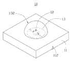
参见图1及图2,本发明第一实施例所提供的表面贴装型发光二极管组件10包括:基底11,发光二极管芯片12以及封装透镜13。Referring to FIG. 1 and FIG. 2 , the surface
该基底11用于承载所述发光二极管芯片12,其材质可为氮化镓等半导体材料。该基底11上还设置有用于向发光二极管芯片12供电的第一电极110、第二电极112,该第一电极110、第二电极112分别与发光二极管芯片12电连接并在基底11上形成焊盘结构。The
该发光二极管芯片12设置在基底11上,其可为氮化镓(GaN)发光二极管芯片、氮化铟镓(InGaN)发光二极管芯片或磷化铝铟镓(AlInGaP)发光二极管芯片等。The
该封装透镜13设置在基底11上,并覆盖所述发光二极管芯片12。该封装透镜13的材质可为树脂、玻璃或硅胶等透明材料。本实施例中,该封装透镜13的材质为树脂,如环氧树脂或聚甲基丙烯酸甲酯等。该封装透镜13包括出光面132,所述发光二极管芯片12发出的光线可到达出光面132并出射至封装透镜13外部。该出光面132为沿远离基底11的方向凸起的半圆球面,且该出光面132的球心与设置在基底11上的发光二极管芯片12基本重合,从而发光二极管芯片12发出的光线可经由封装透镜13内部以近似于0度入射角入射至出光面132的各个区域,进而最大限度的减少全反射现象的发生而具有较高的出光效率。The
可以理解的是,该出光面132并不局限于所述半圆球面,其也可为1/3圆球面,1/4圆球面或抛物面等。从而经由封装透镜13内部入射至出光面132的光线可具有尽量小的入射角,以减少全反射现象的发生,确保表面贴装型发光二极管组件10拥有尽可能高的出光效率。It can be understood that the light-emitting
由此可见,本实施例提供的表面贴装型发光二极管组件10,其出光面132沿一远离基底11的方向凸起而形成曲面,从而可使来自发光二极管芯片12的光线经由封装透镜13以尽可能小的入射角度入射至该出光面132,以减少在出光面132处的全反射现象的发生,其具有出光效率高的特点。It can be seen that, in the surface mount type light
参见图3,本发明第二实施例提供一种采用该种表面贴装型发光二极管组件10的背光模组20。该背光模组20包括表面贴装型发光二极管组件10以及导光板22。Referring to FIG. 3 , the second embodiment of the present invention provides a backlight module 20 using such a surface
该导光板22的材质可为塑胶、树脂、玻璃或硅胶等透明材料,其包括一第一表面220。该第一表面220上向内凹设有收容部222,所述表面贴装型发光二极管组件10设置在导光板22的第一表面220一侧,且该表面贴装型发光二极管组件10的封装透镜13收容在所述导光板22的收容部222内。The light guide plate 22 can be made of transparent materials such as plastic, resin, glass or silicone, and includes a first surface 220 . The first surface 220 is concavely provided with a receiving portion 222, the surface mount type light
该收容部222的内表面为曲面,用于接收表面贴装型发光二极管组件10发出的光线,并且该内表面的曲率半径大于或等于所述出光面132的曲率半径。优选的,该收容部222的内表面的曲率半径大于出光面132的曲率半径。该收容部222的内表面与封装透镜13的出光面132之间的间隙通过填充材料24填充。该填充材料24可以在稍微施加压力之下通过加温烘烤工艺而固化,从而将表面贴装型发光二极管组件10与导光板22固定。The inner surface of the accommodating portion 222 is a curved surface for receiving the light emitted by the surface mount
为保证填充材料24、封装透镜13以及导光板22的材质折射率无明显的差异,从而避免界面间的光干涉现象,该填充材料24的材质折射率优选为介于所述封装透镜13及导光板22的材质折射率之间。由于本实施例中封装透镜13以及导光板22的折射率位于1.4~1.5之间,故该填充材料24的材质的折射率优选为1.4~1.5之间。更优选的,所述填充材料24、封装透镜13以及导光板22三者的材质折射率均相同。In order to ensure that there is no significant difference in the material refractive index of the filling material 24, the
基于上述填充材料的折射率的考量,本实施例中选用硅胶作为填充材料24。另外,由于硅胶为质地柔软的透光材质,使用硅胶作为填充材料24可使封装透镜13与导光板22之间形成良好接触、无间隙的接合面,并且硅胶本身易于清除,更有利于后续的维修和重工工艺。当然,该填充材料24也可采用粘滞系数较高的液体,从而可使得背光模组的加工及维修工艺极为便利。所述填充材料24的材质可为胶体、凝胶、环氧树脂、玻璃或硅胶等,并且该填充材料24内还可掺杂有荧光粉,或该填充材料24表面形成有一荧光粉层。Based on the consideration of the above-mentioned refractive index of the filling material, silica gel is selected as the filling material 24 in this embodiment. In addition, since silica gel is a soft light-transmitting material, using silica gel as the filling material 24 can form a good contact and gap-free bonding surface between the
可以理解的是,所述表面贴装型发光二极管组件的封装透镜并不局限于如上所述的半圆球面、抛物面等规则的曲面。如图4及图5所示,本发明第三实施例还提供一种表面贴装型发光二极管组件30。该表面贴装型发光二极管组件30与表面贴装型发光二极管组件10的结构基本相同,其包括基底31以及设置在基底31上的发光二极管芯片32及封装透镜33,不同之处在于,该封装透镜33的出光面包括第一出光部3321、第二出光部3322以及第三出光部3323。该第三出光部3323分别与第一出光部3321、第二出光部3322相邻,且该第一出光部3321与第二出光部3322相对设置在第三出光部3323的两侧,所述第一出光部3321及第二出光部3322为曲率相同的两个曲面,所述第三出光部3323为曲率大于第一出光部3321及第二出光部3322的曲面。It can be understood that the encapsulation lens of the surface mount type light emitting diode assembly is not limited to regular curved surfaces such as hemispherical surface and paraboloid as mentioned above. As shown in FIG. 4 and FIG. 5 , the third embodiment of the present invention also provides a surface
由于第三出光部3323的曲率比第一出光部3321及第二出光部3322大,相较而言:入射至第三出光部3323上的与第一出光部3321或第二出光部3322相邻的区域的光线,其入射角相对较小而不容易发生全反射现象;入射至第一出光部3321或第二出光部3322上的与第三出光部3323相邻的区域的光线,其入射角相对较大而容易发生全反射现象。因此入射至第三出光部3323的光线出光效率较高,而入射至第一出光部3321及第二出光部3322的光线将因全反射而被导向第三出光部3323出射,以增强第三出光部3323的出光强度。Since the curvature of the third
从而,通过适当控制封装透镜33的各部分出光面曲率的大小,便可选择性地控制封装透镜33各个局部出光区域的出光强度,以满足背光模组20的各种光学需求。当然,所述第一出光部3321及第二出光部3322并不局限为曲率相同的两个曲面,该二者还可为曲率不同的两个曲面,或一者为曲面而另一者为平面,或二者均为平面等。Therefore, by properly controlling the curvature of each part of the light emitting surface of the encapsulating
另外,本领域技术人员还可在本发明精神内做其它变化,如适当变更封装透镜的形状,出光面的曲率半径,发光二极管芯片的种类以及导光板的类型等,只要其不偏离本发明的技术效果均可。这些依据本发明精神所做的变化,都应包含在本发明所要求保护的范围之内。In addition, those skilled in the art can also make other changes within the spirit of the present invention, such as appropriately changing the shape of the package lens, the radius of curvature of the light-emitting surface, the type of the light-emitting diode chip, and the type of the light guide plate, as long as it does not deviate from the spirit of the present invention. Technical effects are acceptable. These changes made according to the spirit of the present invention should be included in the scope of protection of the present invention.
Claims (4)
Translated fromChinesePriority Applications (2)
| Application Number | Priority Date | Filing Date | Title |
|---|---|---|---|
| CN2007102013580ACN101369619B (en) | 2007-08-14 | 2007-08-14 | Surface labeling type LED component and LED back light module unit |
| US12/013,920US7762692B2 (en) | 2007-08-14 | 2008-01-14 | Surface mount light emitting diode assembly and backlight module using the same |
Applications Claiming Priority (1)
| Application Number | Priority Date | Filing Date | Title |
|---|---|---|---|
| CN2007102013580ACN101369619B (en) | 2007-08-14 | 2007-08-14 | Surface labeling type LED component and LED back light module unit |
Publications (2)
| Publication Number | Publication Date |
|---|---|
| CN101369619A CN101369619A (en) | 2009-02-18 |
| CN101369619Btrue CN101369619B (en) | 2011-01-05 |
Family
ID=40362806
Family Applications (1)
| Application Number | Title | Priority Date | Filing Date |
|---|---|---|---|
| CN2007102013580AActiveCN101369619B (en) | 2007-08-14 | 2007-08-14 | Surface labeling type LED component and LED back light module unit |
Country Status (2)
| Country | Link |
|---|---|
| US (1) | US7762692B2 (en) |
| CN (1) | CN101369619B (en) |
Families Citing this family (44)
| Publication number | Priority date | Publication date | Assignee | Title |
|---|---|---|---|---|
| TWI397195B (en)* | 2008-07-07 | 2013-05-21 | Advanced Optoelectronic Tech | Light-emitting diode component and backlight module |
| JP2010092705A (en)* | 2008-10-08 | 2010-04-22 | Sony Corp | Illuminating device and display device using this |
| USD601281S1 (en)* | 2009-01-22 | 2009-09-29 | Mary Elle Fashions | LED night-light with square illuminator |
| USD612522S1 (en) | 2009-01-22 | 2010-03-23 | Mary Elle Fashions | LED night-light with truncated hemisphere |
| US8773616B2 (en) | 2009-10-19 | 2014-07-08 | Panasonic Corporation | Illuminating lens, lighting device, surface light source, and liquid crystal display apparatus |
| USD636741S1 (en)* | 2009-12-22 | 2011-04-26 | Panasonic Corporation | Light-emitting diode |
| USD636743S1 (en)* | 2009-12-22 | 2011-04-26 | Panasonic Corporation | Light-emitting diode |
| TWD144346S (en)* | 2009-12-22 | 2011-12-21 | 松下電器產業股份有限公司 | Light-emitting diode |
| USD636742S1 (en)* | 2009-12-22 | 2011-04-26 | Panasonic Corporation | Light-emitting diode |
| TW201123411A (en)* | 2009-12-30 | 2011-07-01 | Harvatek Corp | A light emission module with high-efficiency light emission and high-efficiency heat dissipation and applications thereof |
| TW201123412A (en)* | 2009-12-30 | 2011-07-01 | Harvatek Corp | A light emission module with high-efficiency light emission and high-efficiency heat dissipation and applications thereof |
| KR20110080318A (en)* | 2010-01-05 | 2011-07-13 | 엘지이노텍 주식회사 | Light emitting device package |
| USD650342S1 (en)* | 2010-06-22 | 2011-12-13 | Panasonic Corporation | Light emitting diode |
| USD642141S1 (en)* | 2010-06-22 | 2011-07-26 | Panasonic Corporation | Light emitting diode |
| USD650341S1 (en)* | 2010-06-22 | 2011-12-13 | Panasonic Corporation | Light emitting diode |
| USD645419S1 (en)* | 2010-06-22 | 2011-09-20 | Panasonic Corporation | Light emitting diode |
| USD646235S1 (en)* | 2010-06-22 | 2011-10-04 | Panasonic Corporation | Light emitting diode |
| USD645420S1 (en)* | 2010-06-22 | 2011-09-20 | Panasonic Corporation | Light emitting diode |
| USD649944S1 (en)* | 2010-07-07 | 2011-12-06 | Panasonic Corporation | Light emitting diode |
| USD649943S1 (en)* | 2010-07-07 | 2011-12-06 | Panasonic Corporation | Light emitting diode |
| USD642142S1 (en)* | 2010-07-07 | 2011-07-26 | Panasonic Corporation | Light emitting diode |
| USD642143S1 (en)* | 2010-07-07 | 2011-07-26 | Panasonic Corporation | Light emitting diode |
| US10147853B2 (en) | 2011-03-18 | 2018-12-04 | Cree, Inc. | Encapsulant with index matched thixotropic agent |
| KR20130022060A (en)* | 2011-08-24 | 2013-03-06 | 삼성디스플레이 주식회사 | Backlight assembly and method of manufacturing the same |
| KR101291141B1 (en)* | 2011-08-25 | 2013-08-01 | 삼성전자주식회사 | Backlight unit including light emitting device module of cob type |
| KR20130104628A (en)* | 2012-03-14 | 2013-09-25 | 서울반도체 주식회사 | Led illumination module |
| US9818919B2 (en) | 2012-06-11 | 2017-11-14 | Cree, Inc. | LED package with multiple element light source and encapsulant having planar surfaces |
| US10468565B2 (en) | 2012-06-11 | 2019-11-05 | Cree, Inc. | LED package with multiple element light source and encapsulant having curved and/or planar surfaces |
| US10424702B2 (en) | 2012-06-11 | 2019-09-24 | Cree, Inc. | Compact LED package with reflectivity layer |
| US9887327B2 (en) | 2012-06-11 | 2018-02-06 | Cree, Inc. | LED package with encapsulant having curved and planar surfaces |
| US9461024B2 (en) | 2013-08-01 | 2016-10-04 | Cree, Inc. | Light emitter devices and methods for light emitting diode (LED) chips |
| USD758976S1 (en) | 2013-08-08 | 2016-06-14 | Cree, Inc. | LED package |
| CN104141912A (en)* | 2014-08-21 | 2014-11-12 | 深圳市华星光电技术有限公司 | Curved surface shaped backlight module and curved surface shaped liquid crystal displayer |
| KR20160038568A (en)* | 2014-09-30 | 2016-04-07 | (주)포인트엔지니어링 | Chip substrate comprising plural curve surface cavity |
| USD790486S1 (en) | 2014-09-30 | 2017-06-27 | Cree, Inc. | LED package with truncated encapsulant |
| US11125412B2 (en)* | 2014-12-01 | 2021-09-21 | Current Lighting Solutions, Llc | Lighting device with efficient light-spreading lens system |
| USD777122S1 (en) | 2015-02-27 | 2017-01-24 | Cree, Inc. | LED package |
| USD783547S1 (en) | 2015-06-04 | 2017-04-11 | Cree, Inc. | LED package |
| KR102340515B1 (en)* | 2015-11-02 | 2021-12-16 | 엘지전자 주식회사 | Backlight unit and display apparatus comprising the same |
| TWI567329B (en)* | 2016-06-24 | 2017-01-21 | 東貝光電科技股份有限公司 | Primary optical illumination source with rectangular light pattern |
| CN112086550A (en)* | 2020-10-13 | 2020-12-15 | 扬州紫王优卫科技有限公司 | Quartz focusing lens with inner cavity for LED packaging |
| CN112614925A (en)* | 2020-12-24 | 2021-04-06 | 广东晶科电子股份有限公司 | Light-emitting device and module |
| KR20220149858A (en)* | 2021-04-30 | 2022-11-09 | 삼성디스플레이 주식회사 | Display device |
| CN114460779A (en)* | 2022-03-03 | 2022-05-10 | 深圳创维-Rgb电子有限公司 | LED lamp panel, backlight module, display device and preparation method of LED lamp panel |
Citations (1)
| Publication number | Priority date | Publication date | Assignee | Title |
|---|---|---|---|---|
| CN2646871Y (en)* | 2003-08-25 | 2004-10-06 | 上海芦三科技发展有限公司 | A LED with surface sticking structure and oval lens |
Family Cites Families (11)
| Publication number | Priority date | Publication date | Assignee | Title |
|---|---|---|---|---|
| JP3187280B2 (en)* | 1995-05-23 | 2001-07-11 | シャープ株式会社 | Surface lighting device |
| US6712481B2 (en)* | 1995-06-27 | 2004-03-30 | Solid State Opto Limited | Light emitting panel assemblies |
| US5959316A (en)* | 1998-09-01 | 1999-09-28 | Hewlett-Packard Company | Multiple encapsulation of phosphor-LED devices |
| US6547423B2 (en) | 2000-12-22 | 2003-04-15 | Koninklijke Phillips Electronics N.V. | LED collimation optics with improved performance and reduced size |
| CN1381904A (en) | 2001-04-18 | 2002-11-27 | 银河光电有限公司 | Package of LED chip and its light-gathering lens |
| US6676318B2 (en)* | 2001-10-26 | 2004-01-13 | Hewlett-Packard Development Company, L.P. | Printer media tray and method of using same |
| US7264378B2 (en)* | 2002-09-04 | 2007-09-04 | Cree, Inc. | Power surface mount light emitting die package |
| US7280288B2 (en)* | 2004-06-04 | 2007-10-09 | Cree, Inc. | Composite optical lens with an integrated reflector |
| TWI398188B (en)* | 2004-08-31 | 2013-06-01 | Showa Denko Kk | A luminous body, and a lighting and display device using the luminous body |
| EP2757401A1 (en)* | 2005-04-26 | 2014-07-23 | LG Innotek Co., Ltd. | Optical lens, light emitting device package using the optical lens, and backlight unit |
| CN1688029A (en) | 2005-05-09 | 2005-10-26 | 葛世潮 | High efficient LED |
- 2007
- 2007-08-14CNCN2007102013580Apatent/CN101369619B/enactiveActive
- 2008
- 2008-01-14USUS12/013,920patent/US7762692B2/enactiveActive
Patent Citations (1)
| Publication number | Priority date | Publication date | Assignee | Title |
|---|---|---|---|---|
| CN2646871Y (en)* | 2003-08-25 | 2004-10-06 | 上海芦三科技发展有限公司 | A LED with surface sticking structure and oval lens |
Also Published As
| Publication number | Publication date |
|---|---|
| US20090046470A1 (en) | 2009-02-19 |
| US7762692B2 (en) | 2010-07-27 |
| CN101369619A (en) | 2009-02-18 |
Similar Documents
| Publication | Publication Date | Title |
|---|---|---|
| CN101369619B (en) | Surface labeling type LED component and LED back light module unit | |
| JP6058351B2 (en) | LIGHT SOURCE MODULE AND LIGHTING DEVICE HAVING THE SAME | |
| KR100928635B1 (en) | Side Light Emitting Diode Package | |
| JP6442199B2 (en) | Light emitting device package | |
| CN102651442B (en) | LED light source | |
| CN101567366A (en) | Light emitting diode | |
| TWI566437B (en) | Light emitting device and method of manufacturing same | |
| US8476662B2 (en) | Light emitting device, method for manufacturing the same, and backlight unit | |
| US20130234183A1 (en) | Led module | |
| TWI479235B (en) | Edge type led backlight unit | |
| US20170069806A1 (en) | Light-emitting element package | |
| CN102185082B (en) | Light-emitting diode structure and light-emitting diode structure manufacturing method | |
| CN107919431B (en) | LED chip scale package structure and direct type backlight module | |
| KR101844477B1 (en) | A Light emitting device package | |
| KR102160775B1 (en) | A light emitting device package | |
| CN114267770B (en) | Backlight module and display device | |
| TWI352419B (en) | Light emitting unit | |
| CN103531583A (en) | Light emitting diode array module | |
| TWI427757B (en) | Light emitting diode package structure and related illuminate component and direct type emitting module and display device | |
| CN1937265A (en) | LED light source product | |
| US20140177275A1 (en) | Led backlight module having reduced light leakage and increased light extraction efficiency | |
| TW200913313A (en) | Surface mounted light emitting diode assembly and light emitting diode backlight module | |
| KR20150017594A (en) | Lighting apparatus | |
| KR102617482B1 (en) | Led package and direct type backlight unit comprising the same | |
| KR101675588B1 (en) | Light emitting device package |
Legal Events
| Date | Code | Title | Description |
|---|---|---|---|
| C06 | Publication | ||
| PB01 | Publication | ||
| C10 | Entry into substantive examination | ||
| SE01 | Entry into force of request for substantive examination | ||
| C14 | Grant of patent or utility model | ||
| GR01 | Patent grant | ||
| C56 | Change in the name or address of the patentee | ||
| CP01 | Change in the name or title of a patent holder | Address after:201600 Shanghai City, Songjiang District Songjiang Industrial Zone West science and Technology Industrial Park No. 500 Wen Ji Lu Patentee after:Foxsemicon Integrated Technology (Shanghai) Inc. Patentee after:Foxsemicon Integrated Technology Inc. Address before:201600 Shanghai City, Songjiang District Songjiang Industrial Zone West science and Technology Industrial Park No. 500 Wen Ji Lu Patentee before:Foxsemicon Integrated Technology (Shanghai) Inc. Patentee before:Foxsemicon Integrated Technology Inc. | |
| C41 | Transfer of patent application or patent right or utility model | ||
| C56 | Change in the name or address of the patentee | ||
| CP01 | Change in the name or title of a patent holder | Address after:201600 Shanghai City, Songjiang District Songjiang Industrial Zone West science and Technology Industrial Park No. 500 Wen Ji Lu Patentee after:Foxsemicon Integrated Technology (Shanghai) Inc. Patentee after:FOXSEMICON INTEGRATED TECHNOLOGY Inc. Address before:201600 Shanghai City, Songjiang District Songjiang Industrial Zone West science and Technology Industrial Park No. 500 Wen Ji Lu Patentee before:Foxsemicon Integrated Technology (Shanghai) Inc. Patentee before:Foxsemicon Integrated Technology Inc. | |
| TR01 | Transfer of patent right | Effective date of registration:20160225 Address after:Tokushima, Japan Patentee after:NICHIA Corp. Address before:American California Patentee before:Joint insurance trust company I Effective date of registration:20160225 Address after:American California Patentee after:Joint insurance trust company I Address before:201600 Shanghai City, Songjiang District Songjiang Industrial Zone West science and Technology Industrial Park No. 500 Wen Ji Lu Patentee before:Foxsemicon Integrated Technology (Shanghai) Inc. Patentee before:FOXSEMICON INTEGRATED TECHNOLOGY Inc. |