CN101366101A - Method and apparatus for igniting a low pressure plasma - Google Patents
Method and apparatus for igniting a low pressure plasmaDownload PDFInfo
- Publication number
- CN101366101A CN101366101ACNA2006800238282ACN200680023828ACN101366101ACN 101366101 ACN101366101 ACN 101366101ACN A2006800238282 ACNA2006800238282 ACN A2006800238282ACN 200680023828 ACN200680023828 ACN 200680023828ACN 101366101 ACN101366101 ACN 101366101A
- Authority
- CN
- China
- Prior art keywords
- plasma
- plasma processing
- electrode
- ignition electrode
- substrate
- Prior art date
- Legal status (The legal status is an assumption and is not a legal conclusion. Google has not performed a legal analysis and makes no representation as to the accuracy of the status listed.)
- Granted
Links
Images


Classifications
- H—ELECTRICITY
- H01—ELECTRIC ELEMENTS
- H01L—SEMICONDUCTOR DEVICES NOT COVERED BY CLASS H10
- H01L21/00—Processes or apparatus adapted for the manufacture or treatment of semiconductor or solid state devices or of parts thereof
- H01L21/02—Manufacture or treatment of semiconductor devices or of parts thereof
- H01L21/04—Manufacture or treatment of semiconductor devices or of parts thereof the devices having potential barriers, e.g. a PN junction, depletion layer or carrier concentration layer
- H01L21/18—Manufacture or treatment of semiconductor devices or of parts thereof the devices having potential barriers, e.g. a PN junction, depletion layer or carrier concentration layer the devices having semiconductor bodies comprising elements of Group IV of the Periodic Table or AIIIBV compounds with or without impurities, e.g. doping materials
- H01L21/30—Treatment of semiconductor bodies using processes or apparatus not provided for in groups H01L21/20 - H01L21/26
- H01L21/302—Treatment of semiconductor bodies using processes or apparatus not provided for in groups H01L21/20 - H01L21/26 to change their surface-physical characteristics or shape, e.g. etching, polishing, cutting
- H—ELECTRICITY
- H01—ELECTRIC ELEMENTS
- H01J—ELECTRIC DISCHARGE TUBES OR DISCHARGE LAMPS
- H01J37/00—Discharge tubes with provision for introducing objects or material to be exposed to the discharge, e.g. for the purpose of examination or processing thereof
- H01J37/32—Gas-filled discharge tubes
- H01J37/32009—Arrangements for generation of plasma specially adapted for examination or treatment of objects, e.g. plasma sources
- H01J37/32082—Radio frequency generated discharge
- H01J37/321—Radio frequency generated discharge the radio frequency energy being inductively coupled to the plasma
Landscapes
- Engineering & Computer Science (AREA)
- Physics & Mathematics (AREA)
- Plasma & Fusion (AREA)
- Chemical & Material Sciences (AREA)
- Analytical Chemistry (AREA)
- General Physics & Mathematics (AREA)
- Condensed Matter Physics & Semiconductors (AREA)
- Manufacturing & Machinery (AREA)
- Computer Hardware Design (AREA)
- Microelectronics & Electronic Packaging (AREA)
- Power Engineering (AREA)
- Drying Of Semiconductors (AREA)
- Plasma Technology (AREA)
Abstract
Description
Translated fromChinese技术领域technical field
本发明总体上涉及基片制造技术,尤其涉及用于引燃(igniting)低压等离子体的方法和装置。The present invention relates generally to substrate fabrication techniques, and more particularly to methods and apparatus for igniting low-pressure plasmas.
背景技术Background technique
在基片(例如,半导体晶片,MEMS器件或如在平板显示器制造中使用的玻璃平板)的处理过程中,通常使用等离子体。作为基片处理(化学气相沉积,等离子体增强化学气相沉积,物理气相沉积,蚀刻等)的一部分,例如,该基片被分为多个模片,或者矩形区域,其中每个将变为一个集成电路。然后该基片在一系列步骤中被处理,其中有选择地去除(蚀刻)和沉积(沉积)材料以在其上形成电气元件。Plasmas are commonly used during the processing of substrates such as semiconductor wafers, MEMS devices or glass panels such as are used in the manufacture of flat panel displays. As part of substrate processing (chemical vapor deposition, plasma enhanced chemical vapor deposition, physical vapor deposition, etching, etc.), for example, the substrate is divided into dies, or rectangular regions, each of which becomes a integrated circuit. The substrate is then processed in a series of steps in which material is selectively removed (etched) and deposited (deposited) to form electrical components thereon.
随着器件尺寸缩减以及使用更先进的材料,为保持均一的蚀刻率,减小基片污染等,对充分稳定的处理条件的要求变得更加迫切。这将被对基片上高电路密度的逐步上升的要求进一步加重,使用现有的等离子体处理技术会很难满足,在该技术中亚微米过孔接触和沟槽具有高纵横比。As device dimensions shrink and more advanced materials are used, the need for sufficiently stable processing conditions to maintain uniform etch rates, reduce substrate contamination, etc. becomes more urgent. This will be further exacerbated by the escalating demand for high circuit density on substrates, which would be difficult to meet using existing plasma processing techniques in which sub-micron via contacts and trenches have high aspect ratios.
通常,有三种蚀刻方法:纯化学蚀刻,纯物理蚀刻,以及反应性离子蚀刻。纯化学蚀刻通常不包括物理轰击,而是与基片上的材料发生化学反应。纯离子蚀刻,经常称为溅射,通常使用等离子体离子化的惰性气体,如氩,以从该基片移走材料。结合化学和离子两种方法的蚀刻被经常称为反应性离子蚀刻(RIE),或离子辅助蚀刻。Generally, there are three etching methods: pure chemical etching, pure physical etching, and reactive ion etching. Purely chemical etching usually does not involve physical bombardment, but rather a chemical reaction with the material on the substrate. Pure ion etching, often called sputtering, typically uses a plasma ionized inert gas, such as argon, to remove material from the substrate. Etching that combines both chemical and ionic methods is often referred to as reactive ion etching (RIE), or ion-assisted etching.
在这些和其他类型的等离子体方法中,在许多等离子体处理方法中经常要求的压力范围内很难引燃等离子体。通常,当RF功率施加在一组电极上时,在它们之间建立变化的电场。如果该RF功率足够高,自由电子可由该变化的电场加速,直到其获得足够的能量以碰撞该室内的原子或分子,以产生离子或另一个自由电子。因为该离子化碰撞的级联作用,整个等离子体室迅速充满电子和离子(如,等离子体)。在等离子体中,一些电子由与电极、等离子体室壁的碰撞所持续损失和消耗,并且还由电子和离子之间的碰撞重新组合、以及被中性物质附着所持续损失和消耗。因此,等离子体室的电离速率主要由电子能量确定,而该电子能量又由所施加的功率控制。In these and other types of plasma processes, it is difficult to ignite the plasma in the pressure ranges often required in many plasma processing methods. Typically, when RF power is applied across a set of electrodes, a varying electric field is established between them. If the RF power is high enough, free electrons can be accelerated by the changing electric field until they gain enough energy to collide with atoms or molecules within the chamber to produce an ion or another free electron. Because of this cascade of ionizing collisions, the entire plasma chamber is rapidly filled with electrons and ions (eg, plasma). In a plasma, some electrons are continuously lost and consumed by collisions with electrodes, plasma chamber walls, and also by recombination by collisions between electrons and ions, and by attachment of neutral species. Thus, the ionization rate of the plasma chamber is primarily determined by the electron energy, which in turn is controlled by the applied power.
取决于许多额外的因素,包括等离子体气体化学性质、电极材料、等离子体室尺寸、RF传送方法(例如,电感耦合,电容耦合等)、电激发频率等,引燃和维持等离子体会有困难,如果该气体压力相对低(如,电容放电中<100mT等)。即,低于临界激发压力,等离子体不能被自维持(self-sustained)地引燃,因为由离子化碰撞导致的电子的生成率会低于电子的损失率。甚至这样的情形下也是如此,即预先建立的等离子体可转变为低于该临界激发压力的压力,而没有等离子体熄灭。Depending on many additional factors, including plasma gas chemistry, electrode materials, plasma chamber dimensions, RF delivery method (e.g., inductive coupling, capacitive coupling, etc.), electrical excitation frequency, etc., it can be difficult to ignite and maintain a plasma, If the gas pressure is relatively low (eg <100mT in capacitor discharge, etc.). That is, below the critical excitation pressure, the plasma cannot be self-sustained to ignite because the rate of electron generation by ionizing collisions will be lower than the rate of electron loss. This is even the case where a pre-established plasma can be transitioned to a pressure below the critical excitation pressure without extinction of the plasma.
一种解决方案可以通过临时增加气体压力来维持等离子体,这从而也增加等离子体气体密度以及由此的与原子或分子的碰撞次数。即,将电子的生成率增加到高于电子的损失率。一旦该等离子体被引燃并稳定在较高压力,该等离子体室被转变到较低的目标压力,以处理该基片。目标是指在该等离子体处理方法中的可接受的数值范围(例如,目标压力、目标功率、目标气体流量等)。然而,将基片暴露于更高压等离子体(非稳定状态条件),即使是瞬时的,也可能在特定的基片上引入不需要的结果,或者引入基片之间不能接受的质量波动。One solution could be to maintain the plasma by temporarily increasing the gas pressure, which in turn also increases the plasma gas density and thus the number of collisions with atoms or molecules. That is, the generation rate of electrons is increased to be higher than the loss rate of electrons. Once the plasma is ignited and stabilized at the higher pressure, the plasma chamber is transitioned to a lower target pressure to process the substrate. A target refers to an acceptable numerical range (eg, target pressure, target power, target gas flow, etc.) in the plasma processing method. However, exposing substrates to higher pressure plasmas (non-steady state conditions), even momentarily, may introduce unwanted results on specific substrates, or unacceptable quality fluctuations between substrates.
另一个解决方案可在较高频率下操作该等离子体室。通常,与由较低频率的信号以类似的功率水平激发(excite)相比,由于更有效的电子加热机制,较高频率易于更有效地产生等离子体密度。然而,增加等离子体处理频率也是有问题的。例如,由于电磁驻波和趋肤效应,较高的频率可导致较差的均一性(M.A.Lieberman等人,Standing wave and skin effects in large-area,high frequency capacitivedischarges,Plasma Sources Sci.Technol.11(2002)283-293)。其他的问题可能包括导致因为调整的电子温度而发生的等离子体化学性质和离子/自由基比率的改变,以及由于增加的灵敏度而很难匹配工具对工具的性能以偏离在该RF传送和接地返回系统中的电容和电感。Another solution could be to operate the plasma chamber at a higher frequency. In general, higher frequencies tend to generate plasma densities more efficiently than excited by lower frequency signals at similar power levels due to more efficient electron heating mechanisms. However, increasing the frequency of plasma processing is also problematic. For example, higher frequencies can lead to poorer uniformity due to electromagnetic standing waves and skin effects (M.A. Lieberman et al., Standing wave and skin effects in large-area, high frequency capacitive discharges, Plasma Sources Sci. Technol. 11( 2002) 283-293). Other issues may include changes in plasma chemistry and ion/radical ratios due to tuned electron temperature, and difficulty matching tool-to-tool performance due to increased sensitivity to deviations in the RF transmit and ground return Capacitance and inductance in the system.
另一解决方案可在短激发步骤中将更高的压力与被优化用于引燃等离子体的不同的气体流率结合,之后,该等离子体室转变为较低的运行目标压力和合适的目标气体流率以处理该基片。然而,如前所述,大体上从该工艺方法的偏离会引入在特定的基片上的不需要的结果,或基片之间不能接受的质量波动。Another solution could be to combine a higher pressure with a different gas flow rate optimized to ignite the plasma in a short excitation step, after which the plasma chamber transitions to a lower operating target pressure and a suitable target gas flow rate to process the substrate. However, as previously stated, generally deviations from the process method can introduce unwanted results on a particular substrate, or unacceptable quality fluctuations between substrates.
又一个熟知的减小窄隙电容放电系统中临界激发压力的方法是增加电极间隙。通常,平均自由程(mean free path)定义为一个粒子在与另一个粒子碰撞之前行进的平均距离。随后,增加该电极间隙也可增加该平均自由程,通过增加该等离子体室的电离速率而稳定低压等离子体(例如,<100mT等)。然而,增加该间隙尺寸也会有问题。例如,较大的间隙会由于较低的功率密度而降低蚀刻率,会由于较长的气体停留时间而增加室条件记忆效应,以及当使用分区的气体引入时降低处理均一性。Yet another well-known method of reducing the critical excitation pressure in narrow-gap capacitive discharge systems is to increase the electrode gap. In general, the mean free path is defined as the average distance a particle travels before colliding with another particle. Subsequently, increasing the electrode gap can also increase the mean free path, stabilizing low pressure plasmas (eg, <100 mT, etc.) by increasing the ionization rate of the plasma chamber. However, increasing this gap size can also be problematic. For example, larger gaps reduce etch rates due to lower power densities, increase chamber condition memory effects due to longer gas residence times, and reduce process uniformity when zoned gas introduction is used.
例如,介电蚀刻反应器经常使用电容耦合RF激发源和相对窄的电极至电极间隙间距的组合。例如,与20至30cm基片尺寸相比,Lam Research ExelanTM族通常使用1.3至2.5cm间隙。这个电容耦合与窄隙的组合易于导致相当高的临界激发压力,其往往超过所需的处理压力。For example, dielectric etch reactors often use a combination of capacitively coupled RF excitation sources and relatively narrow electrode-to-electrode gap spacing. For example, the Lam Research Exelan™ family typically uses a 1.3 to 2.5 cm gap compared to a 20 to 30 cm substrate size. This combination of capacitive coupling and narrow gap tends to lead to rather high critical excitation pressures, which often exceed the required processing pressures.
现在参考图1,显示出电感耦合等离子体处理系统的简化图。通常,在特定的压力下,并以特定的方法混合的适合的气体组可从气体分配系统122流入具有等离子体室壁117的等离子体室102。这些等离子体处理气体可随后以特定RF功率设置组在靠近喷射器109的区域上或之内被离子化,以形成等离子体110,以便处理(例如,蚀刻或沉积)该基片114(如半导体基片或玻璃平板)的暴露区域,基片114利用边缘环115安置在静电卡盘116上。Referring now to FIG. 1 , a simplified diagram of an inductively coupled plasma processing system is shown. Generally, a suitable set of gases mixed in a particular way may flow from
第一RF发生器134生成该等离子体,并且控制该等离子体密度,而第二RF发生器138生成偏置RF,通常用于控制该DC偏置和离子轰击能量。进一步连接到源RF发生器134的是匹配网络136a,并连接到偏置RF发生器138的是匹配网络136b,其试图将该RF功率源的阻抗与等离子体110的阻抗匹配。此外,真空系统113,包括阀门112和一组泵111,通常用来从等离子体室102排出周围空气,以实现维持等离子体110和/或去除处理副产物所需要的压力。A
现在参考图2,显示出电容耦合等离子体处理系统的简化图。通常电容耦合等离子体处理系统可配置为具有单一的或多个独立的RF功率源。由源RF发生器234产生的源RF通常用于通过电容耦合生成该等离子体,以及控制该等离子体密度。由偏置RF发生器238生成的偏置RF,通常用以控制DC偏置和离子轰击能量。进一步连接到该源RF发生器234和偏置RF发生器238的是匹配网络236,其试图将该RF功率源的阻抗与等离子体220的阻抗进行匹配。其他形式的电容反应器具有连接到顶部电极204的RF功率源和匹配网络。另外,还有遵循类似的RF和电极布置的多阳极系统,如三极管。Referring now to FIG. 2, a simplified diagram of a capacitively coupled plasma processing system is shown. Typically capacitively coupled plasma processing systems can be configured with a single or multiple independent RF power sources. Source RF generated by
通常,在特定的压力和以特定的方式混合的适合的气体组穿过顶部电极204中的入口从气体分配系统222流入具有等离子体室壁217的等离子体室202。这些等离子体处理气体可随后以特定的RF功率设置组被离子化以形成等离子体220,以便处理(例如,蚀刻或沉积)基片214(如半导体晶片或玻璃平板)暴露的区域,基片214利用边缘环215安置在也作为电极的静电卡盘216上。此外,真空系统213,包括阀门212和一组泵211,通常用于从等离子体室202排出周围空气,以便实现保持等离子体220所要求的压力。Typically, a suitable set of gases mixed in a specific manner at a specific pressure flows from the
考虑到前述的,需要用于引燃低压等离子体的方法和装置。In view of the foregoing, there is a need for methods and apparatus for igniting low pressure plasmas.
发明内容Contents of the invention
在一个实施例中,本发明涉及在等离子体处理系统中用于引燃等离子体的方法,该系统具有等离子体处理室、至少一个通电的电极和一个引燃电极。该方法包括在该等离子体处理室内引入基片。该方法还包括将气体混合物流入该等离子体处理室;以激发(strike)频率激励(energize)该引燃电极;以及使用该引燃电极从该气体混合物激发等离子体。该方法进一步包括使用目标频率激励该至少一个通电的电极,其中该激发频率大于该目标频率;并且当在该等离子体处理室中处理该基片时去激励该引燃电极。In one embodiment, the invention relates to a method for igniting a plasma in a plasma processing system having a plasma processing chamber, at least one energized electrode, and an ignition electrode. The method includes introducing a substrate within the plasma processing chamber. The method also includes flowing a gas mixture into the plasma processing chamber; energizing the ignition electrode at a strike frequency; and striking a plasma from the gas mixture using the ignition electrode. The method further includes energizing the at least one energized electrode with a target frequency, wherein the energization frequency is greater than the target frequency; and de-energizing the ignition electrode while processing the substrate in the plasma processing chamber.
在另一个实施例中,本发明涉及等离子体引燃装置,该装置配置为在等离子体处理室中激发等离子体。该装置包括引燃电极,该引燃电极配置为以激发频率从气体混合物激发等离子体。该装置也包括至少一个通电的电极,该通电的电极配置为以目标频率维持该等离子体,其中该激发频率比目标频率高,该引燃电极的第一表面积大体上低于该至少一个通电电极的第二表面积,并且当在该等离子体处理室中处理基片时去激励该引燃电极。In another embodiment, the present invention is directed to a plasma ignition device configured to ignite a plasma in a plasma processing chamber. The apparatus includes an ignition electrode configured to excite a plasma from a gas mixture at an excitation frequency. The apparatus also includes at least one energized electrode configured to maintain the plasma at a target frequency, wherein the excitation frequency is higher than the target frequency, the ignition electrode having a first surface area substantially lower than the at least one energized electrode and de-energize the ignition electrode when processing a substrate in the plasma processing chamber.
在另一个实施例中,本发明涉及一种等离子体处理系统中用于引燃等离子体的装置,该系统具有等离子体处理室、至少一个通电的电极和一个引燃电极。该装置包括用于将基片引入该等离子体处理室的装置。该装置还包括用于将气体混合物流入该等离子体处理室的装置;用于以激发频率激励该引燃电极的装置;以及用于使用该引燃电极从该气体混合物激发等离子体的装置。该装置进一步包括用于使用目标频率激励该至少一个通电电极的装置,其中该激发频率高于该目标频率;以及用于当在该等离子体处理室中处理该基片时去激励该引燃电极的装置。In another embodiment, the invention relates to an apparatus for igniting a plasma in a plasma processing system having a plasma processing chamber, at least one energized electrode, and an ignition electrode. The apparatus includes means for introducing a substrate into the plasma processing chamber. The apparatus also includes means for flowing a gas mixture into the plasma processing chamber; means for exciting the ignition electrode at an excitation frequency; and means for exciting a plasma from the gas mixture using the ignition electrode. The apparatus further comprises means for energizing the at least one energized electrode with a target frequency, wherein the excitation frequency is higher than the target frequency; and for de-energizing the ignition electrode while processing the substrate in the plasma processing chamber installation.
本发明这些和其它特征将在下面的详细描述中结合附图详细描述。These and other features of the invention will be described in detail in the following detailed description when taken in conjunction with the accompanying drawings.
附图说明Description of drawings
在附图中,通过实例而不是限定示出本发明,并且其中相同的标号代表相同的元件,并且其中:In the accompanying drawings, the invention is shown by way of example and not limitation, and wherein like numerals represent like elements, and wherein:
图1示出了电感耦合的等离子体处理系统的简化图;Figure 1 shows a simplified diagram of an inductively coupled plasma processing system;
图2示出了电容耦合的等离子体处理系统的简化图;Figure 2 shows a simplified diagram of a capacitively coupled plasma processing system;
图3A-C说示出了根据本发明一个实施例,带有引燃电极的电容耦合的等离子体处理系统的简化图组;3A-C illustrate a simplified set of diagrams of a capacitively coupled plasma processing system with an ignition electrode according to one embodiment of the present invention;
图4示出根据本发明一个实施例,图3A-C所示的引燃电极的简化图;Figure 4 shows a simplified diagram of the ignition electrode shown in Figures 3A-C, according to one embodiment of the present invention;
图5示出根据本发明的一个实施例,对于不同的RF频率对比电子温度与电子随机加热功率的简化图;Figure 5 shows a simplified graph of electron temperature versus electron stochastic heating power for different RF frequencies, according to one embodiment of the present invention;
图6示出根据本发明一个实施例的用于在RF等离子体中氩和氦放电的击穿的帕邢(Paschen)曲线组的简化图表;6 shows a simplified diagram of the Paschen set of curves for the breakdown of argon and helium discharges in RF plasmas according to one embodiment of the invention;
图7示出根据本发明的一个实施例,击穿RF功率对固定间隙的压力的依赖的简化图;Figure 7 shows a simplified graph of the dependence of breakdown RF power on the pressure of a fixed gap according to one embodiment of the present invention;
图8示出根据本发明一个实施例,一组简化的用于引燃等离子体的步骤。Figure 8 illustrates a simplified set of steps for igniting a plasma, according to one embodiment of the present invention.
具体实施方式Detailed ways
现在将关于附图中所说明的一些优选实施例详细描述本发明。在下面描述中,说明许多具体的细节以便提供对本发明的彻底理解。然而,对于本领域的技术人员来说,显然,本发明可以不使用这些具体细节中的一些或全部而实现。在其他的例子中,公知的处理步骤和/或结构并没有详细描述,以避免不必要地混淆本发明。The invention will now be described in detail with respect to some preferred embodiments illustrated in the accompanying drawings. In the following description, numerous specific details are set forth in order to provide a thorough understanding of the present invention. It will be apparent, however, to one skilled in the art, that the present invention may be practiced without some or all of these specific details. In other instances, well known process steps and/or structures have not been described in detail to avoid unnecessarily obscuring the present invention.
尽管不希望受到理论的束缚,但此处,发明人相信,低压等离子体可由以一定频率(激发频率)传送引燃RF电压来引燃,该频率可高于运行频率(目标频率)组,其通常用于在处理过程中维持该低压等离子体压力。在一个实施例中,该引燃RF电压通过至少一个专门的电极(引燃电极)传送。在一个实施例中,该引燃电极与激发RF发生器相连接。在一个实施例中,与RF发生器组分开的RF发生器用来生成该目标频率。在一个实施例中,一旦引燃等离子体,其由等离子体室电极以低于或不同于该激发频率的目标频率组保持。在一个实施例中,一旦引燃等离子体,该引燃电极就去激励(de-energized)。在一个实施例中,该等离子体在目标压力下引燃以使稳定时间最小。在一个实施例中,利用目标气体流混合物引燃该等离子体以使稳定时间最小。在一个实施例中,该等离子体在目标功率下引燃以使稳定时间最小。While not wishing to be bound by theory, the inventors herein believe that a low pressure plasma may be ignited by delivering an ignition RF voltage at a frequency (excitation frequency) that may be higher than the operating frequency (target frequency) set, which Typically used to maintain this low pressure plasma pressure during processing. In one embodiment, the ignition RF voltage is delivered through at least one dedicated electrode (ignition electrode). In one embodiment, the ignition electrode is connected to an excitation RF generator. In one embodiment, an RF generator separate from the set of RF generators is used to generate the target frequency. In one embodiment, once the plasma is ignited, it is maintained by the plasma chamber electrodes at a target set of frequencies below or different from the excitation frequency. In one embodiment, the ignition electrode is de-energized once the plasma is ignited. In one embodiment, the plasma is ignited at a target pressure to minimize stabilization time. In one embodiment, the plasma is ignited using a target gas flow mixture to minimize settling time. In one embodiment, the plasma is ignited at a target power to minimize stabilization time.
与现有技术不同,本发明不需要增加电极间隙,因为通常不要求改变间隙。一般而言,增加顶部和底部电极之间的间隙也会增加等离子体容积,其会进而消极影响该等离子体处理结果。例如,消极影响可包括由于较低的功率密度而减小的蚀刻率,由于较长气体停留时间而增加的等离子体室条件记忆效应,以及当使用分区的气体引入时对处理均一性不够有效的控制。Unlike the prior art, the present invention does not require an increase in the electrode gap, as gap changes are generally not required. In general, increasing the gap between the top and bottom electrodes also increases the plasma volume, which in turn negatively affects the plasma processing results. For example, negative effects can include reduced etch rates due to lower power densities, increased plasma chamber condition memory effects due to longer gas residence times, and less effective effects on process uniformity when zoned gas introduction is used. control.
通常,在等离子体处理室中,当在电极之间间隙中的电子获得离子化气体分子所需的能量时,RF放电会引燃等离子体。随后,为了引燃放电,每个电子应当在损失于电极或室壁之前执行3-10次与气体分子的离子化碰撞(V.A.Lisovsky和V.D.Yegorenkov,Rfbreakdown of low-pressure gas and a novel method for determinationof electron-drift velocities in gases,J.Phys.D:Appl.Phys.31(19998)3349-3357)。在RF放电中,电子振动通常表现为在RF场中电子位移的幅度。这个幅度可与该放电驱动频率成反比并且必须可与用于有效RF击穿的电极间距相当或者较小。因此,对于给定的等离子体室条件组(固定的气体压力电极间距,电极材料,RF电压等),对于气体击穿,较高的RF频率通常比较低的RF频率更有效。Typically, in a plasma processing chamber, an RF discharge ignites the plasma when electrons in the gap between electrodes gain the energy needed to ionize gas molecules. Subsequently, to ignite the discharge, each electron should perform 3-10 ionizing collisions with gas molecules before being lost to electrodes or chamber walls (V.A. Lisovsky and V.D. Yegorenkov, Rfbreakdown of low-pressure gas and a novel method for determination of Electron-drift velocities in gases, J. Phys. D: Appl. Phys. 31(19998) 3349-3357). In RF discharges, electronic vibrations are usually manifested as the magnitude of electron displacement in the RF field. This magnitude can be inversely proportional to the discharge drive frequency and must be comparable to or smaller than the electrode spacing for effective RF breakdown. Therefore, for a given set of plasma chamber conditions (fixed gas pressure electrode spacing, electrode material, RF voltage, etc.), higher RF frequencies are generally more effective than lower RF frequencies for gas breakdown.
在一个实施例中,具有比顶部和底部电极表面积小的表面积的电极可用作引燃电极,以使在该基片上的有害影响最小,这些有害影响可包括在引燃电压去除之前,对稳定状态处理条件的初始部分的扰动。在实施例中,该引燃电极还可包括等离子体电探针。In one embodiment, electrodes having a smaller surface area than the top and bottom electrodes may be used as ignition electrodes to minimize detrimental effects on the substrate, which may include detrimental effects on stability before the ignition voltage is removed. A perturbation of the initial part of the state processing condition. In an embodiment, the ignition electrode may also include a plasma electrical probe.
例如,在Lam Research ExelanTM上使用施加在该基片电极上的RF的测量已经表明该临界激发压力的频率依从关系。对于O2灰化等离子体,该临界激发压力在28MHz为55mT,而在63MHz为3-5mT。对于典型的聚合过孔或沟槽条件,该临界激发压力在28MHz为23mT,而在63MHz为10mT。For example, measurements on a Lam Research Exelan™ using RF applied to the substrate electrode have shown a frequency dependence of the critical excitation pressure. ForO2 ashing plasmas, this critical excitation pressure is 55 mT at 28 MHz and 3-5 mT at 63 MHz. For typical polymeric via or trench conditions, the critical excitation pressure is 23 mT at 28 MHz and 10 mT at 63 MHz.
在一个实施例中,引燃电极可独立于该等离子体处理系统的主RF系统,从而简化实施。也就是说,将引燃电极集成在该底部或顶部电极会有问题,因为该主RF系统的高功率要求和准确的再现性标准通常会使集成昂贵、复杂。另外,集成的引燃电极的存在会对该等离子体处理产生不利影响,该处理可能会对杂散阻抗(strayimpedance)的微小变化敏感。随后,为了引燃的目的而增加到这个主RF系统的引燃子系统会使随着时间以及在等离子体处理系统之间一致性地精确控制RF的任务复杂化,而该任务已经非常困难并且非常昂贵。In one embodiment, the ignition electrode can be independent of the main RF system of the plasma processing system, thereby simplifying implementation. That said, integrating the ignition electrode on the bottom or top electrode can be problematic because the high power requirements and exact reproducibility criteria of the main RF system generally make integration expensive and complex. Additionally, the presence of an integrated ignition electrode can adversely affect the plasma process, which can be sensitive to small changes in stray impedance. Subsequently, the addition of an ignition subsystem to this main RF system for ignition purposes complicates the already difficult and very expensive.
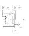
参考图3A-C,示出简化的图组,其示出了根据本发明一个实施例的简化的带有引燃电极的电容耦合的等离子体处理系统。图3A示出在等离子体引燃前的等离子体室。底部电极316通常地连接低频RF发生器338,而顶部电极304接地。另外,引燃电极305安装在该顶部电极304上,并且可由高频RF发生器334供电。Referring to Figures 3A-C, there is shown a simplified set of diagrams illustrating a simplified capacitively coupled plasma processing system with an ignition electrode in accordance with one embodiment of the present invention. Figure 3A shows the plasma chamber prior to plasma ignition. The
图3B示出已经引燃等离子体的图3A的等离子体室。在一个实施例中,当引燃等离子体时,低频RF发生器338在底部电极316和顶部电极304之间施加电压VLF。图3C示出图3B中的等离子体室,其中,引燃电极305已经被去激励(de-energized)并且等离子体310已经在等离子体室内基本稳定。Figure 3B shows the plasma chamber of Figure 3A after the plasma has been ignited. In one embodiment, the low
在一个实施例中,该引燃电极可与V/I探针相结合。通常,V/I可测量电压(V)、电流(I)、等离子体电压(V)和电流(I)之间的相位角(θ)、阻抗(Z)、输出功率、正向功率、反射功率、无功功率、反射系数等。即,一旦引燃等离子体并且该引燃电极被去激励(de-energized),其仍可用来测量等离子体处理条件。In one embodiment, the ignition electrode can be combined with a V/I probe. Typically, V/I measures voltage (V), current (I), phase angle (θ) between plasma voltage (V) and current (I), impedance (Z), output power, forward power, reflection Power, reactive power, reflection coefficient, etc. That is, once the plasma is ignited and the ignition electrode is de-energized, it can still be used to measure plasma processing conditions.
参考图4,示出根据本发明的一个实施例的如图3A-C所示的引燃电极305的简化图。如前所述,引燃电极305可安装在该顶部电极304中,并可由高频RF发生器334供电。另外,引燃电极305也可通过绝缘体404(如,陶瓷、石英等)与顶部电极304电绝缘。Referring to FIG. 4 , a simplified diagram of the
现在参考图5,根据本发明的一个实施例,对比不同RF频率下的电子温度与电子随机加热功率(electro stochastic heating power)的简化图表。电子温度502在水平轴上示出,而每单位面积的电子随机加热功率(W/M2)504在垂直轴上示出。通常,在RF放电中,施加的RF功率大部分通过电子与移动等离子体鞘(例如,随即加热)相互作用而转移到电子。用于单一的碰撞鞘的电子随机加热可建立为:Referring now to FIG. 5 , a simplified graph comparing electron temperature versus electron stochastic heating power at various RF frequencies is shown in accordance with one embodiment of the present invention.
其中,m是电子质量,e是元电荷,ε0是真空介电常数,ω是RF驱动频率,Te是电子温度,以及V1是穿过一个鞘的RF驱动电压(Lieberman M.A.和Lichtenberg A.J.1994 Principles of PlasmaDischarges and Materials Processing,New York:Wiley)。图5大体上示出使用方程1估算的电子随机加热对驱动频率依赖关系,其中固定电压V1=500伏特。通常,由于较高的频率在电子加热处理中更有效,激发和维持等离子体要求较小的电压V1。例如,在100MHz,随着该电子温度从1增加到10Te,产生的相应的随机加热功率从大约2.5×10³W/M2增加至大约8×103W/M2。相反,较低的频率通常在电子加热处理中是低效的。因此,激发和维持等离子体要求较大的电压V1。例如,在1MHz,随着电子温度从1增加到10Te,产生的相应的随机加热功率从大约0.0W/M2至大约0.6×103W/M2。where m is the electron mass, e is the elementary charge,ε0 is the vacuum permittivity, ω is the RF drive frequency,Te is the electron temperature, andV1 is the RF drive voltage across a sheath (Lieberman MA and Lichtenberg AJ1994 Principles of Plasma Discharges and Materials Processing, New York: Wiley). Figure 5 generally shows the dependence of stochastic heating of electrons on drive frequency estimated using
现在参考图6,示出用于氩和氦在RF等离子体中放电的击穿的帕邢曲线(Paschen curve)组的简化图表。Moravej等人,Physicsof high-pressure helium and argon radio-frequency plasmas,Journal ofApplied Physics,卷96,N12,pp.7011-7017。在水平轴上示出中性气体压力和电极间隙的乘积,pd(Torr-cm)602,而在该垂直轴上示出击穿电压(V)604。一般而言,击穿该放电所要求的电压是该中性气体压力和电极间隙的乘积pd的强函数(strong function)。Referring now to FIG. 6 , there is shown a simplified diagram of the set of Paschen curves for the breakdown of argon and helium discharges in RF plasmas. Moravej et al., Physics of high-pressure helium and argon radio-frequency plasmas, Journal of Applied Physics, Vol. 96, N12, pp. 7011-7017. The product of neutral gas pressure and electrode gap, pd (Torr-cm) 602 is shown on the horizontal axis, while breakdown voltage (V) 604 is shown on the vertical axis. In general, the voltage required to break down the discharge is a strong function of the product pd of the neutral gas pressure and the electrode gap.
氩等离子体曲线606和氦等离子体曲线608通过将压力在1至760Torr变化并使用三个不同间隙间距0.4、1.6和2.4mm而获得。氦等离子体606通常在大约4Torr-cm的pd表现出最小的击穿电压,而氩的最小值通常是不确定的。比较起来,在通过使用铝电极的直流(dc)放电产生的等离子体中,氦等离子体和氩等离子体的最小击穿电压通常分别为1.3Torr-cm和0.3Torr-cm。一般而言,为了以小电极间距在很低的压力下击穿放电要求较高的电压。相反,对于在较高频率的等离子体激发通常需要较低的电压。
现在参考图7,示出根据本发明的一个实施例,对于固定间隙,击穿RF功率对压力的依赖关系。压力702在水平轴示出。RF功率704在垂直轴示出。另外,示出不同频率的RF压力曲线组:1MHz706,50MHz 708,和100MHz 710。通常,对于给定的压力,较高频率的激发需要较低的功率。Referring now to FIG. 7, there is shown the breakdown RF power versus pressure for a fixed gap, according to one embodiment of the present invention. Pressure 702 is shown on the horizontal axis. RF power 704 is shown on the vertical axis. Additionally, sets of RF pressure curves are shown for different frequencies: 1
参考图8,根据本发明一个实施例,一组简化的用于引燃等离子体的步骤。开始,在步骤802,在该等离子体处理室中引入基片。接着,在步骤804,气体混合物流入该等离子体处理室。在步骤806,以激发频率激励(energize)引燃电极。在步骤808,使用该引燃电极从该气体混合物激发等离子体。在步骤810,以目标频率激励至少一个该通电的电极,其中该激发频率高于该目标频率。最后,在步骤812,当在该等离子体处理室中处理该基片时,该引燃电极被去激励。Referring to FIG. 8, a simplified set of steps for igniting a plasma, according to one embodiment of the present invention. Initially, at
尽管根据多个优选的实施例描述了本发明,还是存在改变,置换和等同物,其落入本发明的范围之内。例如,尽管本发明结合LamResearch等离子体处理系统来描述(例如,ExelanTM,ExelanTMHP,ExelanTMHPT,2300TM,VersysTMStar等),但也可使用其它的等离子体处理系统。本发明也可与各种尺寸(例如,200mm,300mm等)的基片一起使用。并且,可使用包括除氧气之外气体的光刻胶等离子体蚀刻剂。另外,其它类型基片材料的蚀刻可使用本发明来优化。还应当注意的是,有许多实现本发明的可选的方法。此外,这里使用的术语组包括一个或多个该组中指定的元素。例如,一组“X”表示一个或多个“X”。While this invention has been described in terms of several preferred embodiments, there are alterations, permutations and equivalents, which fall within the scope of this invention. For example, although the invention is described in connection with a LamResearch plasma processing system (eg, Exelan™ , Exelan™ HP, Exelan™ HPT, 2300™ , Versys™ Star, etc.), other plasma processing systems may also be used. The present invention can also be used with substrates of various sizes (eg, 200mm, 300mm, etc.). Also, a photoresist plasma etchant including a gas other than oxygen may be used. Additionally, the etching of other types of substrate materials can be optimized using the present invention. It should also be noted that there are many alternative ways of implementing the invention. Furthermore, the term group as used herein includes one or more of the specified elements of the group. For example, a set of "X" means one or more "X".
本发明的优点包括用于引燃低压等离子体的方法和装置。额外的优点包括避免与集成的引燃电极的有关的费用、复杂性和质量问题,制造产率问题的最小化,以及等离子体处理产量的最优化。Advantages of the present invention include methods and apparatus for igniting a low pressure plasma. Additional advantages include avoidance of cost, complexity and quality issues associated with integrated ignition electrodes, minimization of manufacturing yield issues, and optimization of plasma processing yield.
已经公开了示范性实施例和最佳模式,可对公开的实施例进行修改和变化,而仍在由权利要求所限定的本发明的主旨和精神内。Having disclosed exemplary embodiments and the best mode, modifications and variations may be made to the disclosed embodiments while remaining within the spirit and spirit of the invention as defined by the claims.
Claims (25)
Translated fromChineseApplications Claiming Priority (3)
| Application Number | Priority Date | Filing Date | Title |
|---|---|---|---|
| US11/169,993 | 2005-06-28 | ||
| US11/169,993US7851368B2 (en) | 2005-06-28 | 2005-06-28 | Methods and apparatus for igniting a low pressure plasma |
| PCT/US2006/023042WO2007001838A2 (en) | 2005-06-28 | 2006-06-13 | Methods and apparatus for igniting a low pressure plasma |
Related Child Applications (1)
| Application Number | Title | Priority Date | Filing Date |
|---|---|---|---|
| CN2012102906897ADivisionCN102820199A (en) | 2005-06-28 | 2006-06-13 | Methods and apparatus for igniting low pressure plasma |
Publications (2)
| Publication Number | Publication Date |
|---|---|
| CN101366101Atrue CN101366101A (en) | 2009-02-11 |
| CN101366101B CN101366101B (en) | 2012-10-10 |
Family
ID=37595669
Family Applications (2)
| Application Number | Title | Priority Date | Filing Date |
|---|---|---|---|
| CN2006800238282AActiveCN101366101B (en) | 2005-06-28 | 2006-06-13 | Method and apparatus for igniting a low-pressure plasma |
| CN2012102906897APendingCN102820199A (en) | 2005-06-28 | 2006-06-13 | Methods and apparatus for igniting low pressure plasma |
Family Applications After (1)
| Application Number | Title | Priority Date | Filing Date |
|---|---|---|---|
| CN2012102906897APendingCN102820199A (en) | 2005-06-28 | 2006-06-13 | Methods and apparatus for igniting low pressure plasma |
Country Status (5)
| Country | Link |
|---|---|
| US (2) | US7851368B2 (en) |
| KR (1) | KR101191698B1 (en) |
| CN (2) | CN101366101B (en) |
| TW (1) | TWI404103B (en) |
| WO (1) | WO2007001838A2 (en) |
Cited By (2)
| Publication number | Priority date | Publication date | Assignee | Title |
|---|---|---|---|---|
| CN103811260A (en)* | 2012-11-08 | 2014-05-21 | 中微半导体设备(上海)有限公司 | Plasma reactor and processing method thereof |
| US20230146702A1 (en)* | 2021-09-22 | 2023-05-11 | Dalian University Of Technology | Method for enhancing discharge in magnetized capacitively coupled radio frequency (ccrf) discharge reactor |
Families Citing this family (7)
| Publication number | Priority date | Publication date | Assignee | Title |
|---|---|---|---|---|
| US7851368B2 (en)* | 2005-06-28 | 2010-12-14 | Lam Research Corporation | Methods and apparatus for igniting a low pressure plasma |
| US9111733B2 (en)* | 2009-08-31 | 2015-08-18 | Novellus Systems Inc. | Plasma ignition performance for low pressure physical vapor deposition (PVD) processes |
| KR102616742B1 (en)* | 2016-06-10 | 2023-12-26 | (주) 엔피홀딩스 | Plasma system using hybrid electrode and method for opreation thereof |
| CN107630207B (en)* | 2016-07-18 | 2019-07-05 | 北京北方华创微电子装备有限公司 | Plasma starter method and apparatus |
| US10818502B2 (en)* | 2016-11-21 | 2020-10-27 | Tokyo Electron Limited | System and method of plasma discharge ignition to reduce surface particles |
| US11348784B2 (en) | 2019-08-12 | 2022-05-31 | Beijing E-Town Semiconductor Technology Co., Ltd | Enhanced ignition in inductively coupled plasmas for workpiece processing |
| KR102178201B1 (en)* | 2019-09-24 | 2020-11-12 | 한국표준과학연구원 | Apparatus and method having plasma igniter for manufacturing semiconductor |
Family Cites Families (23)
| Publication number | Priority date | Publication date | Assignee | Title |
|---|---|---|---|---|
| US5849136A (en)* | 1991-10-11 | 1998-12-15 | Applied Materials, Inc. | High frequency semiconductor wafer processing apparatus and method |
| US5449432A (en) | 1993-10-25 | 1995-09-12 | Applied Materials, Inc. | Method of treating a workpiece with a plasma and processing reactor having plasma igniter and inductive coupler for semiconductor fabrication |
| US5468296A (en)* | 1993-12-17 | 1995-11-21 | Lsi Logic Corporation | Apparatus for igniting low pressure inductively coupled plasma |
| US5474648A (en)* | 1994-07-29 | 1995-12-12 | Lsi Logic Corporation | Uniform and repeatable plasma processing |
| US5716534A (en)* | 1994-12-05 | 1998-02-10 | Tokyo Electron Limited | Plasma processing method and plasma etching method |
| JP2814370B2 (en)* | 1995-06-18 | 1998-10-22 | 東京エレクトロン株式会社 | Plasma processing equipment |
| US6042686A (en)* | 1995-06-30 | 2000-03-28 | Lam Research Corporation | Power segmented electrode |
| JPH09251935A (en)* | 1996-03-18 | 1997-09-22 | Applied Materials Inc | Plasma ignition device, semiconductor manufacturing apparatus using plasma, and plasma ignition method for semiconductor device |
| JP3497091B2 (en)* | 1998-07-23 | 2004-02-16 | 名古屋大学長 | Method for controlling high frequency power for plasma generation and plasma generator |
| JP4672941B2 (en)* | 1999-07-13 | 2011-04-20 | 東京エレクトロン株式会社 | High frequency power supply for generating inductively coupled plasma |
| KR20020029743A (en)* | 1999-08-06 | 2002-04-19 | 로버트 엠. 포터 | Inductively coupled ring-plasma source apparatus for processing gases and materials and method thereof |
| US6413867B1 (en)* | 1999-12-23 | 2002-07-02 | Applied Materials, Inc. | Film thickness control using spectral interferometry |
| US6447636B1 (en)* | 2000-02-16 | 2002-09-10 | Applied Materials, Inc. | Plasma reactor with dynamic RF inductive and capacitive coupling control |
| JP2002198355A (en)* | 2000-12-26 | 2002-07-12 | Tokyo Electron Ltd | Plasma treatment apparatus |
| US6634313B2 (en)* | 2001-02-13 | 2003-10-21 | Applied Materials, Inc. | High-frequency electrostatically shielded toroidal plasma and radical source |
| WO2002097855A1 (en)* | 2001-05-29 | 2002-12-05 | Tokyo Electron Limited | Plasma processing apparatus and method |
| US6677711B2 (en)* | 2001-06-07 | 2004-01-13 | Lam Research Corporation | Plasma processor method and apparatus |
| JP4024053B2 (en)* | 2002-02-08 | 2007-12-19 | キヤノンアネルバ株式会社 | High frequency plasma processing method and high frequency plasma processing apparatus |
| TW541610B (en)* | 2002-04-16 | 2003-07-11 | E & R Engineering Corp | Multi-segment gas manufacturing process of plasma processing system |
| US6805779B2 (en)* | 2003-03-21 | 2004-10-19 | Zond, Inc. | Plasma generation using multi-step ionization |
| JP4359521B2 (en)* | 2004-02-20 | 2009-11-04 | 東京エレクトロン株式会社 | Plasma processing apparatus and control method thereof |
| US7276135B2 (en)* | 2004-05-28 | 2007-10-02 | Lam Research Corporation | Vacuum plasma processor including control in response to DC bias voltage |
| US7851368B2 (en)* | 2005-06-28 | 2010-12-14 | Lam Research Corporation | Methods and apparatus for igniting a low pressure plasma |
- 2005
- 2005-06-28USUS11/169,993patent/US7851368B2/ennot_activeExpired - Fee Related
- 2006
- 2006-06-13KRKR1020077030985Apatent/KR101191698B1/ennot_activeExpired - Fee Related
- 2006-06-13CNCN2006800238282Apatent/CN101366101B/enactiveActive
- 2006-06-13CNCN2012102906897Apatent/CN102820199A/enactivePending
- 2006-06-13WOPCT/US2006/023042patent/WO2007001838A2/enactiveApplication Filing
- 2006-06-28TWTW095123372Apatent/TWI404103B/enactive
- 2008
- 2008-09-11USUS12/209,163patent/US20090065148A1/ennot_activeAbandoned
Cited By (4)
| Publication number | Priority date | Publication date | Assignee | Title |
|---|---|---|---|---|
| CN103811260A (en)* | 2012-11-08 | 2014-05-21 | 中微半导体设备(上海)有限公司 | Plasma reactor and processing method thereof |
| CN103811260B (en)* | 2012-11-08 | 2016-06-08 | 中微半导体设备(上海)有限公司 | A kind of plasma reactor and processing method thereof |
| US20230146702A1 (en)* | 2021-09-22 | 2023-05-11 | Dalian University Of Technology | Method for enhancing discharge in magnetized capacitively coupled radio frequency (ccrf) discharge reactor |
| US12394592B2 (en)* | 2021-09-22 | 2025-08-19 | Dalian University Of Technology | Method for enhancing discharge in magnetized capacitively coupled radio frequency (CCRF) discharge reactor |
Also Published As
| Publication number | Publication date |
|---|---|
| CN101366101B (en) | 2012-10-10 |
| TW200715339A (en) | 2007-04-16 |
| KR101191698B1 (en) | 2012-10-16 |
| WO2007001838B1 (en) | 2008-09-04 |
| US20080038925A1 (en) | 2008-02-14 |
| TWI404103B (en) | 2013-08-01 |
| CN102820199A (en) | 2012-12-12 |
| KR20080028898A (en) | 2008-04-02 |
| US20090065148A1 (en) | 2009-03-12 |
| WO2007001838A2 (en) | 2007-01-04 |
| WO2007001838A3 (en) | 2008-07-17 |
| US7851368B2 (en) | 2010-12-14 |
Similar Documents
| Publication | Publication Date | Title |
|---|---|---|
| US11670486B2 (en) | Pulsed plasma chamber in dual chamber configuration | |
| CN101366101B (en) | Method and apparatus for igniting a low-pressure plasma | |
| KR101115439B1 (en) | Plasma control using dual cathode frequency mixing | |
| US8222157B2 (en) | Hybrid RF capacitively and inductively coupled plasma source using multifrequency RF powers and methods of use thereof | |
| US7758764B2 (en) | Methods and apparatus for substrate processing | |
| US8323521B2 (en) | Plasma generation controlled by gravity-induced gas-diffusion separation (GIGDS) techniques | |
| US8877080B2 (en) | Using vacuum ultra-violet (VUV) data in microwave sources | |
| EP0809274B1 (en) | Apparatus and method for manufacturing an electronic device | |
| US5134965A (en) | Processing apparatus and method for plasma processing | |
| US20040178180A1 (en) | Plasma processing apparatus | |
| KR20120022648A (en) | Plasma processing method and plasma processing apparatus | |
| WO2006068971A2 (en) | Sequentially alternating plasma process parameters to optimize a substrate | |
| KR0170387B1 (en) | High-frequency semiconductor wafer processing method using a negative self-bias | |
| WO2009070562A1 (en) | Plasma control using dual cathode frequency mixing | |
| JP3748230B2 (en) | Plasma etching apparatus and shower plate | |
| US7090742B2 (en) | Device for producing inductively coupled plasma and method thereof | |
| KR102498944B1 (en) | Process for performing self-limited etching of organic materials | |
| KR100501823B1 (en) | Method of plasma generation and apparatus thereof | |
| US6432730B2 (en) | Plasma processing method and apparatus | |
| KR100501821B1 (en) | Method of plasma generation and apparatus thereof |
Legal Events
| Date | Code | Title | Description |
|---|---|---|---|
| C06 | Publication | ||
| PB01 | Publication | ||
| C10 | Entry into substantive examination | ||
| SE01 | Entry into force of request for substantive examination | ||
| C14 | Grant of patent or utility model | ||
| GR01 | Patent grant |