CN101365735B - Cured binder materials for carbon nanotube electron emission cathodes - Google Patents
Cured binder materials for carbon nanotube electron emission cathodesDownload PDFInfo
- Publication number
- CN101365735B CN101365735BCN2006800502410ACN200680050241ACN101365735BCN 101365735 BCN101365735 BCN 101365735BCN 2006800502410 ACN2006800502410 ACN 2006800502410ACN 200680050241 ACN200680050241 ACN 200680050241ACN 101365735 BCN101365735 BCN 101365735B
- Authority
- CN
- China
- Prior art keywords
- cnt
- negative electrode
- ppsq
- field emission
- film
- Prior art date
- Legal status (The legal status is an assumption and is not a legal conclusion. Google has not performed a legal analysis and makes no representation as to the accuracy of the status listed.)
- Expired - Fee Related
Links
Images


Classifications
- C—CHEMISTRY; METALLURGY
- C08—ORGANIC MACROMOLECULAR COMPOUNDS; THEIR PREPARATION OR CHEMICAL WORKING-UP; COMPOSITIONS BASED THEREON
- C08K—Use of inorganic or non-macromolecular organic substances as compounding ingredients
- C08K3/00—Use of inorganic substances as compounding ingredients
- C08K3/02—Elements
- C08K3/04—Carbon
- H—ELECTRICITY
- H01—ELECTRIC ELEMENTS
- H01B—CABLES; CONDUCTORS; INSULATORS; SELECTION OF MATERIALS FOR THEIR CONDUCTIVE, INSULATING OR DIELECTRIC PROPERTIES
- H01B1/00—Conductors or conductive bodies characterised by the conductive materials; Selection of materials as conductors
- H01B1/14—Conductive material dispersed in non-conductive inorganic material
- H01B1/18—Conductive material dispersed in non-conductive inorganic material the conductive material comprising carbon-silicon compounds, carbon or silicon
- B—PERFORMING OPERATIONS; TRANSPORTING
- B82—NANOTECHNOLOGY
- B82Y—SPECIFIC USES OR APPLICATIONS OF NANOSTRUCTURES; MEASUREMENT OR ANALYSIS OF NANOSTRUCTURES; MANUFACTURE OR TREATMENT OF NANOSTRUCTURES
- B82Y10/00—Nanotechnology for information processing, storage or transmission, e.g. quantum computing or single electron logic
- B—PERFORMING OPERATIONS; TRANSPORTING
- B82—NANOTECHNOLOGY
- B82Y—SPECIFIC USES OR APPLICATIONS OF NANOSTRUCTURES; MEASUREMENT OR ANALYSIS OF NANOSTRUCTURES; MANUFACTURE OR TREATMENT OF NANOSTRUCTURES
- B82Y30/00—Nanotechnology for materials or surface science, e.g. nanocomposites
- C—CHEMISTRY; METALLURGY
- C08—ORGANIC MACROMOLECULAR COMPOUNDS; THEIR PREPARATION OR CHEMICAL WORKING-UP; COMPOSITIONS BASED THEREON
- C08K—Use of inorganic or non-macromolecular organic substances as compounding ingredients
- C08K3/00—Use of inorganic substances as compounding ingredients
- C08K3/02—Elements
- C08K3/04—Carbon
- C08K3/041—Carbon nanotubes
- H—ELECTRICITY
- H01—ELECTRIC ELEMENTS
- H01J—ELECTRIC DISCHARGE TUBES OR DISCHARGE LAMPS
- H01J1/00—Details of electrodes, of magnetic control means, of screens, or of the mounting or spacing thereof, common to two or more basic types of discharge tubes or lamps
- H01J1/02—Main electrodes
- H01J1/30—Cold cathodes, e.g. field-emissive cathode
- H01J1/304—Field-emissive cathodes
- H—ELECTRICITY
- H01—ELECTRIC ELEMENTS
- H01J—ELECTRIC DISCHARGE TUBES OR DISCHARGE LAMPS
- H01J31/00—Cathode ray tubes; Electron beam tubes
- H01J31/08—Cathode ray tubes; Electron beam tubes having a screen on or from which an image or pattern is formed, picked up, converted, or stored
- H01J31/10—Image or pattern display tubes, i.e. having electrical input and optical output; Flying-spot tubes for scanning purposes
- H01J31/12—Image or pattern display tubes, i.e. having electrical input and optical output; Flying-spot tubes for scanning purposes with luminescent screen
- H01J31/123—Flat display tubes
- H01J31/125—Flat display tubes provided with control means permitting the electron beam to reach selected parts of the screen, e.g. digital selection
- H01J31/127—Flat display tubes provided with control means permitting the electron beam to reach selected parts of the screen, e.g. digital selection using large area or array sources, i.e. essentially a source for each pixel group
- H—ELECTRICITY
- H01—ELECTRIC ELEMENTS
- H01J—ELECTRIC DISCHARGE TUBES OR DISCHARGE LAMPS
- H01J9/00—Apparatus or processes specially adapted for the manufacture, installation, removal, maintenance of electric discharge tubes, discharge lamps, or parts thereof; Recovery of material from discharge tubes or lamps
- H01J9/02—Manufacture of electrodes or electrode systems
- H01J9/022—Manufacture of electrodes or electrode systems of cold cathodes
- H01J9/025—Manufacture of electrodes or electrode systems of cold cathodes of field emission cathodes
- C—CHEMISTRY; METALLURGY
- C08—ORGANIC MACROMOLECULAR COMPOUNDS; THEIR PREPARATION OR CHEMICAL WORKING-UP; COMPOSITIONS BASED THEREON
- C08K—Use of inorganic or non-macromolecular organic substances as compounding ingredients
- C08K2201/00—Specific properties of additives
- C08K2201/011—Nanostructured additives
- H—ELECTRICITY
- H01—ELECTRIC ELEMENTS
- H01J—ELECTRIC DISCHARGE TUBES OR DISCHARGE LAMPS
- H01J2201/00—Electrodes common to discharge tubes
- H01J2201/30—Cold cathodes
- H01J2201/304—Field emission cathodes
- H01J2201/30446—Field emission cathodes characterised by the emitter material
- H01J2201/30453—Carbon types
- H01J2201/30469—Carbon nanotubes (CNTs)
- Y—GENERAL TAGGING OF NEW TECHNOLOGICAL DEVELOPMENTS; GENERAL TAGGING OF CROSS-SECTIONAL TECHNOLOGIES SPANNING OVER SEVERAL SECTIONS OF THE IPC; TECHNICAL SUBJECTS COVERED BY FORMER USPC CROSS-REFERENCE ART COLLECTIONS [XRACs] AND DIGESTS
- Y10—TECHNICAL SUBJECTS COVERED BY FORMER USPC
- Y10T—TECHNICAL SUBJECTS COVERED BY FORMER US CLASSIFICATION
- Y10T428/00—Stock material or miscellaneous articles
- Y10T428/29—Coated or structually defined flake, particle, cell, strand, strand portion, rod, filament, macroscopic fiber or mass thereof
- Y10T428/2982—Particulate matter [e.g., sphere, flake, etc.]
- Y10T428/2991—Coated
Landscapes
- Chemical & Material Sciences (AREA)
- Engineering & Computer Science (AREA)
- Nanotechnology (AREA)
- Crystallography & Structural Chemistry (AREA)
- Manufacturing & Machinery (AREA)
- Physics & Mathematics (AREA)
- Dispersion Chemistry (AREA)
- Inorganic Chemistry (AREA)
- Chemical Kinetics & Catalysis (AREA)
- Theoretical Computer Science (AREA)
- Organic Chemistry (AREA)
- Medicinal Chemistry (AREA)
- Mathematical Physics (AREA)
- Polymers & Plastics (AREA)
- Materials Engineering (AREA)
- Health & Medical Sciences (AREA)
- General Physics & Mathematics (AREA)
- Condensed Matter Physics & Semiconductors (AREA)
- Composite Materials (AREA)
- Cold Cathode And The Manufacture (AREA)
- Silicon Compounds (AREA)
- Carbon And Carbon Compounds (AREA)
- Conductive Materials (AREA)
Abstract
Description
It is the right of priority of 60/755,978 U.S. Provisional Application that the application requires sequence number.
Technical field
Present invention relates in general to field emission device, more specifically, relate to the carbon nanotube for field emission.
Background technology
Carbon nanotube (CNT) is a kind of up-and-coming candidate's product as field-emitter display (FED) cold-cathode material.Can make CNT FED with printing technology cheaply, this has competitiveness very much for present flat-panel monitor (for example liquid-crystal display (LCD)).The negative electrode homogeneity is the key factor of the CNT FED marketization.The subject matter relevant with the field emission homogeneity is the homogeneous dispersion of CNT, the physics size homogeneity of CNT pixel and activation (activation) homogeneity of negative electrode, and this is because most of printing CNT negative electrode need to adopt the whole bag of tricks (comprising adhesive tape, roller, sandblast etc.) to activate.The method that activates can be so that CNT upwards promotes or CNT is separated with jointing material, thereby makes it be positioned at a high position (stand upward) when the electric field that response applies.
On the other hand, for the CNT negative electrode in tens microns the dark chamber that is deposited on the audion body, present Activiation method to the CNT negative electrode can not obtain with to the obtainable identical activation effect of CNT negative electrode on the plane.In order to obtain the activation of homogeneous, active material is very important to homogeneous pressure and the homogeneous physical contact of CNT cathode surface for the field-emissive cathode that obtains homogeneous.But because the dark chamber of audion body (existence), this active material can not contact the CNT cathode surface equably with identical pressure, thereby has caused inhomogenous field emission.
Summary of the invention
A kind of new jointing material (inorganic polymer) is used for allotment carbon nanotube thickener (paste).This material can solidify under 200 ℃, and has thermostability under up to 500 ℃ temperature.This jointing material has low air release property (out-gassing), makes it become the good candidate of the field emission device of growing work-ing life.Owing to have better adhesivity with this jointing material, liquid peelable strong sticky polymers can be applied to the CNT negative electrode, thus the activation that contact and pressure by homogeneous on the surface obtain homogeneous.This peelable polymeric film is as active coating, also can be used as mask layer, make the carbon nanotube cathod with high resolution design for field emission device by lithography.
In order to understand better hereinafter detailed description of the present invention, the present invention very widely feature and technological merit have above been summarized.Hereinafter will further feature of the present invention and the advantage of the theme that consists of claim of the present invention be described.
Summary of drawings
In order more completely to understand the present invention and advantage thereof, now by reference to the accompanying drawings with reference to following description, wherein:
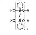
Fig. 1 has shown the chemical structure of PPSQ scalariform inorganic polymer (HO-PPSQ-H);
Fig. 2 has shown the comparison of the field emission I-V of standard C NT and PPSQ CNT negative electrode;
Fig. 3 has shown the PPSQ CNT negative electrode that is activated by band;
Fig. 4 has shown the PPSQ CNT negative electrode that is activated by the X film;
Fig. 5 has shown that the field emission I-V between the PPSQ CNT negative electrode of 200 ℃ and 450 ℃ lower curing compares;
Fig. 6 A and 6B have shown and are packed in the audion body cavity and solidify to form liquid polymers (X film water solution) for the peelable thick film that activates;
Fig. 7 has shown by adopting the X film to activate the homogeneous field emission image that obtains at the audion body with 50 microns deep holes;
Fig. 8 A-8I has shown with peelable film and forms pattern with high resolving power and activate the method for CNT negative electrode;
Fig. 9 has shown the according to the embodiment of the present invention field emission device of configuration; And
Figure 10 has shown the according to the embodiment of the present invention data handling system of configuration.
Detailed Description Of The Invention
In the following description, many concrete detailed descriptions (such as specific cathode material etc.) have been provided so that complete understanding of the present invention to be provided.Yet for those of ordinary skills, it is apparent can not adopting these specific specific descriptions in the practice of the present invention.In other cases, for avoiding making the present invention obscure because giving unnecessary details, adopted the block diagram form to show the circuit of knowing.For most parts, omitted the detailed description that relates to timing considerations (timing consideration) etc., this describes in detail for being not essential to complete understanding of the present invention because of these, and falls within the technical ability that those of ordinary skill in the related art possess.
Description, wherein described element not necessarily is shown to scale, and the identical or like in a plurality of views indicates with identical reference number.
Someone has proposed to adopt liquid polymer materials (U.S patent publication No. 2005/0129858A1, on June 16th, 2005) to come the cavity filling structure, and activates described CNT negative electrode at the polymeric film that solidifies when cathode surface is peeled off.Liquor is easy to infiltrate through in the porous C NT negative electrode, if the therefore imperfect words of adhesivity of CNT (for example with the CNT thickener by the sample that sprays and silk screen printing makes), most of cathode material will be easy to be removed.Because polymkeric substance has high-adhesiveness, can adopt inorganic powder to come the adhesion characteristics of telomerized polymer, when avoiding peeling off this polymer materials to CNT negative electrode injury.Yet, because inorganic powder is easy to sink to the bottom of polymkeric substance and is difficult for evenly being suspended in the solution, be difficult to inorganic powder is evenly dispersed in the polymkeric substance.Thus, the heterogeneity of powder divides breaking up to cause it to have inhomogenous adhesion characteristics when polymeric film solidifies.This will cause the unhomogeneity by the CNT negative electrode field emission that contains the activation of powder polymer film.But, if can improve the adhesivity of CNT negative electrode, just pure polymers soln can be used for the activation of homogeneous, and needn't remove too much CNT cathode material or damage CNT negative electrode.
The CNT thickener usually comprises organic or inorganic adhesive, solvent and other additive.When the clinkering process melts powder (frit material) with bonding substrate, often glass frit powder is used as inorganic adhesive so that CNT adheres on the substrate.Unfortunately, be essentially metal oxide powder (PbO, SiC2And B2O3Deng) frit base glass CNT can not be firmly bonded on the substrate, this is because powder covers on the substrate discontinuously after the uncompatibility of CNT and powder and the clinkering.The discontinuous covering of powder has also caused CNT to adhere to inhomogenous problem, and this is that the heterogeneity of CNT material is removed because heterogeneity adhesion on large area substrates is can cause applying activation process the time.In order to improve the adhesivity of CNT negative electrode, need to prepare the CNT thickener with the material that CNT and substrate is all had relatively strong bonding strength.Reported with spin glass (spin-on glass) tackiness agent (SOG) and other organic carrier and prepared the CNT thickener to improve field emission characteristics (Jae-Hong Park etc., Asian Display/IMID ' 04Digest, 468,2004).But, also have the outgas problem even if studies show that the SOG material after curing, this point is unfavorable for that this material becomes good candidate (J.D.Romero, M.Khan, H.Fatemi and J.Turlo, the J.Mater.Res. for vacuum apparatus, 6 (9), 1996 (1991)).Another problem that the CNT thickener meets with is usually need to come organic materials in the burn off thickener with high-temperature sintering process.The common meeting of this clinkering process is so that the field emission characteristics of CNT is deteriorated; this be damaged by CNT and thickener in organic support material produced the residue that affects CNT work function (workfunction) and caused (R.Collazo; R.Schlesser; and Z.Sitar; Appl.Phys.Lett.78,2058 (2001)).For the fusion bonded temperature with the CNT negative electrode is reduced to 360 ℃, the organic binder bond that can fire at low temperatures is studied (Sora Lee, Won Bin Im, Jong Hyuk Kang and DukYoung Jeon, J.Vac.Sci.Technol.B 23 (2), and 745 (2005)).But still need to improve with glass powder the adhesivity of CNT negative electrode.Yet unfortunately, still can detect the lower concentration retained material that is produced by organic binder bond after the clinkering.When causing transmitter then and there and being vacuum seal, the residue that is produced by organic materials also can cause the outgas problem.The organosiloxane polymer that is used as the low-temperature curing jointing material among the U.S. Patent Publication No. US2005/0242344 still needs to surpass 400 ℃ burn-out temperatures, and is to produce retained material.In the CNT paste formulation, need to solidify at low temperatures and can not make the deteriorated new jointing material of CNT.This jointing material also need have high high-temp stability, rough vacuum outgas and to the good dispersion of CNT.
Silicon ladder-like polymer, polyphenylsilsesquioxane (polyphenylsilsesquioxane, PPSQ) is a kind of inorganic polymer, it has cis-syndiotactic duplex structure (little J.F. Blang, J.Polym.Sci.1C (1963) 83) as shown in Figure 1.It becomes the material of new generation of, spaceship exterior coating bonding for semiconducting insulation film, optical fiber and moisture barrier coatings gradually.With this design of material for having SiO2Good physical properties and have reactive selection of relevant with organic chemistry good functional group chemistry.Particularly, because polyphenylsilsesquioxane ((C6H5SiO1.5) x) be the potential substitute that is used at present the silica-based inorganics of electronics, photoelectronics and other material technology, and have consistency with silica-based inorganics, it has received a large amount of concerns.PPSQ material with rough vacuum outgas characteristic be considered to be a kind of can with the isolator of the substrate excellent bonds that is used for field emission device (K.Nishimura, etc., J.Vac.Sci.Techn.B 22 (3), 1377 (2004)).The gas that the PPSQ type absorbs is quite low, is conducive to thus the long life of vacuum seal device.Can be with PPSQ as being used for microelectronic electrolyte with good adhesion, spinning applies or silk screen printing is on-chip thin and thick film.Such material also has low heat-shrinkable.The shrinking percentage of thermal annealing is less than 0.1%.In addition, can come so that the PPSQ material forms pattern by wet and dry etching.Different from glass frit powder is, the PPSQ material dissolves in solvent becomes solution, thereby so that CNT can be dispersed in the adhesivity adhesive matrix to obtain on-chip homogeneous adhesion layer.This material can be 200 ℃ of curing, and have thermostability up to 500 ℃ the time, and this just makes it become in CNT preparation instead of glass powder or even the excellent bonds agent candidate product of organic adhesive material.PPSQ type polymkeric substance can pass through other chemical functional group, for example C2H5O-PPSQ-C2H5And CH3-PPSQ-CH3, carry out the end combination.
Another kind of inorganic polymer---polyhedral oligomeric silsesquioxane (Polyhedral oligomericsilsesquioxane, POSS) also can be used in the CNT paste formulation.The POSS chemical technology has unique feature: its chemical constitution is silicon-dioxide (SiO2) and silicone (R2SiO) the intermediate (RSiO that mixes1.5).
PPSQ CNT paste formulation 1:
By with agitator mixing 40-50wt.%PPSQ material and 40-50wt.%toluene 15 hours, prepare the PPSQ material.The viscosity of PPSQ can be 500-5000CP.Then following preparation PPSQ CNT thickener:
Manual blending 20-30wt.%PPSQ+60-70wt.% thinner in mortar (Terpineol 350, tepineol)+3-10wt.%SWNT+3-10wt.% graphite (2-15 micron).Then, process thismixture 5 times with three-roll mill.Add Graphite Powder 99 and be in order to produce the border, thereby so that CNT can not imbed the PPSQ material fully, and guarantee that part CNT can be released (free) in activation process.
Available mesh screen is printed onto PPSQ CNT thickener on the ito glass.Active CNT cathode area can be 3 * 3cm2Fire PPSQ CNT negative electrode (400 ℃, in the nitrogen) with roasting method.The CNT negative electrode has extraordinary adhesivity, and this is because have foam sheet so that almost can not remove material from the surface of this negative electrode.Adhesive tape activates PPSQ CNT negative electrode is worked, and get on except considerably less material from the surface, and before and after activating, thickness (~7 microns) remains unchanged.When flexible foams and adhesive tape are used for activating, can adopt laminating machine, by the roller with suitable pressure foams or (viscose glue) band are applied on the surface of CNT negative electrode.Compare with other CNT negative electrode for preparing with the thickener that contains frit and organic carrier, PPSQ CNT negative electrode has much better adhesivity to substrate.For other carbon nanotube cathod that contains frit or other tackiness agent, when implementing adhesive tape activation process, the material more than 50% can be removed.Fig. 2 has shown the I-V curve of two kinds of PPSQ CNT negative electrodes and a kind of standard C NT negative electrode.Standard C NT thickener comprises CNT, organic carrier, frit and solvent.
Because PPSQ base CNT negative electrode has higher adhesivity, used water based polyalcohol (available from the X-film replica X2020 of transfer equipment company) activates the CNT negative electrode.This water polymeric solution comprises 56-78wt.% water, 17-34wt.% ethanol, 3-8wt.% ethanol homopolymer and 1-2wt.% butanols (buthl alcohol).Activation process is as follows:
1) a drop of liquid polymkeric substance (X-film) solution is placed on the CNT negative electrode.This liquor inundates whole negative electrodes equably.
2) at 60 ℃ baking oven or air drying X-film.Volume that can be by regulating the X-coating solution with the gauge control of X-film more than 50 microns.
3) peel off the X-film to activate the CNT negative electrode.
Liquor is easy to infiltrate through in the porous C NT negative electrode, if the therefore imperfect words of adhesivity of CNT (for example by the sample of spraying preparation and the sample of some printing), most of cathode material will be removed.The X-film activates good for the printing PPSQ CNT cathodic process with good adhesion.Standard C NT negative electrode is fired under 450 ℃ and can be with or foams activate, but the X-film has then been removed nearly all CNT cathode material, owing to stay the considerably less non-constant of field emission that causes of on-chip CNT.Different from the polymer materials of complexity used among the U.S. Patent Publication No. US2005/0129858A1, the X-film is a kind of water-soluble polymers and can at room temperature hardens in air.Because PPSQ CNT thickener has much better adhesivity compared with the CNT thickener of routine, PPSQ CNT thickener also is very unique.
The advantage that adopts the X-film to activate:
1) the pore structure substrate during triode is used can be filled naturally by liquor, and generation contacts with the homogeneous of CNT cathode surface in the hole.
2) adopt the activation of laminating machine on large negative electrode, usually can produce pressure change, caused thus inhomogenous problem.The X-film activates and can need not to adopt laminating machine.
3) owing to formed whole polymer sheet after solidifying, do not observe obvious residue at negative electrode after therefore activating.With band, tackiness agent (adhesive) separates with ductile basement, and some tackiness agent residues can be stayed on the negative electrode.
As shown in Figure 2, the PPSQ CNT negative electrode that activates with the X-film has the field emission characteristics of improvement.Fig. 3 shows the field emission illumination of the PPSQ CNT negative electrode (30mA, 4.2V/ micron) that is activated by band.Fig. 4 has shown the field emission illumination of the PPSQ CNT negative electrode (30mA, 3.9V/ micron) that is activated by the X-film.
PPSQ CNT paste formulation 2:
Also available double-walled CNT (DWNT) prepares the CNT thickener.Manual blending 15-25wt.%PPSQ (take toluene as solvent), 65-80wt.% thinner, 2-10wt.%DWNT and 2-10% graphite (2-15 micron) in mortar.Then, process this mixture at least 5 times with three-roll mill.
Available mesh screen is printed onto PPSQ CNT thickener that (active CNT cathode area can be 3 * 3cm on the ito glass2).Make PPSQ CNT negative electrode solidify (in 200 ℃ of air) 1 hour by bake process.This CNT negative electrode has good adhesivity.Band activates PPSQ CNT negative electrode is worked, and only gets on from the surface except few material, and thickness is basically constant before and after activating.Fig. 5 has shown the I-V curve of 200 ℃ of lower curing and 450 ℃ of lower PPSQCNT negative electrodes that solidify.It is deteriorated that this has shown that the curing of lesser temps exempts from CNT, produced thus lower electric field.
PPSQ CNT paste formulation 3:
Also PPSQ can be added other CNT thickener to improve adhesivity.Can with double-walled CNT (DWNT) thickener with the thickener of deciding, prepare with the 5-15wt.%PPSQ material.Can main DWNT thickener and 10-20wt.%CNT, 30-65wt.% organic carrier, 30-60wt.% thinner and 5-20wt.% glass frit is formulated together.Available pestle is admixed this mixture in mortar, and then further disperses to grind with three-roll mill.In process for preparation, can add the viscosity that thinner (Terpineol 350) is regulated this thickener.The viscosity of thickener can be 9000CP-90,000 centipoise (CP).
PPSQ CNT paste formulation 4:
Manual blending 10-30wt.%PPSQ+40-70wt.% thinner (Terpineol 350)+3-10wt.%SWNT+ (6-20wt.%) organic carrier+3-20wt.% graphite (2-15 micron) in mortar.Organic carrier comprises ethyl cellulose (15-20%), butylacetic acid carbitol ester (60-70%) and diethylene glycol monobutyl ether (10-20%).Then, process thismixture 5 times with three-roll mill.The viscosity of this thickener can be 10000CP-90000 centipoise (CP).Can under 390 ℃, fire the CNT negative electrode with this paste formulation preparation, with the organic support material that burnouts.The effect of the solid support material in the said preparation is so that PPSQ base thickener is more suitable for printing.
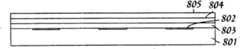
As shown in Figure 6, will be screen-printed on the triode material bodies with 50 μ m deep holes with the CNT thickener of PPSQ improvement with screen cloth.Fig. 6 A has shown the substrate 4 that has depositedelectrode 3 and isolator 2, forms pattern with the CNT negative electrode 1 that is deposited in the audion body opening on substrate 4.Fig. 6 B has shown the peelablepolymeric film 5 with the fluent material formation of X-film.Liquid polymers (aqueous solution of X-film) is packed in the cavity of triode material bodies, it is solidify to form for the peelable thick film that activates CNT negative electrode 1 (surpassing 50 μ m).
As shown in Figure 7, adopt the X-film to activate, can obtain to have the CNT negative electrode of the very homogeneous in dark chamber.Fig. 7 has shown the digital picture of field emission illumination, has illustrated at the audion body with 50 μ m deep holes to adopt X-film activation method (as shown in Figure 6) can obtain the very field emission of homogeneous.In this embodiment, pixel size is 250 * 800 μ m2
Adopt the CNT negative electrode of the formation high-resolution image of PPSQ CNT thickener and X-film:
The resolution limit of silk screen printing makes it be difficult to obtain feature less than the pattern of 50 μ m.Can adopt UV (UV-light) sensitive polymer to come to form pattern for CNT.Unfortunately, this polymer materials has residue after curing, and also needs an activation process after the CNT negative electrode forms pattern.In addition, usually need lift-off process to remove the zone that is exposed to UV.In this lift-off process, usually use the solvent that can affect the CNT negative electrode.Proved that the lithography that can adopt standard is that peelable X-film forms pattern.Below disclosed the method that adopts peelable film, available quite high resolving power is that the CNT negative electrode forms pattern, also can activate (as shown in Figure 8) when removing peelable film.Owing to can relatively high rate of etch come etching PPSQ material, can adopt RIE (reactive ion etching) with CF4And O2Etching PPSQ CNT negative electrode.Among Fig. 8 A, with electrodeposition on substrate.In Fig. 8 B, printing PPSQ CNT negative electrode is to continue this process.Fig. 8 C has shown that spinning is coated in the X-film of cathode top.Fig. 8 D has shown the photo-resist that is positioned at X-rete top.In Fig. 8 E, form pattern to continue this process at photo-resist in a desired manner.In Fig. 8 F, expose and with the litho technology removal X-film of photo-resist with routine.In Fig. 8 G, adopt dry etching to remove the PPSQ CNT cathode material that exposes.In Fig. 8 H, then deposition of thick X-film in Fig. 8 I, peels off thick X-film to activate the CNT negative electrode of patterning.
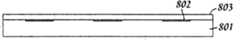
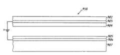
Fig. 9 has shown the as mentioned part of the field-emitter display 938 of the negative electrode preparation of manufacturing of use-case.Compriseconductive layer 906 in the negative electrode.Anode can compriseglass substrate 902,indium tin layer 903 and fluorescent layer 904.Between anode and negative electrode, electric field is set.This indicatingmeter 938 for example can be used in as shown in figure 10 thedata handling system 1013.
Figure 10 A has described to be used for putting into practice representative hardware environment of the present invention, the exemplary hardware arrangement that has showndata handling system 1013 of the present invention, it has central processing unit (CPU) 1010 (for example conventional microprocessor) and passes throughsystem bus 1012 interconnective a plurality of other unit.Data handling system 1013 comprises random access memory (RAM) 1014, read-only storage (ROM) 1016, be used for surrounding devices (forexample disk pack 1020 and tape drive 1040) is connected to I/O (I/O) adapter ofbus 1012, withkeyboard 1024,mouse 1026 and/or other interfacing equipment (for example unshowned touch-screen equipment) are connected to theuser interface adapter 1022 ofbus 1012,data handling system 1013 is connected to thecommunication adapter 1034 of data processing network, and thedisplay adapter 1036 thatbus 1012 is connected to display equipment 1038.CPU 1010 can comprise other circuit not shown in this figure, and it can comprise circuit common in the microprocessor, such as execution unit, Bus Interface Unit, mathematical logic unit etc.
Although described the present invention and advantage thereof in detail, should understand and not break away from the spirit and scope of the invention ground that is limited by claims and carry out various variations, replacement and change.
Claims (4)
Translated fromChineseApplications Claiming Priority (5)
| Application Number | Priority Date | Filing Date | Title |
|---|---|---|---|
| US75597806P | 2006-01-03 | 2006-01-03 | |
| US60/755,978 | 2006-01-03 | ||
| US11/612,313 | 2006-12-18 | ||
| US11/612,313US8264137B2 (en) | 2006-01-03 | 2006-12-18 | Curing binder material for carbon nanotube electron emission cathodes |
| PCT/US2006/062396WO2007111748A2 (en) | 2006-01-03 | 2006-12-20 | Curing binder material for carbon nanotube electron emission cathodes |
Publications (2)
| Publication Number | Publication Date |
|---|---|
| CN101365735A CN101365735A (en) | 2009-02-11 |
| CN101365735Btrue CN101365735B (en) | 2013-01-23 |
Family
ID=38541602
Family Applications (1)
| Application Number | Title | Priority Date | Filing Date |
|---|---|---|---|
| CN2006800502410AExpired - Fee RelatedCN101365735B (en) | 2006-01-03 | 2006-12-20 | Cured binder materials for carbon nanotube electron emission cathodes |
Country Status (6)
| Country | Link |
|---|---|
| US (1) | US8264137B2 (en) |
| JP (1) | JP2009522203A (en) |
| KR (1) | KR101368255B1 (en) |
| CN (1) | CN101365735B (en) |
| TW (1) | TWI449664B (en) |
| WO (1) | WO2007111748A2 (en) |
Families Citing this family (47)
| Publication number | Priority date | Publication date | Assignee | Title |
|---|---|---|---|---|
| KR101166015B1 (en)* | 2006-04-26 | 2012-07-19 | 삼성에스디아이 주식회사 | An electron emission source, a composition for preparing an electron emission source, a method for preparing the electron emission source and an electron emission device comprising the electron emission source |
| CN101470566B (en)* | 2007-12-27 | 2011-06-08 | 清华大学 | Touch control device |
| CN101458594B (en)* | 2007-12-12 | 2012-07-18 | 清华大学 | Touch screen and display device |
| CN101470558B (en)* | 2007-12-27 | 2012-11-21 | 清华大学 | Touch screen and display equipment |
| CN101655720B (en)* | 2008-08-22 | 2012-07-18 | 清华大学 | Personal digital assistant |
| CN101458600B (en)* | 2007-12-14 | 2011-11-30 | 清华大学 | Touch screen and display device |
| CN101458604B (en)* | 2007-12-12 | 2012-03-28 | 清华大学 | Touch screen and display device |
| CN101458606B (en)* | 2007-12-12 | 2012-06-20 | 清华大学 | Touch screen, method for producing the touch screen, and display device using the touch screen |
| CN101458595B (en)* | 2007-12-12 | 2011-06-08 | 清华大学 | Touch screen and display device |
| CN101470560B (en)* | 2007-12-27 | 2012-01-25 | 清华大学 | Touch screen and display equipment |
| CN101458598B (en)* | 2007-12-14 | 2011-06-08 | 清华大学 | Touch screen and display device |
| CN101676832B (en)* | 2008-09-19 | 2012-03-28 | 清华大学 | Desktop PC |
| CN101656769B (en)* | 2008-08-22 | 2012-10-10 | 清华大学 | Mobile telephone |
| CN101458608B (en)* | 2007-12-14 | 2011-09-28 | 清华大学 | Touch screen preparation method |
| CN101464763B (en)* | 2007-12-21 | 2010-09-29 | 清华大学 | Manufacturing method of touch screen |
| CN101458597B (en)* | 2007-12-14 | 2011-06-08 | 清华大学 | Touch screen, method for producing the touch screen, and display device using the touch screen |
| CN101458602B (en)* | 2007-12-12 | 2011-12-21 | 清华大学 | Touch screen and display device |
| CN101470559B (en)* | 2007-12-27 | 2012-11-21 | 清华大学 | Touch screen and display equipment |
| CN101458603B (en)* | 2007-12-12 | 2011-06-08 | 北京富纳特创新科技有限公司 | Touch screen and display device |
| CN101458593B (en)* | 2007-12-12 | 2012-03-14 | 清华大学 | Touch screen and display device |
| CN101419519B (en)* | 2007-10-23 | 2012-06-20 | 清华大学 | Touch panel |
| CN101620454A (en)* | 2008-07-04 | 2010-01-06 | 清华大学 | Potable computer |
| CN101458609B (en)* | 2007-12-14 | 2011-11-09 | 清华大学 | Touch screen and display device |
| CN101458605B (en)* | 2007-12-12 | 2011-03-30 | 鸿富锦精密工业(深圳)有限公司 | Touch screen and display device |
| CN101419518B (en)* | 2007-10-23 | 2012-06-20 | 清华大学 | Touch panel |
| CN101458599B (en)* | 2007-12-14 | 2011-06-08 | 清华大学 | Touch screen, method for producing the touch screen, and display device using the touch screen |
| CN101458596B (en)* | 2007-12-12 | 2011-06-08 | 北京富纳特创新科技有限公司 | Touch screen and display device |
| CN101458975B (en)* | 2007-12-12 | 2012-05-16 | 清华大学 | Electronic element |
| CN101458601B (en)* | 2007-12-14 | 2012-03-14 | 清华大学 | Touch screen and display device |
| CN101464757A (en)* | 2007-12-21 | 2009-06-24 | 清华大学 | Touch screen and display equipment |
| CN101458607B (en)* | 2007-12-14 | 2010-12-29 | 清华大学 | Touch screen and display device |
| CN101464765B (en)* | 2007-12-21 | 2011-01-05 | 鸿富锦精密工业(深圳)有限公司 | Touch screen and display equipment |
| CN101470565B (en)* | 2007-12-27 | 2011-08-24 | 清华大学 | Touch screen and display device |
| CN101464764B (en)* | 2007-12-21 | 2012-07-18 | 清华大学 | Touch screen and display equipment |
| US8574393B2 (en)* | 2007-12-21 | 2013-11-05 | Tsinghua University | Method for making touch panel |
| CN101464766B (en)* | 2007-12-21 | 2011-11-30 | 清华大学 | Touch screen and display equipment |
| US8237677B2 (en)* | 2008-07-04 | 2012-08-07 | Tsinghua University | Liquid crystal display screen |
| US8390580B2 (en) | 2008-07-09 | 2013-03-05 | Tsinghua University | Touch panel, liquid crystal display screen using the same, and methods for making the touch panel and the liquid crystal display screen |
| CN101924816B (en)* | 2009-06-12 | 2013-03-20 | 清华大学 | Flexible mobile phone |
| CN102013371B (en)* | 2009-09-04 | 2012-11-21 | 清华大学 | Surface treatment method for cold cathode |
| TWI407485B (en)* | 2009-09-22 | 2013-09-01 | Hon Hai Prec Ind Co Ltd | Method for treating surface of cold cathode |
| CN102443247B (en)* | 2011-09-16 | 2013-01-23 | 桂林理工大学 | Preparation method of graphene oxide grafted POSS (polyhedral oligomeric silsesquioxane) modified epoxy resin |
| JP6700787B2 (en)* | 2012-12-07 | 2020-05-27 | スリーエム イノベイティブ プロパティズ カンパニー | Method for producing transparent conductor on substrate |
| JP5881019B2 (en)* | 2013-03-07 | 2016-03-09 | 国立大学法人 鹿児島大学 | Carbon nanotube dispersant, method for producing the same, carbon nanotube dispersion, and method for producing the same |
| JP6487740B2 (en)* | 2014-04-07 | 2019-03-20 | 株式会社日本触媒 | Polysiloxane compound, method for producing the same, and conductive carbon material-containing composition comprising polysiloxane compound and conductive carbon material |
| CN105448624B (en)* | 2014-07-10 | 2017-09-01 | 清华大学 | Preparation method of field emission cathode |
| CN111128637B (en)* | 2018-11-01 | 2021-02-26 | 清华大学 | Method for making field emitters |
Family Cites Families (184)
| Publication number | Priority date | Publication date | Assignee | Title |
|---|---|---|---|---|
| US5458784A (en) | 1990-10-23 | 1995-10-17 | Catalytic Materials Limited | Removal of contaminants from aqueous and gaseous streams using graphic filaments |
| US5547748A (en) | 1994-01-14 | 1996-08-20 | Sri International | Carbon nanoencapsulates |
| US5691101A (en) | 1994-03-15 | 1997-11-25 | Kabushiki Kaisha Toshiba | Photosensitive composition |
| US5866434A (en) | 1994-12-08 | 1999-02-02 | Meso Scale Technology | Graphitic nanotubes in luminescence assays |
| US6203814B1 (en) | 1994-12-08 | 2001-03-20 | Hyperion Catalysis International, Inc. | Method of making functionalized nanotubes |
| US6673533B1 (en) | 1995-03-10 | 2004-01-06 | Meso Scale Technologies, Llc. | Multi-array multi-specific electrochemiluminescence testing |
| CA2704228C (en) | 1995-03-10 | 2013-10-22 | Meso Scale Technologies, Llc | Multi-array, multi-specific electrochemiluminescence testing |
| US5512368A (en) | 1995-03-16 | 1996-04-30 | E. I. Du Pont De Nemours And Company | Fibers reinforced with inorganic whiskers |
| JPH09111135A (en) | 1995-10-23 | 1997-04-28 | Mitsubishi Materials Corp | Conductive polymer composition |
| US5800706A (en) | 1996-03-06 | 1998-09-01 | Hyperion Catalysis International, Inc. | Nanofiber packed beds having enhanced fluid flow characteristics |
| US5965202A (en) | 1996-05-02 | 1999-10-12 | Lucent Technologies, Inc. | Hybrid inorganic-organic composite for use as an interlayer dielectric |
| US6017390A (en) | 1996-07-24 | 2000-01-25 | The Regents Of The University Of California | Growth of oriented crystals at polymerized membranes |
| DE69728410T2 (en) | 1996-08-08 | 2005-05-04 | William Marsh Rice University, Houston | MACROSCOPICALLY MANIPULATED DEVICES MANUFACTURED FROM NANOROE ASSEMBLIES |
| US6713173B2 (en) | 1996-11-16 | 2004-03-30 | Nanomagnetics Limited | Magnetizable device |
| US6683783B1 (en) | 1997-03-07 | 2004-01-27 | William Marsh Rice University | Carbon fibers formed from single-wall carbon nanotubes |
| US6770583B2 (en) | 1997-03-14 | 2004-08-03 | The United States Of America As Represented By The Secretary Of The Navy | Transistion metal containing ceramic with metal nanoparticles |
| US6205016B1 (en) | 1997-06-04 | 2001-03-20 | Hyperion Catalysis International, Inc. | Fibril composite electrode for electrochemical capacitors |
| DE19745549C2 (en) | 1997-10-10 | 1999-11-04 | Mannesmann Ag | Gas storage |
| US6126888A (en) | 1998-01-09 | 2000-10-03 | Quantum Group Inc. | Method for making strong mantles and other ceramic structures |
| US6287765B1 (en) | 1998-05-20 | 2001-09-11 | Molecular Machines, Inc. | Methods for detecting and identifying single molecules |
| US6705152B2 (en) | 2000-10-24 | 2004-03-16 | Nanoproducts Corporation | Nanostructured ceramic platform for micromachined devices and device arrays |
| DE19859654A1 (en) | 1998-12-15 | 2000-06-29 | Mannesmann Ag | Device for storing compressed gas |
| EP1144197B1 (en) | 1999-01-15 | 2003-06-11 | 3M Innovative Properties Company | Thermal Transfer Method. |
| US6555945B1 (en) | 1999-02-25 | 2003-04-29 | Alliedsignal Inc. | Actuators using double-layer charging of high surface area materials |
| US6333016B1 (en) | 1999-06-02 | 2001-12-25 | The Board Of Regents Of The University Of Oklahoma | Method of producing carbon nanotubes |
| US6444864B1 (en) | 1999-06-07 | 2002-09-03 | Drexel University | Thermal plasma process for recovering monomers and high value carbons from polymeric materials |
| EP2224508B1 (en) | 1999-07-02 | 2016-01-06 | President and Fellows of Harvard College | Method of separating metallic and semiconducting nanoscopic wires |
| DE10023456A1 (en) | 1999-07-29 | 2001-02-01 | Creavis Tech & Innovation Gmbh | Mesotubes and nanotubes |
| US6299812B1 (en) | 1999-08-16 | 2001-10-09 | The Board Of Regents Of The University Of Oklahoma | Method for forming a fibers/composite material having an anisotropic structure |
| US6723396B1 (en) | 1999-08-17 | 2004-04-20 | Western Washington University | Liquid crystal imprinting |
| US6423768B1 (en) | 1999-09-07 | 2002-07-23 | General Electric Company | Polymer-organoclay composite compositions, method for making and articles therefrom |
| US6491891B1 (en) | 1999-09-10 | 2002-12-10 | Ut-Battelle, Inc. | Gelcasting polymeric precursors for producing net-shaped graphites |
| US6517995B1 (en) | 1999-09-14 | 2003-02-11 | Massachusetts Institute Of Technology | Fabrication of finely featured devices by liquid embossing |
| JP3834746B2 (en) | 1999-09-22 | 2006-10-18 | 潤二 伊藤 | Porous rubber electrode binder, porous rubber electrode using the same, and porous rubber electrode substrate |
| US6318649B1 (en) | 1999-10-06 | 2001-11-20 | Cornerstone Technologies, Llc | Method of creating ultra-fine particles of materials using a high-pressure mill |
| AU1614101A (en) | 1999-11-18 | 2001-05-30 | Advanced Technology Materials, Inc. | Optical hydrogen detector |
| US6352782B2 (en) | 1999-12-01 | 2002-03-05 | General Electric Company | Poly(phenylene ether)-polyvinyl thermosetting resin |
| US6401526B1 (en) | 1999-12-10 | 2002-06-11 | The Board Of Trustees Of The Leland Stanford Junior University | Carbon nanotubes and methods of fabrication thereof using a liquid phase catalyst precursor |
| US6521703B2 (en) | 2000-01-18 | 2003-02-18 | General Electric Company | Curable resin composition, method for the preparation thereof, and articles derived thereform |
| AU3229901A (en) | 2000-02-16 | 2001-08-27 | Asahi Kasei Kabushiki Kaisha | Polyamide resin composition |
| US6979248B2 (en) | 2002-05-07 | 2005-12-27 | Applied Materials, Inc. | Conductive polishing article for electrochemical mechanical polishing |
| US6991528B2 (en) | 2000-02-17 | 2006-01-31 | Applied Materials, Inc. | Conductive polishing article for electrochemical mechanical polishing |
| US6800155B2 (en) | 2000-02-24 | 2004-10-05 | The United States Of America As Represented By The Secretary Of The Army | Conductive (electrical, ionic and photoelectric) membrane articlers, and method for producing same |
| US6414086B1 (en) | 2000-02-29 | 2002-07-02 | Howmedica Osteonics Corp. | Compositions, processes and methods of improving the wear resistance of prosthetic medical devices |
| US6610351B2 (en) | 2000-04-12 | 2003-08-26 | Quantag Systems, Inc. | Raman-active taggants and their recognition |
| US6894100B2 (en) | 2000-04-26 | 2005-05-17 | Asahi Kasei Kabushiki Kaisha | Electrically conductive resin composition and production process thereof |
| US6706963B2 (en) | 2002-01-25 | 2004-03-16 | Konarka Technologies, Inc. | Photovoltaic cell interconnection |
| US6913713B2 (en) | 2002-01-25 | 2005-07-05 | Konarka Technologies, Inc. | Photovoltaic fibers |
| US6919119B2 (en) | 2000-05-30 | 2005-07-19 | The Penn State Research Foundation | Electronic and opto-electronic devices fabricated from nanostructured high surface to volume ratio thin films |
| US6384727B1 (en) | 2000-08-02 | 2002-05-07 | Motorola, Inc. | Capacitively powered radio frequency identification device |
| AU8543901A (en) | 2000-08-15 | 2002-02-25 | Univ Pennsylvania | Directed assembly of nanometer-scale molecular devices |
| US7094285B2 (en) | 2000-09-20 | 2006-08-22 | Goodrich Corporation | Inorganic matrix compositions, composites incorporating the matrix, and process of making the same |
| CN1187596C (en) | 2000-09-21 | 2005-02-02 | 松下电器产业株式会社 | Scanning type probe microscope probe and method of producing the same, and scanning type probe microscope having this probe and polymer processing method using the same |
| US6861481B2 (en) | 2000-09-29 | 2005-03-01 | Solvay Engineered Polymers, Inc. | Ionomeric nanocomposites and articles therefrom |
| US7067577B2 (en) | 2000-10-16 | 2006-06-27 | Asahi Kasei Kabushiki Kaisha | Apatite-reinforced resin composition |
| US6893103B2 (en) | 2000-10-17 | 2005-05-17 | Seiko Epson Corporation | Ink jet recording apparatus and manufacturing method for functional liquid applied substrate |
| US6599446B1 (en) | 2000-11-03 | 2003-07-29 | General Electric Company | Electrically conductive polymer composite compositions, method for making, and method for electrical conductivity enhancement |
| US6682677B2 (en) | 2000-11-03 | 2004-01-27 | Honeywell International Inc. | Spinning, processing, and applications of carbon nanotube filaments, ribbons, and yarns |
| JP4887558B2 (en) | 2000-11-07 | 2012-02-29 | ソニー株式会社 | How to use the fuel cell |
| JP4267914B2 (en) | 2000-11-21 | 2009-05-27 | タイコ・エレクトロニクス・コーポレイション | Pigments and compositions used for laser marking |
| CA2430888C (en) | 2000-12-11 | 2013-10-22 | President And Fellows Of Harvard College | Nanosensors |
| US6783746B1 (en) | 2000-12-12 | 2004-08-31 | Ashland, Inc. | Preparation of stable nanotube dispersions in liquids |
| US6691505B2 (en) | 2001-01-10 | 2004-02-17 | Alliant Techsystems Inc. | Fiber-reinforced rocket motor insulation |
| WO2002066482A1 (en) | 2001-01-17 | 2002-08-29 | Purdue Research Foundation | Method and associated compounds for forming nanotubes |
| US6538725B2 (en) | 2001-01-22 | 2003-03-25 | General Electric Company | Method for determination of structural defects of coatings |
| US6782154B2 (en) | 2001-02-12 | 2004-08-24 | Rensselaer Polytechnic Institute | Ultrafast all-optical switch using carbon nanotube polymer composites |
| JP3809342B2 (en) | 2001-02-13 | 2006-08-16 | 喜萬 中山 | Light emitting / receiving probe and light emitting / receiving probe apparatus |
| EP1360700A1 (en) | 2001-02-16 | 2003-11-12 | E.I. Dupont de Nemours and Company | High conductivity polyaniline compositions and uses therefor |
| JP3991602B2 (en) | 2001-03-02 | 2007-10-17 | 富士ゼロックス株式会社 | Carbon nanotube structure manufacturing method, wiring member manufacturing method, and wiring member |
| EP1385481A4 (en) | 2001-03-26 | 2006-06-07 | Eikos Inc | Carbon nanotubes in structures and repair compositions |
| WO2002076724A1 (en) | 2001-03-26 | 2002-10-03 | Eikos, Inc. | Coatings containing carbon nanotubes |
| DE10116232A1 (en) | 2001-04-02 | 2002-10-10 | Creavis Tech & Innovation Gmbh | Molded articles with internally coated cavities, useful as e.g. sensors, are prepared by forming template fibers with selective removal of material |
| US6977171B1 (en) | 2001-04-03 | 2005-12-20 | University Of Florida | Detoxification and decontamination using nanotechnology therapy |
| WO2002081372A2 (en) | 2001-04-06 | 2002-10-17 | Carnegie Mellon University | A process for the preparation of nanostructured materials |
| US6689835B2 (en) | 2001-04-27 | 2004-02-10 | General Electric Company | Conductive plastic compositions and method of manufacture thereof |
| JP4207398B2 (en) | 2001-05-21 | 2009-01-14 | 富士ゼロックス株式会社 | Method for manufacturing wiring of carbon nanotube structure, wiring of carbon nanotube structure, and carbon nanotube device using the same |
| US7052854B2 (en) | 2001-05-23 | 2006-05-30 | University Of Florida Research Foundation, Inc. | Application of nanotechnology and sensor technologies for ex-vivo diagnostics |
| US6984678B2 (en) | 2001-05-24 | 2006-01-10 | Asahi Kasei Kabushiki Kaisha | Thermoplastic resin composition and molded articles |
| US6762237B2 (en) | 2001-06-08 | 2004-07-13 | Eikos, Inc. | Nanocomposite dielectrics |
| WO2003040446A2 (en) | 2001-06-15 | 2003-05-15 | The Pennsylvania State Research Foundation | Method of purifying nanotubes and nanofibers using electromagnetic radiation |
| US7077939B1 (en) | 2001-06-18 | 2006-07-18 | The Texas A&M University System | Method and apparatus for nanoparticle transport and detection |
| US6706402B2 (en) | 2001-07-25 | 2004-03-16 | Nantero, Inc. | Nanotube films and articles |
| US6919592B2 (en) | 2001-07-25 | 2005-07-19 | Nantero, Inc. | Electromechanical memory array using nanotube ribbons and method for making same |
| US6574130B2 (en) | 2001-07-25 | 2003-06-03 | Nantero, Inc. | Hybrid circuit having nanotube electromechanical memory |
| US6911682B2 (en) | 2001-12-28 | 2005-06-28 | Nantero, Inc. | Electromechanical three-trace junction devices |
| US6835591B2 (en) | 2001-07-25 | 2004-12-28 | Nantero, Inc. | Methods of nanotube films and articles |
| US6643165B2 (en) | 2001-07-25 | 2003-11-04 | Nantero, Inc. | Electromechanical memory having cell selection circuitry constructed with nanotube technology |
| US7118693B2 (en) | 2001-07-27 | 2006-10-10 | Eikos, Inc. | Conformal coatings comprising carbon nanotubes |
| JP2003045760A (en) | 2001-07-30 | 2003-02-14 | Asahi Glass Co Ltd | Multilayer electric double layer capacitor module |
| US6819845B2 (en) | 2001-08-02 | 2004-11-16 | Ultradots, Inc. | Optical devices with engineered nonlinear nanocomposite materials |
| JP2003050280A (en) | 2001-08-03 | 2003-02-21 | Konica Corp | Radiographic image detector |
| DE60238123D1 (en) | 2001-08-09 | 2010-12-09 | Asahi Chemical Ind | ORGANIC SEMICONDUCTOR LAYER AND METHOD FOR THE PRODUCTION THEREOF |
| US7001556B1 (en) | 2001-08-16 | 2006-02-21 | The Board Of Regents University Of Oklahoma | Nanotube/matrix composites and methods of production and use |
| US6566665B2 (en) | 2001-08-17 | 2003-05-20 | International Business Machines Corporation | Method and apparatus for linking and/or patterning self-assembled objects |
| DE60229955D1 (en) | 2001-08-29 | 2009-01-02 | Georgia Tech Res Inst | COMPOSITIONS COMPRISING STAINLESS POLYMERS AND NANOROUS STRUCTURES, AND METHOD FOR MANUFACTURING THE SAME |
| WO2003019586A1 (en) | 2001-08-30 | 2003-03-06 | Koninklijke Philips Electronics N.V. | Magnetoresistive device and electronic device |
| EP1291932A3 (en) | 2001-09-05 | 2006-10-18 | Konica Corporation | Organic thin-film semiconductor element and manufacturing method for the same |
| US6867295B2 (en) | 2001-09-07 | 2005-03-15 | Dionex Corporation | Ion exchange cryptands covalently bound to substrates |
| JP4729254B2 (en) | 2001-09-10 | 2011-07-20 | メソ スケイル テクノロジーズ,エルエルシー | Assay buffer, composition containing it, and method of use thereof |
| US6991876B2 (en) | 2001-10-05 | 2006-01-31 | Sri International | Metal/active oxygen batteries |
| DE60208288T2 (en) | 2001-10-15 | 2006-09-07 | Fuji Photo Film Co., Ltd., Minami-Ashigara | Lithographic printing plate precursor |
| US7074519B2 (en) | 2001-10-26 | 2006-07-11 | The Regents Of The University Of California | Molehole embedded 3-D crossbar architecture used in electrochemical molecular memory device |
| US20030134212A1 (en) | 2001-12-26 | 2003-07-17 | Eastman Kodak Company | Element with antistat layer |
| US6811724B2 (en) | 2001-12-26 | 2004-11-02 | Eastman Kodak Company | Composition for antistat layer |
| AUPR977301A0 (en) | 2001-12-28 | 2002-01-31 | Energy Storage Systems Pty Ltd | An electrode for an energy storage device |
| US6784028B2 (en) | 2001-12-28 | 2004-08-31 | Nantero, Inc. | Methods of making electromechanical three-trace junction devices |
| US6887450B2 (en) | 2002-01-02 | 2005-05-03 | Zyvex Corporation | Directional assembly of carbon nanotube strings |
| US6919395B2 (en) | 2002-01-04 | 2005-07-19 | Acushnet Company | Golf ball compositions comprising nanoparticulates |
| JP3453377B2 (en) | 2002-01-08 | 2003-10-06 | 科学技術振興事業団 | Carbon nanotube / carbon nanohorn composite and method for producing the same |
| US7037562B2 (en) | 2002-01-14 | 2006-05-02 | Vascon Llc | Angioplasty super balloon fabrication with composite materials |
| US7091412B2 (en) | 2002-03-04 | 2006-08-15 | Nanoset, Llc | Magnetically shielded assembly |
| US7115305B2 (en) | 2002-02-01 | 2006-10-03 | California Institute Of Technology | Method of producing regular arrays of nano-scale objects using nano-structured block-copolymeric materials |
| US6953001B2 (en) | 2002-02-04 | 2005-10-11 | Kazak Composites, Incorporated | Hatch or door system for securing and sealing openings in marine vessels |
| US6828015B2 (en) | 2002-02-08 | 2004-12-07 | Mitsubishi Gas Chemical Company, Inc. | Composite containing thin-film particles having carbon skeleton, method of reducing the thin-film particles, and process for the production of the composite |
| US6740900B2 (en) | 2002-02-27 | 2004-05-25 | Konica Corporation | Organic thin-film transistor and manufacturing method for the same |
| US7127294B1 (en) | 2002-12-18 | 2006-10-24 | Nanoset Llc | Magnetically shielded assembly |
| US7074310B2 (en) | 2002-03-04 | 2006-07-11 | William Marsh Rice University | Method for separating single-wall carbon nanotubes and compositions thereof |
| US7235912B2 (en) | 2002-03-08 | 2007-06-26 | Chien-Min Sung | Diamond-like carbon thermoelectric conversion devices and methods for the use and manufacture thereof |
| EP1493183B1 (en) | 2002-04-02 | 2012-12-05 | Dow Global Technologies LLC | Process for making air gap containing semiconducting devices and resulting semiconducting device |
| US6958192B2 (en) | 2002-04-05 | 2005-10-25 | The United States Of America As Represented By The Administrator Of The National Aeronautics And Space Administration | Polyimides from 2,3,3′,4′-biphenyltetracarboxylic dianhydride and aromatic diamines |
| EP1503956A1 (en) | 2002-04-08 | 2005-02-09 | William Marsh Rice University | Method for cutting single-wall carbon nanotubes through fluorination |
| US7122710B2 (en) | 2002-04-08 | 2006-10-17 | Wiiliam Marsh Rice University | Fluorination of polymeric C60 |
| US6879143B2 (en) | 2002-04-16 | 2005-04-12 | Motorola, Inc. | Method of selectively aligning and positioning nanometer-scale components using AC fields |
| EP1498456A4 (en) | 2002-04-22 | 2009-06-10 | Konica Corp | Organic semiconductor composition, organic semiconductor element, and process for producing the same |
| US6908261B2 (en) | 2002-05-09 | 2005-06-21 | Forward Ventures, Lp | Conductor polymer backfill composition and method of use as a reinforcement material for utility poles |
| EP1361619A3 (en) | 2002-05-09 | 2007-08-15 | Konica Corporation | Organic thin-film transistor, organic thin-film transistor sheet and manufacturing method thereof |
| AU2003229333A1 (en) | 2002-05-21 | 2003-12-12 | Eikos, Inc. | Method for patterning carbon nanotube coating and carbon nanotube wiring |
| US7122106B2 (en) | 2002-05-23 | 2006-10-17 | Battelle Memorial Institute | Electrosynthesis of nanofibers and nano-composite films |
| US6872330B2 (en) | 2002-05-30 | 2005-03-29 | The Regents Of The University Of California | Chemical manufacture of nanostructured materials |
| US6946597B2 (en) | 2002-06-22 | 2005-09-20 | Nanosular, Inc. | Photovoltaic devices fabricated by growth from porous template |
| JP3606855B2 (en) | 2002-06-28 | 2005-01-05 | ドン ウン インターナショナル カンパニー リミテッド | Method for producing carbon nanoparticles |
| US6852410B2 (en) | 2002-07-01 | 2005-02-08 | Georgia Tech Research Corporation | Macroscopic fiber comprising single-wall carbon nanotubes and acrylonitrile-based polymer and process for making the same |
| US7061749B2 (en) | 2002-07-01 | 2006-06-13 | Georgia Tech Research Corporation | Supercapacitor having electrode material comprising single-wall carbon nanotubes and process for making the same |
| US7098056B2 (en) | 2002-08-09 | 2006-08-29 | Nanoink, Inc. | Apparatus, materials, and methods for fabrication and catalysis |
| US7077891B2 (en) | 2002-08-13 | 2006-07-18 | Air Products And Chemicals, Inc. | Adsorbent sheet material for parallel passage contactors |
| JP4547852B2 (en) | 2002-09-04 | 2010-09-22 | 富士ゼロックス株式会社 | Manufacturing method of electrical parts |
| TW200425530A (en) | 2002-09-05 | 2004-11-16 | Nanosys Inc | Nanostructure and nanocomposite based compositions and photovoltaic devices |
| US6749982B2 (en) | 2002-09-27 | 2004-06-15 | Eastman Kodak Company | Imaging member with polyester base |
| US6881492B2 (en) | 2002-09-27 | 2005-04-19 | Eastman Kodak Company | Primer composition for polyesters |
| US7067867B2 (en) | 2002-09-30 | 2006-06-27 | Nanosys, Inc. | Large-area nonenabled macroelectronic substrates and uses therefor |
| JP4120527B2 (en) | 2002-10-04 | 2008-07-16 | 旭硝子株式会社 | Tetrafluoroethylene / ethylene copolymer composition |
| JP4458231B2 (en) | 2002-10-08 | 2010-04-28 | 三菱瓦斯化学株式会社 | Polyamide and resin composition |
| WO2004044552A2 (en) | 2002-11-12 | 2004-05-27 | Nanoink, Inc. | Methods and apparatus for ink delivery to nanolithographic probe systems |
| US7125533B2 (en) | 2002-11-15 | 2006-10-24 | William Marsh Rice University | Method for functionalizing carbon nanotubes utilizing peroxides |
| JP4327732B2 (en) | 2002-12-02 | 2009-09-09 | 三洋電機株式会社 | Solid polymer fuel cell and manufacturing method thereof |
| US7074887B2 (en) | 2002-12-17 | 2006-07-11 | The Regents Of The University Of California | Chemical synthesis of chiral conducting polymers |
| US6841213B2 (en) | 2002-12-27 | 2005-01-11 | Scimed Life Systems, Inc | Fiber pattern printing |
| US7244499B2 (en)* | 2003-01-10 | 2007-07-17 | Sanyo Electric Co., Ltd. | Bonded structure including a carbon nanotube |
| US6833201B2 (en) | 2003-01-31 | 2004-12-21 | Clemson University | Nanostructured-doped compound for use in an EL element |
| US6822032B2 (en) | 2003-02-06 | 2004-11-23 | General Electric Company | Impact modified compositions of polyimide and polyamide resins |
| JP2004288609A (en)* | 2003-03-06 | 2004-10-14 | Mitsubishi Electric Corp | Electron emission source, manufacturing method thereof, and image display device |
| US7075105B2 (en) | 2003-03-19 | 2006-07-11 | Masataka Kano | Organic bistable element, organic bistable memory device using the same, and method for driving said organic bistable element and organic bistable memory device |
| US6858528B2 (en) | 2003-03-20 | 2005-02-22 | Intel Corporation | Composite sacrificial material |
| JP4619624B2 (en) | 2003-03-31 | 2011-01-26 | 旭硝子株式会社 | Laminated hose |
| WO2005008706A2 (en) | 2003-04-01 | 2005-01-27 | Cabot Microelectronics Corporation | Electron source and method for making same |
| US6825060B1 (en) | 2003-04-02 | 2004-11-30 | Advanced Micro Devices, Inc. | Photosensitive polymeric memory elements |
| US7082683B2 (en) | 2003-04-24 | 2006-08-01 | Korea Institute Of Machinery & Materials | Method for attaching rod-shaped nano structure to probe holder |
| JP3999746B2 (en) | 2003-05-19 | 2007-10-31 | ローム アンド ハース カンパニー | Method for preparing high solid content of polymer nanoparticles |
| US6860956B2 (en) | 2003-05-23 | 2005-03-01 | Agency For Science, Technology & Research | Methods of creating patterns on substrates and articles of manufacture resulting therefrom |
| EP2422950B1 (en) | 2003-06-24 | 2014-10-01 | Aspen Aerogels Inc. | Methods to produce gel sheets |
| US7125101B2 (en) | 2003-07-30 | 2006-10-24 | Hewlett-Packard Development Company, L.P. | Photonically activated fluid ejector apparatus and methods |
| US7026432B2 (en) | 2003-08-12 | 2006-04-11 | General Electric Company | Electrically conductive compositions and method of manufacture thereof |
| US7083885B2 (en) | 2003-09-23 | 2006-08-01 | Eastman Kodak Company | Transparent invisible conductive grid |
| US6995266B2 (en) | 2003-10-03 | 2006-02-07 | General Electric Company | Thermally stable anthrapyridone compositions |
| US7119028B1 (en) | 2003-10-29 | 2006-10-10 | The United States Of America As Represented By The Secretary Of The Navy | Surface imprinted films with carbon nanotubes |
| US7122165B2 (en) | 2003-11-03 | 2006-10-17 | The Research Foundation Of State University Of New York | Sidewall-functionalized carbon nanotubes, and methods for making the same |
| US7013998B2 (en) | 2003-11-20 | 2006-03-21 | Halliburton Energy Services, Inc. | Drill bit having an improved seal and lubrication method using same |
| US7118652B2 (en) | 2003-12-04 | 2006-10-10 | General Motors Corporation | Airflow control devices based on active materials |
| US7059664B2 (en) | 2003-12-04 | 2006-06-13 | General Motors Corporation | Airflow control devices based on active materials |
| KR20050060287A (en) | 2003-12-16 | 2005-06-22 | 삼성에스디아이 주식회사 | Method for forming carbon nanotube emitter |
| US7056849B2 (en) | 2004-01-16 | 2006-06-06 | General Electric Company | Nanoscale ordered composites of covalent ceramics for high-temperature structural applications via block-copolymer-assisted assembly and method of making |
| US7052618B2 (en) | 2004-01-28 | 2006-05-30 | Agilent Technologies, Inc. | Nanostructures and methods of making the same |
| US6927249B1 (en) | 2004-02-11 | 2005-08-09 | Lg Chem, Ltd. | Heat absorb-release plastic resin composition and molded product thereof |
| US7086939B2 (en) | 2004-03-19 | 2006-08-08 | Saint-Gobain Performance Plastics Corporation | Chemical mechanical polishing retaining ring with integral polymer backing |
| KR20050096536A (en)* | 2004-03-31 | 2005-10-06 | 삼성에스디아이 주식회사 | Electron emission display with grid electrode |
| US7019391B2 (en) | 2004-04-06 | 2006-03-28 | Bao Tran | NANO IC packaging |
| KR20050104839A (en) | 2004-04-29 | 2005-11-03 | 삼성에스디아이 주식회사 | A method for preparing an emitter, an emitter and an electron emission device comprising the emitter |
| US7029056B2 (en) | 2004-06-09 | 2006-04-18 | General Motors Corporation | Closure lockdown assemblies and methods utilizing active materials |
| US6893895B1 (en) | 2004-07-07 | 2005-05-17 | Advanced Micro Devices, Inc. | CuS formation by anodic sulfide passivation of copper surface |
| US7071259B2 (en) | 2004-07-27 | 2006-07-04 | Equistar Chemicals, Lp | Functionalized propylene polymer compositions and composites containing same |
| US7063377B2 (en) | 2004-08-06 | 2006-06-20 | General Motors Corporation | Hood lift mechanisms utilizing active materials and methods of use |
| US7129133B1 (en) | 2004-09-13 | 2006-10-31 | Spansion Llc | Method and structure of memory element plug with conductive Ta removed from sidewall at region of memory element film |
| US6998452B1 (en) | 2005-01-14 | 2006-02-14 | The Goodyear Tire & Rubber Company | Controlled free radical agent for nanocomposite synthesis |
| US7413613B2 (en)* | 2005-03-28 | 2008-08-19 | Teco Nanotech Co., Ltd | Method for activating electron source surface of field emission display |
- 2006
- 2006-12-18USUS11/612,313patent/US8264137B2/ennot_activeExpired - Fee Related
- 2006-12-20JPJP2008549522Apatent/JP2009522203A/enactivePending
- 2006-12-20CNCN2006800502410Apatent/CN101365735B/ennot_activeExpired - Fee Related
- 2006-12-20KRKR1020087018394Apatent/KR101368255B1/ennot_activeExpired - Fee Related
- 2006-12-20WOPCT/US2006/062396patent/WO2007111748A2/enactiveApplication Filing
- 2006-12-26TWTW095149033Apatent/TWI449664B/ennot_activeIP Right Cessation
Also Published As
| Publication number | Publication date |
|---|---|
| US8264137B2 (en) | 2012-09-11 |
| TWI449664B (en) | 2014-08-21 |
| TW200738558A (en) | 2007-10-16 |
| US20070262687A1 (en) | 2007-11-15 |
| JP2009522203A (en) | 2009-06-11 |
| KR20080086916A (en) | 2008-09-26 |
| CN101365735A (en) | 2009-02-11 |
| WO2007111748A3 (en) | 2008-01-03 |
| KR101368255B1 (en) | 2014-03-03 |
| WO2007111748A2 (en) | 2007-10-04 |
Similar Documents
| Publication | Publication Date | Title |
|---|---|---|
| CN101365735B (en) | Cured binder materials for carbon nanotube electron emission cathodes | |
| US8062697B2 (en) | Ink jet application for carbon nanotubes | |
| KR100791686B1 (en) | Electron-emitting device, electron source, field emission image display device, fluorescent lamp, and manufacturing method thereof | |
| US6190929B1 (en) | Methods of forming semiconductor devices and methods of forming field emission displays | |
| US20030092207A1 (en) | Activation effect on carbon nanotubes | |
| WO2022041518A1 (en) | Electrically conductive carbon paste for flexible pressure sensor and preparation method therefor, and pressure sensor | |
| US20090095704A1 (en) | Patterning cnt emitters | |
| JP2001319560A (en) | Electron-emitting device, electron source using the same, field-emission image display device, fluorescent lamp, and methods of manufacturing the same | |
| CN101427357B (en) | Nanoparticle implantation | |
| US7452735B2 (en) | Carbon nanotube deposition with a stencil | |
| CN101432838B (en) | Field emission cathode device and display device and manufacturing method thereof | |
| JP4360646B2 (en) | Bump formation method | |
| JP2010165594A (en) | Conductive paste and manufacturing method thereof, and circuit wiring using the same and manufacturing method thereof | |
| JP2007019069A (en) | Paste composition and solar cell element using the same | |
| CN100547713C (en) | Method of manufacturing a field emission device | |
| JP2006261074A (en) | Coating method of field emission material and field emission element | |
| JP2000315453A (en) | Field emission cathode emitter and method of manufacturing the same | |
| CN102013371B (en) | Surface treatment method for cold cathode | |
| US20070284989A1 (en) | Composition for preparing electron emission source, electron emitter prepared using the composition, electron emission device including the electron emitter, and method of preparing the electron emitter | |
| CN1849687B (en) | Formation of grooves | |
| KR100965545B1 (en) | Composition for forming electron emission source of flat panel display device and electron emission source formed therefrom | |
| TWI407485B (en) | Method for treating surface of cold cathode | |
| KR101100814B1 (en) | A composition for forming an electron emission source, an electron emission source manufactured using the same, and an electron emission device including the electron emission source | |
| JP2009094055A (en) | Manufacturing method of insulating layer for field emission element, and manufacturing method of the field emission element substrate | |
| Cho et al. | P‐100: Field‐Emission Properties of Photosensitive Carbon Nanotube Using Ethanol |
Legal Events
| Date | Code | Title | Description |
|---|---|---|---|
| C06 | Publication | ||
| PB01 | Publication | ||
| C10 | Entry into substantive examination | ||
| SE01 | Entry into force of request for substantive examination | ||
| ASS | Succession or assignment of patent right | Owner name:SAMSUNG ELECTRONICS CO., LTD. Free format text:FORMER OWNER: APPLIED NANOTECH HOLDINGS INC. Effective date:20110303 | |
| C41 | Transfer of patent application or patent right or utility model | ||
| COR | Change of bibliographic data | Free format text:CORRECT: ADDRESS; FROM: TEXAS, USA TO: SUWON CITY, GYEONGGI-DO, SOUTH KOREA | |
| TA01 | Transfer of patent application right | Effective date of registration:20110303 Address after:Gyeonggi Do Korea Suwon Applicant after:Samsung Electronics Co., Ltd. Address before:texas Applicant before:Applied Nanotech Holdings Inc. | |
| C14 | Grant of patent or utility model | ||
| GR01 | Patent grant | ||
| CF01 | Termination of patent right due to non-payment of annual fee | Granted publication date:20130123 Termination date:20161220 | |
| CF01 | Termination of patent right due to non-payment of annual fee |