CN101363875A - Probe card, semiconductor inspection device, and method for manufacturing semiconductor device - Google Patents
Probe card, semiconductor inspection device, and method for manufacturing semiconductor deviceDownload PDFInfo
- Publication number
- CN101363875A CN101363875ACNA2008101286072ACN200810128607ACN101363875ACN 101363875 ACN101363875 ACN 101363875ACN A2008101286072 ACNA2008101286072 ACN A2008101286072ACN 200810128607 ACN200810128607 ACN 200810128607ACN 101363875 ACN101363875 ACN 101363875A
- Authority
- CN
- China
- Prior art keywords
- mentioned
- probe
- semiconductor
- contact terminals
- electrode
- Prior art date
- Legal status (The legal status is an assumption and is not a legal conclusion. Google has not performed a legal analysis and makes no representation as to the accuracy of the status listed.)
- Pending
Links
Images


Classifications
- H—ELECTRICITY
- H01—ELECTRIC ELEMENTS
- H01L—SEMICONDUCTOR DEVICES NOT COVERED BY CLASS H10
- H01L22/00—Testing or measuring during manufacture or treatment; Reliability measurements, i.e. testing of parts without further processing to modify the parts as such; Structural arrangements therefor
- G—PHYSICS
- G01—MEASURING; TESTING
- G01R—MEASURING ELECTRIC VARIABLES; MEASURING MAGNETIC VARIABLES
- G01R31/00—Arrangements for testing electric properties; Arrangements for locating electric faults; Arrangements for electrical testing characterised by what is being tested not provided for elsewhere
- G01R31/28—Testing of electronic circuits, e.g. by signal tracer
- G01R31/2851—Testing of integrated circuits [IC]
- G01R31/2886—Features relating to contacting the IC under test, e.g. probe heads; chucks
- G01R31/2889—Interfaces, e.g. between probe and tester
- G—PHYSICS
- G01—MEASURING; TESTING
- G01R—MEASURING ELECTRIC VARIABLES; MEASURING MAGNETIC VARIABLES
- G01R1/00—Details of instruments or arrangements of the types included in groups G01R5/00 - G01R13/00 and G01R31/00
- G01R1/02—General constructional details
- G01R1/06—Measuring leads; Measuring probes
- G01R1/067—Measuring probes
- G01R1/073—Multiple probes
- G01R1/07307—Multiple probes with individual probe elements, e.g. needles, cantilever beams or bump contacts, fixed in relation to each other, e.g. bed of nails fixture or probe card
- G01R1/07342—Multiple probes with individual probe elements, e.g. needles, cantilever beams or bump contacts, fixed in relation to each other, e.g. bed of nails fixture or probe card the body of the probe being at an angle other than perpendicular to test object, e.g. probe card
- G—PHYSICS
- G01—MEASURING; TESTING
- G01R—MEASURING ELECTRIC VARIABLES; MEASURING MAGNETIC VARIABLES
- G01R3/00—Apparatus or processes specially adapted for the manufacture or maintenance of measuring instruments, e.g. of probe tips
- G—PHYSICS
- G01—MEASURING; TESTING
- G01R—MEASURING ELECTRIC VARIABLES; MEASURING MAGNETIC VARIABLES
- G01R31/00—Arrangements for testing electric properties; Arrangements for locating electric faults; Arrangements for electrical testing characterised by what is being tested not provided for elsewhere
- G01R31/28—Testing of electronic circuits, e.g. by signal tracer
- G01R31/2851—Testing of integrated circuits [IC]
- G01R31/2855—Environmental, reliability or burn-in testing
- G01R31/2872—Environmental, reliability or burn-in testing related to electrical or environmental aspects, e.g. temperature, humidity, vibration, nuclear radiation
- G01R31/2874—Environmental, reliability or burn-in testing related to electrical or environmental aspects, e.g. temperature, humidity, vibration, nuclear radiation related to temperature
- G01R31/2875—Environmental, reliability or burn-in testing related to electrical or environmental aspects, e.g. temperature, humidity, vibration, nuclear radiation related to temperature related to heating
Landscapes
- Physics & Mathematics (AREA)
- General Physics & Mathematics (AREA)
- Engineering & Computer Science (AREA)
- Computer Hardware Design (AREA)
- Microelectronics & Electronic Packaging (AREA)
- General Engineering & Computer Science (AREA)
- Manufacturing & Machinery (AREA)
- Power Engineering (AREA)
- Measuring Leads Or Probes (AREA)
- Testing Or Measuring Of Semiconductors Or The Like (AREA)
- Testing Of Individual Semiconductor Devices (AREA)
Abstract
Translated fromChinese
Description
Translated fromChinese技术领域technical field
本发明涉及探针卡、半导体检验装置以及半导体装置的制造技术,尤其是涉及应用于以与半导体集成电路的制造所使用的方法相同的方法形成的探针片、使用该探针片的探针卡、包含该探针卡的半导体检验装置、以及包含利用该半导体检验装置进行的检验工序的半导体装置的制造工序的有效技术。The present invention relates to a probe card, a semiconductor inspection device, and a manufacturing technology of a semiconductor device, and in particular, to a probe sheet applied to a method similar to that used in the manufacture of a semiconductor integrated circuit, and a probe using the same. A card, a semiconductor inspection device including the probe card, and an effective technique for a manufacturing process of a semiconductor device including an inspection process using the semiconductor inspection device.
背景技术Background technique
在将半导体元件电路形成在半导体晶片(以下简称为晶片)上之后进行的半导体装置的制造工序中,以代表性的半导体装置的出厂形态即封装件、裸芯片以及CSP(Chip Size(Scale)Package;芯片尺寸封装)为例,用图26表示主要检验工序的流程的一个例子。In the manufacturing process of semiconductor devices after semiconductor element circuits are formed on semiconductor wafers (hereinafter simply referred to as wafers), the typical shipping forms of semiconductor devices are packages, bare chips, and CSP (Chip Size (Scale) Package ; chip size package) as an example, an example of the flow of the main inspection process is shown in FIG. 26 .
在半导体装置的制造工序中,如图26所示,大致分为以下三个检验来进行。首先是在半导体元件电路以及电极已形成在了晶片上的晶片状态下进行的、用于掌握导通状态以及半导体元件的电信号动作状态的晶片检验;接下来是在将半导体元件置于高温和高施加电压等的状态下从中挑出不稳定的半导体元件的预烧检验;然后是用于在半导体装置出厂之前掌握产品性能的分选检验。In the manufacturing process of a semiconductor device, as shown in FIG. 26 , it is roughly divided into the following three inspections and performed. First, the wafer inspection is carried out under the state of the wafer in which the semiconductor element circuit and electrodes have been formed on the wafer, and is used to grasp the conduction state and the electrical signal operation state of the semiconductor element; Burn-in inspection to pick out unstable semiconductor elements under conditions such as high applied voltage, and then sorting inspection to grasp product performance before semiconductor devices are shipped.
对于这样的半导体装置的检验中所使用的装置(半导体检验装置),在现有技术中,晶片的表面上设置有多个半导体装置(半导体芯片(以下称为芯片)),然后被切割分离成单个的以供使用。在被切割分离成单个的半导体装置中,其表面上并列设置有多个电极。在工业上大量生产这样的半导体装置并检验其电气特性时,使用从探针卡倾斜地伸出的由钨针形成的探针构成的连接装置。在利用该连接装置进行的检验中,使用以下方法:通过利用探针弯曲的接触压力来擦过电极以取得接触,从而检验其电特性。With regard to devices (semiconductor inspection devices) used in the inspection of such semiconductor devices, in the prior art, a plurality of semiconductor devices (semiconductor chips (hereinafter referred to as chips)) are provided on the surface of a wafer, and then diced and separated into Single for use. A plurality of electrodes are juxtaposed on the surface of the diced and separated semiconductor device. When industrially mass-producing such semiconductor devices and inspecting their electrical characteristics, a connection device consisting of probes formed of tungsten needles protruding obliquely from a probe card is used. In the inspection using this connecting device, a method was used in which the electrical characteristics were inspected by rubbing across the electrodes to make contact with the contact pressure of the bending of the probe.
近年来,随着半导体元件的高密度化,在半导体装置制造时的检验工序中,检验用探针的窄间距多针化正在发展。因此,期望开发出使用如下所述连接装置的半导体元件的检验装置,所述连接装置能够在半导体元件的电极和检验电路之间可靠地传输电信号,并能够在进行动作检验的工序中在窄间距多针的半导体元件的微小的电极上进行高位置精度的探测,而且能够以低负载对半导体元件进行探测从而防止损伤。In recent years, along with the increase in the density of semiconductor elements, in the inspection process during the manufacture of semiconductor devices, the use of narrow-pitch multi-pin inspection probes has progressed. Therefore, it is desired to develop an inspection device for a semiconductor element using a connection device capable of reliably transmitting electrical signals between the electrodes of the semiconductor element and the inspection circuit, and capable of operating within a narrow range during the operation inspection process. High positional accuracy detection is performed on the tiny electrodes of the semiconductor element with a multi-pin pitch, and the semiconductor element can be detected with a low load to prevent damage.
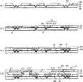
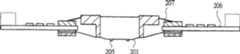
随着半导体元件的高密度化、窄间距化的发展,就需要进行高速信号的动作试验,作为在这种情况下能够进行半导体元件的特性检验的检验方法及检验装置,有1988年度的ITC(International TestConference;国际测试会议)的讲演论文集的第601页至第607页(非专利文献1)记载的技术。图27是该非专利文献所公开的检验装置的构造示意图,图28是该检验装置的关键部位放大立体图。在此所使用的半导体检验用的探针将如下结构作为接触端子使用,所述结构是这样形成的:在柔性的绝缘膜201的上表面以光刻技术形成配线202,在绝缘膜201的下表面形成接地层203,在与作为被检验对象的半导体的电极相对应的位置设置的绝缘膜201的通孔204处,通过电镀形成半球状的凸部205。该技术是下述这样的方法,即:使通过在绝缘膜201的表面形成的配线202及配线基板206而与检验电路(省略图示)连接的凸部205在板簧207的弹力的作用下擦过作为检验对象的半导体元件的电极而与之接触,从而来接收信号以进行检验。With the development of high-density and narrow-pitch semiconductor elements, it is necessary to perform high-speed signal operation tests. As an inspection method and inspection device that can perform characteristic inspections of semiconductor elements in this case, there is a 1988 ITC ( The technology described in the 601st to 607th pages (Non-Patent Document 1) of the lecture collection of the International TestConference (International TestConference). Fig. 27 is a schematic structural view of the inspection device disclosed in the non-patent document, and Fig. 28 is an enlarged perspective view of key parts of the inspection device. The semiconductor inspection probe used here uses the following structure as a contact terminal. The structure is formed by forming
另外,在日本特开平2-163664号公报(专利文献1)中,公开了半导体元件的检验装置,图29是该检验用探针卡的构造的示意图。它是如下构成的探针装置,即:将带有板簧207的枢轴销208保持在被旋转板209支承的圆锥井210中,以将凸部205及形成了配线的绝缘膜201推出。In addition, JP-A-2-163664 (Patent Document 1) discloses an inspection device for a semiconductor element, and FIG. 29 is a schematic view showing the structure of the inspection probe card. It is a probe device configured by holding a
另外,在日本特开2005-24377号公报(专利文献2)中,公开了半导体元件的检验装置,图30是该检验用探针卡的构造的示意图。它是如下这样的探针装置,即:将探针片分割成4份,通过设置在探针片中央的弹簧柱塞211,借助于推压隔片214以及缓冲部件将四棱锥状的接触端子212及形成了配线的绝缘膜213推出。In addition, JP-A-2005-24377 (Patent Document 2) discloses an inspection device for a semiconductor element, and FIG. 30 is a schematic view showing the structure of the inspection probe card. It is a probe device as follows, that is, the probe sheet is divided into four parts, and the contact terminal in the shape of a quadrangular pyramid is formed by pushing the
近年来,一直期望开发出使用能够在窄间距且多针的半导体元件的电极和检验电路之间传输电信号以进行动作检验的连接装置的半导体元件的检验装置。另外,对于高速电信号用半导体元件,为了降低介电损耗并进行微细配线,使用与二氧化硅(Sio2)相比介电常数小一些的材料(例如有机类材料)。由于这样的介电常数小的材料的耐负载以及机械强度都比较弱,所以为了不给该低介电材料带来损伤,期望检验装置能够以几10mN程度以下的低负载实现稳定的接触阻抗值。因此,从这样的观点出发对上述技术进行研究。In recent years, it has been desired to develop a semiconductor device inspection device using a connection device capable of transmitting electric signals between electrodes of a semiconductor device with narrow pitches and multiple pins and an inspection circuit for operation inspection. In addition, for semiconductor elements for high-speed electrical signals, materials with a lower dielectric constant than silicon dioxide (Sio2) (for example, organic materials) are used in order to reduce dielectric loss and perform fine wiring. Since the load resistance and mechanical strength of such a material with a small dielectric constant are relatively weak, in order not to damage the low dielectric material, it is desired that the inspection device can realize a stable contact resistance value with a low load of about several 10mN or less. . Therefore, the above-mentioned technique has been studied from such a viewpoint.
由钨针构成的探针以及形成了上述半球状的凸部的探针是,对于在铝电极或钎焊电极等的材料表面生成氧化物的被接触材料,通过将接触端子擦过电极来擦掉电极材料表面的氧化物,从而与其下面的金属导体材料接触,由此来确保接触状态。其结果是,由于用接触端子擦过电极而产生电极材料的碎屑,这导致配线间短路以及异物的产生。另外,由于探针以施加几百mN程度以上的负载的状态擦过电极来确保接触状态,所以有可能对低介电常数材料带来损伤。Probes made of tungsten needles and probes formed with the above-mentioned hemispherical protrusions are wiped by rubbing the contact terminal over the electrode for the material to be contacted that generates oxides on the surface of the material such as an aluminum electrode or a brazing electrode. Remove the oxide on the surface of the electrode material, so as to contact the metal conductor material below it, so as to ensure the contact state. As a result, debris of the electrode material is generated due to rubbing the electrode with the contact terminal, which leads to a short circuit between wirings and generation of foreign matter. In addition, since the probe rubs against the electrode with a load of about several hundred mN or more to ensure a contact state, there is a possibility of damaging the low dielectric constant material.
这样,如图27~图29所示,对于将在配线的局部上通过电镀而形成的凸部作为探针的方法,由于凸部的前端部是平坦或成为半球状,所以对于在铝电极或钎焊电极等的材料表面生成氧化物的被接触材料,不容易擦掉氧化物,所以接触阻抗变得不稳定,必须使接触时的负载为几百mN程度以上。但是,存在接触时的负载过大的问题。即,由于随着半导体元件的高集成化的发展,将高密度多针且窄间距的电极形成在半导体元件表面,所以大多在电极正下方形成大量有源元件或微细的配线,如果半导体元件检验时探针与电极的接触压力过大,则有可能对电极及其正下方的有源元件或配线带来损伤,因此需要在探测时特别注意动作控制,这会导致检验的处理量降低。In this way, as shown in FIGS. 27 to 29, in the method of using the protruding part formed by electroplating on a part of the wiring as a probe, since the tip of the protruding part is flat or hemispherical, it is difficult for the aluminum electrode For contact materials such as brazing electrodes where oxides are formed on the surface, it is difficult to wipe off the oxides, so the contact resistance becomes unstable, and the load at the time of contact must be more than several hundred mN. However, there is a problem that the load at the time of contact is too large. That is, since high-density multi-pin and narrow-pitch electrodes are formed on the surface of semiconductor elements with the development of high integration of semiconductor elements, a large number of active elements or fine wiring are often formed directly under the electrodes. If the contact pressure between the probe and the electrode is too high during inspection, it may cause damage to the electrode and the active components or wiring directly below it. Therefore, it is necessary to pay special attention to motion control during inspection, which will reduce the throughput of inspection. .
而且,由于预想到凸部的形状等会产生偏差,所以在使接触不充分的突起(凸部)完全接触时,整体需要更大的接触负载,从而存在局部的接触压力过大的问题。因此,除了需要贯通作为接触对象的材料表面的氧化物等而能确保稳定的接触特性的接触端子的形状,为了在探针片进行推压时能够可靠地与作为接触对象的电极接触,还需要具有柔软性的探针片。In addition, since variations in the shape of the protrusions are expected, when the insufficiently contacted protrusions (convexities) are completely brought into contact, a larger contact load is required as a whole, and there is a problem of excessive local contact pressure. Therefore, in addition to the shape of the contact terminal that can ensure stable contact characteristics through the oxide on the surface of the material to be contacted, in order to reliably contact the electrode to be contacted when the probe sheet is pressed, it is also necessary to Flexible probe sheet.
另外,在以窄间距配置的半导体元件的微小的检验用电极衬垫上,必须将检验用的接触端子以高位置精度进行接触,而且,在之后的工序中,为了防止在使用了该电极衬垫的引线接合或连接用凸部的形成时发生连接不良,就需要尽可能防止因探测导致电极衬垫面的粗糙。由此,要求探测痕尽可能地微小。In addition, on the microscopic electrode pads for inspection of semiconductor elements arranged at a narrow pitch, it is necessary to contact the contact terminals for inspection with high positional accuracy. In the event of poor connection during wire bonding of pads or formation of connecting protrusions, it is necessary to prevent as much as possible roughening of the electrode pad surface due to probing. Therefore, detection marks are required to be as small as possible.
对于使用图30所示的四棱锥状的接触端子,与半导体元件的检验用电极垂直地进行探测的检验装置,虽然接触阻抗值稳定,但在近年的寻求更窄间距化和高速的电信号检验的情况下,就更要求接触端子的前端位置精度的提高。而且,对于高速传输用电路形成材料,倾向于使用低介电常数的耐负载较弱的材料,因此为了防止在探测时对半导体元件的损伤,就需要更低负载的探针。For an inspection device that uses a rectangular pyramid-shaped contact terminal as shown in FIG. 30 and detects perpendicularly to the inspection electrode of a semiconductor element, although the contact resistance value is stable, in recent years, narrower pitches and high-speed electrical signal inspections have been sought. In the case of the contact terminal, it is more required to improve the positional accuracy of the tip of the contact terminal. In addition, for circuit formation materials for high-speed transmission, materials with low dielectric constant and weak load resistance tend to be used, so in order to prevent damage to semiconductor elements during probing, probes with lower loads are required.
发明内容Contents of the invention
本发明的目的是提供一种半导体装置检验用的探针卡,其能够在作为被接触对象的电极衬垫上以低负载而不带来损伤地进行探测检验,具有能够以多点且高密度且以小的探测痕进行接触的接触端子,并且传输特性良好,接触特性稳定。The object of the present invention is to provide a probe card for semiconductor device inspection, which can perform probing inspection with a low load on the electrode pad as the object to be contacted without causing damage, and has a multi-point and high-density probe card. Moreover, the contact terminal is contacted with a small detection mark, and the transmission characteristic is good, and the contact characteristic is stable.
另外,本发明提供一种探针卡,其能够将探测检验时的接触端子的前端位置精度保持为高精度。In addition, the present invention provides a probe card capable of maintaining the positional accuracy of the tip of the contact terminal at high precision during probing inspection.
另外,本发明提供一种采用了下述探针片的半导体装置检验用的探针卡,所述探针片实现了阻抗整合的高速传输用电路,使得高速传输信号的损失小。In addition, the present invention provides a probe card for semiconductor device inspection using a probe sheet that realizes impedance-integrated high-speed transmission circuits and reduces loss of high-speed transmission signals.
如下所述简单地说明本发明公开的发明中的有代表性的发明的概要。Outlines of typical inventions among the inventions disclosed in the present application will be briefly described as follows.
(1)本发明的探针卡具有探针片,该探针片包括:(1) The probe card of the present invention has a probe sheet, and the probe sheet includes:
与设置在被检验对象上的电极相接触的多个接触端子;a plurality of contact terminals in contact with electrodes provided on the object to be inspected;
从上述多个接触端子的各个端子引出的配线;Wiring drawn from each terminal of the above-mentioned plurality of contact terminals;
与上述配线电连接且与多层配线基板的电极连接的多个周边电极,a plurality of peripheral electrodes electrically connected to the wiring and connected to electrodes of the multilayer wiring board,
上述探针卡设有:以包围上述多个接触端子的方式形成的框;和The probe card is provided with: a frame formed to surround the plurality of contact terminals; and
对上述框施加推压力的多个机构。Multiple mechanisms that apply pushing force to the above frame.
(2)本发明的探针卡,是在上述(1)记载的探针卡中,设有使形成有上述框的区域内的形成有上述多个接触端子的区域可倾动的机构。(2) In the probe card of the present invention, in the probe card described in (1) above, there is provided a mechanism for tilting the area where the plurality of contact terminals are formed in the area where the frame is formed.
(3)本发明的探针卡具有探针片,该探针片包括:(3) The probe card of the present invention has a probe sheet, and the probe sheet includes:
与设置在被检验对象上的电极相接触的多个接触端子;a plurality of contact terminals in contact with electrodes provided on the object to be inspected;
从上述多个接触端子的各个端子引出的配线;Wiring drawn from each terminal of the above-mentioned plurality of contact terminals;
与上述配线电连接且与多层配线基板的电极连接的多个周边电极,a plurality of peripheral electrodes electrically connected to the wiring and connected to electrodes of the multilayer wiring board,
上述探针卡设有:以包围上述多个接触端子的方式形成的框;和使形成有上述框的区域内的形成有上述多个接触端子的区域可倾动的机构。The probe card includes: a frame formed to surround the plurality of contact terminals; and a mechanism for tilting an area in which the plurality of contact terminals is formed within an area in which the frame is formed.
(4)本发明的探针卡具有探针片,该探针片具有:(4) The probe card of the present invention has a probe sheet, and the probe sheet has:
与设置在被检验对象上的电极相接触的多个接触端子;a plurality of contact terminals in contact with electrodes provided on the object to be inspected;
从上述多个接触端子的各个端子引出的配线;Wiring drawn from each terminal of the above-mentioned plurality of contact terminals;
与上述配线电连接且与多层配线基板的电极连接的多个周边电极,a plurality of peripheral electrodes electrically connected to the wiring and connected to electrodes of the multilayer wiring board,
上述多个接触端子是棱锥形状或棱台形状,The above-mentioned plurality of contact terminals are pyramid-shaped or truncated-prism-shaped,
上述探针卡还设置有:将上述探针片的上述多个周边电极加压接触在上述多层配线基板的电极上的推压板;The probe card is further provided with: a pressing plate for pressure-contacting the plurality of peripheral electrodes of the probe sheet to the electrodes of the multilayer wiring board;
以包围上述多个接触端子的方式形成的框;和a frame formed in such a manner as to surround the plurality of contact terminals; and
对上述框施加推压力的多个机构,a plurality of mechanisms exerting a pushing force on the above-mentioned frame,
上述探针片以从上述多层配线基板伸出的方式被保持。The probe sheet is held so as to protrude from the multilayer wiring board.
(5)本发明的探针卡具有:(5) The probe card of the present invention has:
与用于检验被检验对象的电气特性的检验器电连接的多层配线基板;A multilayer wiring substrate electrically connected to a tester for testing electrical characteristics of an object to be tested;
探针片,具有与上述多层配线基板的电极连接的多个周边电极、以及与设置在上述被检验对象上的电极相接触的多个接触端子;A probe sheet having a plurality of peripheral electrodes connected to the electrodes of the multilayer wiring board, and a plurality of contact terminals in contact with the electrodes provided on the object to be inspected;
以包围上述多个接触端子的方式形成的框;a frame formed in such a manner as to surround the plurality of contact terminals;
对上述框施加推压力的多个机构,a plurality of mechanisms exerting a pushing force on the above-mentioned frame,
上述多个接触端子是棱锥形状或棱台形状,The above-mentioned plurality of contact terminals are pyramid-shaped or truncated-prism-shaped,
上述施加推压力的多个机构被配置成使得形成有上述框的区域和形成有上述多个接触端子的区域可倾动。The plurality of mechanisms for applying the pressing force are arranged so that the region where the frame is formed and the region where the plurality of contact terminals are formed are tiltable.
(6)本发明的探针卡,是在上述(1)~(5)任一项所述的探针卡中,上述探针片具有与上述配线电连接的地线层以及电源配线层中的至少一层,(6) The probe card of the present invention is the probe card described in any one of (1) to (5) above, wherein the probe sheet has a ground layer electrically connected to the wiring and a power supply wiring. at least one of the layers,
与上述地线层或上述电源配线层连接的配线被形成得配线宽度比与上述地线层和上述电源配线层中的任意一个都不连接的配线的配线宽度宽。The wiring connected to the ground layer or the power wiring layer is formed to have a wider wiring width than the wiring not connected to either the ground layer or the power wiring layer.
(7)本发明的探针卡,是上述(1)~(6)中任一项所述的探针卡中,在探针片中央设有施加推压力的机构。(7) The probe card of the present invention is the probe card described in any one of (1) to (6) above, wherein a mechanism for applying a pressing force is provided at the center of the probe sheet.
(8)本发明的探针卡,是上述(1)~(6)中任一项所述的探针卡中,向上述框施加推压力的上述多个机构是多个具有弹性的导销。(8) In the probe card of the present invention, in the probe card described in any one of (1) to (6) above, the plurality of mechanisms for applying a pressing force to the frame are a plurality of elastic guide pins. .
(9)本发明的探针卡,是上述(1)~(6)中任一项所述的探针卡中,向上述框施加推压力的上述多个机构包括:多个具有弹性的导销;和多个没有弹性的导销。(9) In the probe card of the present invention, in the probe card described in any one of (1) to (6), the plurality of mechanisms for applying a pressing force to the frame include: a plurality of elastic guides; pin; and a plurality of inelastic guide pins.
(10)本发明的探针卡,是上述(1)~(9)中任一项所述的探针卡中,上述多个接触端子是以通过对具有结晶性的基板进行异方性蚀刻而形成的孔为型材通过电镀来形成的。(10) The probe card of the present invention is the probe card described in any one of the above (1) to (9), wherein the plurality of contact terminals are obtained by performing anisotropic etching on a crystalline substrate. The holes formed are formed by electroplating on the profile.
(11)本发明的半导体检验装置具有:(11) The semiconductor inspection device of the present invention has:
承载被检验对象的试料台;和a test stand carrying the object to be tested; and
具有与设于上述被检验对象上的电极相接触的多个接触端子,且与用于检验上述被检验对象的电气特性的检验器电连接的探针卡;a probe card having a plurality of contact terminals in contact with electrodes provided on the object to be inspected and electrically connected to a tester for inspecting the electrical characteristics of the object to be inspected;
上述探针卡具有探针片,该探针片具有:The above probe card has a probe sheet with:
与设置在上述被检验对象上的电极相接触的上述多个接触端子;the above-mentioned plurality of contact terminals in contact with the electrodes provided on the above-mentioned inspected object;
从上述多个接触端子的各个端子引出的配线;和Wiring drawn from each of the above-mentioned plurality of contact terminals; and
与上述配线电连接且与多层配线基板的电极连接的多个周边电极,a plurality of peripheral electrodes electrically connected to the wiring and connected to electrodes of the multilayer wiring board,
上述探针卡设有以包围上述多个接触端子的方式形成的框;The probe card is provided with a frame formed to surround the plurality of contact terminals;
对上述框施加推压力的多个机构;和a plurality of mechanisms that apply pushing force to the frame; and
使形成有上述框的区域内的形成有上述多个接触端子的区域可倾动的机构。A mechanism for tilting the area where the plurality of contact terminals are formed within the area where the frame is formed.
(12)本发明的半导体检验装置具有:(12) The semiconductor inspection device of the present invention has:
承载被检验对象的试料台;和a test stand carrying the object to be tested; and
具有与设于上述被检验对象上的电极相接触的多个接触端子,且与用于检验上述被检验对象的电气特性的检验器电连接的探针卡;a probe card having a plurality of contact terminals in contact with electrodes provided on the object to be inspected and electrically connected to a tester for inspecting the electrical characteristics of the object to be inspected;
上述探针卡具有探针片,该探针片具有:The above probe card has a probe sheet with:
与设置在上述被检验对象上的电极相接触的上述多个接触端子;the above-mentioned plurality of contact terminals in contact with the electrodes provided on the above-mentioned inspected object;
从上述多个接触端子的各个端子引出的配线;和Wiring drawn from each of the above-mentioned plurality of contact terminals; and
与上述配线电连接且与多层配线基板的电极连接的多个周边电极,a plurality of peripheral electrodes electrically connected to the wiring and connected to electrodes of the multilayer wiring board,
上述多个接触端子是棱锥形状或棱台形状,The above-mentioned plurality of contact terminals are pyramid-shaped or truncated-prism-shaped,
上述探针卡还设置有:将上述探针片的上述多个周边电极加压接触在上述多层配线基板的电极上的推压板;The probe card is further provided with: a pressing plate for pressure-contacting the plurality of peripheral electrodes of the probe sheet to the electrodes of the multilayer wiring board;
以包围上述多个接触端子的方式形成的框;和a frame formed in such a manner as to surround the plurality of contact terminals; and
对上述框施加推压力的多个机构,a plurality of mechanisms exerting a pushing force on the above-mentioned frame,
上述探针片以从上述多层配线基板伸出的方式被保持。The probe sheet is held so as to protrude from the multilayer wiring board.
(13)本发明的半导体检验装置具有:(13) The semiconductor inspection device of the present invention has:
承载被检验对象的试料台;和a test stand carrying the object to be tested; and
具有与设于上述被检验对象上的电极相接触的多个接触端子,且与用于检验上述被检验对象的电气特性的检验器电连接的探针卡;a probe card having a plurality of contact terminals in contact with electrodes provided on the object to be inspected and electrically connected to a tester for inspecting the electrical characteristics of the object to be inspected;
上述探针卡具有:The above probe card has:
与用于检验被检验对象的电气特性的检验器电连接的多层配线基板;A multilayer wiring substrate electrically connected to a tester for testing electrical characteristics of an object to be tested;
探针片,具有与上述多层配线基板的电极连接的多个周边电极、以及与设置在上述被检验对象上的电极相接触的多个接触端子;A probe sheet having a plurality of peripheral electrodes connected to the electrodes of the multilayer wiring board, and a plurality of contact terminals in contact with the electrodes provided on the object to be inspected;
以包围上述多个接触端子的方式形成的框;a frame formed in such a manner as to surround the plurality of contact terminals;
对上述框施加推压力的多个机构,a plurality of mechanisms exerting a pushing force on the above-mentioned frame,
上述多个接触端子是棱锥形状或棱台形状,The above-mentioned plurality of contact terminals are pyramid-shaped or truncated-prism-shaped,
上述施加推压力的多个机构被配置成使得形成有上述框的区域和形成有上述多个接触端子的区域可倾动。The plurality of mechanisms for applying the pressing force are arranged so that the region where the frame is formed and the region where the plurality of contact terminals are formed are tiltable.
(14)本发明的半导体装置的制造方法,具有以下工序:(14) The manufacturing method of the semiconductor device of the present invention has the following steps:
向半导体晶片中植入电路以及与上述电路电连接的电极以形成多个半导体元件的工序;The process of implanting circuits and electrodes electrically connected to the circuits in a semiconductor wafer to form a plurality of semiconductor elements;
利用探针卡对上述多个半导体元件的电气特性进行检验的工序,上述探针卡具有与设于上述多个半导体元件上的上述电极相接触的多个接触端子,且与对形成在上述多个半导体元件的各个半导体元件上的上述电路的电气特性进行检验的检验器电连接;和The process of inspecting the electrical characteristics of the plurality of semiconductor elements using a probe card, the probe card having a plurality of contact terminals in contact with the electrodes provided on the plurality of semiconductor elements, and connected to the plurality of contact terminals formed on the plurality of semiconductor elements The tester is electrically connected to the tester for testing the electrical characteristics of the above-mentioned circuit on each of the semiconductor components; and
对上述半导体晶片进行切割,并按上述多个半导体元件的每一个进行分离的工序;A process of dicing the above-mentioned semiconductor wafer and separating each of the above-mentioned plurality of semiconductor elements;
上述探针卡具有探针片,该探针片具有:The above probe card has a probe sheet with:
与设置在上述多个半导体元件上的电极相接触的上述多个接触端子;said plurality of contact terminals in contact with electrodes provided on said plurality of semiconductor elements;
从上述接触端子的各个端子引出的配线;和Wiring from each of the above-mentioned contact terminals; and
与上述配线电连接且与多层配线基板的电极连接的多个周边电极,a plurality of peripheral electrodes electrically connected to the wiring and connected to electrodes of the multilayer wiring board,
上述多个接触端子是棱锥形状或棱台形状,The above-mentioned plurality of contact terminals are pyramid-shaped or truncated-prism-shaped,
上述探针卡还设置有:以包围上述多个接触端子的方式形成的框;和对上述框施加推压力的多个机构,The probe card is further provided with: a frame formed to surround the plurality of contact terminals; and a plurality of mechanisms for applying a pressing force to the frame,
施加上述推压力的上述多个机构被配置成使得形成有上述框的区域和形成有上述多个接触端子的区域可倾动,The plurality of mechanisms for applying the pressing force are configured so that the region where the frame is formed and the region where the plurality of contact terminals are formed are tiltable,
上述探针卡通过上述框对以从上述多层配线基板伸出的方式被保持的上述探针片的形成有上述多个接触端子的上述区域施加推压力,并且使上述多个接触端子与设于上述半导体元件上的上述电极接触来检验上述电路的上述电气特性。The probe card applies a pressing force to the region in which the plurality of contact terminals are formed on the probe sheet held so as to protrude from the multilayer wiring board through the aforementioned frame, and makes the plurality of contact terminals and The above-mentioned electrode provided on the above-mentioned semiconductor element is contacted to test the above-mentioned electrical characteristics of the above-mentioned circuit.
(15)本发明的半导体装置的制造方法,是在上述(14)所述的半导体装置的制造方法中,上述多个接触端子是以通过对具有结晶性的基板进行异方性蚀刻而形成的孔为型材通过电镀来形成的。(15) In the method for manufacturing a semiconductor device of the present invention, in the method for manufacturing a semiconductor device described in (14) above, the plurality of contact terminals are formed by anisotropic etching of a crystalline substrate. The holes are formed by electroplating in the profile.
本发明的上述及其他的目的、特征以及优点在以下的更详细的用于实施本发明的最佳实施方式的描述以及附图中明示。The above and other objects, features, and advantages of the present invention are shown in the following more detailed description of the best mode for carrying out the present invention and the accompanying drawings.
附图说明Description of drawings
图1是表示配列了半导体元件(芯片)的被接触对象即晶片及一部分的半导体元件(芯片)的立体图。FIG. 1 is a perspective view showing a wafer, which is an object to be contacted, on which semiconductor elements (chips) are arranged, and a part of the semiconductor elements (chips).
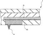
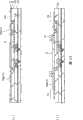
图2是本发明的实施方式1的探针卡的关键部位剖视图。2 is a sectional view of essential parts of the probe card according to Embodiment 1 of the present invention.
图3是图2所示的探针卡的主要部件的分解立体图。FIG. 3 is an exploded perspective view of main components of the probe card shown in FIG. 2 .
图4是分解图2所示的探针卡的主要部件进行图示的组装剖视图。FIG. 4 is an assembled cross-sectional view showing main parts of the probe card shown in FIG. 2 in disassembled view.
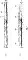
图5是表示图2所示的探针卡的主要部件即导销的关键部位的剖视图。FIG. 5 is a sectional view showing essential parts of a guide pin which is a main part of the probe card shown in FIG. 2 .
图6是本发明的实施方式1的探针卡的关键部位剖视图。6 is a sectional view of essential parts of the probe card according to Embodiment 1 of the present invention.
图7是本发明的实施方式2的探针卡的关键部位剖视图。7 is a sectional view of essential parts of a probe card according to
图8是本发明的实施方式3的探针卡的关键部位剖视图。8 is a sectional view of essential parts of a probe card according to
图9是本发明的实施方式3的探针卡的接触端子组附近的放大的关键部位剖视图。FIG. 9 is an enlarged cross-sectional view of key parts in the vicinity of a contact terminal group of a probe card according to
图10是本发明的实施方式4的探针卡的关键部位剖视图。10 is a sectional view of essential parts of a probe card according to
图11是本发明的实施方式5的探针卡的关键部位剖视图。11 is a sectional view of essential parts of a probe card according to
图12是图11所示的探针卡的主要部件的分解立体图。Fig. 12 is an exploded perspective view of main components of the probe card shown in Fig. 11 .
图13是本发明的实施方式6的探针卡的关键部位剖视图。13 is a sectional view of essential parts of a probe card according to
图14是本发明的实施方式7的探针卡的关键部位剖视图。14 is a sectional view of essential parts of a probe card according to
图15是本发明的实施方式8的探针卡的关键部位剖视图。15 is a sectional view of essential parts of a probe card according to
图16是本发明的实施方式9的探针卡的关键部位剖视图。16 is a sectional view of essential parts of a probe card according to
图17是本发明的实施方式10的探针卡的关键部位剖视图。17 is a sectional view of essential parts of the probe card according to
图18是本发明的实施方式11的探针卡的关键部位剖视图。18 is a sectional view of essential parts of the probe card according to
图19是本发明的实施方式12的探针卡的关键部位剖视图。19 is a sectional view of essential parts of a probe card according to
图20(a)~图20(f)是表示本发明的实施方式13的探针卡中的形成探针片(探针片构造体)部分的制造流程的一部分的关键部位剖视图。FIGS. 20( a ) to 20 ( f ) are cross-sectional views showing a part of the manufacturing process of the portion where the probe sheet (probe sheet structure) is formed in the probe card according to
图21(g)~图21(i)是表示图20的后续制造流程的关键部位剖视图。21(g) to 21(i) are cross-sectional views of key parts showing the subsequent manufacturing process of FIG. 20 .
图22(a)~图22(d)是表示本发明的实施方式14的探针卡中的形成探针片(探针片构造体)部分的制造流程的一部分的关键部位剖视图。FIGS. 22( a ) to 22 ( d ) are cross-sectional views of key parts showing a part of the manufacturing flow of the portion where the probe sheet (probe sheet structure) is formed in the probe card according to
图23(a)以及图23(b)是表示本发明的实施方式15的探针卡中的形成探针片(探针片构造体)部分的制造流程的一部分的关键部位剖视图。23( a ) and FIG. 23( b ) are cross-sectional views of key parts showing a part of the manufacturing flow of the portion where the probe sheet (probe sheet structure) is formed in the probe card according to
图24(a)以及图24(b)是表示本发明的实施方式16的探针卡中的形成探针片(探针片构造体)部分的制造流程的一部分的关键部位剖视图。24( a ) and FIG. 24( b ) are cross-sectional views of key parts showing a part of the manufacturing flow of the part where the probe sheet (probe sheet structure) is formed in the probe card according to
图25是表示本发明的实施方式17的检验系统的一例的整体示意结构图。25 is an overall schematic configuration diagram showing an example of an inspection system according to
图26是表示半导体装置的检验工序的一例的工序图。FIG. 26 is a process diagram showing an example of an inspection process of a semiconductor device.
图27是使用了现有电镀形成的凸部的半导体元件检验装置的关键部位剖视图。Fig. 27 is a cross-sectional view of key parts of a semiconductor device inspection device using conventional plating-formed protrusions.
图28是表示图27的电镀形成的凸部部分的立体图。FIG. 28 is a perspective view showing a convex portion formed by plating in FIG. 27 .
图29是使用了现有电镀形成的凸部的半导体元件检验装置的关键部位剖视图。Fig. 29 is a cross-sectional view of key parts of a semiconductor element inspection device using conventional plating-formed protrusions.
图30是使用了形成有四棱锥接触端子的现有探针片的半导体元件检验装置的关键部位剖视图。30 is a cross-sectional view of key parts of a semiconductor element inspection device using a conventional probe sheet on which contact terminals of rectangular pyramids are formed.
具体实施方式Detailed ways
在以下的实施方式中,为了方便,在必要时分割成多个部分或实施方式进行说明,但是,除特别明示的情况以外,它们之间并不是毫无关系的,一个实施方式是另一实施方式的一部分或全部的变形例、是详细、补充说明等的关系。In the following embodiments, for convenience, they are divided into a plurality of parts or embodiments for description as necessary. However, unless otherwise specified, there is no relationship between them, and one embodiment is another embodiment. Modifications of some or all of the embodiments are related to details, supplementary explanations, and the like.
另外,在以下的实施方式中,涉及到要素的数量(包含个数、数值、量、范围等)的情况下,除特别明示的情况以及原理上明确限定为特定数量的情况等以外,不限于其特定数量,可以是特定数量以上也可以是特定数量以下。In addition, in the following embodiments, when referring to the number of elements (including numbers, numerical values, amounts, ranges, etc.), it is not limited to, except for the case where it is specifically stated and the case where it is clearly limited to a specific number in principle. The specific number may be more than or less than the specific number.
而且,在以下的实施方式中,其结构要素(也包含要素步骤等)除特别明示的情况以及原理上明确是必须的情况等以外,不一定是必须的。另外,在实施例等中,关于结构要素等,说“由A构成”、“由A形成”时,除特别地明确只有该要素的情况等以外,不能排除除此以外的要素。In addition, in the following embodiments, the constituent elements (including elemental steps, etc.) are not necessarily essential, except for cases where they are particularly clearly stated and are clearly essential in principle. In addition, in the examples and the like, when "consisting of A" or "formed of A" is used for structural elements, other elements cannot be excluded unless it is specifically specified that only the element is present.
同样地,在以下的实施方式中,涉及到构成要素等的形状、位置关系等时,除特别明示的情况以及原理上明确地不成立的情况等以外,还包含实质上与其形状等近似或类似的要素等。关于这一点,上述数值以及范围也是一样的。Similarly, in the following embodiments, when referring to the shape, positional relationship, etc. of components, etc., except for the case where it is specifically stated and the case where it is clearly not established in principle, it also includes those that are substantially similar to or similar to the shape, etc. elements etc. In this regard, the above-mentioned numerical value and range are also the same.
另外,涉及到材料等时,除特别指明不是的情况或者在原理上或按情况不是的情况以外,特定的材料为主要材料,并不排除次要的要素、添加物、附加要素等。例如,硅部件除特别明示的情况等,不仅是纯硅的情况,还可以是以添加不纯物、硅为主要要素的二元、三元等的合金(例如SiGe)等。In addition, when it comes to materials, etc., unless otherwise specified or in principle or circumstances, a specific material is the main material, and secondary elements, additives, additional elements, etc. are not excluded. For example, the silicon member is not limited to pure silicon, but may include binary, ternary, or other alloys (such as SiGe) with additives and silicon as main components, unless otherwise specified.
另外,在用于说明本实施方式的所有附图中,具有相同功能的要素原则上使用相同的附图标记,并省略对其重复说明。In addition, in all the drawings for describing the present embodiment, elements having the same function are assigned the same reference numerals in principle, and repeated description thereof will be omitted.
另外,在本实施方式所使用的附图中,在俯视图中,也有为了容易理解附图而部分地使用了剖面线的情况。In addition, in the drawings used in this embodiment, hatching may be partially used in plan view to facilitate understanding of the drawings.
在以下的实施方式以及实施例中,主要用语如下定义。In the following embodiments and examples, main terms are defined as follows.
所谓半导体装置,与其形态无关,可以是形成有电路的晶片状态的装置,也可以是半导体元件,还可以是之后封装而成的装置(QFP(Quad Flat Package;四侧引脚扁平封装)、BGA(Ball Grid Array;球栅阵列封装)以及CSP(Chip Size Package;芯片尺寸封装)等)。The so-called semiconductor device, regardless of its form, may be a device in the form of a chip with a circuit formed thereon, or a semiconductor element, or a device that is packaged later (QFP (Quad Flat Package), BGA (Ball Grid Array; ball grid array package) and CSP (Chip Size Package; chip size package) etc.).
所谓探针片,是指设有与检验对象接触的接触端子和从那里引回的配线且在该配线上形成了外部连接用的电极的薄膜,其以厚度为10μm~100μm左右的薄膜为对象。The so-called probe sheet refers to a thin film with a contact terminal in contact with the test object and a wiring drawn from there, and an electrode for external connection is formed on the wiring. It is a thin film with a thickness of about 10 μm to 100 μm. for the object.
所谓探针卡是表示具有与检验对象接触的端子、多层配线基板等的构造体(例如,后述实施方式中用图2说明的构造体)。The term "probe card" refers to a structure (for example, a structure described with reference to FIG. 2 in the embodiment described later) having a terminal in contact with an inspection object, a multilayer wiring board, and the like.
所谓半导体检验装置是表示具有承载探针卡和检验对象的试料支承系统的检验装置。The term "semiconductor inspection device" refers to an inspection device having a sample support system on which a probe card and an inspection object are placed.
如图1所示,作为被检验对象的一例的LSI用半导体元件(芯片)2在晶片1上形成多个,之后被切开以供使用。图1是表示并列设置有多个LSI用半导体元件2的晶片1的立体图,放大其一部即1个半导体元件2进行表示。在半导体元件2的表面上,沿着周边排列有与形成在半导体元件2内的电路电连接的多个电极3。As shown in FIG. 1 , a plurality of LSI semiconductor elements (chips) 2 , which are an example of inspection targets, are formed on a wafer 1 and then cut out for use. FIG. 1 is a perspective view showing a wafer 1 on which a plurality of
然而,在半导体元件2中,随着高集成化,上述电极3的配置的高密度化以及窄间距化处于进一步发展的状况。电极3的配置的窄间距化的倾向趋向0.1mm程度以下,例如,逐渐成为0.08mm、0.04mm或更小。作为电极3的高密度化的倾向,有沿着半导体元件2的周边从1列到两列进而在整个面上排列的倾向。However, in the
另外,还有实施高温动作试验(85℃~150℃)的倾向,即:通过在高温下对半导体元件进行动作试验来更明确地掌握半导体元件的特性以及可靠性。In addition, there is a tendency to conduct a high-temperature operation test (85° C. to 150° C.), that is, to more clearly grasp the characteristics and reliability of the semiconductor element by performing an operation test on the semiconductor element at a high temperature.
以下实施例的半导体检验装置能与上述电极3的高密度化以及窄间距化相对应且能够进行基于高速电信号(100MHz~20GHz)的检验。The semiconductor inspection apparatus of the following examples can cope with the increase in density and narrow pitch of the
另外,作为半导体检验装置中的探针卡的一部分的构成材料,使用具有150℃的耐热性,且线膨胀率与被检验对象相同的材料,由此能够防止因环境温度引起的探针前端部的位置偏移。In addition, as a part of the constituent material of the probe card in the semiconductor inspection device, a material having a heat resistance of 150°C and having the same linear expansion coefficient as the object to be inspected can prevent the tip of the probe from being damaged due to the ambient temperature. position offset.
以下,利用图2~图19对本实施方式的半导体装置检验用探针卡进行说明。Hereinafter, the probe card for semiconductor device inspection according to this embodiment will be described with reference to FIGS. 2 to 19 .
(实施方式1)(Embodiment 1)
图2是表示本实施方式1的探针卡的关键部位的剖视图,图3是图2所示的主要部件的分解立体图,图4是分解图2所示的主要部件进行图示的组装剖视图。利用图2~图5对本实施方式1的探针卡进行说明。2 is a cross-sectional view showing essential parts of the probe card according to Embodiment 1, FIG. 3 is an exploded perspective view of main components shown in FIG. 2 , and FIG. 4 is an assembled cross-sectional view illustrating the main components shown in FIG. The probe card according to Embodiment 1 will be described with reference to FIGS. 2 to 5 .
本实施方式1的探针卡由弹簧柱塞4、框5、中间板6以及多个导销7等构成。The probe card according to Embodiment 1 is composed of a
弹簧柱塞(向探针片中央施加推压力的机构)4以在高度方向上可调整的状态固定在中间板6的中央部,并且在该弹簧柱塞4的下部前端具有突起部4a,以起中央枢轴的作用,该弹簧柱塞4装填有弹簧4b,该弹簧4b以该突起部4a的前端为支点通过可动的推压隔片8对探针片9施加推压力。A spring plunger (mechanism for applying a pressing force to the center of the probe sheet) 4 is fixed to the central portion of the
框5被粘接固定在探针片9的内表面,并包围探针片9的形成有接触端子10组的区域。The
在中间板6和探针片9的形成有接触端子10组的区域的内表面之间,在中央部具有硅片等缓冲部件11及推压隔片8,并且,中间板6螺纹固定在上述框5上。Between the
导销7被插入在支承部件(上部固定板)12中并被螺纹固定在上述中间板6上。另外,为了极力防止在探测检验时接触端子前端的位置偏移,并且为了以在形成有接触端子10组的区域微倾的状态下可进行动作(微倾动)的状态实现所期望的大致恒定的推压力(例如,在500针左右的的情况下,推入量为150μm左右,推压力为5~10N左右),使用内置有图5所示的弹簧13的弹簧内置导销7a以及定位专用导销7b构成导销7。这些多个弹簧内置导销(对框施加推压力的多个机构)7a以及多个定位专用导销7b被插入在支承部件7中,并被螺纹固定在中间板6上进行使用。另外,弹簧内置导销7a具有以下构造:在金属制的管7c内内置上述弹簧13及中轴7d,通过弹簧13的弹性力使中轴7d推压中间板6;定位专用导销7b具有以下构造:在金属制的管7c内内置中轴7e,通过将中轴7e固定在中间板6上来进行定位。导销7至少设置3根,优选设置4根以上。另外,为了防止接触端子前端的位置偏移,优选在支承部件12中,使供导销7插入的插入孔12a和插入后的导销7之间尽量没有间隙(游隙),在本实施方式1中,以插入孔12a的直径比导销7的直径仅大10μm~20μm左右为例。The
推压隔片8是被保持成通过在中间板6的中央部设置的弹簧柱塞4的前端的突起部4a可微倾动,并通过该弹簧柱塞4施加(推压)所期望的大致恒定的推压力的构造的随动机构。并且,在推压隔片8的上表面中央部形成有与突起部4a卡合的圆锥槽8a。The
并且,弹簧柱塞4也可以省去弹簧4b并以突起部4a为支点在可微倾动的状态下使用(参照图10),其详细说明将在后面描述。Furthermore, the
在上述探针片9中,在片的探测(主面)侧的中央区域部形成有用于与半导体元件2的电极3组接触的上述接触端子10组,并以二重包围该接触端子10组的周围的方式形成金属膜14a和位于与框5对应的区域的金属膜14b。另外,在探针片9的4边的周边部,形成有用于与多层配线基板15进行信号的收发的、具有与上述接触端子10组相同构造的周边电极16组,以包围该周边电极16组的方式在与周边电极固定板17对应的区域形成金属膜14c。并且,周边电极16组具有与上述接触端子10组相同的构造,前端与多层配线基板15的电极15b连接。另外,在接触端子10组和周边电极16组之间,形成有图3所示的多个引出配线18。用于形成接触端子10组以及周边电极16组的各接触端子是棱锥形状或棱台形状,其详细说明将在后面描述。In the above-mentioned
另外,在探针片9的形成有上述接触端子10组的区域的内表面粘接固定有上述框5,在探针片9的形成有用于信号收发的上述周边电极16组的部分的内表面粘接固定有上述周边电极固定板17。In addition, the above-mentioned
而且,上述框5被螺纹固定在螺纹固定有多个导销7的中间板6上。在该中间板6上固定有弹簧柱塞4,下部前端的突起部4a与在推压隔片8的上表面中央形成的圆锥槽8a卡合。Further, the above-mentioned
在金属膜14c上通过蚀刻预先形成定位用的定位销用孔14e和螺栓插入用孔14f的布图,在周边电极固定板17以及周边推压板20上也分别预先形成定位用的定位销用孔17e、20e以及螺栓插入用孔17f、20f,由此能够提高组装性。The layout of positioning pin holes 14e for positioning and
隔着缓冲部件19将周边推压板20螺纹固定在以包围周边电极16组的方式固定于探针片9上的周边电极固定板17上,由此隔着缓冲部件19使周边电极16组与多层配线基板15的电极15b连接。The peripheral
另外,也可以使用在支承部件12上设置的倾斜微调用双螺栓21或者间隔片22a(参照图6)来对形成有接触端子10组的区域的探针片9的倾斜进行微调整。在此,双螺栓21是在外侧的螺栓21a的中央形成了另外一个中间螺栓21b而成的部件,是通过用外侧的螺栓21a调整支承部件12与上板22的间隔来微调整两者的倾斜,然后用中间螺栓21b进行螺纹固定的构造。In addition, the inclination of the
另外,在探针片9中形成有与基准电位(接地电位)电连接的地线23。通过将这样的地线23设置在探针片9中,能够防止在探测检验时所传输的信号波形的紊乱。In addition, a
另外,在探针片9的内表面安装有芯片电容器24。该芯片电容器24通过形成在探针片9中的配线而与接触端子10组中的规定的接触端子电连接。这样的芯片电容器24的配置在通过将芯片电容器24配置在接触端子10的附近来极力防止信号的紊乱的情况下起作用。In addition, a
由上述各种部件形成本实施方式1的探针片构造体25。The
根据上述本实施方式1,由于是在用多个导销7(具有弹性的弹簧内置导销7a、定位专用导销7b)定位探针片9的同时施加推压力的结构,所以能够实现将推压负载控制在宽范围内的窄间距多针的半导体检验用探针卡。随着半导体元件2内的高集成化发展,为了将高密度多针且窄间距的电极3形成在半导体元件2的表面上,大多在电极3的正下方形成有多个有源元件或微细的配线,若在对半导体元件2检验时接触端子10组对电极3组的接触压力过大,则有可能对电极3及其正下方的有源元件或配线产生损伤,但在本实施方式1的半导体检验用探针卡中,由于能够将推压负载控制在宽范围内,所以能够防止对有源元件或配线的损伤。According to the first embodiment described above, since the plurality of guide pins 7 (elastic spring built-in
另外,也预想到了半导体元件2的表面的电极3组的面和接触端子10组的面发生倾斜的情况。此时,根据上述本实施方式1,图2中由单点划线包围的区域内的弹簧柱塞4、框5、中间板6、导销7、推压隔片8、探针片9、缓冲部件11以及金属膜14a、14b,在形成有接触端子10组的区域可微倾动的状况下,能够进行推压动作。由此,不需要用于使接触不充分的接触端子和电极3完全接触的更大的接触负载,因此能够防止接触端子10组和电极3组之间的接触压力局部过大,同时还能够使接触端子10组和接触对象的电极3组可靠地接触。其结果,能够尽可能地防止因探测导致的电极3的表面的粗糙,因此即使在低负载下也能确保稳定的接触特性即稳定的接触阻抗值。In addition, it is also conceivable that the surfaces of the
(实施方式2)(Embodiment 2)
图7是表示本实施方式2的探针卡的关键部位的剖视图。在上述实施方式1中,表示了在探针片9上形成地线23并搭载芯片电容器24的情况(参照图2以及图6),但在不需要高速电检验信号的情况下,如图7所示,也可以是省略地线23或芯片电容器24或者两者都省略的结构。FIG. 7 is a cross-sectional view showing essential parts of the probe card according to
在以下说明的探针卡的结构中,根据检验信号的速度,也可以是同样地省略地线23或芯片电容24的结构。另外,倾斜微调节用双螺栓21(参照图2)或间隔片22a(参照图6)可以根据需要使用,也可以省略。In the structure of the probe card described below, depending on the speed of the test signal, the
另外,在上述实施方式1所示的图2中,表示了以二重包围接触端子10组的周围的方式形成金属膜14a以及位于与框5对应的区域的金属膜14b的例子,但如图7所示,可以根据所需要的接触端子的前端位置精度省略金属膜14a或金属膜14b中的一方,或是两方都省略。In addition, in FIG. 2 shown in Embodiment 1 above, an example in which the
在探针片9中形成的配线(配线材料)中,与基准电位(接地电位)电连接的上述地线23以及与电源电连接的配线也可以形成为比不与基准电位(接地电位)或电源电连接的其他配线尽可能宽的配线宽度。由此,通过地线23以及与电源电连接的配线,能够使配线阻抗值降低,从而能够极力防止探测检验时的电压变动。In the wiring (wiring material) formed on the
根据具有上述构造的本实施方式2的探针片构造体25b,也能够得到与上述实施方式1相同的效果。Also according to the probe sheet structure 25b of the second embodiment having the above-mentioned structure, the same effect as that of the first embodiment described above can be obtained.
(实施方式3)(Embodiment 3)
图8是表示本实施方式3的探针卡的关键部位的剖视图,图9是本实施方式3的探针卡的接触端子10附近的放大的关键部位剖视图。使用图8以及图9对本实施方式3的探针卡进行说明。8 is a cross-sectional view showing essential parts of the probe card according to the third embodiment, and FIG. 9 is an enlarged cross-sectional view showing the main parts near the
在探针片9中,在形成有各个接触端子10的连接电极部10b和配线材料26连接的情况下,在上述实施方式1中是通过通孔,但是在本实施方式3中省略通孔而直接在连接电极部10b的表面上形成配线材料26(参照图9)。其他结构与上述实施方式1相同。In the
根据具有上述构造的本实施方式3的探针片构造体25c,由于是省略了上述通孔的构造,所以能够降低连接电极部10b和配线材料26之间的接触阻抗值。另外,在制造探针片9的工序中,由于能够省略制造上述通孔的工序,所以能够缩短探针片9的制造的TAT(TurnAround Time;周转时间)。而且,由于能够省略用于形成通孔的掩模,所以能够降低探针片9的制造成本。According to the
通过具有上述构造的本实施方式3的探针片构造体25c,也能够得到与上述实施方式1相同的效果。Also with the
(实施方式4)(Embodiment 4)
图10是表示本实施方式4的探针卡的关键部位的剖视图。使用图10对本实施方式4的探针卡进行说明。FIG. 10 is a cross-sectional view showing essential parts of a probe card according to
本实施方式4的探针卡由支承部件12、导销7、中间板6c以及框5等构成。The probe card according to
导销7如上述实施方式1中使用图2进行说明那样,被插入在支承部件12中并被螺纹固定在上述中间板6c上。The
中间板6c具有突起部27a及调整螺栓27b。突起部27a以在探针片9的伸出方向上可调整的方式被固定在该中间板6c的中央部,以起中央枢轴的作用;调整螺栓27b以该突起部27a的前端为支点,通过可动的推压隔片8将探针片9调整到所期望的伸出量。The
框5如上述实施方式1使用图2进行说明的那样,被粘接固定在探针片9的内表面,并包围探针片9的形成有接触端子10组的区域。
在探针片9的形成有接触端子10组的区域的内表面和中间板6c之间,硅片等缓冲部件11以及推压隔片8被配置在中央部,中间板6c被螺纹固定在框5上。Between the inner surface of the area where the
在此,在本实施方式4的探针卡中,推压隔片8被保持成通过设置在中间板6c的中央部的突起部27a可微倾动,另外,在中间板6c上具备如下构造的随动机构,即:被保持成通过螺纹固定在中间板6c上的多个弹簧内置导销7a(参照图5)以及多个定位专用导销7b(参照图5)可微倾动,并且施加所期望的大致恒定的推压力(推压)。这样的本实施方式4的探针卡使接触端子10组以低负载在接近平行的状态下对半导体元件2等的电极3组开始加压,从而能够可靠地进行接触端子10组的随动动作,进而能够防止接触端子以及半导体元件2等的电极3的损伤。Here, in the probe card according to
由上述各种部件形成本实施方式4的探针片构造体25d。The
通过具有上述构造的本实施方式4的探针片构造体25d,也能够得到与上述实施方式1相同的效果。Also with the
(实施方式5)(Embodiment 5)
图11是表示本实施方式5的探针卡的关键部位的剖视图,图12是图11所示的主要部件的分解立体图。使用图11以及图12对本实施方式5的探针卡进行说明。FIG. 11 is a sectional view showing essential parts of the probe card according to
本实施方式5的探针卡由弹簧柱塞4、框5b、中间板6b以及导销7等构成。The probe card according to
弹簧柱塞4以在高度方向上可调整的状态被固定在中间板6b的中央部,并在下部前端具有突起部4a,以起中央枢轴的作用,在弹簧柱塞4中装填有以该突起部4a的前端为支点通过可动的推压隔片8对探针片9施加推压力的弹簧4b。The
框5b被粘接固定在探针片9c的内表面,并包围探针片9c的形成有接触端子10组的区域。The
在探针片9c的形成有接触端子10组的区域的内表面和中间板6b之间,硅片等缓冲部件11以及推压隔片8被配置在中央部,中间板6b被螺纹固定在框5b上。Between the inner surface of the region where the
导销7被插入在支承部件(上部固定板)12b中并被螺纹固定在上述中间板6b上。另外,导销7如上述实施方式中说明的那样,是为了极力防止在探测检验时接触端子前端的位置偏移,并且为了以在形成有接触端子10组的区域微倾的状态下可动作(微倾动)的状态实现所期望的大致恒定的推压力(例如,在500针左右的的情况下,推入量为150μm左右,推压力为5~10N左右),使用内置有图5所示的弹簧13的弹簧内置导销7a以及定位专用导销7b的结构。这些多个弹簧内置导销7a以及多个定位专用导销7b被插入在支承部件12b中,并被螺纹固定在中间板6b上。The
上述探针片9c在片的探测(主面)侧的中央区域部形成有用于与半导体元件2的电极3组接触的接触端子10组,并且以二重包围该接触端子10组的周围的方式形成金属膜14a及位于与框5b对应的区域的金属膜14b。另外,在探针片9c的周边部形成有用于与多层配线基板15a进行信号收发的周边电极16a组,在接触端子10组和周边电极16a组之间形成有多个引出配线18a。在探针片9c的内表面,隔着与周边电极16a组的内表面相对设置的O型环30将O型推压环31螺纹固定在多层配线基板15a上,由此能够通过O型环30将周边电极16a组连接到多层配线基板15a的电极15c上。The above-mentioned
而且,在探针片9c的形成有上述接触端子10组的区域的内表面粘接固定上述框5b,框5b被螺纹固定在中间板6b上。在该中间板6b上固定有弹簧柱塞4,下部前端的突起部4a与形成在推压隔片8的上表面中央的圆锥槽8a卡合。另外,在中间板6b上螺纹固定有被插入在支承部件12b中的导销7。Furthermore, the
推压隔片8是被保持成通过设置在中间板6的中央部的弹簧柱塞4的前端的突起部4a可微倾动,并通过该弹簧柱塞4施加(推压)所期望的大致恒定的推压力的构造的随动机构。并且,在推压隔片8的上表面中央部形成有与突起部4a卡合的圆锥槽8a。The
并且,如后述的图17~图19所示,弹簧柱塞4可以是省略了弹簧4b的构造,在以突起部4a为支点可微倾动的状态下使用。In addition, as shown in FIGS. 17 to 19 described later, the
并且,可以使用设置在支承部件12b上的倾斜微调用双螺栓21或间隔片(间隔片22a(参照图6))来对探针片9c的形成有接触端子10组的区域的倾斜进行微调整。在此,双螺栓21是在外侧的螺栓21a的中央形成另外一个中螺栓21b而成的部件,具有通过用外侧的螺栓21a调整支承部件12b和上板22b的间隔来对两者的倾斜进行微调整,然后用中螺栓21b进行螺纹固定的构造。In addition, the inclination of the region of the
由上述各种部件构成本实施方式5的探针片构造体25e。The
通过具有上述构造的本实施方式5的探针片构造体25e,也能得到与上述实施方式1相同的效果。Also with the
(实施方式6)(Embodiment 6)
图13是表示本实施方式6的探针卡的关键部位的剖视图。使用图13对本实施方式6的探针卡进行说明。FIG. 13 is a cross-sectional view showing essential parts of a probe card according to
在上述实施方式5(参照图11以及图12)中,表示了在探针片9c上形成地线23c并搭载芯片电容器24的情况,但是在并不那样需要高速电检验信号的情况下,如本实施方式6即图13所示,也可以是在探针片9d中省略地线23c或芯片电容器24的结构。In Embodiment 5 (see FIGS. 11 and 12 ), the case where the
在以下说明的探针卡的结构中,也可以是根据检验信号的速度同样地省略地线23c或芯片电容器24的结构。另外,倾斜微调节用的双螺栓21或间隔片22a根据需要使用即可,当然也可以省略。In the structure of the probe card described below, the
另外,在上述实施方式5的图11中,表示了以二重包围接触端子10组的周围的方式形成金属膜14a以及位于与框5b对应的区域的金属膜14b的例子,但如本实施方式6的图13所示,可以根据所需要的接触端子的前端位置精度省略金属膜14a或金属膜14b,或者两者都省略。In addition, in FIG. 11 of the above-mentioned fifth embodiment, an example in which the
由上述各种部件构成本实施方式6的探针片构造体25f。The
通过具有上述构造的本实施方式6的探针片构造体25f,也能得到与上述实施方式1相同的效果。Also with the
(实施方式7)(Embodiment 7)
图14是表示本实施方式7的探针卡的关键部位的剖视图。使用图14对本实施方式7的探针卡进行说明。FIG. 14 is a cross-sectional view showing essential parts of a probe card according to
在形成有接触端子10的连接电极部10b和上层的配线材料连接的情况下,在上述实施方式5中是通过通孔连接,但在本实施方式7中则是与上述实施方式3(参照图8以及图9)同样,省略通孔直接在连接电极部10b的表面形成配线材料26b。其他结构与上述实施方式5相同。In the case where the
由上述各种部件构成本实施方式7的探针片构造体25g。The
通过具有上述构造的本实施方式7的探针片构造体25g,也能够得到与上述实施方式1相同的效果。Also with the
(实施方式8)(Embodiment 8)
图15是表示本实施方式8的探针卡的关键部位的剖视图。使用图15对本实施方式8的探针卡进行说明。FIG. 15 is a cross-sectional view showing essential parts of a probe card according to
在本实施方式8中,代替上述实施方式5的探针卡(参照图10)中的被螺纹固定在中间板6c上的导销7,使用固定在弹簧柱塞保持部件32上的弹簧柱塞32a的构造的随动推压机构。In the eighth embodiment, instead of the
即,本实施方式8的探针卡具有支承部件12c、弹簧柱塞保持部件32、弹簧柱塞32a、弹簧柱塞4、框5c、缓冲部件11以及推压隔片8等。That is, the probe card according to the eighth embodiment includes the supporting
弹簧柱塞保持部件32被螺纹固定在支承部件12c上,弹簧柱塞32a被装填到弹簧柱塞保持部件32上。The spring
弹簧柱塞4以在高度方向上可调整的状态被固定在中间板6c的中央部,在下部前端具有突起部4a,以起中央枢轴的作用,该弹簧柱塞4装填有以该突起部4a的前端为支点通过可动的推压隔片8对探针片9c施加推压力的弹簧4b。The
框5c被粘接固定在探针片9c的内表面,并包围探针片9c的形成有接触端子10组的区域。The
在探针片9c的形成有接触端子10组的区域的内表面和中间板6c之间,硅片等缓冲部件11以及推压隔片8被配置在中央部,中间板6c被螺纹被固定在框5c上。Between the inner surface of the region where the
在本实施方式8的探针卡中具有如下构造的随动机构,即:推压隔片8被保持成通过设置在中间板6c的中央部的弹簧柱塞4的前端的突起部4a可微倾动,并且中间板6c被保持成通过被装填在弹簧柱塞保持部件32上的多个弹簧柱塞32a可微倾动,由此施加(推压)所期望的大致恒定的推压力。本实施方式8的探针卡使接触端子10组以低负载在接近平行的状态下对半导体元件2等的电极3组开始加压,从而可靠地进行接触端子10组的随动动作,进而能够防止接触端子以及半导体元件2等的电极3的损伤。In the probe card according to the eighth embodiment, there is a following mechanism in which the
由上述各种部件构成本实施方式8的探针片构造体25h。The
通过具有上述构造的本实施方式8的探针片构造体25h,也能得到与上述实施方式1相同的效果。Also with the
(实施方式9)(Embodiment 9)
图16是表示本实施方式9的探针卡的关键部位的剖视图。使用图16对本实施方式9的探针卡进行说明。FIG. 16 is a cross-sectional view showing essential parts of a probe card according to
在本实施方式9中,代替上述实施方式8的探针卡中的被弹簧柱塞保持部件32保持的弹簧柱塞32a,具有使用了被弹簧保持部件33保持的弹簧33a的构造的随动推压机构。其他结构与上述实施方式8相同。In this ninth embodiment, instead of the
由上述各种部件构成本实施方式9的探针片构造体25i。The probe sheet structure 25i of the ninth embodiment is constituted by the various components described above.
通过具有上述构造的本实施方式9的探针片构造体25i,也能得到与上述实施方式1相同的效果。Also with the probe sheet structure 25i of the ninth embodiment having the above-mentioned structure, the same effect as that of the first embodiment described above can be obtained.
(实施方式10)(Embodiment 10)
图17是表示本实施方式10的探针卡的关键部位的剖视图。使用图17对本实施方式10的探针卡进行说明。FIG. 17 is a cross-sectional view showing essential parts of the probe card according to the tenth embodiment. A probe card according to
本实施方式10的探针卡是具有支承部件12b、导销7、中间板6e以及框5b等的构造。The probe card according to
导销7被插入在支承部件12b中并螺纹固定在中间板6e上。The
中间板6e具有突起部27a以及调整螺栓27b。突起部27a以在探针片9的伸出方向上可调整的方式被固定在该中间板6e的中央部,以起中央枢轴的作用;调整螺栓27b以该突起部27a的前端为支点通过可动的推压隔片8将探针片9调整成所期望的伸出量。The intermediate plate 6e has a
框5b被粘接固定在探针片9c的内表面,并包围探针片9c的形成有接触端子10组的区域。The
在探针片9c的形成有接触端子10组的区域的内表面和中间板6e之间,硅片等缓冲部件11以及推压隔片8被配置在中央部,中间板6e被螺纹固定在框5b上。Between the inner surface of the region where the
在此,在本实施方式10的探针卡中,推压隔片8被保持成通过设置在中间板6e的中央部的突起部27a可微倾动,另外,在中间板6e上具备如下构造的随动机构,即:被保持成通过螺纹固定在中间板6e上的多个弹簧内置导销7a(参照图5)以及多个定位专用导销7b(参照图5)可微倾动,并且施加(推压)所期望的大致恒定的推压力。本实施方式10的探针卡使接触端子10组以低负载在接近平行的状态下对半导体元件2等的电极3组开始加压,从而能够可靠地进行接触端子10组的随动动作,进而能够防止接触端子以及半导体元件2等的电极3的损伤。Here, in the probe card according to the tenth embodiment, the
由上述各种部件构成本实施方式10的探针片构造体25j。The
根据具有上述构造的本实施方式10的探针片构造体25j,也能得到与上述实施方式1相同的效果。Also according to the
(实施方式11)(Embodiment 11)
图18是表示本实施方式11的探针卡的关键部位的剖视图。使用图18对本实施方式11的探针卡进行说明。FIG. 18 is a cross-sectional view showing essential parts of the probe card according to the eleventh embodiment. A probe card according to
在本实施方式11中,代替上述实施方式10的探针卡(参照图17)中的被螺纹固定在中间板6e上的导销7,构成采用了固定在弹簧柱塞保持部件32上的弹簧柱塞32a的构造的随动推压机构。另外,中间板6f被螺纹固定在框5c上。其他结构与上述实施方式10相同。In the eleventh embodiment, instead of the
由上述各种部件构成本实施方式11的探针片构造体25k。The
通过具有上述构造的本实施方式11的探针片构造体25k,也能得到与上述实施方式1相同的效果。Also with the
(实施方式12)(Embodiment 12)
图19是表示本实施方式12的探针卡的关键部位的剖视图。使用图19对本实施方式12的探针卡进行说明。FIG. 19 is a cross-sectional view showing essential parts of the probe card according to the twelfth embodiment. A probe card according to
在本实施方式12中,代替上述实施方式10的探针卡(参照图17)中的被螺纹固定在中间板6e上的多个导销7,构成采用了被装填到弹簧保持部件33中的多个弹簧33a的构造的随动推压机构。其他结构与上述实施方式10相同。In the twelfth embodiment, instead of the plurality of
由上述各种部件构成本实施方式12的探针片构造体251。The
通过具有上述构造的本实施方式12的探针片构造体251,也能得到与上述实施方式1相同的效果。The
以下,对与实施本发明的最佳方式对应的实施例进行说明。Examples corresponding to the best mode for carrying out the present invention will be described below.
(实施方式13)(Embodiment 13)
接下来,关于在上述实施方式1~12中说明的探针卡中使用的探针片(探针片构造体)的一例,参照图20说明其制造方法。另外,形成以下的探针片的各部件在图2~图19所示的上述实施方式1~12的探针卡的关键部位剖视图中也有适当表示。Next, an example of the probe sheet (probe sheet structure) used in the probe cards described in Embodiments 1 to 12 will be described with reference to FIG. 20 . In addition, each member forming the following probe sheet is also appropriately shown in the sectional views of key parts of the probe card according to the above-mentioned Embodiments 1 to 12 shown in FIGS. 2 to 19 .
图20以及图21按照工序顺序示出了用于形成上述实施方式1中图2所示的探针卡的制造流程中的制造工序,尤其是下述的制造工序:在作为型材的硅晶片40上以异方性蚀刻形成棱台形状的孔40a,将该孔40a作为型材使用,使棱台形状的接触端子部41以及引出配线用的配线材料26一体地形成在聚酰亚胺膜42上,再在其表面形成聚酰亚胺膜43以及配线材料26c,然后用粘结层52接合金属膜14,在该金属膜14形成固定着框5的探针片9。20 and 21 show the manufacturing steps in the manufacturing flow for forming the probe card shown in FIG. Form a prism-shaped
首先,实施图20(a)所示的工序。该工序是在厚度0.2~0.6mm的硅晶片40的(100)面的两面通过热氧化形成0.5μm左右的二氧化硅膜44,然后涂布光致抗蚀剂,通过光刻工序形成除去了开有棱台形状的孔的位置的光致抗蚀剂的图案。接着,将该光致抗蚀剂作为掩模,用氢氟酸和氟化铵的混合液蚀刻除去二氧化硅膜44,将上述二氧化硅膜44作为掩模,用强碱液(例如,氢氧化钾)异方性蚀刻硅晶片40,以形成棱台形状的孔40a。First, the steps shown in Fig. 20(a) are carried out. In this process, a
在此,在本实施方式13中是将硅晶片40作为型材,但是,作为型材,只要是具有结晶性的材料即可,在该范围内当然可以进行各种变更。另外,在本实施方式13中,通过异方性蚀刻形成的孔是棱台形状,但是该形状也可以是棱锥状,在能够形成能确保小的针压且稳定的接触阻抗的程度的接触端子10组的形状的范围内,可以进行各种变更。另外,在作为接触对象的1个电极上也可以用多个接触端子接触。Here, in the thirteenth embodiment, the
接下来,实施图20(b)所示的工序。在该工序中,用氢氟酸和氟化铵的混合液蚀刻除去作为掩模使用的二氧化硅膜44,然后再次通过在湿氧中的热氧化,在硅晶片40的整个表面上形成0.5μm左右的二氧化硅膜45。接下来,实施以下工序:在该二氧化硅膜45的表面形成导电性覆膜46,然后在该导电性覆膜46的表面形成光致抗蚀剂掩模47,并使得连接端子部41开口。Next, the process shown in FIG. 20(b) is carried out. In this process, the
接下来,实施图20(c)所示的工序。在该工序中,将上述光致抗蚀剂掩模47作为掩模,将上述导电性覆膜46作为供电层,以硬度高的材料为主要成分进行电镀,从而将接触端子10和连接电极部10b形成为一体。此时,还形成了与接触端子10相同构造的周边电极16。之后,实施除去光致抗蚀剂掩模47的工序。作为硬度高的电镀材料,例如依次电镀镍41a、铑41b以及镍41c,只要使接触端子10及连接电极部10b成为一体形成接触端子部41即可。Next, the process shown in FIG. 20(c) is implemented. In this step, the above-mentioned
接下来,实施图20(d)所示的工序。该工序是,形成聚酰亚胺膜42,以覆盖上述接触端子部41以及导电性覆膜46,然后将位于应形成从上述接触端子部41引出的引出配线连接用孔的位置的聚酰亚胺膜42除去,直至到达上述接触端子部41的表面,在该聚酰亚胺膜42上形成导电性覆膜48,形成光致抗蚀剂掩模49,然后电镀配线材料26。Next, the process shown in FIG. 20(d) is carried out. This step is to form a
在除去上述聚酰亚胺膜42的一部分时,使用例如激光开孔加工或以形成在聚酰亚胺膜42的表面上的铝掩模为掩模的干蚀刻即可。When part of the
作为上述导电性覆膜48,例如将铬通过溅射法或蒸镀法成膜,由此形成厚度0.1μm左右的铬膜,在形成了该铬膜的表面上将铜通过溅射法或蒸镀法成膜,由此形成厚度1μm左右的铜膜即可。另外,作为配线材料26,使用实施了镀铜或在镀铜上实施了镀镍的材料即可。As the above-mentioned
接下来,实施图20(e)所示的工序。该工序是,除去上述光致抗蚀剂掩模49,将配线材料26作为掩模,将导电性覆膜48软蚀刻除去,然后形成聚酰亚胺膜43,将位于应形成从配线材料26与上部的配线材料26c连接用的孔的位置的聚酰亚胺膜43除去,直至到达上述配线材料26的表面。接着,在聚酰亚胺膜43上形成导电性覆膜50,形成光致抗蚀剂掩模51,之后电镀配线材料26c。Next, the process shown in FIG. 20(e) is carried out. This step is to remove the above-mentioned
在除去上述聚酰亚胺膜43的一部分时,与聚酰亚胺膜42的情况相同,使用例如激光开孔加工或以形成在聚酰亚胺膜43的表面上的铝掩模为掩模的干蚀刻即可。When removing a part of the
作为上述导电性覆膜50,与导电性覆膜48同样地,例如将铬通过溅射法或蒸镀法成膜,由此形成厚度0.1μm左右的铬膜,在形成了该铬膜的表面上将铜通过溅射法或蒸镀法成膜,由此形成厚度1μm左右的铜膜即可。另外,作为配线材料26c,与配线材料26同样地使用实施了镀铜或在镀铜上实施了镀镍的材料即可。As the above-mentioned
接下来,实施图20(f)所示的工序。该工序是,除去上述光致抗蚀剂掩模51,将配线材料26c作为掩模将导电性覆膜50软蚀刻除去,之后将粘结层52以及金属膜14粘结在聚酰亚胺膜43以及配线材料26c上,利用光致抗蚀剂掩模蚀刻该金属膜14,以形成所期望的金属膜14的图案(金属膜14a~14c)。Next, the process shown in FIG. 20(f) is carried out. In this step, the
在此,作为粘结层52,使用例如聚酰亚胺类粘结片或环氧类粘结片即可。另外,作为金属膜14,使用具有42合金(镍42%以及铁58%的合金,线膨胀率为4ppm/℃)或不胀钢(例如,镍36%以及铁64%的合金,线膨胀率为1.5ppm/℃)那样的线膨胀率且线膨胀率与硅晶片(硅型材)40的线膨胀率接近的金属片,使该金属片通过粘结层52粘贴在形成了配线材料26c的聚酰亚胺膜43上,由此能够实现所形成的探针片9的强度的提高以及大面积化,还能防止检验时因温度导致的位置偏移等,从而能够确保在各种状况下的位置精度。在该主旨中,作为金属膜14,以确保预烧检验时的位置精度为目的,也可以使用具有与作为检验对象的半导体元件2的线膨胀率接近的线膨胀率的材料。Here, as the
上述粘结工序可以是,例如使形成有接触端子部41、配线材料26以及聚酰亚胺膜43的硅晶片40、与粘结层52以及金属膜14重合,以10~200kgf/cm2左右加压并施加粘结层52的玻璃转移点温度(Tg)以上的温度,在真空中加热加压粘结。The above-mentioned bonding process can be, for example, making the
另外,作为金属膜14的产生图案用的光致抗蚀剂掩模,可以用液状保护膜也可以用膜状保护膜(干膜)。In addition, as a photoresist mask for patterning the
接下来,实施图21(g)所示的工序。该工序是后续工序(参照图21(h))的预处理,首先,用保护膜覆盖形成有金属膜14的面,以中央被挖通的保护膜作为掩模,用氢氟酸和氟化铵的混合液将从相反面的硅蚀刻用保护夹具的盖53b(参照图21(h))露出的区域的二氧化硅膜45蚀刻除去。接着,剥离该保护膜,然后将硅蚀刻用保持环54用粘结剂55粘结在上述聚酰亚胺膜52上。此外,作为金属膜14,在使用42合金片或不胀钢片的情况下,用氯化亚铁溶液喷雾蚀刻即可。Next, the process shown in FIG. 21(g) is implemented. This process is the pretreatment of the subsequent process (refer to Figure 21 (h)). First, cover the surface on which the
接下来,实施图21(h)所示的工序。该工序是,将硅蚀刻用保护夹具安装在硅晶片40上,将硅蚀刻除去。Next, the process shown in FIG. 21(h) is implemented. In this step, the protective jig for silicon etching is mounted on the
例如,在中间固定板56d上螺纹固定上述硅蚀刻用保持环54,将隔着O型环53c安装在不锈钢制的固定夹具53a和不锈钢制的盖53b之间的作为型材的硅晶片40用强碱液(例如,氢氧化钾)蚀刻除去即可。For example, the above-mentioned
接下来,实施图21(i)所示的工序。该工序是,拆除上述硅蚀刻用保护夹具,将保护膜以覆盖单面的方式粘结在硅蚀刻用保持环54上,然后蚀刻除去二氧化硅膜45、导电性覆膜46(铬以及铜)以及镍41a。接着,除去该保护膜,然后在金属膜14与探针片的框5以及周边电极固定板17之间涂布粘结剂55b,以固定在金属膜14的规定位置。Next, the process shown in FIG. 21(i) is carried out. This step is to remove the above-mentioned protective jig for silicon etching, bond the protective film to the holding
二氧化硅膜45用氢氟酸和氟化铵的混合液蚀刻除去,铬膜用过锰酸钾液蚀刻除去,铜膜以及镍膜41a用碱性铜蚀刻液蚀刻除去即可。The
另外,这一系列蚀刻处理的结果是,使用从接触端子表面露出的铑41b,这是因为其难以附着作为半导体元件2的电极3的材料的钎焊、铝等,并且比镍的硬度高,难以被氧化,接触阻抗稳定。In addition, as a result of this series of etching processes, rhodium 41b exposed from the surface of the contact terminal is used because it is difficult to adhere to brazing, aluminum, etc. Difficult to be oxidized, stable contact resistance.
然后,沿着上述框5以及周边电极固定板17的外周部,切下聚酰亚胺膜42、43以及粘结层52,制成使用了导销7的探针片构造体25(参照图2)。Then, the
另外,将沿着组装工序用保持环的外周部切下的探针片9组装到探针卡上的工序的说明图用图3的立体图、图4的剖视图表示。In addition, explanatory views of the process of assembling the
当将探针片9组装到探针卡上时,由于是探针片9的周边电极16的前端与多层配线基板15的电极15b接触的结构,所以周边电极16和电极15b的接触稳定,能够容易地得到探测检验时的电气特性。When the
(实施方式14)(Embodiment 14)
接下来,参照图22对与上述实施方式13中说明的探针片9的制造工序有若干不同的本实施方式14的探针片的制造方法进行说明。Next, a method of manufacturing a probe sheet according to
图22(a)~图22(d)按工序顺序示出与上述实施方式13有若干不同的形成探针片9(参照实施方式3以及图8)的制造流程。FIGS. 22( a ) to 22 ( d ) show the manufacturing flow for forming the probe sheet 9 (refer to
在将形成有接触端子10的连接电极部10b与配线材料26连接的情况下,在实施方式13中是通过通孔连接,但在本实施方式14的制造工序中,没有形成通孔而是直接在连接电极部10b的表面形成配线材料26。其他结构与上述实施方式13相同。In the case of connecting the
首先,经过与上述实施方式13中的图20(a)、图20(b)相同的工序,在图22(a)所示的硅晶片40上形成棱锥状的蚀刻孔40a,然后在该表面形成二氧化硅膜45,在形成于该二氧化硅膜45上的导电性覆膜46的表面上形成聚酰亚胺膜42b。接着,实施将位于应形成接触端子10的位置的聚酰亚胺膜42b除去直至到达上述导电性覆膜46的表面的工序。First, a pyramid-shaped
作为上述导电性膜46,例如,将铬通过溅射法或蒸镀法成膜,由此形成厚度0.1μm左右的铬膜,在形成了该铬膜的表面上将铜通过溅射法或蒸镀法成膜,形成厚度1μm左右的铜膜即可。也可以在该铜膜上电镀几μm厚的铜,以增加激光加工的耐性。As the above-mentioned
在除去上述聚酰亚胺膜42b的一部分时,例如使用激光开孔加工或将形成在聚酰亚胺膜42b表面上的铝掩模作为掩模的干蚀刻即可。When removing part of the
接下来,实施图22(b)所示的工序。首先,对从上述聚酰亚胺膜42b的开口部露出的导电性覆膜46,以该导电性膜46为电极,以硬度高的材料为主要成分进行电镀,从而将接触端子10和连接电极部10b形成为一体。作为硬度高的电镀材料,例如依次电镀镍41a、铑41b、镍41c,使接触端子10和连接电极部10b作为一体形成接触端子部41即可。另外,此时,还形成与接触端子10相同构造的周边电极16。Next, the process shown in FIG. 22(b) is carried out. First, the
接下来,实施图22(c)所示的工序。首先,在上述接触端子部41以及聚酰亚胺膜42b上形成导电性覆膜48b,接着在形成了光致抗蚀剂掩模49b之后镀配线材料26。Next, the process shown in FIG. 22(c) is carried out. First, the
作为上述导电性膜48b,例如将铬通过溅射法或蒸镀法成膜,由此形成厚度0.1μm左右的铬膜,在形成了该铬膜的表面上将铜通过溅射法或蒸镀法成膜,由此形成厚度1μm左右的铜膜即可。另外,作为配线材料26,使用铜即可。As the above-mentioned
接着,实施图22(d)所示的工序。该工序是,除去上述光致抗蚀剂掩模49b,以配线材料26作为掩模软蚀刻除去导电性覆膜48b,然后形成聚酰亚胺膜43,将位于应形成从配线材料26与上部的配线材料26d连接用的孔的位置的聚酰亚胺膜43除去,直至到达上述配线材料26的表面。接着,在聚酰亚胺膜43上形成导电性覆膜50b,并在形成了光致抗蚀剂掩模之后,镀配线材料26d。Next, the process shown in FIG. 22(d) is implemented. This step is to remove the photoresist mask 49b, remove the
接着,除去该光致抗蚀剂掩模,以配线材料26d作为掩模软蚀刻除去导电性覆膜50b,之后粘结粘结层52以及金属膜14,利用光致抗蚀剂掩模蚀刻该金属膜14以形成所期望的金属膜14的图案(金属膜14a~14c)。Next, the photoresist mask is removed, and the
在除去上述聚酰亚胺膜43的一部分时,使用例如激光开孔加工或以形成在聚酰亚胺膜43表面上的铝掩模为掩模的干蚀刻即可。When part of the
作为上述导电性覆膜50b,与导电性覆膜48b同样地,例如将铬通过溅射法或蒸镀法成膜,由此形成厚度0.1μm左右的铬膜,在形成了该铬膜的表面上将铜通过溅射法或蒸镀法成膜,由此形成厚度1μm左右的铜膜即可。另外,作为配线材料26d,与配线材料26同样地使用实施了镀铜或在镀铜上实施了镀镍的材料即可。As the above-mentioned
接下来,经过与上述实施方式13中使用图20(g)~图21(i)说明的工序相同的工序,制成本实施方式14的探针片构造体25c(参照图8)。Next, the
(实施方式15)(Embodiment 15)
下面,就本实施方式15的探针片的制造方法,参照图23说明其制造工序。Next, the manufacturing process of the probe sheet of the fifteenth embodiment will be described with reference to FIG. 23 .
本实施方式15的探针片的制造方法,除了为了使探针片9c(参照上述实施方式5以及图11)的周边电极16a与多层配线基板15a的电极15c接触而将周边电极16a形成在整个接触端子10的形成面的相反面上的工序这点以外,其他与上述实施方式13(参照图20以及图21)所述的探针片9的制造方法相同。In the method of manufacturing a probe sheet according to
本实施方式15的探针片的制造方法是,首先,经过与上述实施方式13中使用图20(a)~图20(e)说明的工序相同的工序,形成聚酰亚胺膜42c、43c、配线材料26以及导电性覆膜50等,进一步,在这些各部件上形成了光致抗蚀剂掩模51,然后镀配线材料26d。配线材料26d的一部分成为与规定的接触端子10电连接的地线23c,配线材料26d的另一部分成为用于搭载芯片电容器24的电容器连接用电极57(参照图23(a))。In the method of manufacturing the probe sheet according to the fifteenth embodiment, first, the
如上述实施方式1中说明的那样,配线材料26d中的与基准电位(接地电位)电连接的上述地线23c以及与电源电连接的配线在探测检验时流过比其他配线大的电流。因此,这些地线23以及与电源电连接的配线以比其他配线材料26d宽的配线宽度形成,以便使配线阻抗降低。As described in Embodiment 1, the above-mentioned
接下来,实施图23(b)所示的工序。该工序是,除去上述光致抗蚀剂掩模51,将配线材料26d作为掩模软蚀刻除去导电性覆膜50,然后在使作为配线材料26d一部分的周边电极16a的部分露出的状态下以覆盖配线材料26d以及聚酰亚胺膜43c的方式粘结连接层52以及金属膜14。接着,将光致抗蚀剂掩模作为掩模蚀刻该金属膜14以形成所期望的金属膜14的图案(金属膜14a,14b(参照图11))。Next, the process shown in FIG. 23(b) is carried out. In this step, the
接下来,经过与上述实施方式13中使用图20(g)~图21(i)说明的工序相同的工序,制成使用了图11所示的导销7的探针片构造体25e。Next, the
另外,为了实现高速传输信号的稳定化,也可以根据需要在作为电容器连接用电极57的配线材料26d和地线23c用的配线材料26d的配线间设置芯片电容器24。In addition, in order to stabilize the high-speed transmission signal,
(实施方式16)(Embodiment 16)
下面,就本实施方式16的探针片的制造方法,参照图24说明其制造工序。Next, the manufacturing process of the probe sheet of the sixteenth embodiment will be described with reference to FIG. 24 .
本实施方式16的探针片的制造方法,与上述实施方式15的探针片9c的制造方法同样,为了使探针片9d(参照上述实施方式6以及图13)的周边电极16a与多层配线基板15a的电极15c接触而将周边电极16a形成在整个接触端子10的形成面的相反面。而且是具有将探针片9d中的配线材料即信号配线和电源配线形成在同一个面上的探针片构造的情况的制造方法。The method of manufacturing the probe sheet in the sixteenth embodiment is the same as the method for manufacturing the
首先,实施图24(a)所示的工序。在该工序中,首先,经过与上述实施方式13中使用图20(a)~图20(d)说明的工序相同的工序,形成导电性覆膜46、聚酰亚胺膜42以及导电性覆膜48d等,进一步,在这些部件上形成了光致抗蚀剂掩模49d之后,镀配线材料26e。First, the steps shown in Fig. 24(a) are carried out. In this process, first, the
接下来,实施图24(b)所示的工序。该工序是,除去上述光致抗蚀剂掩模49d,将配线材料26e作为掩模软蚀刻除去导电性覆膜48d,然后在使周边电极16a的部分露出的状态下以覆盖配线材料26e以及聚酰亚胺膜42的方式形成聚酰亚胺膜43d。Next, the process shown in FIG. 24(b) is carried out. In this step, the
接下来,经过与上述实施方式13中使用图20(g)~图21(i)说明的工序相同的工序,制成使用了图13所示的导销7的探针片构造体25f。Next, the
(实施方式17)(Embodiment 17)
下面,利用图25对使用了上述实施方式1~12说明的探针卡(探测装置)的半导体检验装置进行说明。Next, a semiconductor inspection device using the probe card (probing device) described in Embodiments 1 to 12 above will be described with reference to FIG. 25 .
图25是表示包括本实施方式17的半导体检验装置的检验系统的整体概略结构的图,示出了将所期望的负载施加在晶片1的面上以实施电特性检验的试验装置。在该状态下,导销的推压力(负载)施加在所有接触端子10上,通过与晶片1的电极3接触的接触端子10、引出配线18(配线材料26)、周边电极16、多层配线基板15的电极15b、内部配线15d以及电极15e,在对植入晶片1中的半导体元件2(省略在图25中的符号)进行电气特性检验的检验器58和半导体元件2之间实施检验用电信号的收发。25 is a diagram showing an overall schematic configuration of an inspection system including a semiconductor inspection apparatus according to
在检验系统的整体结构中,探针卡作为晶片探针构成。该检验系统由以下部件构成:支承作为被检验对象的晶片1的试料支承系统59;与被检验对象(晶片1)的电极3接触以进行电信号的收发的探针卡60;控制试料支承系统59的动作的驱动控制系统61;进行被检验对象(晶片1)的温度控制的温度控制系统62;和进行半导体元件(芯片)2的电气特性的检验的检验器58。在该晶片1上排列有前述多个半导体元件(芯片)2,在各半导体元件2的表面上排列有作为外部连接电极的多个电极3。试料支承系统59由以下部件构成:将晶片1可拆装地载置的、大致水平设置的试料台63;以支承该试料台63的方式垂直配置的升降轴64;对该升降轴64进行升降驱动的升降驱动部65;支承该升降驱动部65的X-Y平台66。X-Y平台66被固定在筐体67的上方。升降驱动部65例如由步进电动机等构成。试料台63的在水平以及垂直方向上的定位动作是通过将在X-Y平台66的水平面内的移动动作和升降驱动部65的上下动作等组合而进行的。另外,在试料台63上设置有未图示的转动机构,从而试料台63能够在水平面内进行转动移位。In the overall structure of the inspection system, the probe card is configured as a wafer probe. The inspection system is composed of the following components: a
在试料台63的上方配置有探针卡60。即,例如,图25所示的探针卡60以与对应的试料台63上平行相对的姿态设置。各接触端子10借助设置在探针卡60的探针片9上的引出配线18以及周边电极16,通过多层配线基板15的电极15b以及内部配线15d与设置在该多层配线基板15上的电极15e电连接,并通过与该电极15e连接的电缆68而与检验器58电连接。The
驱动控制系统61通过电缆69与检验器58电连接。另外,驱动控制系统61将控制信号送到试料支承系统58的各驱动部的致动器,以控制其动作。即,驱动控制系统61在内部具有计算机,其结合通过电缆69传输来的检验器58的检验动作的进行信息来控制试料支承系统59的动作。另外,驱动控制系统61具有操作部70,以接受与驱动控制相关的各种指令的输入,例如接受手动操作的指令。The
在试料台63上具有用于加热晶片1(半导体元件2)的加热器71。温度控制系统62通过控制试料台63的加热器71或冷却夹具来控制搭载在试料台63上的晶片1的温度。另外,温度控制系统62具有上述操作部70,以接受与温度控制相关的各种指令的输入,例如接受手动操作的指令。在此,也可以使设置在上述探针片9或探针卡60的一部分上的可进行温度控制的发热体与试料台63的加热器71连动地进行温度控制。A
以下,对半导体检验装置的动作进行说明。首先,作为被检验对象的晶片1被定位载置在试料台63上,驱动控制X-Y平台66以及转动机构,将在排列于晶片1上的多个半导体元件2上形成的电极3组定位于并列设置在探针卡60上的多个接触端子10的组的正下方。之后,驱动控制系统61使升降驱动部65动作,以使试料台63从所有多个电极3(被接触部件)的面与接触端子10的前端接触的时刻起上升,直到向上推动10~150μm左右的状态。由此,使探针片9中的多个接触端子10在并列设置的区域伸出,并使根据需要实施了基于双螺栓21或垫片的微调整而高精度地确保了平坦度的多个接触端子10的组中的各接触端子的前端以通过多个导销7及推压隔片8的随动机构(推压机构)而追随半导体元件2上排列的多个电极3的组(所有)的面的方式仿形并平行伸出。由此,模仿晶片1上排列的各被接触部件(电极3)进行通过基于均匀的低负载(每1个销3~150mN左右)的推入实现的接触,在各接触端子10和各电极3之间以低阻抗()电连接。Hereinafter, the operation of the semiconductor inspection device will be described. First, the wafer 1 as the object to be inspected is positioned and placed on the sample table 63, and the
在该情况下的推压时,通过弹簧柱塞4的突起部4a(参照图2),在推压隔片8可微倾动的状态下,框5(参照图2)内的探针片面以追随半导体元件2的电极3的组的面的方式仿形并平行伸出,在此基础上,通过多个导销7,粘结在该框5上的框5内的探针面也以追随半导体元件2的电极3的组的面的方式仿形并平行伸出,进行通过推入实现的接触。When pushing in this case, the probe piece in the frame 5 (see FIG. 2 ) is held in a state where the
在半导体元件2是形成有多功能的半导体集成电路的SoC(System on Chip;系统芯片)的情况下,为了实现在1个半导体元件2内植入多功能的半导体集成电路和满足半导体元件2的小型化的要求这两个目的,采用在电极3下也配置配线及元件的机构。此外,在半导体元件2为SoC并被用于高速电信号的情况下,为了降低介电损耗并使配线微细化,使用与二氧化硅(Sio2)相比介电常数小一些的材料作为配线层间的绝缘膜。由于这样的介电常数小的材料耐负载能力以及机械强度较弱,所以期望这样的半导体检验装置,即:该检验装置能够以几10mN左右以下的低负载实现稳定的接触阻抗值,并且不给作为配线层间的绝缘膜的低介电材料和配置在电极3之下的配线以及元件带来损伤。In the case that the
如上所述,根据本实施方式17的半导体检验装置,模仿晶片1上排列的各被接触部件(电极3)进行通过基于均匀的低负载的推入实现的接触,在各接触端子10和各电极3之间以低阻抗电连接。因此,能够防止在接触端子10和电极3接触时,对作为配线层间的绝缘膜的低介电材料以及配置在电极3之下的配线和元件带来损伤。As described above, according to the semiconductor inspection apparatus of the seventeenth embodiment, each contacted member (electrode 3 ) arrayed on the wafer 1 is simulated to perform contact by pushing in with a uniform low load, and each
另外,在是SoC的上述半导体元件2中,由于能够在配线以及元件上配置电极3,所以,不仅是沿着半导体元件2的外周的位置,在半导体元件2的面内也能够自由选择配置电极3的位置。由此,由于能够提高半导体元件2内的元件、配线以及电极3的布置设计的自由度,所以例如通过在形成于半导体元件2内的输入输出缓冲电路等的正上方形成电极3来缩短从输入输出缓冲电路等到电极3的配线长度,从而能够提高输入输出缓冲电路等的动作速度。In addition, in the above-mentioned
而且,通过电缆68、配线基板15以及接触端子10,在形成于晶片1上的半导体元件2和检验器58之间进行动作电流、动作检验信号等的收发,以判别该半导体元件2的动作特性的可否等。而且,对形成在晶片1上的多个半导体元件2的每一个实施上述一系列的检验动作,以判别动作特性的可否等。And, through the
(实施方式18)(Embodiment 18)
在此,参照图26对包括使用了上述实施方式17中说明的半导体检验装置的检验工序或检验方法的半导体装置的制造方法的代表例进行说明。Here, a representative example of a semiconductor device manufacturing method including an inspection process or an inspection method using the semiconductor inspection device described in
(1)本实施方式18的半导体装置的制造方法具有以下工序:向晶片1中植入电路以形成半导体装置的工序(形成半导体元件电路);通过半导体检验装置根据晶片等级一并检验多个半导体装置的电气特性的工序(晶片检验);切断晶片并按每个半导体元件2进行分离的工序(切割);用树脂等封装半导体元件2的工序(组装、封装)。然后,经过预烧、分选检验以及外观检验,作为芯片封装件出厂。(1) The manufacturing method of the semiconductor device according to the eighteenth embodiment includes the following steps: a step of implanting a circuit into the wafer 1 to form a semiconductor device (forming a semiconductor element circuit); The process of electrical characteristics of the device (wafer inspection); the process of cutting the wafer and separating each semiconductor element 2 (dicing); the process of sealing the
(2)本实施方式18的半导体装置的制造方法具有以下工序:向晶片1中植入电路以形成半导体元件2的工序(形成半导体元件电路);通过半导体检验装置根据晶片等级一并检验多个半导体元件2的电气特性的工序(晶片检验);切断晶片1并按每个半导体元件2进行分离的工序(切割)。之后,经过芯片检验用插接安装、预烧、分选检验、从插接件上拆下以及外观检验,作为裸芯片出厂品出厂。(2) The method of manufacturing a semiconductor device according to
(3)本实施方式18的半导体装置的制造方法具有以下工序:向晶片1中植入电路以形成半导体装置的工序(形成半导体元件电路);通过半导体检验装置根据晶片等级一并检验多个半导体装置的电气特性的工序(晶片检验)。之后,经过预烧、分选检验以及外观检验,作为整晶片出厂品出厂。在该预烧及分选检验中,也可以通过上述实施方式17的半导体检验装置进行检验。(3) The manufacturing method of the semiconductor device according to the eighteenth embodiment includes the following steps: a step of implanting a circuit into the wafer 1 to form a semiconductor device (forming a semiconductor element circuit); Process for electrical characteristics of devices (wafer inspection). After that, after pre-burning, sorting inspection and appearance inspection, they are shipped as whole wafer products. In this burn-in and sorting inspection, inspection may also be performed by the semiconductor inspection device of
(4)本实施方式18的半导体装置的制造方法具有以下工序:向晶片1中植入电路以形成半导体装置的工序形成(半导体元件电路);通过半导体检验装置根据晶片等级一并检验多个半导体装置的电气特性的工序(晶片检验)。之后,经过预烧以及外观检验,再经过切断晶片1并按每个半导体元件2进行分离的工序(切割)和外观检验,作为裸芯片成品出厂。在该预烧及分选检验中,也可以通过上述实施方式17的半导体检验装置进行检验。(4) The manufacturing method of the semiconductor device according to the eighteenth embodiment includes the steps of: implanting a circuit into the wafer 1 to form a semiconductor device (semiconductor element circuit); Process for electrical characteristics of devices (wafer inspection). Afterwards, after burn-in and appearance inspection, the wafer 1 is cut and separated for each semiconductor element 2 (dicing) and appearance inspection, and shipped as finished bare chips. In this burn-in and sorting inspection, inspection may also be performed by the semiconductor inspection device of
(5)本实施方式18的半导体装置的制造方法具有以下工序:向晶片1中植入电路以形成半导体装置的工序(形成半导体元件电路);分割晶片1的工序(晶片分割);通过半导体检验装置根据分割的晶片等级一并检验多个半导体装置的电气特性的工序(分割晶片检验)。之后,经过预烧、分选检验以及外观检验,作为分割晶片出厂品出厂。在该预烧及分选检验中,也可以通过上述实施方式17的半导体检验装置进行检验。(5) The method for manufacturing a semiconductor device according to
(6)本实施方式18的半导体装置的制造方法具有以下工序:向晶片1中植入电路以形成半导体装置的工序(形成半导体元件电路);分割晶片1的工序(晶片分割);通过半导体检验装置根据分割的晶片等级一并检验多个半导体装置的电气特性的工序(分割晶片检验)。之后,经过预烧、分选检验、切断分割后的晶片并按每个半导体元件2进行分离的工序(切割)以及外观检验,作为裸芯片出厂品出厂。在该预烧以及分选检验中,也可以通过上述实施方式17的半导体检验装置进行检验。(6) The method of manufacturing a semiconductor device according to
(7)本实施方式18的半导体装置的制造方法具有以下工序:向晶片1中植入电路以形成半导体装置的工序(形成半导体元件电路);在晶片1上形成树脂层等的工序(形成树脂层);通过半导体检验装置对形成了树脂层等的晶片上所形成的多个半导体元件的电气特性一并进行检验的工序(晶片检验)。之后,经过预烧以及分选检验,再经过切断晶片1并按每个半导体元件2进行分离的工序(切割)以及外观检验,作为CSP出厂品出厂。在该预烧及分选检验中,也可以通过上述实施方式17的半导体检验装置进行检验。(7) The manufacturing method of the semiconductor device according to the eighteenth embodiment has the following steps: a step of implanting a circuit into the wafer 1 to form a semiconductor device (forming a semiconductor element circuit); layer); the process of collectively inspecting the electrical characteristics of a plurality of semiconductor elements formed on a wafer on which a resin layer or the like is formed by a semiconductor inspection device (wafer inspection). Thereafter, after burn-in and sorting inspection, the process of cutting the wafer 1 and separating each semiconductor element 2 (dicing) and appearance inspection, it is shipped as a CSP shipped product. In this burn-in and sorting inspection, inspection may also be performed by the semiconductor inspection device of
(8)本实施方式18的半导体装置的制造方法具有以下工序:向晶片1中植入电路以形成半导体装置的工序(形成半导体元件电路);在晶片1上形成树脂层等的工序(形成树脂层);通过半导体检验装置对形成了树脂层等的晶片上所形成的多个半导体元件2的电气特性一并进行检验的工序(晶片检验)。之后,经过预烧、分选检验以及外观检验,作为整晶片CSP出厂品出厂。在该预烧及分选检验中,也可以通过上述实施方式17的半导体检验装置进行检验。(8) The manufacturing method of the semiconductor device according to the eighteenth embodiment has the following steps: a step of implanting a circuit into the wafer 1 to form a semiconductor device (forming a semiconductor element circuit); layer); a step of collectively inspecting electrical characteristics of a plurality of
(9)本实施方式18的半导体装置的制造方法具有以下工序:向晶片1中植入电路以形成半导体装置的工序(形成半导体元件电路);在晶片1上形成树脂层等的工序(形成树脂层);对形成了树脂层等的晶片1进行分割的工序(晶片分割);通过半导体检验装置根据分割后的晶片等级一并检验多个半导体装置的电气特性的工序(分割晶片检验)。之后,经过预烧、分选检验以及外观检验,作为分割晶片CSP出厂品出厂。在该预烧及分选检验中,也可以通过上述实施方式17的半导体检验装置进行检验。(9) The manufacturing method of the semiconductor device according to the eighteenth embodiment has the following steps: a step of implanting a circuit into the wafer 1 to form a semiconductor device (forming a semiconductor element circuit); layer); the process of dividing the wafer 1 on which the resin layer and the like are formed (wafer division); the process of collectively inspecting the electrical characteristics of a plurality of semiconductor devices according to the grade of the divided wafer by a semiconductor inspection device (divided wafer inspection). Thereafter, after burn-in, sorting inspection, and appearance inspection, they are shipped as divided wafer CSP products. In this burn-in and sorting inspection, inspection may also be performed by the semiconductor inspection device of
(10)本实施方式18的半导体装置的制造方法具有以下工序:向晶片1中植入电路以形成半导体装置的工序(形成半导体元件电路);在晶片1上形成树脂层等的工序(形成树脂层);对形成了树脂层等的晶片1进行分割的工序(晶片分割);通过半导体检验装置根据分割后的晶片等级一并检验多个半导体装置的电气特性的工序(分割晶片检验)。之后,经过预烧、分选检验、切断晶片并按每个半导体元件2进行分离的工序(切割)以及外观检验,作为CSP出厂品出厂。在该预烧及分选检验中,也可以通过上述实施方式17的半导体检验装置进行检验。(10) The manufacturing method of the semiconductor device according to the eighteenth embodiment has the following steps: a step of implanting a circuit into the wafer 1 to form a semiconductor device (forming a semiconductor element circuit); layer); the process of dividing the wafer 1 on which the resin layer and the like are formed (wafer division); the process of collectively inspecting the electrical characteristics of a plurality of semiconductor devices according to the grade of the divided wafer by a semiconductor inspection device (divided wafer inspection). Thereafter, after burn-in, sorting inspection, wafer cutting and separation for each semiconductor element 2 (dicing), and appearance inspection, they are shipped as CSP shipped products. In this burn-in and sorting inspection, inspection may also be performed by the semiconductor inspection device of
在上述半导体装置的制造方法中的检验半导体元件的电气特性的工序中,通过使用上述实施方式1~12的探针片构造体,能够以几10mN以下的低负载的推压力实现接触端子10的前端位置精度为高精度且具有稳定的接触阻抗值以及良好的信号传输特性的检验。In the step of inspecting the electrical characteristics of the semiconductor element in the manufacturing method of the above-mentioned semiconductor device, by using the probe chip structure of the above-mentioned Embodiments 1 to 12, the
即,上述实施方式中所说明的探针卡一并形成了具有棱锥形状或棱台形状的、位置精度良好的接触端子、引出配线、周边电极的探针片,对于这样的探针片,能够以包围形成了该接触端子的区域的方式固定框,通过推压隔片,探针片从该框伸出一些并可微倾动,由具有弹性的多个导销以可微倾动的状态通过该框以及推压隔片对接触端子施加推压力。由此,在以几10μm以下的窄间距形成了多针的接触端子的探针片中,也能够一并形成以低负载与半导体元件的对应的电极组容易地接触的接触端子组,由于配线的多层化使得电信号特性的设计容易,所以能够实现具有阻抗匹配后的高速传输用电路且容易组装的窄间距多针的半导体检验用探针卡。That is, the probe card described in the above-mentioned embodiment has a pyramid-shaped or truncated-prism-shaped probe sheet having contact terminals, lead wires, and peripheral electrodes with good positional accuracy. For such a probe sheet, The frame can be fixed so as to surround the area where the contact terminal is formed. By pushing the spacer, the probe piece protrudes from the frame and can be slightly tilted, and the plurality of elastic guide pins can pass through in a slightly tilted state. The frame and the pressing spacer apply a pressing force to the contact terminal. Thereby, even in the probe sheet in which the contact terminals of multiple needles are formed at a narrow pitch of several 10 μm or less, it is possible to collectively form a group of contact terminals that are easily contacted with a corresponding electrode group of the semiconductor element with a low load. Multilayering of wires facilitates the design of electrical signal characteristics, so a probe card for semiconductor inspection with narrow-pitch multi-pins that is easy to assemble and has impedance-matched high-speed transmission circuits can be realized.
另外,根据在上述实施方式中说明的探针卡,将一并形成了棱锥形状或棱台形状的接触端子的探针片与组装用基材一体形成,通过导销使推压动作和微倾动动作都能实现。由此,能够实现接触阻抗值的稳定性良好且接触端子组的位置精度以及组装性良好的探针卡。In addition, according to the probe card described in the above-mentioned embodiment, the probe sheet on which the pyramid-shaped or truncated pyramid-shaped contact terminals are formed together is formed integrally with the base material for assembly, and the pushing operation and slight tilting are performed by the guide pins. Actions are possible. Accordingly, it is possible to realize a probe card having good stability of the contact resistance value and good positional accuracy and assemblability of the contact terminal group.
以上,根据实施方式具体地说明了本发明人的发明,但本发明不限于上述实施方式,在不脱离其主旨的范围内可以进行各种变更。As mentioned above, although the invention of this inventor was concretely demonstrated based on embodiment, this invention is not limited to the said embodiment, Various changes are possible in the range which does not deviate from the summary.
例如,在上述实施方式中,示出了在以使用图20以及图21说明的工序制造的探针片上组装具有图2所示的构造的探针片构造体来使用的例子,但是也可以例如自由组合根据图23或图24的制造工序制作的探针片和图11或图13~图19所示的探针片构造体来使用。For example, in the above-mentioned embodiment, the example in which the probe sheet structure having the structure shown in FIG. The probe sheet produced by the manufacturing process shown in FIG. 23 or FIG. 24 and the probe sheet structure shown in FIG. 11 or FIGS. 13 to 19 can be freely combined and used.
如上所述,本发明具有能够广泛地应用于探针卡、半导体检验装置以及半导体装置的制造方法的效果。As described above, the present invention has the effect of being widely applicable to probe cards, semiconductor inspection devices, and semiconductor device manufacturing methods.
下面简单说明通过本申请公开的发明中的有代表性的结构所得到的效果。Effects obtained by typical structures among the inventions disclosed in this application will be briefly described below.
本发明的探针卡具有一并形成了棱锥形状或棱台形状的位置精度良好的接触端子、引出配线、周边电极的探针片,将框以包围该探针片的形成有接触端子的区域的方式固定,利用多个具有弹性的导销向该框施加推压力,使得探针片从多层配线基板伸出,并使该框以及中央部的推压隔片可微倾动,本发明的探针卡与形成半球状的电镀凸部的膜片探针或使用只在探针片中央设置弹簧柱塞的推压机构的膜片探针进行比较,具有以下效果。The probe card of the present invention has a probe sheet formed with a pyramid-shaped or truncated pyramid-shaped contact terminal with good positional accuracy, lead-out wiring, and peripheral electrodes, and the frame surrounds the probe sheet. The area is fixed, and a plurality of elastic guide pins are used to apply a pushing force to the frame, so that the probe sheet protrudes from the multilayer wiring board, and the frame and the pushing spacer in the center can be slightly tilted. The probe card of the invention has the following effects compared with a membrane probe having a hemispherical plating protrusion or a membrane probe using a pressing mechanism in which a spring plunger is provided only in the center of the probe sheet.
(1)即使在以几10μm以下的窄间距形成多针的接触端子的探针片上,也能够容易地一并形成以低负载容易地与半导体元件的对应的电极组接触的接触端子组,由于基于配线的多层化的电信号特性的设计容易,所以能够实现具有阻抗匹配后的高速传输用电路的探针卡。(1) Even on a probe sheet in which a plurality of contact terminals are formed at a narrow pitch of several 10 μm or less, it is possible to easily collectively form a group of contact terminals that are easily in contact with a corresponding electrode group of a semiconductor element with a low load. Design of electrical signal characteristics by multilayer wiring is easy, so a probe card having an impedance-matched high-speed transmission circuit can be realized.
(2)通过在用具有弹性的多个导销以及多个定位专用导销对探针片进行定位的同时施加推压力的结构,能够实现将推压伏在控制在宽范围内的窄间距多针的半导体检验用探针卡。(2) With a structure in which a pressing force is applied while positioning the probe sheet with a plurality of elastic guide pins and a plurality of guide pins dedicated to positioning, it is possible to control the pushing pressure within a wide range at a narrow pitch. Needle probe card for semiconductor inspection.
(3)将一并形成了棱锥形状或棱台形状的接触端子的探针片,与组装用基材一体形成,通过导销使推压动作和微倾动动作斗能实现,由此以低负载也能够实现接触阻抗值的稳定性良好且接触端子的前端位置精度以及组装性良好的探针卡。(3) The probe sheet with the contact terminal in the shape of a pyramid or a truncated prism is integrally formed with the base material for assembly, and the pushing action and the micro-tilting action bucket can be realized by the guide pin, thereby achieving a low load It is also possible to realize a probe card having good stability of the contact resistance value and good positional accuracy and assemblability of the tip of the contact terminal.
本发明在不脱离其精神或本质特长的范围内,能够以其他明确的方式实施。因此,本发明的方式被看成在所有方面都是实施例,不是制限性的。因此,在不是通过上述记载而是通过权利要求示出的本发明的范围内,在与权利要求同等的意思和范围内的各种变更都包含在本发明的范围内。The present invention can be implemented in other specific forms without departing from the spirit or essential features thereof. Therefore, the aspects of the present invention should be considered as examples in all respects and not restrictive. Therefore, within the scope of the present invention shown not by the above description but by the claims, various changes within the meaning and scope equivalent to the claims are included in the scope of the present invention.
Claims (20)
Applications Claiming Priority (2)
| Application Number | Priority Date | Filing Date | Title |
|---|---|---|---|
| JP2007205953AJP5049694B2 (en) | 2007-08-07 | 2007-08-07 | Probe card, semiconductor inspection apparatus, and semiconductor device manufacturing method |
| JP2007205953 | 2007-08-07 |
Publications (1)
| Publication Number | Publication Date |
|---|---|
| CN101363875Atrue CN101363875A (en) | 2009-02-11 |
Family
ID=40346916
Family Applications (1)
| Application Number | Title | Priority Date | Filing Date |
|---|---|---|---|
| CNA2008101286072APendingCN101363875A (en) | 2007-08-07 | 2008-06-19 | Probe card, semiconductor inspection device, and method for manufacturing semiconductor device |
Country Status (5)
| Country | Link |
|---|---|
| US (2) | US7956627B2 (en) |
| JP (1) | JP5049694B2 (en) |
| KR (1) | KR101001493B1 (en) |
| CN (1) | CN101363875A (en) |
| TW (1) | TWI425215B (en) |
Cited By (5)
| Publication number | Priority date | Publication date | Assignee | Title |
|---|---|---|---|---|
| CN104508499A (en)* | 2012-08-01 | 2015-04-08 | 日本电子材料株式会社 | Guide plate for probe guard and probe guard provided with guide plate |
| CN107305217A (en)* | 2016-04-22 | 2017-10-31 | 新特系统股份有限公司 | Probe card |
| CN107526015A (en)* | 2016-06-22 | 2017-12-29 | 思达科技股份有限公司 | Testing device, clamping assembly and probe card carrier |
| CN111323696A (en)* | 2020-04-19 | 2020-06-23 | 大连优迅科技有限公司 | Laser chip testing device and testing method |
| CN112384811A (en)* | 2018-07-04 | 2021-02-19 | 泰克诺探头公司 | Probe card for high frequency applications |
Families Citing this family (35)
| Publication number | Priority date | Publication date | Assignee | Title |
|---|---|---|---|---|
| US6256882B1 (en)* | 1998-07-14 | 2001-07-10 | Cascade Microtech, Inc. | Membrane probing system |
| JP5049694B2 (en)* | 2007-08-07 | 2012-10-17 | ルネサスエレクトロニクス株式会社 | Probe card, semiconductor inspection apparatus, and semiconductor device manufacturing method |
| JP4398513B1 (en)* | 2009-04-28 | 2010-01-13 | 株式会社アドバンテスト | Wiring board unit and test apparatus |
| MY152434A (en) | 2009-08-18 | 2014-09-30 | Multitest Elektronische Syst | System for post-processing of electronic components |
| US8872532B2 (en)* | 2009-12-31 | 2014-10-28 | Formfactor, Inc. | Wafer test cassette system |
| TWI421506B (en) | 2010-03-11 | 2014-01-01 | Mpi Corp | Probe card and matching method for impedance matching structure of replaceable electronic components |
| US8466704B1 (en)* | 2010-04-19 | 2013-06-18 | Altera Corporation | Probe cards with minimized cross-talk |
| CN102236035B (en)* | 2010-04-30 | 2014-05-28 | 旺矽科技股份有限公司 | Probe card with replaceable electronic component impedance matching structure |
| CN103543304B (en)* | 2012-07-13 | 2016-05-18 | 旺矽科技股份有限公司 | High-frequency probe card |
| JP5989471B2 (en)* | 2012-09-14 | 2016-09-07 | 日本発條株式会社 | Piezoelectric element supply method |
| KR101439342B1 (en)* | 2013-04-18 | 2014-09-16 | 주식회사 아이에스시 | Probe member for pogo pin |
| KR101439343B1 (en) | 2013-04-18 | 2014-09-16 | 주식회사 아이에스시 | Probe member for pogo pin |
| US9709599B2 (en)* | 2014-01-09 | 2017-07-18 | Taiwan Semiconductor Manufacturing Co., Ltd. | Membrane probe card |
| TWI580969B (en)* | 2015-04-14 | 2017-05-01 | Mpi Corp | Probe card |
| US9899757B2 (en) | 2015-09-03 | 2018-02-20 | Apple Inc. | Surface connector with silicone spring member |
| US9876307B2 (en)* | 2015-09-03 | 2018-01-23 | Apple Inc. | Surface connector with silicone spring member |
| JP6525831B2 (en)* | 2015-09-15 | 2019-06-05 | 株式会社ヨコオ | Contact unit and inspection jig |
| JP2017191688A (en) | 2016-04-12 | 2017-10-19 | デクセリアルズ株式会社 | Inspection method of electrical characteristics |
| IT201700017037A1 (en)* | 2017-02-15 | 2018-08-15 | Technoprobe Spa | Measurement board for high frequency applications |
| JP6918518B2 (en) | 2017-02-27 | 2021-08-11 | デクセリアルズ株式会社 | Electrical property inspection jig |
| JP2019149420A (en)* | 2018-02-26 | 2019-09-05 | 富士通株式会社 | substrate |
| IT201800005444A1 (en)* | 2018-05-16 | 2019-11-16 | Measurement board with high performance in high frequency | |
| KR102682284B1 (en)* | 2018-08-29 | 2024-07-10 | 삼성디스플레이 주식회사 | Probe card and test device including the same |
| KR102642193B1 (en)* | 2018-10-24 | 2024-03-05 | 삼성전자주식회사 | Device and method for testing semiconductor device and test handler |
| US11988687B2 (en)* | 2020-03-13 | 2024-05-21 | Nidec Read Corporation | Inspection jig and board inspection apparatus including the same |
| JP7374037B2 (en)* | 2020-03-27 | 2023-11-06 | 東京エレクトロン株式会社 | pogo block |
| TWI739508B (en)* | 2020-07-09 | 2021-09-11 | 京元電子股份有限公司 | Test device with level adjustment module |
| US11943886B2 (en)* | 2020-11-11 | 2024-03-26 | Te Connectivity Solutions Gmbh | Electronic assembly including a compression assembly for cable connector modules |
| CN112485646B (en)* | 2020-12-03 | 2025-05-02 | 上海航天科工电器研究院有限公司 | BGA chip vertical interconnection test module based on fur button |
| TWI784439B (en)* | 2021-03-12 | 2022-11-21 | 冠銓科技實業股份有限公司 | Test needle seat structure for high frequency measurement |
| TWI874827B (en)* | 2021-10-18 | 2025-03-01 | 南韓商Isc股份有限公司 | Test socket |
| KR102719331B1 (en)* | 2022-01-07 | 2024-10-18 | 주식회사 와이씨 | Semiconductor test apparatus |
| TWI822486B (en)* | 2022-11-24 | 2023-11-11 | 漢民測試系統股份有限公司 | Membrane circuit structure |
| TWI868842B (en)* | 2023-08-04 | 2025-01-01 | 漢民測試系統股份有限公司 | Adjustable supporting device |
| CN117572220B (en)* | 2024-01-16 | 2024-04-30 | 深圳市圆朗智能科技有限公司 | Semiconductor tester |
Family Cites Families (19)
| Publication number | Priority date | Publication date | Assignee | Title |
|---|---|---|---|---|
| US4906920A (en)* | 1988-10-11 | 1990-03-06 | Hewlett-Packard Company | Self-leveling membrane probe |
| US5264787A (en)* | 1991-08-30 | 1993-11-23 | Hughes Aircraft Company | Rigid-flex circuits with raised features as IC test probes |
| US5422574A (en)* | 1993-01-14 | 1995-06-06 | Probe Technology Corporation | Large scale protrusion membrane for semiconductor devices under test with very high pin counts |
| US5412866A (en)* | 1993-07-01 | 1995-05-09 | Hughes Aircraft Company | Method of making a cast elastomer/membrane test probe assembly |
| US5974662A (en)* | 1993-11-16 | 1999-11-02 | Formfactor, Inc. | Method of planarizing tips of probe elements of a probe card assembly |
| KR100248569B1 (en)* | 1993-12-22 | 2000-03-15 | 히가시 데쓰로 | Probe system |
| JP2978720B2 (en)* | 1994-09-09 | 1999-11-15 | 東京エレクトロン株式会社 | Probe device |
| JPH0883825A (en)* | 1994-09-09 | 1996-03-26 | Tokyo Electron Ltd | Probe equipment |
| US5825192A (en)* | 1995-07-14 | 1998-10-20 | Tokyo Electron Limited | Probe card device used in probing apparatus |
| US6060891A (en)* | 1997-02-11 | 2000-05-09 | Micron Technology, Inc. | Probe card for semiconductor wafers and method and system for testing wafers |
| JP3315339B2 (en)* | 1997-05-09 | 2002-08-19 | 株式会社日立製作所 | Method for manufacturing semiconductor device, method for probing to semiconductor device, and apparatus therefor |
| JP3715160B2 (en)* | 1999-12-02 | 2005-11-09 | 株式会社ルネサステクノロジ | Probing apparatus and semiconductor device manufacturing method |
| JP3878449B2 (en)* | 2001-10-17 | 2007-02-07 | 株式会社ルネサステクノロジ | Manufacturing method of semiconductor device |
| JP4357498B2 (en)* | 2002-03-15 | 2009-11-04 | 富士通マイクロエレクトロニクス株式会社 | Phase shift mask |
| TWI236723B (en)* | 2002-10-02 | 2005-07-21 | Renesas Tech Corp | Probe sheet, probe card, semiconductor inspection device, and manufacturing method for semiconductor device |
| JP4465995B2 (en)* | 2003-07-02 | 2010-05-26 | 株式会社日立製作所 | Probe sheet, probe card, semiconductor inspection apparatus, and semiconductor device manufacturing method |
| US7776626B2 (en) | 2005-03-11 | 2010-08-17 | Renesas Technology Corp. | Manufacturing method of semiconductor integrated circuit device |
| JP2007183193A (en)* | 2006-01-10 | 2007-07-19 | Micronics Japan Co Ltd | Probing device |
| JP5049694B2 (en)* | 2007-08-07 | 2012-10-17 | ルネサスエレクトロニクス株式会社 | Probe card, semiconductor inspection apparatus, and semiconductor device manufacturing method |
- 2007
- 2007-08-07JPJP2007205953Apatent/JP5049694B2/ennot_activeExpired - Fee Related
- 2008
- 2008-06-05TWTW097120939Apatent/TWI425215B/ennot_activeIP Right Cessation
- 2008-06-18KRKR1020080057542Apatent/KR101001493B1/ennot_activeExpired - Fee Related
- 2008-06-19CNCNA2008101286072Apatent/CN101363875A/enactivePending
- 2008-06-20USUS12/143,448patent/US7956627B2/ennot_activeExpired - Fee Related
- 2011
- 2011-03-25USUS13/072,235patent/US8314624B2/ennot_activeExpired - Fee Related
Cited By (7)
| Publication number | Priority date | Publication date | Assignee | Title |
|---|---|---|---|---|
| CN104508499A (en)* | 2012-08-01 | 2015-04-08 | 日本电子材料株式会社 | Guide plate for probe guard and probe guard provided with guide plate |
| CN107305217A (en)* | 2016-04-22 | 2017-10-31 | 新特系统股份有限公司 | Probe card |
| CN107526015A (en)* | 2016-06-22 | 2017-12-29 | 思达科技股份有限公司 | Testing device, clamping assembly and probe card carrier |
| CN107526015B (en)* | 2016-06-22 | 2020-12-11 | 思达科技股份有限公司 | Test Sets, Holder Assemblies, and Probe Card Carriers |
| CN112384811A (en)* | 2018-07-04 | 2021-02-19 | 泰克诺探头公司 | Probe card for high frequency applications |
| CN112384811B (en)* | 2018-07-04 | 2024-09-27 | 泰克诺探头公司 | Probe card for high frequency applications |
| CN111323696A (en)* | 2020-04-19 | 2020-06-23 | 大连优迅科技有限公司 | Laser chip testing device and testing method |
Also Published As
| Publication number | Publication date |
|---|---|
| JP2009042008A (en) | 2009-02-26 |
| TW200912320A (en) | 2009-03-16 |
| US8314624B2 (en) | 2012-11-20 |
| KR101001493B1 (en) | 2010-12-14 |
| US20090042323A1 (en) | 2009-02-12 |
| JP5049694B2 (en) | 2012-10-17 |
| US7956627B2 (en) | 2011-06-07 |
| KR20090014951A (en) | 2009-02-11 |
| US20110169518A1 (en) | 2011-07-14 |
| TWI425215B (en) | 2014-02-01 |
Similar Documents
| Publication | Publication Date | Title |
|---|---|---|
| CN101363875A (en) | Probe card, semiconductor inspection device, and method for manufacturing semiconductor device | |
| US7724006B2 (en) | Probe card, manufacturing method of probe card, semiconductor inspection apparatus and manufacturing method of semiconductor device | |
| US7423439B2 (en) | Probe sheet adhesion holder, probe card, semiconductor test device, and manufacturing method of semiconductor device | |
| JP4465995B2 (en) | Probe sheet, probe card, semiconductor inspection apparatus, and semiconductor device manufacturing method | |
| KR100623544B1 (en) | Probe card, semiconductor testing device and method of manufacturing semiconductor device | |
| US6771084B2 (en) | Single-sided compliant probe apparatus | |
| EP1326079B1 (en) | Probe card | |
| KR100938038B1 (en) | Transmission circuit, connection sheet, probe sheet, probe card, semiconductor inspection device, and method of manufacturing semiconductor device | |
| TW502354B (en) | Inspection device for semiconductor | |
| US20060082380A1 (en) | Inspection probe, method for preparing the same, and method for inspecting elements | |
| JP2003207523A (en) | Contactor, its manufacturing method and contact method | |
| JP2966671B2 (en) | Probe card | |
| JP2004144742A (en) | Probe sheet, probe card, semiconductor inspection apparatus, and method for manufacturing semiconductor device | |
| KR100343402B1 (en) | Compliant probe apparatus | |
| JP2009098153A (en) | Method for manufacturing thin film probe | |
| JP2004029035A (en) | Connection device | |
| JP2006071486A (en) | Connecting device, semiconductor chip inspection device, and manufacturing method of semiconductor device | |
| JP2005038983A (en) | Wiring substrate for probe and method for manufacturing semiconductor element | |
| WO1995034000A1 (en) | Connecting device and its manufacture | |
| JP2004012470A (en) | Semiconductor device | |
| JP2005181345A (en) | Connector, inspection device, and manufacturing method for connector |
Legal Events
| Date | Code | Title | Description |
|---|---|---|---|
| C06 | Publication | ||
| PB01 | Publication | ||
| C10 | Entry into substantive examination | ||
| SE01 | Entry into force of request for substantive examination | ||
| C41 | Transfer of patent application or patent right or utility model | ||
| COR | Change of bibliographic data | Free format text:CORRECT: ADDRESS; FROM: TOKYO, JAPAN TO: KANAGAWA PREFECTURE, JAPAN | |
| TA01 | Transfer of patent application right | Effective date of registration:20101021 Address after:Kanagawa Applicant after:Renesas Electronics Corporation Address before:Tokyo, Japan, Japan Applicant before:Renesas Technology Corp. | |
| C02 | Deemed withdrawal of patent application after publication (patent law 2001) | ||
| WD01 | Invention patent application deemed withdrawn after publication | Application publication date:20090211 |