CN101361182B - Interposer with built-in passive part - Google Patents
Interposer with built-in passive partDownload PDFInfo
- Publication number
- CN101361182B CN101361182BCN2007800017000ACN200780001700ACN101361182BCN 101361182 BCN101361182 BCN 101361182BCN 2007800017000 ACN2007800017000 ACN 2007800017000ACN 200780001700 ACN200780001700 ACN 200780001700ACN 101361182 BCN101361182 BCN 101361182B
- Authority
- CN
- China
- Prior art keywords
- passive component
- wiring layer
- insulating layer
- wiring
- double
- Prior art date
- Legal status (The legal status is an assumption and is not a legal conclusion. Google has not performed a legal analysis and makes no representation as to the accuracy of the status listed.)
- Expired - Fee Related
Links
Images


Classifications
- H—ELECTRICITY
- H05—ELECTRIC TECHNIQUES NOT OTHERWISE PROVIDED FOR
- H05K—PRINTED CIRCUITS; CASINGS OR CONSTRUCTIONAL DETAILS OF ELECTRIC APPARATUS; MANUFACTURE OF ASSEMBLAGES OF ELECTRICAL COMPONENTS
- H05K1/00—Printed circuits
- H05K1/18—Printed circuits structurally associated with non-printed electric components
- H05K1/182—Printed circuits structurally associated with non-printed electric components associated with components mounted in the printed circuit board, e.g. insert mounted components [IMC]
- H05K1/185—Components encapsulated in the insulating substrate of the printed circuit or incorporated in internal layers of a multilayer circuit
- H05K1/186—Components encapsulated in the insulating substrate of the printed circuit or incorporated in internal layers of a multilayer circuit manufactured by mounting on or connecting to patterned circuits before or during embedding
- H—ELECTRICITY
- H01—ELECTRIC ELEMENTS
- H01L—SEMICONDUCTOR DEVICES NOT COVERED BY CLASS H10
- H01L23/00—Details of semiconductor or other solid state devices
- H01L23/48—Arrangements for conducting electric current to or from the solid state body in operation, e.g. leads, terminal arrangements ; Selection of materials therefor
- H01L23/488—Arrangements for conducting electric current to or from the solid state body in operation, e.g. leads, terminal arrangements ; Selection of materials therefor consisting of soldered or bonded constructions
- H01L23/498—Leads, i.e. metallisations or lead-frames on insulating substrates, e.g. chip carriers
- H01L23/49811—Additional leads joined to the metallisation on the insulating substrate, e.g. pins, bumps, wires, flat leads
- H01L23/49816—Spherical bumps on the substrate for external connection, e.g. ball grid arrays [BGA]
- H—ELECTRICITY
- H01—ELECTRIC ELEMENTS
- H01L—SEMICONDUCTOR DEVICES NOT COVERED BY CLASS H10
- H01L23/00—Details of semiconductor or other solid state devices
- H01L23/48—Arrangements for conducting electric current to or from the solid state body in operation, e.g. leads, terminal arrangements ; Selection of materials therefor
- H01L23/50—Arrangements for conducting electric current to or from the solid state body in operation, e.g. leads, terminal arrangements ; Selection of materials therefor for integrated circuit devices, e.g. power bus, number of leads
- H—ELECTRICITY
- H01—ELECTRIC ELEMENTS
- H01L—SEMICONDUCTOR DEVICES NOT COVERED BY CLASS H10
- H01L2224/00—Indexing scheme for arrangements for connecting or disconnecting semiconductor or solid-state bodies and methods related thereto as covered by H01L24/00
- H01L2224/01—Means for bonding being attached to, or being formed on, the surface to be connected, e.g. chip-to-package, die-attach, "first-level" interconnects; Manufacturing methods related thereto
- H01L2224/42—Wire connectors; Manufacturing methods related thereto
- H01L2224/47—Structure, shape, material or disposition of the wire connectors after the connecting process
- H01L2224/48—Structure, shape, material or disposition of the wire connectors after the connecting process of an individual wire connector
- H01L2224/4805—Shape
- H01L2224/4809—Loop shape
- H01L2224/48091—Arched
- H—ELECTRICITY
- H01—ELECTRIC ELEMENTS
- H01L—SEMICONDUCTOR DEVICES NOT COVERED BY CLASS H10
- H01L2224/00—Indexing scheme for arrangements for connecting or disconnecting semiconductor or solid-state bodies and methods related thereto as covered by H01L24/00
- H01L2224/01—Means for bonding being attached to, or being formed on, the surface to be connected, e.g. chip-to-package, die-attach, "first-level" interconnects; Manufacturing methods related thereto
- H01L2224/42—Wire connectors; Manufacturing methods related thereto
- H01L2224/47—Structure, shape, material or disposition of the wire connectors after the connecting process
- H01L2224/48—Structure, shape, material or disposition of the wire connectors after the connecting process of an individual wire connector
- H01L2224/481—Disposition
- H01L2224/48151—Connecting between a semiconductor or solid-state body and an item not being a semiconductor or solid-state body, e.g. chip-to-substrate, chip-to-passive
- H01L2224/48221—Connecting between a semiconductor or solid-state body and an item not being a semiconductor or solid-state body, e.g. chip-to-substrate, chip-to-passive the body and the item being stacked
- H01L2224/48225—Connecting between a semiconductor or solid-state body and an item not being a semiconductor or solid-state body, e.g. chip-to-substrate, chip-to-passive the body and the item being stacked the item being non-metallic, e.g. insulating substrate with or without metallisation
- H01L2224/48227—Connecting between a semiconductor or solid-state body and an item not being a semiconductor or solid-state body, e.g. chip-to-substrate, chip-to-passive the body and the item being stacked the item being non-metallic, e.g. insulating substrate with or without metallisation connecting the wire to a bond pad of the item
- H—ELECTRICITY
- H01—ELECTRIC ELEMENTS
- H01L—SEMICONDUCTOR DEVICES NOT COVERED BY CLASS H10
- H01L23/00—Details of semiconductor or other solid state devices
- H01L23/48—Arrangements for conducting electric current to or from the solid state body in operation, e.g. leads, terminal arrangements ; Selection of materials therefor
- H01L23/488—Arrangements for conducting electric current to or from the solid state body in operation, e.g. leads, terminal arrangements ; Selection of materials therefor consisting of soldered or bonded constructions
- H01L23/498—Leads, i.e. metallisations or lead-frames on insulating substrates, e.g. chip carriers
- H01L23/49822—Multilayer substrates
- H—ELECTRICITY
- H01—ELECTRIC ELEMENTS
- H01L—SEMICONDUCTOR DEVICES NOT COVERED BY CLASS H10
- H01L23/00—Details of semiconductor or other solid state devices
- H01L23/48—Arrangements for conducting electric current to or from the solid state body in operation, e.g. leads, terminal arrangements ; Selection of materials therefor
- H01L23/488—Arrangements for conducting electric current to or from the solid state body in operation, e.g. leads, terminal arrangements ; Selection of materials therefor consisting of soldered or bonded constructions
- H01L23/498—Leads, i.e. metallisations or lead-frames on insulating substrates, e.g. chip carriers
- H01L23/49827—Via connections through the substrates, e.g. pins going through the substrate, coaxial cables
- H—ELECTRICITY
- H01—ELECTRIC ELEMENTS
- H01L—SEMICONDUCTOR DEVICES NOT COVERED BY CLASS H10
- H01L24/00—Arrangements for connecting or disconnecting semiconductor or solid-state bodies; Methods or apparatus related thereto
- H01L24/01—Means for bonding being attached to, or being formed on, the surface to be connected, e.g. chip-to-package, die-attach, "first-level" interconnects; Manufacturing methods related thereto
- H01L24/42—Wire connectors; Manufacturing methods related thereto
- H01L24/47—Structure, shape, material or disposition of the wire connectors after the connecting process
- H01L24/48—Structure, shape, material or disposition of the wire connectors after the connecting process of an individual wire connector
- H—ELECTRICITY
- H01—ELECTRIC ELEMENTS
- H01L—SEMICONDUCTOR DEVICES NOT COVERED BY CLASS H10
- H01L2924/00—Indexing scheme for arrangements or methods for connecting or disconnecting semiconductor or solid-state bodies as covered by H01L24/00
- H01L2924/0001—Technical content checked by a classifier
- H01L2924/00014—Technical content checked by a classifier the subject-matter covered by the group, the symbol of which is combined with the symbol of this group, being disclosed without further technical details
- H—ELECTRICITY
- H01—ELECTRIC ELEMENTS
- H01L—SEMICONDUCTOR DEVICES NOT COVERED BY CLASS H10
- H01L2924/00—Indexing scheme for arrangements or methods for connecting or disconnecting semiconductor or solid-state bodies as covered by H01L24/00
- H01L2924/01—Chemical elements
- H01L2924/01078—Platinum [Pt]
- H—ELECTRICITY
- H01—ELECTRIC ELEMENTS
- H01L—SEMICONDUCTOR DEVICES NOT COVERED BY CLASS H10
- H01L2924/00—Indexing scheme for arrangements or methods for connecting or disconnecting semiconductor or solid-state bodies as covered by H01L24/00
- H01L2924/15—Details of package parts other than the semiconductor or other solid state devices to be connected
- H01L2924/181—Encapsulation
- H—ELECTRICITY
- H01—ELECTRIC ELEMENTS
- H01L—SEMICONDUCTOR DEVICES NOT COVERED BY CLASS H10
- H01L2924/00—Indexing scheme for arrangements or methods for connecting or disconnecting semiconductor or solid-state bodies as covered by H01L24/00
- H01L2924/19—Details of hybrid assemblies other than the semiconductor or other solid state devices to be connected
- H01L2924/1901—Structure
- H01L2924/1904—Component type
- H01L2924/19041—Component type being a capacitor
- H—ELECTRICITY
- H05—ELECTRIC TECHNIQUES NOT OTHERWISE PROVIDED FOR
- H05K—PRINTED CIRCUITS; CASINGS OR CONSTRUCTIONAL DETAILS OF ELECTRIC APPARATUS; MANUFACTURE OF ASSEMBLAGES OF ELECTRICAL COMPONENTS
- H05K2201/00—Indexing scheme relating to printed circuits covered by H05K1/00
- H05K2201/10—Details of components or other objects attached to or integrated in a printed circuit board
- H05K2201/10613—Details of electrical connections of non-printed components, e.g. special leads
- H05K2201/10621—Components characterised by their electrical contacts
- H05K2201/10636—Leadless chip, e.g. chip capacitor or resistor
- H—ELECTRICITY
- H05—ELECTRIC TECHNIQUES NOT OTHERWISE PROVIDED FOR
- H05K—PRINTED CIRCUITS; CASINGS OR CONSTRUCTIONAL DETAILS OF ELECTRIC APPARATUS; MANUFACTURE OF ASSEMBLAGES OF ELECTRICAL COMPONENTS
- H05K2203/00—Indexing scheme relating to apparatus or processes for manufacturing printed circuits covered by H05K3/00
- H05K2203/06—Lamination
- H05K2203/063—Lamination of preperforated insulating layer
- H—ELECTRICITY
- H05—ELECTRIC TECHNIQUES NOT OTHERWISE PROVIDED FOR
- H05K—PRINTED CIRCUITS; CASINGS OR CONSTRUCTIONAL DETAILS OF ELECTRIC APPARATUS; MANUFACTURE OF ASSEMBLAGES OF ELECTRICAL COMPONENTS
- H05K3/00—Apparatus or processes for manufacturing printed circuits
- H05K3/46—Manufacturing multilayer circuits
- H05K3/4644—Manufacturing multilayer circuits by building the multilayer layer by layer, i.e. build-up multilayer circuits
- H05K3/4652—Adding a circuit layer by laminating a metal foil or a preformed metal foil pattern
- Y—GENERAL TAGGING OF NEW TECHNOLOGICAL DEVELOPMENTS; GENERAL TAGGING OF CROSS-SECTIONAL TECHNOLOGIES SPANNING OVER SEVERAL SECTIONS OF THE IPC; TECHNICAL SUBJECTS COVERED BY FORMER USPC CROSS-REFERENCE ART COLLECTIONS [XRACs] AND DIGESTS
- Y02—TECHNOLOGIES OR APPLICATIONS FOR MITIGATION OR ADAPTATION AGAINST CLIMATE CHANGE
- Y02P—CLIMATE CHANGE MITIGATION TECHNOLOGIES IN THE PRODUCTION OR PROCESSING OF GOODS
- Y02P70/00—Climate change mitigation technologies in the production process for final industrial or consumer products
- Y02P70/50—Manufacturing or production processes characterised by the final manufactured product
- Y—GENERAL TAGGING OF NEW TECHNOLOGICAL DEVELOPMENTS; GENERAL TAGGING OF CROSS-SECTIONAL TECHNOLOGIES SPANNING OVER SEVERAL SECTIONS OF THE IPC; TECHNICAL SUBJECTS COVERED BY FORMER USPC CROSS-REFERENCE ART COLLECTIONS [XRACs] AND DIGESTS
- Y10—TECHNICAL SUBJECTS COVERED BY FORMER USPC
- Y10T—TECHNICAL SUBJECTS COVERED BY FORMER US CLASSIFICATION
- Y10T29/00—Metal working
- Y10T29/49—Method of mechanical manufacture
- Y10T29/49002—Electrical device making
- Y10T29/49117—Conductor or circuit manufacturing
- Y10T29/49124—On flat or curved insulated base, e.g., printed circuit, etc.
- Y10T29/4913—Assembling to base an electrical component, e.g., capacitor, etc.
Landscapes
- Engineering & Computer Science (AREA)
- Microelectronics & Electronic Packaging (AREA)
- Physics & Mathematics (AREA)
- Condensed Matter Physics & Semiconductors (AREA)
- General Physics & Mathematics (AREA)
- Computer Hardware Design (AREA)
- Power Engineering (AREA)
- Manufacturing & Machinery (AREA)
- Production Of Multi-Layered Print Wiring Board (AREA)
Abstract
Translated fromChinese
Description
Translated fromChinese技术领域technical field
本发明涉及将无源部件内置的部件内置式基板。The present invention relates to a component-embedded substrate in which passive components are embedded.
背景技术Background technique
近年来,随着电子设备的高性能化,半导体元件中的驱动频率的高频化进一步发展。该高频化进一步发展,如果通过远离电源的电路进行开关,由于电源布线的线圈分量或电阻分量容易产生电压暂时下降的现象,这是引起半导体元件误动作的原因。因此,通过在安装有半导体元件的基板上的电源线和接地线之间接入旁路电容器,确保了稳定的电源电压,实现了半导体元件的正常工作。In recent years, along with the high performance of electronic devices, the drive frequency of semiconductor elements has been further increased. As this high frequency is further developed, if the switching is performed by a circuit far from the power supply, the voltage tends to drop temporarily due to the coil component or resistance component of the power supply wiring, which is the cause of semiconductor device malfunction. Therefore, by inserting a bypass capacitor between the power line and the ground line on the substrate on which the semiconductor element is mounted, a stable power supply voltage is ensured, and normal operation of the semiconductor element is realized.
但是,为了最大限度地发挥该电容器的效果,需要在距半导体元件尽量近的位置配置电容器,从而不受布线的电阻分量或线圈分量的影响。因此,现有技术通过在安装有半导体元件的基板或进一步安装有该基板的母基板上配置电容器来对应。但是,对设备小型化的要求越来越严格,从而希望减小安装该电容器的区域。However, in order to maximize the effect of the capacitor, it is necessary to dispose the capacitor as close as possible to the semiconductor element so as not to be affected by the resistance component or the coil component of the wiring. Therefore, the prior art responds by arranging capacitors on a substrate on which a semiconductor element is mounted or on a mother substrate on which this substrate is further mounted. However, the demand for miniaturization of equipment is becoming stricter, so that it is desired to reduce the area where this capacitor is mounted.
因此,如专利文献1所示,尝试通过将电容器部件埋设在基板内,从而减小安装面积,来实现设备的小型化。Therefore, as shown in
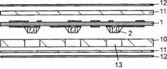
图4表示现有的无源部件内置式内插板的结构。在图4中,现有的无源部件内置式内插板由以下部分构成:在两面具有布线层8的两面布线基板1;安装在两面布线基板1的一面上的无源部件2;层压在两面布线基板1的安装有无源部件2的一面上的第二绝缘层3;层压在两面布线基板1的未安装无源部件2的另一面上的第一绝缘层4;层压在第二绝缘层3上的第二布线层6;层压在第一绝缘层4上的第一布线层5;以及电连接布线层8、第一布线层5和第二布线层6的通孔7,半导体元件9被安装在第二布线层6上。FIG. 4 shows the structure of a conventional passive component built-in interposer. In FIG. 4, the conventional passive component built-in interposer is composed of the following parts: a double-
但是,在现有的无源部件内置式内插板的结构中,无源部件2被配置在半导体元件9和基板内布线层之间,因此,用于连接半导体元件9和无源部件2的布线长度变长,例如,即使安装片状电容器(未图示)作为无源部件2,电源电压稳定化的效果也会变弱。而且,为了避免该问题,如图5所示,考虑使用两片两面布线基板1来缩短用于连接半导体元件9和无源部件2的布线长度,但是存在因使用两片高价的两面布线基板1从而造成成本变高的问题。而且,在使用两片两面布线基板1连接半导体元件9和无源部件2的结构中,需要预先定位布线了的图案之后形成通孔7,因此,增加了作业的工序数,在批量生产方面存在问题。However, in the structure of the conventional passive component built-in interposer, the
专利文献1:日本特开昭54-104564号公报Patent Document 1: Japanese Patent Application Laid-Open No. 54-104564
发明内容Contents of the invention
本发明是鉴于这样的问题而做出的,其以提供一种电气特性良好,且成本低、具有良好的批量生产性的无源部件内置式内插板为目的。The present invention has been made in view of such a problem, and an object of the present invention is to provide a passive component built-in interposer having good electrical characteristics, low cost, and good mass productivity.
本发明的无源部件内置式内插板的特征在于,其具备:树脂基板,其在两面具备布线层;一个以上的无源部件,其安装在位于树脂基板的一面上的布线层上;第一绝缘层,其层压在树脂基板的未安装无源部件的另一面上,并由织物和热固树脂构成,或由无纺布和热固树脂构成;第二绝缘层,其层压在树脂基板的安装有无源部件的上述一面上,并形成有比无源部件的外形尺寸大的空间,并由织物或无纺布和热固树脂构成;第一布线层,其形成在第一绝缘层的未与树脂基板接触的面上;第二布线层,其层压在第二绝缘层的未与树脂基板接触的面上;以及通孔,其电连接在树脂基板的两面上具备的布线层、第一布线层和第二布线层,第一布线层形成为能够安装半导体元件。The passive component built-in interposer of the present invention is characterized in that it includes: a resin substrate having wiring layers on both sides; one or more passive components mounted on the wiring layers on one side of the resin substrate; an insulating layer laminated on the other side of the resin substrate on which no passive components are mounted, and composed of fabric and thermosetting resin, or nonwoven fabric and thermosetting resin; a second insulating layer laminated on the On the above-mentioned side of the resin substrate on which the passive components are mounted, a space larger than the external dimensions of the passive components is formed, and is composed of fabric or non-woven fabric and thermosetting resin; the first wiring layer, which is formed on the first a surface of the insulating layer that is not in contact with the resin substrate; a second wiring layer laminated on the surface of the second insulating layer that is not in contact with the resin substrate; and via holes that are electrically connected to the A wiring layer, a first wiring layer, and a second wiring layer, the first wiring layer being formed to be capable of mounting a semiconductor element.
利用本发明,能够缩短用于电连接半导体元件和被内置的无源部件的布线长度,从而能够使电源电压稳定。因此,能够提供一种即使半导体元件的驱动频率变高,也可以使电路正常工作,且成本低、具有良好的批量生产性的无源部件内置式内插板。According to the present invention, it is possible to shorten the wiring length for electrically connecting the semiconductor element and the built-in passive components, thereby stabilizing the power supply voltage. Therefore, it is possible to provide a passive component built-in interposer that can operate normally even when the driving frequency of the semiconductor element is increased, is low in cost, and has good mass productivity.
附图说明Description of drawings
图1是本发明实施方式1及实施方式2中的无源部件内置式内插板的剖面图。FIG. 1 is a cross-sectional view of an interposer with built-in passive components in
图2A是本发明实施方式1中的无源部件内置式内插板的制造工序剖面图。2A is a cross-sectional view of the manufacturing process of the passive component built-in interposer in
图2B是本发明实施方式1中的无源部件内置式内插板的制造工序剖面2B is a sectional view of the manufacturing process of the passive component built-in interposer in
图2C是本发明实施方式1中的无源部件内置式内插板的制造工序剖面图。2C is a cross-sectional view of the manufacturing process of the passive component built-in interposer in
图2D是本发明实施方式1中的无源部件内置式内插板的制造工序剖面图。2D is a cross-sectional view of the manufacturing process of the passive component built-in interposer in
图2E是本发明实施方式1中的无源部件内置式内插板的制造工序剖面图。2E is a cross-sectional view of the manufacturing process of the passive component built-in interposer in
图2F是本发明实施方式1中的无源部件内置式内插板的制造工序剖面图。2F is a cross-sectional view of the manufacturing process of the passive component built-in interposer in
图3A是本发明实施方式2中的无源部件内置式内插板的制造工序剖面图。3A is a cross-sectional view showing a manufacturing process of an interposer with built-in passive components in
图3B是本发明实施方式2中的无源部件内置式内插板的制造工序剖面图。3B is a cross-sectional view of the manufacturing process of the passive component built-in interposer in
图3C是本发明实施方式2中的无源部件内置式内插板的制造工序剖面图。3C is a cross-sectional view of the manufacturing process of the passive component built-in interposer in
图3D是本发明实施方式2中的无源部件内置式内插板的制造工序剖面图。3D is a cross-sectional view of the manufacturing process of the passive component built-in interposer in
图3E是本发明实施方式2中的无源部件内置式内插板的制造工序剖面图。3E is a cross-sectional view of the manufacturing process of the passive component built-in interposer in
图3F是本发明实施方式2中的无源部件内置式内插板的制造工序剖面图。3F is a cross-sectional view of the manufacturing process of the passive component built-in interposer in
图4是现有的无源部件内置式内插板的剖面图。Fig. 4 is a sectional view of a conventional passive component built-in interposer.
图5是现有的无源部件内置式内插板的剖面图。Fig. 5 is a sectional view of a conventional passive component built-in interposer.
附图标记说明Explanation of reference signs
1 两面布线基板1 Double-sided wiring substrate
2 无源部件2 passive components
3 第二绝缘层3 second insulating layer
4 第一绝缘层4 The first insulating layer
5 第一布线层5 The first wiring layer
6 第二布线层6 Second wiring layer
7 通孔7 through holes
8 布线层8 wiring layers
9 半导体元件9 Semiconductor components
10、11 绝缘层10, 11 insulation layer
12 铜箔12 copper foil
13 开口部13 opening
14 贯通孔14 through hole
15 贯通孔内导通部15 Conducting part in the through hole
16 复合薄片16 composite sheets
具体实施方式Detailed ways
下面,使用附图详细说明本发明的实施方式。Hereinafter, embodiments of the present invention will be described in detail using the drawings.
(实施方式1)(Embodiment 1)
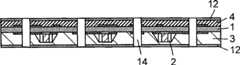
如图1所示,本发明实施方式1中的无源部件内置式内插板的特征在于,其具备:两面布线基板1,其在两面具备布线层8;无源部件2,其安装在位于该两面布线基板1的一面上的布线层8上;第一绝缘层4,其层压在两面布线基板1的未安装无源部件2的另一面上;第二绝缘层3,其层压在两面布线基板1的安装有无源部件2的上述一面上,并形成有比无源部件2的外形尺寸大的空间;第一布线层5,其层压在第一绝缘层4的未与两面布线基板1接触的面上;第二布线层6,其层压在第二绝缘层3的未与两面布线基板1接触的面上;以及通孔7,其用于电连接在两面布线基板1的两面上具备的布线层8与第一布线层及第二布线层5、6,第一布线层5形成为能够安装半导体元件9。As shown in FIG. 1 , the passive component built-in interposer in
这样,在设置在两面布线基板1的未安装无源部件2的上述另一面侧上的第一绝缘层4上,在未与两面布线基板1接触的面上设置第一布线层5,第一布线层5形成为能够安装半导体元件9,因此,即使是片状电容器或片状电阻等无源部件2的外形尺寸较大的情况,也能够缩短用于电连接无源部件2和半导体元件9的布线长度,从而可以减小电源布线中的电阻分量、线圈分量。因此,可以抑制用半导体元件9进行开关工作等电路工作时电压暂时下降的产生,从而可以使电源电压稳定。由此,在无源部件内置式内插板中,即使半导体元件9的驱动频率变高,也可以使电路正常工作。In this way, on the first insulating
两面布线基板1在基板的两面上具备布线层8,从而可安装片状电容器 或片状电阻等无源部件2。The double-
两面布线基板1及第一绝缘层4由织物或无纺布玻璃基材以及环氧树脂构成。并且,第二绝缘层3由环氧树脂和加入织物或无纺布玻璃基材的环氧树脂构成,并覆盖无源部件2。另外,作为热固树脂的环氧树脂可以是酚醛树脂(phenolic resin)。The double-
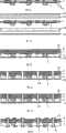
接着,使用图2A至图2F,说明无源部件内置式内插板的制造方法。Next, a method of manufacturing an interposer with built-in passive components will be described with reference to FIGS. 2A to 2F .
首先,如图2A所示,将无源部件2安装在两面具有布线层8的两面布线基板1的一面上。在采用使用引线键合(wire bonding)连接基板与LSI的树脂BGA基板(Ball Grid Array)的半导体封装结构中,内插板基板厚度通常规定在0.56mm±0.05mm。因此,作为为了遵循该厚度限制的条件,例如,使内置的片状电容器的厚度为0.22mm以下。First, as shown in FIG. 2A , a
具体地,作为安装在两面布线基板1的一面上的无源部件2,例如使用1005尺寸,0.15mmt的片状电容器。由此,对阻焊剂形成的限制减少,安装变得容易。另外,作为满足上述条件的电容器,也可使用0402尺寸的片状电容器。Specifically, as the
并且,对于两面布线基板1的布线层8与无源部件2的连接,一般使用焊锡,但也可使用导电性树脂粘合剂或熔点在接合后向高温侧变换的熔点可变焊锡膏。如果是后者的话,可避免焊锡流动等现象,因此,可无PSR地安装片状部件,即使进行制造后的回流焊,也可防止焊锡流动。由此,可安装受尺寸等限制的0402尺寸的无源部件2。Also, solder is generally used for connecting the
接着,如图2B所示,在两面布线基板1的安装有无源部件2的面上,按照无源部件2的配置层压具有开口部13的绝缘层10(未固化状态)、无开口部13的绝缘层11及铜箔12,同样地,在两面布线基板1的未安装无源部件2的面上,层压无开口部13的绝缘层11(未固化状态)和铜箔12。Next, as shown in FIG. 2B , on the surface of the double-
接着,以重叠的状态对该些两面布线基板1和绝缘层10、11和铜箔12进行加热同时加压。Next, these double-
首先,在环氧树脂软化的温度110℃下对未固化状态的具有开口部13的绝缘层10和无开口部13的绝缘层11加热同时加压约30分钟。First, uncured insulating
由此,具有开口部13的绝缘层10和无开口部13的绝缘层11的环氧树脂如图2C所示,熔化到开口部13内,由此覆盖无源部件2及无源部件2 下面的连接电极部分。Thus, the epoxy resin of the insulating
之后,如图2C所示,在加压状态下加热至200℃,使环氧树脂固化。由此,在两面布线基板1的安装有无源部件2的一面上形成第二绝缘层3,在两面布线基板1的未安装无源部件2的另一面上形成第一绝缘层4。Thereafter, as shown in FIG. 2C , the epoxy resin is cured by heating to 200° C. under pressure. Thus, the second insulating
接着,如图2D所示,在规定的位置上开设贯通孔14。之后,在该贯通孔14内,如图2E所示,设置通过镀敷形成的贯通孔内部导通部15,如图2F所示,图案化最外周部的铜箔。Next, as shown in FIG. 2D , through-
通过以上步骤,可以制成无源部件内置式内插板。Through the above steps, an interposer with built-in passive components can be manufactured.
根据这样的无源部件内置式内插板的结构,如图2D所示,在层压在最外周的布线层为铜箔12的状态下,加工贯通孔14时可以只以两面布线基板1的布线层8的图案形状为目标进行钻孔加工等,因此,具有容易对准位置,批量生产性良好的优点。According to the structure of such an interposer with built-in passive components, as shown in FIG. 2D , in the state where the wiring layer laminated on the outermost periphery is
并且,与使用两片高价的两面布线基板1的结构(图5)相比,使用一片两面布线基板1即可实现,因此可以降低成本。In addition, since it can be realized by using one double-
(实施方式2)(Embodiment 2)
如图1所示,本发明实施方式2中的无源部件内置式内插板具有与实施方式1中的无源部件内置式内插板一样的结构。即,其特征在于,其具备:两面布线基板1,其在两面上具备布线层8;无源部件2,其安装在位于该两面布线基板1的一面上的布线层8上;第一绝缘层4,其层压在两面布线基板1的未安装无源部件2的另一面上;第二绝缘层3,其层压在两面布线基板1的安装有无源部件2的上述一面上;第一布线层5,其层压在第一绝缘层4的未与两面布线基板1接触的面上;第二布线层6,其层压在第二绝缘层3的未与两面布线基板1接触的面上;以及通孔7,其电连接在两面布线基板1的两面上具备的布线层8与第一布线层及第二布线层5、6,第一布线层5形成为能够安装半导体元件9。As shown in FIG. 1 , the passive component built-in interposer in
两面布线基板1由玻璃基材和环氧树脂构成。并且,第一绝缘层4及第二绝缘层3由无机填料和环氧树脂构成。The double-
接着,使用图3A至图3F,说明本实施方式2中的无源部件内置式内插板的制造方法。Next, a method of manufacturing the passive component built-in interposer in
首先,如图3A所示,将无源部件2安装在两面具有布线层8的两面布线基板1的一面上。本实施方式中,也与实施方式1一样,作为安装的无 源部件使用1005尺寸、0.15mmt的片状电容器。First, as shown in FIG. 3A , a
对于此时的两面布线基板1的布线层8和无源部件2的连接,一般使用焊锡,但也可使用导电性树脂粘合剂或熔点在接合后向高温侧变换的熔点可变焊锡膏。例如,如果是后者的话,可避免焊锡流动等现象,因此,可无PSR地安装片状部件。由此,可容易地安装受尺寸限制的0402尺寸等的无源部件2。Solder is generally used to connect the
接着,如图3B所示,在安装有无源部件2的两面布线基板1的两面上,层压由无机填料和环氧树脂构成的复合薄片16和铜箔12。Next, as shown in FIG. 3B ,
接着,以重叠的状态加热同时加压这些两面布线基板1和复合薄片16以及铜箔12。Next, these double-
之后,如图3C所示,在加压状态下加热至200℃,使环氧树脂固化。由此,在两面布线基板1的安装有无源部件2的一面上形成第二绝缘层3,在两面布线基板1的未安装无源部件2的另一面上形成第一绝缘层4。Thereafter, as shown in FIG. 3C , the epoxy resin is cured by heating to 200° C. under pressure. Thus, the second insulating
接着,如图3D所示,在规定的位置上开设贯通孔14。之后,在该贯通孔14内,如图3E所示,设置通过镀敷形成的贯通孔内部导通部15,如图3F所示,图案化对最外周部的铜箔。Next, as shown in FIG. 3D , through-
通过以上步骤,可制成无源部件内置式内插板。该实施方式2中,除了具有实施方式1的效果,不需要预先在绝缘层上设置空间,因此,消除了种类对应性和绝缘层的对准位置的不良。由此,在无源部件内置式内插板的制造中,可实现批量生产性的提高。Through the above steps, an interposer with built-in passive components can be manufactured. In
另外,在实施方式1及实施方式2中,如图1所示,作为半导体元件9的安装方法,以引线键合法作为一个例子进行了说明,但是作为其它安装方法,也可使用倒装芯片安装。In addition, in
工业利用可能性Possibility of industrial use
如上所述,根据本发明,其成本低,具有良好的批量生产性,因此,容易实用化,可用作能够应对半导体元件的驱动频率的高频化的无源部件内置式内插板等。As described above, according to the present invention, it is low in cost and has good mass productivity, so it is easy to put into practical use, and can be used as a passive component built-in interposer and the like that can cope with the high frequency driving frequency of semiconductor elements.
Claims (6)
Translated fromChineseApplications Claiming Priority (3)
| Application Number | Priority Date | Filing Date | Title |
|---|---|---|---|
| JP323388/2006 | 2006-11-30 | ||
| JP2006323388 | 2006-11-30 | ||
| PCT/JP2007/072830WO2008066028A1 (en) | 2006-11-30 | 2007-11-27 | Interposer with built-in passive part |
Publications (2)
| Publication Number | Publication Date |
|---|---|
| CN101361182A CN101361182A (en) | 2009-02-04 |
| CN101361182Btrue CN101361182B (en) | 2011-09-14 |
Family
ID=39467815
Family Applications (1)
| Application Number | Title | Priority Date | Filing Date |
|---|---|---|---|
| CN2007800017000AExpired - Fee RelatedCN101361182B (en) | 2006-11-30 | 2007-11-27 | Interposer with built-in passive part |
Country Status (5)
| Country | Link |
|---|---|
| US (1) | US7968800B2 (en) |
| EP (1) | EP1950806A1 (en) |
| JP (1) | JP5093104B2 (en) |
| CN (1) | CN101361182B (en) |
| WO (1) | WO2008066028A1 (en) |
Families Citing this family (7)
| Publication number | Priority date | Publication date | Assignee | Title |
|---|---|---|---|---|
| US8072770B2 (en)* | 2008-10-14 | 2011-12-06 | Texas Instruments Incorporated | Semiconductor package with a mold material encapsulating a chip and a portion of a lead frame |
| KR101163222B1 (en)* | 2010-09-13 | 2012-07-06 | 에스케이하이닉스 주식회사 | Semiconductor package and method for manufacturing the same |
| KR101477392B1 (en)* | 2013-05-21 | 2014-12-29 | 삼성전기주식회사 | Electric component module |
| US9117807B2 (en)* | 2013-07-26 | 2015-08-25 | Infineon Technologies Ag | Integrated passives package, semiconductor module and method of manufacturing |
| CN103956326B (en)* | 2014-04-29 | 2017-01-11 | 华进半导体封装先导技术研发中心有限公司 | Manufacturing method for integrated passive interposer and corresponding integrated passive interposer |
| US10361149B2 (en)* | 2016-08-10 | 2019-07-23 | Qualcomm Incorporated | Land grid array (LGA) packaging of passive-on-glass (POG) structure |
| DE102017211513A1 (en) | 2017-07-06 | 2019-01-10 | Robert Bosch Gmbh | Electronic module and combination of an electronic module with a hydraulic plate |
Citations (1)
| Publication number | Priority date | Publication date | Assignee | Title |
|---|---|---|---|---|
| CN1722935A (en)* | 2004-07-14 | 2006-01-18 | 三星电机株式会社 | Method of fabricating PCB including embedded passive chip |
Family Cites Families (20)
| Publication number | Priority date | Publication date | Assignee | Title |
|---|---|---|---|---|
| JPS54104564A (en) | 1978-02-03 | 1979-08-16 | Shin Kobe Electric Machinery | Method of producing printed circuit board having electronic component elements on internal layer |
| US5530288A (en)* | 1994-10-12 | 1996-06-25 | International Business Machines Corporation | Passive interposer including at least one passive electronic component |
| US6274937B1 (en)* | 1999-02-01 | 2001-08-14 | Micron Technology, Inc. | Silicon multi-chip module packaging with integrated passive components and method of making |
| US6362525B1 (en)* | 1999-11-09 | 2002-03-26 | Cypress Semiconductor Corp. | Circuit structure including a passive element formed within a grid array substrate and method for making the same |
| US6407929B1 (en)* | 2000-06-29 | 2002-06-18 | Intel Corporation | Electronic package having embedded capacitors and method of fabrication therefor |
| US6346743B1 (en)* | 2000-06-30 | 2002-02-12 | Intel Corp. | Embedded capacitor assembly in a package |
| US6970362B1 (en)* | 2000-07-31 | 2005-11-29 | Intel Corporation | Electronic assemblies and systems comprising interposer with embedded capacitors |
| US6775150B1 (en)* | 2000-08-30 | 2004-08-10 | Intel Corporation | Electronic assembly comprising ceramic/organic hybrid substrate with embedded capacitors and methods of manufacture |
| JP2002319760A (en)* | 2001-04-20 | 2002-10-31 | Ngk Spark Plug Co Ltd | Method for manufacturing wiring board |
| US6933597B1 (en)* | 2002-07-09 | 2005-08-23 | National Semiconductor Corporation | Spacer with passive components for use in multi-chip modules |
| JP2004079701A (en)* | 2002-08-14 | 2004-03-11 | Sony Corp | Semiconductor device and its manufacturing method |
| JP2004343021A (en)* | 2003-03-17 | 2004-12-02 | Matsushita Electric Ind Co Ltd | Method and apparatus for manufacturing component built-in module |
| US7233061B1 (en)* | 2003-10-31 | 2007-06-19 | Xilinx, Inc | Interposer for impedance matching |
| US6875921B1 (en)* | 2003-10-31 | 2005-04-05 | Xilinx, Inc. | Capacitive interposer |
| EP1699277A4 (en)* | 2003-12-26 | 2007-08-15 | Murata Manufacturing Co | Ceramic multilayer substrate |
| US7446389B2 (en)* | 2004-06-17 | 2008-11-04 | Apple Inc. | Semiconductor die package with internal bypass capacitors |
| JP4865197B2 (en)* | 2004-06-30 | 2012-02-01 | ルネサスエレクトロニクス株式会社 | Semiconductor device and manufacturing method thereof |
| SG119230A1 (en)* | 2004-07-29 | 2006-02-28 | Micron Technology Inc | Interposer including at least one passive element at least partially defined by a recess formed therein method of manufacture system including same and wafer-scale interposer |
| US7613007B2 (en)* | 2004-12-21 | 2009-11-03 | E. I. Du Pont De Nemours And Company | Power core devices |
| JP4736451B2 (en) | 2005-02-03 | 2011-07-27 | パナソニック株式会社 | MULTILAYER WIRING BOARD, MANUFACTURING METHOD THEREOF, AND SEMICONDUCTOR PACKAGE AND ELECTRONIC DEVICE USING MULTILAYER WIRING BOARD |
- 2007
- 2007-11-27WOPCT/JP2007/072830patent/WO2008066028A1/ennot_activeCeased
- 2007-11-27USUS12/089,124patent/US7968800B2/ennot_activeExpired - Fee Related
- 2007-11-27JPJP2008513041Apatent/JP5093104B2/ennot_activeExpired - Fee Related
- 2007-11-27CNCN2007800017000Apatent/CN101361182B/ennot_activeExpired - Fee Related
- 2007-11-27EPEP07832555Apatent/EP1950806A1/ennot_activeWithdrawn
Patent Citations (1)
| Publication number | Priority date | Publication date | Assignee | Title |
|---|---|---|---|---|
| CN1722935A (en)* | 2004-07-14 | 2006-01-18 | 三星电机株式会社 | Method of fabricating PCB including embedded passive chip |
Non-Patent Citations (2)
| Title |
|---|
| JP特开2002-319760A 2002.10.31* |
| JP特开2006-216755A 2006.08.17* |
Also Published As
| Publication number | Publication date |
|---|---|
| EP1950806A1 (en) | 2008-07-30 |
| CN101361182A (en) | 2009-02-04 |
| WO2008066028A1 (en) | 2008-06-05 |
| JP5093104B2 (en) | 2012-12-05 |
| JPWO2008066028A1 (en) | 2010-04-22 |
| US7968800B2 (en) | 2011-06-28 |
| US20100155119A1 (en) | 2010-06-24 |
Similar Documents
| Publication | Publication Date | Title |
|---|---|---|
| CN101361182B (en) | Interposer with built-in passive part | |
| KR101496920B1 (en) | Semiconductor device | |
| JP2008226945A (en) | Semiconductor device and manufacturing method thereof | |
| CN104756615B (en) | Printed circuit board | |
| CN101853826A (en) | Connection parts and printed circuit board units | |
| US7820916B2 (en) | Composite ceramic substrate | |
| CN101502189B (en) | 3d electronic circuit device | |
| JP2009289802A (en) | Module having electronic part built-in and production method thereof | |
| WO2005071744A1 (en) | Multilayer electronic part and structure for mounting multilayer electronic part | |
| JPWO2011030542A1 (en) | Electronic component module and manufacturing method thereof | |
| JP5462450B2 (en) | Component built-in printed wiring board and method for manufacturing component built-in printed wiring board | |
| KR101139084B1 (en) | Multilayer printed circuit board and method of making same | |
| JP2005302854A (en) | Component built-in double-sided board, component built-in double-sided wiring board, and manufacturing method thereof | |
| JP5397012B2 (en) | Component built-in wiring board, method of manufacturing component built-in wiring board | |
| KR101167453B1 (en) | A printed circuit board comprising embeded electronic component within and a method for manufacturing | |
| KR101483874B1 (en) | Printed Circuit Board | |
| JP2008135483A (en) | Substrate incorporating electronic component and its manufacturing method | |
| JP5369875B2 (en) | Component built-in wiring board, method of manufacturing component built-in wiring board | |
| JP5221682B2 (en) | Printed circuit board and manufacturing method thereof | |
| KR100966341B1 (en) | Printed circuit board and manufacturing method thereof | |
| JP4814129B2 (en) | Wiring board with built-in components, Wiring board built-in components | |
| KR20150059086A (en) | Chip Embedded Board And Method Of Manufacturing The Same | |
| JP5601413B2 (en) | Component built-in wiring board, method of manufacturing component built-in wiring board | |
| KR20110131047A (en) | Embedded Printed Circuit Board Manufacturing Method and Embedded Printed Circuit Board Manufacturing Structure | |
| KR20140020015A (en) | Mounting structure of electronic component and mounting method thereof |
Legal Events
| Date | Code | Title | Description |
|---|---|---|---|
| C06 | Publication | ||
| PB01 | Publication | ||
| C10 | Entry into substantive examination | ||
| SE01 | Entry into force of request for substantive examination | ||
| C14 | Grant of patent or utility model | ||
| GR01 | Patent grant | ||
| CF01 | Termination of patent right due to non-payment of annual fee | ||
| CF01 | Termination of patent right due to non-payment of annual fee | Granted publication date:20110914 Termination date:20201127 |