CN101359605A - Method for Covalent Bonding at Room Temperature - Google Patents
Method for Covalent Bonding at Room TemperatureDownload PDFInfo
- Publication number
- CN101359605A CN101359605ACNA2008101340522ACN200810134052ACN101359605ACN 101359605 ACN101359605 ACN 101359605ACN A2008101340522 ACNA2008101340522 ACN A2008101340522ACN 200810134052 ACN200810134052 ACN 200810134052ACN 101359605 ACN101359605 ACN 101359605A
- Authority
- CN
- China
- Prior art keywords
- bonding
- layer
- oxide
- room temperature
- wafer
- Prior art date
- Legal status (The legal status is an assumption and is not a legal conclusion. Google has not performed a legal analysis and makes no representation as to the accuracy of the status listed.)
- Granted
Links
- 238000000034methodMethods0.000titleclaimsabstractdescription94
- 229910052731fluorineInorganic materials0.000claimsabstractdescription28
- 239000011737fluorineSubstances0.000claimsabstractdescription28
- YCKRFDGAMUMZLT-UHFFFAOYSA-NFluorine atomChemical compound[F]YCKRFDGAMUMZLT-UHFFFAOYSA-N0.000claimsabstractdescription27
- 230000008569processEffects0.000claimsdescription42
- 230000008021depositionEffects0.000claimsdescription15
- 238000010438heat treatmentMethods0.000claimsdescription6
- 239000007943implantSubstances0.000claimsdescription2
- 239000011248coating agentSubstances0.000claims13
- 238000000576coating methodMethods0.000claims13
- 239000010410layerSubstances0.000abstractdescription106
- VHUUQVKOLVNVRT-UHFFFAOYSA-NAmmonium hydroxideChemical compound[NH4+].[OH-]VHUUQVKOLVNVRT-UHFFFAOYSA-N0.000abstractdescription17
- 239000012790adhesive layerSubstances0.000abstractdescription17
- 235000011114ammonium hydroxideNutrition0.000abstractdescription17
- 230000015572biosynthetic processEffects0.000abstractdescription7
- 238000002513implantationMethods0.000abstractdescription4
- 235000012431wafersNutrition0.000description81
- 239000000758substrateSubstances0.000description44
- VYPSYNLAJGMNEJ-UHFFFAOYSA-NSilicium dioxideChemical compoundO=[Si]=OVYPSYNLAJGMNEJ-UHFFFAOYSA-N0.000description43
- 239000000463materialSubstances0.000description29
- XUIMIQQOPSSXEZ-UHFFFAOYSA-NSiliconChemical compound[Si]XUIMIQQOPSSXEZ-UHFFFAOYSA-N0.000description23
- 239000010703siliconSubstances0.000description23
- 229910052710siliconInorganic materials0.000description23
- XLYOFNOQVPJJNP-UHFFFAOYSA-NwaterChemical compoundOXLYOFNOQVPJJNP-UHFFFAOYSA-N0.000description21
- 238000000151depositionMethods0.000description17
- 229910001868waterInorganic materials0.000description17
- 239000000377silicon dioxideSubstances0.000description16
- 238000006243chemical reactionMethods0.000description15
- 229910020177SiOFInorganic materials0.000description13
- 238000009792diffusion processMethods0.000description13
- 238000000623plasma-assisted chemical vapour depositionMethods0.000description13
- 239000000243solutionSubstances0.000description13
- 241000894007speciesSpecies0.000description12
- 239000000126substanceSubstances0.000description12
- 229910052739hydrogenInorganic materials0.000description11
- 239000002184metalSubstances0.000description11
- 229910052751metalInorganic materials0.000description11
- 235000012239silicon dioxideNutrition0.000description11
- 239000006227byproductSubstances0.000description10
- 239000007789gasSubstances0.000description10
- 239000001257hydrogenSubstances0.000description10
- 229910052814silicon oxideInorganic materials0.000description10
- 230000003746surface roughnessEffects0.000description10
- UFHFLCQGNIYNRP-UHFFFAOYSA-NHydrogenChemical compound[H][H]UFHFLCQGNIYNRP-UHFFFAOYSA-N0.000description9
- 229910008051Si-OHInorganic materials0.000description9
- 229910006358Si—OHInorganic materials0.000description9
- 238000011282treatmentMethods0.000description9
- 238000007598dipping methodMethods0.000description8
- 238000003860storageMethods0.000description8
- 238000005470impregnationMethods0.000description7
- 239000004065semiconductorSubstances0.000description7
- 238000004544sputter depositionMethods0.000description7
- 239000000853adhesiveSubstances0.000description6
- 230000001070adhesive effectEffects0.000description6
- QVGXLLKOCUKJST-UHFFFAOYSA-Natomic oxygenChemical compound[O]QVGXLLKOCUKJST-UHFFFAOYSA-N0.000description6
- 238000004140cleaningMethods0.000description6
- 238000005516engineering processMethods0.000description6
- 239000001301oxygenSubstances0.000description6
- 229910052760oxygenInorganic materials0.000description6
- 238000001020plasma etchingMethods0.000description6
- 238000009832plasma treatmentMethods0.000description6
- 238000001004secondary ion mass spectrometryMethods0.000description6
- 229910008284Si—FInorganic materials0.000description5
- 238000000137annealingMethods0.000description5
- 239000003989dielectric materialSubstances0.000description5
- 238000005530etchingMethods0.000description5
- 230000010354integrationEffects0.000description5
- 238000005259measurementMethods0.000description5
- 238000012986modificationMethods0.000description5
- 230000004048modificationEffects0.000description5
- 238000005498polishingMethods0.000description5
- 239000002344surface layerSubstances0.000description5
- QGZKDVFQNNGYKY-UHFFFAOYSA-NAmmoniaChemical compoundNQGZKDVFQNNGYKY-UHFFFAOYSA-N0.000description4
- IJGRMHOSHXDMSA-UHFFFAOYSA-NAtomic nitrogenChemical compoundN#NIJGRMHOSHXDMSA-UHFFFAOYSA-N0.000description4
- 229910002808Si–O–SiInorganic materials0.000description4
- 230000008901benefitEffects0.000description4
- 230000000694effectsEffects0.000description4
- 238000007654immersionMethods0.000description4
- 238000004519manufacturing processMethods0.000description4
- 238000004806packaging method and processMethods0.000description4
- 102100021765E3 ubiquitin-protein ligase RNF139Human genes0.000description3
- 101001106970Homo sapiens E3 ubiquitin-protein ligase RNF139Proteins0.000description3
- 238000001994activationMethods0.000description3
- 238000013459approachMethods0.000description3
- 238000010586diagramMethods0.000description3
- 238000009616inductively coupled plasmaMethods0.000description3
- 238000006116polymerization reactionMethods0.000description3
- 238000012545processingMethods0.000description3
- QGZKDVFQNNGYKY-UHFFFAOYSA-OAmmoniumChemical compound[NH4+]QGZKDVFQNNGYKY-UHFFFAOYSA-O0.000description2
- XKRFYHLGVUSROY-UHFFFAOYSA-NArgonChemical compound[Ar]XKRFYHLGVUSROY-UHFFFAOYSA-N0.000description2
- 229910007991Si-NInorganic materials0.000description2
- 229910006294Si—NInorganic materials0.000description2
- 238000010521absorption reactionMethods0.000description2
- 238000004026adhesive bondingMethods0.000description2
- 238000004630atomic force microscopyMethods0.000description2
- 238000005229chemical vapour depositionMethods0.000description2
- 229910052681coesiteInorganic materials0.000description2
- 238000005336crackingMethods0.000description2
- 229910052906cristobaliteInorganic materials0.000description2
- 238000013461designMethods0.000description2
- 238000001035dryingMethods0.000description2
- 238000003682fluorination reactionMethods0.000description2
- 125000001153fluoro groupChemical groupF*0.000description2
- 238000009499grossingMethods0.000description2
- 125000002887hydroxy groupChemical group[H]O*0.000description2
- 239000012535impuritySubstances0.000description2
- 150000002500ionsChemical class0.000description2
- 239000007788liquidSubstances0.000description2
- 239000000203mixtureSubstances0.000description2
- 229910052757nitrogenInorganic materials0.000description2
- 229920002120photoresistant polymerPolymers0.000description2
- 239000011148porous materialSubstances0.000description2
- 239000002243precursorSubstances0.000description2
- 230000002441reversible effectEffects0.000description2
- 125000006850spacer groupChemical group0.000description2
- 229910052682stishoviteInorganic materials0.000description2
- 230000008646thermal stressEffects0.000description2
- 229910052905tridymiteInorganic materials0.000description2
- 238000007740vapor depositionMethods0.000description2
- NLXLAEXVIDQMFP-UHFFFAOYSA-NAmmonium chlorideSubstances[NH4+].[Cl-]NLXLAEXVIDQMFP-UHFFFAOYSA-N0.000description1
- 229910018557Si OInorganic materials0.000description1
- 229910052581Si3N4Inorganic materials0.000description1
- 229910004298SiO 2Inorganic materials0.000description1
- VYOZKLLJJHRFNA-UHFFFAOYSA-N[F].NChemical compound[F].NVYOZKLLJJHRFNA-UHFFFAOYSA-N0.000description1
- 230000004913activationEffects0.000description1
- 229910021529ammoniaInorganic materials0.000description1
- 239000000908ammonium hydroxideSubstances0.000description1
- 229910021417amorphous siliconInorganic materials0.000description1
- 239000007864aqueous solutionSubstances0.000description1
- 229910052786argonInorganic materials0.000description1
- 125000004429atomChemical group0.000description1
- 238000000071blow mouldingMethods0.000description1
- 238000010504bond cleavage reactionMethods0.000description1
- 239000013590bulk materialSubstances0.000description1
- 238000003486chemical etchingMethods0.000description1
- 230000002301combined effectEffects0.000description1
- 238000011109contaminationMethods0.000description1
- 238000000354decomposition reactionMethods0.000description1
- 230000007547defectEffects0.000description1
- 239000008367deionised waterSubstances0.000description1
- 229910021641deionized waterInorganic materials0.000description1
- 230000000994depressogenic effectEffects0.000description1
- 230000001627detrimental effectEffects0.000description1
- 238000010494dissociation reactionMethods0.000description1
- 230000005593dissociationsEffects0.000description1
- 238000001312dry etchingMethods0.000description1
- 230000008030eliminationEffects0.000description1
- 238000003379elimination reactionMethods0.000description1
- 238000005538encapsulationMethods0.000description1
- 238000004299exfoliationMethods0.000description1
- -1fluorine ionsChemical class0.000description1
- 239000011521glassSubstances0.000description1
- 238000000227grindingMethods0.000description1
- 230000036571hydrationEffects0.000description1
- 238000006703hydration reactionMethods0.000description1
- 230000005660hydrophilic surfaceEffects0.000description1
- 238000010348incorporationMethods0.000description1
- 238000003780insertionMethods0.000description1
- 230000037431insertionEffects0.000description1
- 239000012212insulatorSubstances0.000description1
- 239000012528membraneSubstances0.000description1
- 238000001465metallisationMethods0.000description1
- 150000002739metalsChemical class0.000description1
- 229910000069nitrogen hydrideInorganic materials0.000description1
- 238000010943off-gassingMethods0.000description1
- 230000005693optoelectronicsEffects0.000description1
- 230000003647oxidationEffects0.000description1
- 238000007254oxidation reactionMethods0.000description1
- 229920000642polymerPolymers0.000description1
- 238000002360preparation methodMethods0.000description1
- 230000001681protective effectEffects0.000description1
- 230000007017scissionEffects0.000description1
- 238000000926separation methodMethods0.000description1
- LIVNPJMFVYWSIS-UHFFFAOYSA-Nsilicon monoxideInorganic materials[Si-]#[O+]LIVNPJMFVYWSIS-UHFFFAOYSA-N0.000description1
- HQVNEWCFYHHQES-UHFFFAOYSA-Nsilicon nitrideChemical compoundN12[Si]34N5[Si]62N3[Si]51N64HQVNEWCFYHHQES-UHFFFAOYSA-N0.000description1
- 239000002210silicon-based materialSubstances0.000description1
- 239000002356single layerSubstances0.000description1
- 238000004528spin coatingMethods0.000description1
- 230000002269spontaneous effectEffects0.000description1
- 230000035882stressEffects0.000description1
- 238000006557surface reactionMethods0.000description1
- 238000004381surface treatmentMethods0.000description1
- TXEYQDLBPFQVAA-UHFFFAOYSA-NtetrafluoromethaneChemical compoundFC(F)(F)FTXEYQDLBPFQVAA-UHFFFAOYSA-N0.000description1
- 238000012876topographyMethods0.000description1
- 238000012546transferMethods0.000description1
- 238000009966trimmingMethods0.000description1
- 238000009834vaporizationMethods0.000description1
- 230000008016vaporizationEffects0.000description1
Images


Classifications
- B—PERFORMING OPERATIONS; TRANSPORTING
- B32—LAYERED PRODUCTS
- B32B—LAYERED PRODUCTS, i.e. PRODUCTS BUILT-UP OF STRATA OF FLAT OR NON-FLAT, e.g. CELLULAR OR HONEYCOMB, FORM
- B32B7/00—Layered products characterised by the relation between layers; Layered products characterised by the relative orientation of features between layers, or by the relative values of a measurable parameter between layers, i.e. products comprising layers having different physical, chemical or physicochemical properties; Layered products characterised by the interconnection of layers
- B32B7/04—Interconnection of layers
- H—ELECTRICITY
- H10—SEMICONDUCTOR DEVICES; ELECTRIC SOLID-STATE DEVICES NOT OTHERWISE PROVIDED FOR
- H10D—INORGANIC ELECTRIC SEMICONDUCTOR DEVICES
- H10D62/00—Semiconductor bodies, or regions thereof, of devices having potential barriers
- B—PERFORMING OPERATIONS; TRANSPORTING
- B81—MICROSTRUCTURAL TECHNOLOGY
- B81C—PROCESSES OR APPARATUS SPECIALLY ADAPTED FOR THE MANUFACTURE OR TREATMENT OF MICROSTRUCTURAL DEVICES OR SYSTEMS
- B81C1/00—Manufacture or treatment of devices or systems in or on a substrate
- B81C1/00349—Creating layers of material on a substrate
- B81C1/00357—Creating layers of material on a substrate involving bonding one or several substrates on a non-temporary support, e.g. another substrate
- H—ELECTRICITY
- H01—ELECTRIC ELEMENTS
- H01L—SEMICONDUCTOR DEVICES NOT COVERED BY CLASS H10
- H01L21/00—Processes or apparatus adapted for the manufacture or treatment of semiconductor or solid state devices or of parts thereof
- H01L21/02—Manufacture or treatment of semiconductor devices or of parts thereof
- H01L21/04—Manufacture or treatment of semiconductor devices or of parts thereof the devices having potential barriers, e.g. a PN junction, depletion layer or carrier concentration layer
- H01L21/18—Manufacture or treatment of semiconductor devices or of parts thereof the devices having potential barriers, e.g. a PN junction, depletion layer or carrier concentration layer the devices having semiconductor bodies comprising elements of Group IV of the Periodic Table or AIIIBV compounds with or without impurities, e.g. doping materials
- H01L21/30—Treatment of semiconductor bodies using processes or apparatus not provided for in groups H01L21/20 - H01L21/26
- H01L21/31—Treatment of semiconductor bodies using processes or apparatus not provided for in groups H01L21/20 - H01L21/26 to form insulating layers thereon, e.g. for masking or by using photolithographic techniques; After treatment of these layers; Selection of materials for these layers
- H01L21/3105—After-treatment
- H—ELECTRICITY
- H01—ELECTRIC ELEMENTS
- H01L—SEMICONDUCTOR DEVICES NOT COVERED BY CLASS H10
- H01L21/00—Processes or apparatus adapted for the manufacture or treatment of semiconductor or solid state devices or of parts thereof
- H01L21/70—Manufacture or treatment of devices consisting of a plurality of solid state components formed in or on a common substrate or of parts thereof; Manufacture of integrated circuit devices or of parts thereof
- H01L21/71—Manufacture of specific parts of devices defined in group H01L21/70
- H01L21/76—Making of isolation regions between components
- H01L21/762—Dielectric regions, e.g. EPIC dielectric isolation, LOCOS; Trench refilling techniques, SOI technology, use of channel stoppers
- H01L21/7624—Dielectric regions, e.g. EPIC dielectric isolation, LOCOS; Trench refilling techniques, SOI technology, use of channel stoppers using semiconductor on insulator [SOI] technology
- H01L21/76251—Dielectric regions, e.g. EPIC dielectric isolation, LOCOS; Trench refilling techniques, SOI technology, use of channel stoppers using semiconductor on insulator [SOI] technology using bonding techniques
- H—ELECTRICITY
- H01—ELECTRIC ELEMENTS
- H01L—SEMICONDUCTOR DEVICES NOT COVERED BY CLASS H10
- H01L24/00—Arrangements for connecting or disconnecting semiconductor or solid-state bodies; Methods or apparatus related thereto
- H01L24/01—Means for bonding being attached to, or being formed on, the surface to be connected, e.g. chip-to-package, die-attach, "first-level" interconnects; Manufacturing methods related thereto
- H01L24/26—Layer connectors, e.g. plate connectors, solder or adhesive layers; Manufacturing methods related thereto
- H01L24/28—Structure, shape, material or disposition of the layer connectors prior to the connecting process
- H01L24/29—Structure, shape, material or disposition of the layer connectors prior to the connecting process of an individual layer connector
- H—ELECTRICITY
- H01—ELECTRIC ELEMENTS
- H01L—SEMICONDUCTOR DEVICES NOT COVERED BY CLASS H10
- H01L24/00—Arrangements for connecting or disconnecting semiconductor or solid-state bodies; Methods or apparatus related thereto
- H01L24/80—Methods for connecting semiconductor or other solid state bodies using means for bonding being attached to, or being formed on, the surface to be connected
- H01L24/81—Methods for connecting semiconductor or other solid state bodies using means for bonding being attached to, or being formed on, the surface to be connected using a bump connector
- H—ELECTRICITY
- H01—ELECTRIC ELEMENTS
- H01L—SEMICONDUCTOR DEVICES NOT COVERED BY CLASS H10
- H01L24/00—Arrangements for connecting or disconnecting semiconductor or solid-state bodies; Methods or apparatus related thereto
- H01L24/80—Methods for connecting semiconductor or other solid state bodies using means for bonding being attached to, or being formed on, the surface to be connected
- H01L24/83—Methods for connecting semiconductor or other solid state bodies using means for bonding being attached to, or being formed on, the surface to be connected using a layer connector
- H—ELECTRICITY
- H01—ELECTRIC ELEMENTS
- H01L—SEMICONDUCTOR DEVICES NOT COVERED BY CLASS H10
- H01L24/00—Arrangements for connecting or disconnecting semiconductor or solid-state bodies; Methods or apparatus related thereto
- H01L24/91—Methods for connecting semiconductor or solid state bodies including different methods provided for in two or more of groups H01L24/80 - H01L24/90
- H01L24/92—Specific sequence of method steps
- H—ELECTRICITY
- H10—SEMICONDUCTOR DEVICES; ELECTRIC SOLID-STATE DEVICES NOT OTHERWISE PROVIDED FOR
- H10D—INORGANIC ELECTRIC SEMICONDUCTOR DEVICES
- H10D48/00—Individual devices not covered by groups H10D1/00 - H10D44/00
- H10D48/30—Devices controlled by electric currents or voltages
- H10D48/32—Devices controlled by only the electric current supplied, or only the electric potential applied, to an electrode which does not carry the current to be rectified, amplified or switched
- H10D48/34—Bipolar devices
- B—PERFORMING OPERATIONS; TRANSPORTING
- B32—LAYERED PRODUCTS
- B32B—LAYERED PRODUCTS, i.e. PRODUCTS BUILT-UP OF STRATA OF FLAT OR NON-FLAT, e.g. CELLULAR OR HONEYCOMB, FORM
- B32B2250/00—Layers arrangement
- B32B2250/04—4 layers
- B—PERFORMING OPERATIONS; TRANSPORTING
- B81—MICROSTRUCTURAL TECHNOLOGY
- B81C—PROCESSES OR APPARATUS SPECIALLY ADAPTED FOR THE MANUFACTURE OR TREATMENT OF MICROSTRUCTURAL DEVICES OR SYSTEMS
- B81C2201/00—Manufacture or treatment of microstructural devices or systems
- B81C2201/01—Manufacture or treatment of microstructural devices or systems in or on a substrate
- B81C2201/0174—Manufacture or treatment of microstructural devices or systems in or on a substrate for making multi-layered devices, film deposition or growing
- B81C2201/019—Bonding or gluing multiple substrate layers
- B—PERFORMING OPERATIONS; TRANSPORTING
- B81—MICROSTRUCTURAL TECHNOLOGY
- B81C—PROCESSES OR APPARATUS SPECIALLY ADAPTED FOR THE MANUFACTURE OR TREATMENT OF MICROSTRUCTURAL DEVICES OR SYSTEMS
- B81C2203/00—Forming microstructural systems
- B81C2203/01—Packaging MEMS
- B81C2203/0118—Bonding a wafer on the substrate, i.e. where the cap consists of another wafer
- B—PERFORMING OPERATIONS; TRANSPORTING
- B81—MICROSTRUCTURAL TECHNOLOGY
- B81C—PROCESSES OR APPARATUS SPECIALLY ADAPTED FOR THE MANUFACTURE OR TREATMENT OF MICROSTRUCTURAL DEVICES OR SYSTEMS
- B81C2203/00—Forming microstructural systems
- B81C2203/01—Packaging MEMS
- B81C2203/0172—Seals
- B81C2203/019—Seals characterised by the material or arrangement of seals between parts
- H—ELECTRICITY
- H01—ELECTRIC ELEMENTS
- H01L—SEMICONDUCTOR DEVICES NOT COVERED BY CLASS H10
- H01L2224/00—Indexing scheme for arrangements for connecting or disconnecting semiconductor or solid-state bodies and methods related thereto as covered by H01L24/00
- H01L2224/01—Means for bonding being attached to, or being formed on, the surface to be connected, e.g. chip-to-package, die-attach, "first-level" interconnects; Manufacturing methods related thereto
- H01L2224/02—Bonding areas; Manufacturing methods related thereto
- H01L2224/04—Structure, shape, material or disposition of the bonding areas prior to the connecting process
- H01L2224/0401—Bonding areas specifically adapted for bump connectors, e.g. under bump metallisation [UBM]
- H—ELECTRICITY
- H01—ELECTRIC ELEMENTS
- H01L—SEMICONDUCTOR DEVICES NOT COVERED BY CLASS H10
- H01L2224/00—Indexing scheme for arrangements for connecting or disconnecting semiconductor or solid-state bodies and methods related thereto as covered by H01L24/00
- H01L2224/01—Means for bonding being attached to, or being formed on, the surface to be connected, e.g. chip-to-package, die-attach, "first-level" interconnects; Manufacturing methods related thereto
- H01L2224/02—Bonding areas; Manufacturing methods related thereto
- H01L2224/07—Structure, shape, material or disposition of the bonding areas after the connecting process
- H01L2224/08—Structure, shape, material or disposition of the bonding areas after the connecting process of an individual bonding area
- H01L2224/0805—Shape
- H01L2224/08057—Shape in side view
- H01L2224/08059—Shape in side view comprising protrusions or indentations
- H—ELECTRICITY
- H01—ELECTRIC ELEMENTS
- H01L—SEMICONDUCTOR DEVICES NOT COVERED BY CLASS H10
- H01L2224/00—Indexing scheme for arrangements for connecting or disconnecting semiconductor or solid-state bodies and methods related thereto as covered by H01L24/00
- H01L2224/01—Means for bonding being attached to, or being formed on, the surface to be connected, e.g. chip-to-package, die-attach, "first-level" interconnects; Manufacturing methods related thereto
- H01L2224/26—Layer connectors, e.g. plate connectors, solder or adhesive layers; Manufacturing methods related thereto
- H01L2224/28—Structure, shape, material or disposition of the layer connectors prior to the connecting process
- H01L2224/29—Structure, shape, material or disposition of the layer connectors prior to the connecting process of an individual layer connector
- H01L2224/29001—Core members of the layer connector
- H01L2224/29099—Material
- H01L2224/29186—Material with a principal constituent of the material being a non metallic, non metalloid inorganic material
- H—ELECTRICITY
- H01—ELECTRIC ELEMENTS
- H01L—SEMICONDUCTOR DEVICES NOT COVERED BY CLASS H10
- H01L2224/00—Indexing scheme for arrangements for connecting or disconnecting semiconductor or solid-state bodies and methods related thereto as covered by H01L24/00
- H01L2224/80—Methods for connecting semiconductor or other solid state bodies using means for bonding being attached to, or being formed on, the surface to be connected
- H01L2224/80001—Methods for connecting semiconductor or other solid state bodies using means for bonding being attached to, or being formed on, the surface to be connected by connecting a bonding area directly to another bonding area, i.e. connectorless bonding, e.g. bumpless bonding
- H01L2224/808—Bonding techniques
- H01L2224/80894—Direct bonding, i.e. joining surfaces by means of intermolecular attracting interactions at their interfaces, e.g. covalent bonds, van der Waals forces
- H01L2224/80896—Direct bonding, i.e. joining surfaces by means of intermolecular attracting interactions at their interfaces, e.g. covalent bonds, van der Waals forces between electrically insulating surfaces, e.g. oxide or nitride layers
- H—ELECTRICITY
- H01—ELECTRIC ELEMENTS
- H01L—SEMICONDUCTOR DEVICES NOT COVERED BY CLASS H10
- H01L2224/00—Indexing scheme for arrangements for connecting or disconnecting semiconductor or solid-state bodies and methods related thereto as covered by H01L24/00
- H01L2224/80—Methods for connecting semiconductor or other solid state bodies using means for bonding being attached to, or being formed on, the surface to be connected
- H01L2224/80001—Methods for connecting semiconductor or other solid state bodies using means for bonding being attached to, or being formed on, the surface to be connected by connecting a bonding area directly to another bonding area, i.e. connectorless bonding, e.g. bumpless bonding
- H01L2224/80986—Specific sequence of steps, e.g. repetition of manufacturing steps, time sequence
- H—ELECTRICITY
- H01—ELECTRIC ELEMENTS
- H01L—SEMICONDUCTOR DEVICES NOT COVERED BY CLASS H10
- H01L2224/00—Indexing scheme for arrangements for connecting or disconnecting semiconductor or solid-state bodies and methods related thereto as covered by H01L24/00
- H01L2224/80—Methods for connecting semiconductor or other solid state bodies using means for bonding being attached to, or being formed on, the surface to be connected
- H01L2224/81—Methods for connecting semiconductor or other solid state bodies using means for bonding being attached to, or being formed on, the surface to be connected using a bump connector
- H01L2224/818—Bonding techniques
- H01L2224/81894—Direct bonding, i.e. joining surfaces by means of intermolecular attracting interactions at their interfaces, e.g. covalent bonds, van der Waals forces
- H01L2224/81895—Direct bonding, i.e. joining surfaces by means of intermolecular attracting interactions at their interfaces, e.g. covalent bonds, van der Waals forces between electrically conductive surfaces, e.g. copper-copper direct bonding, surface activated bonding
- H—ELECTRICITY
- H01—ELECTRIC ELEMENTS
- H01L—SEMICONDUCTOR DEVICES NOT COVERED BY CLASS H10
- H01L2224/00—Indexing scheme for arrangements for connecting or disconnecting semiconductor or solid-state bodies and methods related thereto as covered by H01L24/00
- H01L2224/80—Methods for connecting semiconductor or other solid state bodies using means for bonding being attached to, or being formed on, the surface to be connected
- H01L2224/83—Methods for connecting semiconductor or other solid state bodies using means for bonding being attached to, or being formed on, the surface to be connected using a layer connector
- H01L2224/8319—Arrangement of the layer connectors prior to mounting
- H—ELECTRICITY
- H01—ELECTRIC ELEMENTS
- H01L—SEMICONDUCTOR DEVICES NOT COVERED BY CLASS H10
- H01L2224/00—Indexing scheme for arrangements for connecting or disconnecting semiconductor or solid-state bodies and methods related thereto as covered by H01L24/00
- H01L2224/80—Methods for connecting semiconductor or other solid state bodies using means for bonding being attached to, or being formed on, the surface to be connected
- H01L2224/83—Methods for connecting semiconductor or other solid state bodies using means for bonding being attached to, or being formed on, the surface to be connected using a layer connector
- H01L2224/838—Bonding techniques
- H01L2224/8385—Bonding techniques using a polymer adhesive, e.g. an adhesive based on silicone, epoxy, polyimide, polyester
- H—ELECTRICITY
- H01—ELECTRIC ELEMENTS
- H01L—SEMICONDUCTOR DEVICES NOT COVERED BY CLASS H10
- H01L2224/00—Indexing scheme for arrangements for connecting or disconnecting semiconductor or solid-state bodies and methods related thereto as covered by H01L24/00
- H01L2224/80—Methods for connecting semiconductor or other solid state bodies using means for bonding being attached to, or being formed on, the surface to be connected
- H01L2224/83—Methods for connecting semiconductor or other solid state bodies using means for bonding being attached to, or being formed on, the surface to be connected using a layer connector
- H01L2224/838—Bonding techniques
- H01L2224/83894—Direct bonding, i.e. joining surfaces by means of intermolecular attracting interactions at their interfaces, e.g. covalent bonds, van der Waals forces
- H01L2224/83896—Direct bonding, i.e. joining surfaces by means of intermolecular attracting interactions at their interfaces, e.g. covalent bonds, van der Waals forces between electrically insulating surfaces, e.g. oxide or nitride layers
- H—ELECTRICITY
- H01—ELECTRIC ELEMENTS
- H01L—SEMICONDUCTOR DEVICES NOT COVERED BY CLASS H10
- H01L2224/00—Indexing scheme for arrangements for connecting or disconnecting semiconductor or solid-state bodies and methods related thereto as covered by H01L24/00
- H01L2224/91—Methods for connecting semiconductor or solid state bodies including different methods provided for in two or more of groups H01L2224/80 - H01L2224/90
- H01L2224/92—Specific sequence of method steps
- H01L2224/9202—Forming additional connectors after the connecting process
- H—ELECTRICITY
- H01—ELECTRIC ELEMENTS
- H01L—SEMICONDUCTOR DEVICES NOT COVERED BY CLASS H10
- H01L2224/00—Indexing scheme for arrangements for connecting or disconnecting semiconductor or solid-state bodies and methods related thereto as covered by H01L24/00
- H01L2224/91—Methods for connecting semiconductor or solid state bodies including different methods provided for in two or more of groups H01L2224/80 - H01L2224/90
- H01L2224/92—Specific sequence of method steps
- H01L2224/921—Connecting a surface with connectors of different types
- H01L2224/9212—Sequential connecting processes
- H01L2224/92122—Sequential connecting processes the first connecting process involving a bump connector
- H01L2224/92125—Sequential connecting processes the first connecting process involving a bump connector the second connecting process involving a layer connector
- H—ELECTRICITY
- H01—ELECTRIC ELEMENTS
- H01L—SEMICONDUCTOR DEVICES NOT COVERED BY CLASS H10
- H01L2924/00—Indexing scheme for arrangements or methods for connecting or disconnecting semiconductor or solid-state bodies as covered by H01L24/00
- H01L2924/01—Chemical elements
- H01L2924/01004—Beryllium [Be]
- H—ELECTRICITY
- H01—ELECTRIC ELEMENTS
- H01L—SEMICONDUCTOR DEVICES NOT COVERED BY CLASS H10
- H01L2924/00—Indexing scheme for arrangements or methods for connecting or disconnecting semiconductor or solid-state bodies as covered by H01L24/00
- H01L2924/01—Chemical elements
- H01L2924/01005—Boron [B]
- H—ELECTRICITY
- H01—ELECTRIC ELEMENTS
- H01L—SEMICONDUCTOR DEVICES NOT COVERED BY CLASS H10
- H01L2924/00—Indexing scheme for arrangements or methods for connecting or disconnecting semiconductor or solid-state bodies as covered by H01L24/00
- H01L2924/01—Chemical elements
- H01L2924/01006—Carbon [C]
- H—ELECTRICITY
- H01—ELECTRIC ELEMENTS
- H01L—SEMICONDUCTOR DEVICES NOT COVERED BY CLASS H10
- H01L2924/00—Indexing scheme for arrangements or methods for connecting or disconnecting semiconductor or solid-state bodies as covered by H01L24/00
- H01L2924/01—Chemical elements
- H01L2924/01013—Aluminum [Al]
- H—ELECTRICITY
- H01—ELECTRIC ELEMENTS
- H01L—SEMICONDUCTOR DEVICES NOT COVERED BY CLASS H10
- H01L2924/00—Indexing scheme for arrangements or methods for connecting or disconnecting semiconductor or solid-state bodies as covered by H01L24/00
- H01L2924/01—Chemical elements
- H01L2924/01015—Phosphorus [P]
- H—ELECTRICITY
- H01—ELECTRIC ELEMENTS
- H01L—SEMICONDUCTOR DEVICES NOT COVERED BY CLASS H10
- H01L2924/00—Indexing scheme for arrangements or methods for connecting or disconnecting semiconductor or solid-state bodies as covered by H01L24/00
- H01L2924/01—Chemical elements
- H01L2924/01016—Sulfur [S]
- H—ELECTRICITY
- H01—ELECTRIC ELEMENTS
- H01L—SEMICONDUCTOR DEVICES NOT COVERED BY CLASS H10
- H01L2924/00—Indexing scheme for arrangements or methods for connecting or disconnecting semiconductor or solid-state bodies as covered by H01L24/00
- H01L2924/01—Chemical elements
- H01L2924/01018—Argon [Ar]
- H—ELECTRICITY
- H01—ELECTRIC ELEMENTS
- H01L—SEMICONDUCTOR DEVICES NOT COVERED BY CLASS H10
- H01L2924/00—Indexing scheme for arrangements or methods for connecting or disconnecting semiconductor or solid-state bodies as covered by H01L24/00
- H01L2924/01—Chemical elements
- H01L2924/01019—Potassium [K]
- H—ELECTRICITY
- H01—ELECTRIC ELEMENTS
- H01L—SEMICONDUCTOR DEVICES NOT COVERED BY CLASS H10
- H01L2924/00—Indexing scheme for arrangements or methods for connecting or disconnecting semiconductor or solid-state bodies as covered by H01L24/00
- H01L2924/01—Chemical elements
- H01L2924/01023—Vanadium [V]
- H—ELECTRICITY
- H01—ELECTRIC ELEMENTS
- H01L—SEMICONDUCTOR DEVICES NOT COVERED BY CLASS H10
- H01L2924/00—Indexing scheme for arrangements or methods for connecting or disconnecting semiconductor or solid-state bodies as covered by H01L24/00
- H01L2924/01—Chemical elements
- H01L2924/01033—Arsenic [As]
- H—ELECTRICITY
- H01—ELECTRIC ELEMENTS
- H01L—SEMICONDUCTOR DEVICES NOT COVERED BY CLASS H10
- H01L2924/00—Indexing scheme for arrangements or methods for connecting or disconnecting semiconductor or solid-state bodies as covered by H01L24/00
- H01L2924/01—Chemical elements
- H01L2924/01039—Yttrium [Y]
- H—ELECTRICITY
- H01—ELECTRIC ELEMENTS
- H01L—SEMICONDUCTOR DEVICES NOT COVERED BY CLASS H10
- H01L2924/00—Indexing scheme for arrangements or methods for connecting or disconnecting semiconductor or solid-state bodies as covered by H01L24/00
- H01L2924/01—Chemical elements
- H01L2924/01058—Cerium [Ce]
- H—ELECTRICITY
- H01—ELECTRIC ELEMENTS
- H01L—SEMICONDUCTOR DEVICES NOT COVERED BY CLASS H10
- H01L2924/00—Indexing scheme for arrangements or methods for connecting or disconnecting semiconductor or solid-state bodies as covered by H01L24/00
- H01L2924/01—Chemical elements
- H01L2924/01067—Holmium [Ho]
- H—ELECTRICITY
- H01—ELECTRIC ELEMENTS
- H01L—SEMICONDUCTOR DEVICES NOT COVERED BY CLASS H10
- H01L2924/00—Indexing scheme for arrangements or methods for connecting or disconnecting semiconductor or solid-state bodies as covered by H01L24/00
- H01L2924/01—Chemical elements
- H01L2924/01072—Hafnium [Hf]
- H—ELECTRICITY
- H01—ELECTRIC ELEMENTS
- H01L—SEMICONDUCTOR DEVICES NOT COVERED BY CLASS H10
- H01L2924/00—Indexing scheme for arrangements or methods for connecting or disconnecting semiconductor or solid-state bodies as covered by H01L24/00
- H01L2924/01—Chemical elements
- H01L2924/01074—Tungsten [W]
- H—ELECTRICITY
- H01—ELECTRIC ELEMENTS
- H01L—SEMICONDUCTOR DEVICES NOT COVERED BY CLASS H10
- H01L2924/00—Indexing scheme for arrangements or methods for connecting or disconnecting semiconductor or solid-state bodies as covered by H01L24/00
- H01L2924/01—Chemical elements
- H01L2924/01075—Rhenium [Re]
- H—ELECTRICITY
- H01—ELECTRIC ELEMENTS
- H01L—SEMICONDUCTOR DEVICES NOT COVERED BY CLASS H10
- H01L2924/00—Indexing scheme for arrangements or methods for connecting or disconnecting semiconductor or solid-state bodies as covered by H01L24/00
- H01L2924/01—Chemical elements
- H01L2924/01082—Lead [Pb]
- H—ELECTRICITY
- H01—ELECTRIC ELEMENTS
- H01L—SEMICONDUCTOR DEVICES NOT COVERED BY CLASS H10
- H01L2924/00—Indexing scheme for arrangements or methods for connecting or disconnecting semiconductor or solid-state bodies as covered by H01L24/00
- H01L2924/06—Polymers
- H01L2924/078—Adhesive characteristics other than chemical
- H01L2924/07802—Adhesive characteristics other than chemical not being an ohmic electrical conductor
- H—ELECTRICITY
- H01—ELECTRIC ELEMENTS
- H01L—SEMICONDUCTOR DEVICES NOT COVERED BY CLASS H10
- H01L2924/00—Indexing scheme for arrangements or methods for connecting or disconnecting semiconductor or solid-state bodies as covered by H01L24/00
- H01L2924/10—Details of semiconductor or other solid state devices to be connected
- H01L2924/102—Material of the semiconductor or solid state bodies
- H01L2924/1025—Semiconducting materials
- H01L2924/10251—Elemental semiconductors, i.e. Group IV
- H01L2924/10253—Silicon [Si]
- H—ELECTRICITY
- H01—ELECTRIC ELEMENTS
- H01L—SEMICONDUCTOR DEVICES NOT COVERED BY CLASS H10
- H01L2924/00—Indexing scheme for arrangements or methods for connecting or disconnecting semiconductor or solid-state bodies as covered by H01L24/00
- H01L2924/10—Details of semiconductor or other solid state devices to be connected
- H01L2924/11—Device type
- H01L2924/13—Discrete devices, e.g. 3 terminal devices
- H01L2924/1304—Transistor
- H01L2924/1305—Bipolar Junction Transistor [BJT]
- H—ELECTRICITY
- H01—ELECTRIC ELEMENTS
- H01L—SEMICONDUCTOR DEVICES NOT COVERED BY CLASS H10
- H01L2924/00—Indexing scheme for arrangements or methods for connecting or disconnecting semiconductor or solid-state bodies as covered by H01L24/00
- H01L2924/10—Details of semiconductor or other solid state devices to be connected
- H01L2924/11—Device type
- H01L2924/14—Integrated circuits
- H—ELECTRICITY
- H01—ELECTRIC ELEMENTS
- H01L—SEMICONDUCTOR DEVICES NOT COVERED BY CLASS H10
- H01L2924/00—Indexing scheme for arrangements or methods for connecting or disconnecting semiconductor or solid-state bodies as covered by H01L24/00
- H01L2924/10—Details of semiconductor or other solid state devices to be connected
- H01L2924/146—Mixed devices
- H01L2924/1461—MEMS
- H—ELECTRICITY
- H01—ELECTRIC ELEMENTS
- H01L—SEMICONDUCTOR DEVICES NOT COVERED BY CLASS H10
- H01L2924/00—Indexing scheme for arrangements or methods for connecting or disconnecting semiconductor or solid-state bodies as covered by H01L24/00
- H01L2924/30—Technical effects
- H01L2924/35—Mechanical effects
- H01L2924/351—Thermal stress
- Y—GENERAL TAGGING OF NEW TECHNOLOGICAL DEVELOPMENTS; GENERAL TAGGING OF CROSS-SECTIONAL TECHNOLOGIES SPANNING OVER SEVERAL SECTIONS OF THE IPC; TECHNICAL SUBJECTS COVERED BY FORMER USPC CROSS-REFERENCE ART COLLECTIONS [XRACs] AND DIGESTS
- Y10—TECHNICAL SUBJECTS COVERED BY FORMER USPC
- Y10T—TECHNICAL SUBJECTS COVERED BY FORMER US CLASSIFICATION
- Y10T156/00—Adhesive bonding and miscellaneous chemical manufacture
- Y10T156/10—Methods of surface bonding and/or assembly therefor
- Y—GENERAL TAGGING OF NEW TECHNOLOGICAL DEVELOPMENTS; GENERAL TAGGING OF CROSS-SECTIONAL TECHNOLOGIES SPANNING OVER SEVERAL SECTIONS OF THE IPC; TECHNICAL SUBJECTS COVERED BY FORMER USPC CROSS-REFERENCE ART COLLECTIONS [XRACs] AND DIGESTS
- Y10—TECHNICAL SUBJECTS COVERED BY FORMER USPC
- Y10T—TECHNICAL SUBJECTS COVERED BY FORMER US CLASSIFICATION
- Y10T428/00—Stock material or miscellaneous articles
- Y10T428/24—Structurally defined web or sheet [e.g., overall dimension, etc.]
- Y10T428/24355—Continuous and nonuniform or irregular surface on layer or component [e.g., roofing, etc.]
- Y—GENERAL TAGGING OF NEW TECHNOLOGICAL DEVELOPMENTS; GENERAL TAGGING OF CROSS-SECTIONAL TECHNOLOGIES SPANNING OVER SEVERAL SECTIONS OF THE IPC; TECHNICAL SUBJECTS COVERED BY FORMER USPC CROSS-REFERENCE ART COLLECTIONS [XRACs] AND DIGESTS
- Y10—TECHNICAL SUBJECTS COVERED BY FORMER USPC
- Y10T—TECHNICAL SUBJECTS COVERED BY FORMER US CLASSIFICATION
- Y10T428/00—Stock material or miscellaneous articles
- Y10T428/24—Structurally defined web or sheet [e.g., overall dimension, etc.]
- Y10T428/24942—Structurally defined web or sheet [e.g., overall dimension, etc.] including components having same physical characteristic in differing degree
- Y—GENERAL TAGGING OF NEW TECHNOLOGICAL DEVELOPMENTS; GENERAL TAGGING OF CROSS-SECTIONAL TECHNOLOGIES SPANNING OVER SEVERAL SECTIONS OF THE IPC; TECHNICAL SUBJECTS COVERED BY FORMER USPC CROSS-REFERENCE ART COLLECTIONS [XRACs] AND DIGESTS
- Y10—TECHNICAL SUBJECTS COVERED BY FORMER USPC
- Y10T—TECHNICAL SUBJECTS COVERED BY FORMER US CLASSIFICATION
- Y10T428/00—Stock material or miscellaneous articles
- Y10T428/31504—Composite [nonstructural laminate]
- Y10T428/31678—Of metal
Landscapes
- Engineering & Computer Science (AREA)
- Microelectronics & Electronic Packaging (AREA)
- Computer Hardware Design (AREA)
- Power Engineering (AREA)
- Manufacturing & Machinery (AREA)
- Physics & Mathematics (AREA)
- Condensed Matter Physics & Semiconductors (AREA)
- General Physics & Mathematics (AREA)
- Pressure Welding/Diffusion-Bonding (AREA)
- Formation Of Insulating Films (AREA)
Abstract
Translated fromChineseDescription
Translated fromChinese本申请是申请号为200480018125.1、申请日为2004年5月19日、发明标题为“室温共价粘结的方法”的分案申请。This application is a divisional application with the application number 200480018125.1, the filing date is May 19, 2004, and the title of the invention is "method for covalent bonding at room temperature".
发明背景Background of the invention
发明领域field of invention
本发明涉及室温下晶片的直接粘结领域,和更特别地,涉及利用氟和铵的效果和组合效果制造工程基底用基底的粘结,包封,和在电介质中,特别是在氧化硅层中三维器件整合。This invention relates to the field of direct bonding of wafers at room temperature, and more particularly, to the bonding of substrates for the manufacture of engineered substrates utilizing the effects and combined effects of fluorine and ammonium, encapsulation, and in dielectrics, especially silicon oxide layers Integration of 3D devices.
相关领域的说明Description of related fields
由于逼近常规CMOS器件的物理极限,和对高性能电子系统需求急切,因此,芯片上系统(system-on-a chip)(SOC)成为半导体工业的自然解决方法。对于芯片上系统的制备来说,要求在芯片上的各种功能。尽管硅技术是加工大量器件的主要支持技术,但现在可由除了硅以外的材料制造的单独的器件和/或电路最佳地获得许多所需的电路和光电功能。因此,将非硅基器件与硅基器件整合的杂化系统具有提供独特的SOC功能的潜力,这种独特的功能不可能获自于单独的纯硅或者纯的非硅器件。Due to the approaching physical limits of conventional CMOS devices and the urgent need for high-performance electronic systems, system-on-a-chip (SOC) has become a natural solution for the semiconductor industry. For the fabrication of a system on a chip, various functions on the chip are required. Although silicon technology is the primary enabling technology for processing a large number of devices, many desired circuit and optoelectronic functions are now optimally obtained from individual devices and/or circuits fabricated from materials other than silicon. Therefore, hybrid systems that integrate non-silicon-based devices with silicon-based devices have the potential to provide unique SOC functionality that cannot be obtained from pure silicon or pure non-silicon devices alone.
混杂器件整合的一种方法是在硅上不相类似的材料的异质外延生长(hetero-epitaxial)。迄今为止,认识到这种异质外延生长在异质外延生长的膜内的高密度缺陷,这主要是由于在非硅膜和基底之间晶格常数的错配所致。One approach to hybrid device integration is the hetero-epitaxial growth of dissimilar materials on silicon. To date, such heteroepitaxially grown high density defects in heteroepitaxially grown films have been recognized, mainly due to a lattice constant mismatch between the non-silicon film and the substrate.
混杂器件整合的另一方法是晶片粘结技术。然而,在升高的温度下热膨胀系数不同的不相类似的材料的晶片粘结引入热应力,所述热应力可导致错位生成、解粘结或龟裂。因此,希望低温粘结。对于粘结不相类似的材料来说,若不相类似的材料包括具有低分解温度的材料或者温敏器件,例如InP异质结双极晶体管或具有超浅源极和漏极曲线(profile)的加工过的Si器件,低温粘结也是所需的。Another approach to hybrid device integration is die-bonding technology. However, wafer bonding of dissimilar materials with different coefficients of thermal expansion at elevated temperatures introduces thermal stresses that can lead to dislocation generation, debonding, or cracking. Therefore, low temperature bonding is desired. For bonding dissimilar materials, if dissimilar materials include materials with low decomposition temperatures or temperature sensitive devices such as InP heterojunction bipolar transistors or with ultra-shallow source and drain profiles For processed Si devices, low temperature bonding is also required.
在含有不同材料的相同芯片上生产不同功能所需的工艺设计是困难的,且难以优化。确实,许多所得SOC芯片(特别是较大的整合尺寸的那些)显示出低的产率。一种方法是通过晶片粘合剂粘结和层的转移,互连充分加工的IC。参见,例如Y.Hayashi,S.Wada,K.Kajiyana,K.Oyama,R.Koh,S.Takahashi和T.Kunio,Symp.VLSI Tech.Dig.95(1990)和美国专利5563084,这两篇参考文献的全部内容在此通过参考引入。然而,晶片粘合剂粘结通常在升高的温度下操作,且缺点是,产生热应力、脱气、气泡形成和粘合剂的不稳定,从而导致在该工艺中降低的产率和随着时间流逝可靠度差。粘合剂也可与典型的半导体制造工艺不兼容。此外,粘合剂粘结通常不是气密的。The process design required to produce different functions on the same chip containing different materials is difficult and difficult to optimize. Indeed, many of the resulting SOC chips (especially those of larger integration size) show low yields. One approach is to interconnect fully processed ICs by wafer adhesive bonding and layer transfer. See, for example, Y.Hayashi, S.Wada, K.Kajiyana, K.Oyama, R.Koh, S.Takahashi and T.Kunio, Symp.VLSI Tech.Dig.95 (1990) and U.S. Patent 5,563,084, both The entire contents of the references are hereby incorporated by reference. However, wafer adhesive bonding typically operates at elevated temperatures, and has the disadvantages of thermal stress, outgassing, bubble formation, and instability of the adhesive, resulting in reduced yields and subsequent failures in the process. Poor reliability over time. Adhesives can also be incompatible with typical semiconductor manufacturing processes. Furthermore, adhesive bonds are generally not airtight.
室温晶片直接粘结是使得在没有使用任何粘合剂的情况下,可在室温下粘结晶片,从而导致气密粘结的技术。在这种粘合剂粘结内不容易引入应力和不均匀度。此外,若低温粘结的晶片对可耐受修磨(thinning)的话,则对于特定的材料组合来说,当粘结对(bonded pair)中的一块晶片被修磨到小于相应临界值的厚度时,避免了在该层内生成不匹配位错和在随后的热处理步骤期间粘结对的滑动或龟裂。参见,例如Q.-Y.Tong和U.
发明概述Summary of the invention
本发明涉及粘结方法,其中包括在相应的第一和第二元件上形成第一和第二粘结层,其中至少一层粘结层包括氟化氧化物层,使第一和第二粘结层在室温下在环境中接触,并在室温下,在所述第一和第二层之间形成粘结。The present invention relates to a method of bonding comprising forming first and second bonding layers on respective first and second components, wherein at least one bonding layer comprises a fluorinated oxide layer such that the first and second bonding The junction layers are in ambient contact at room temperature and form a bond between the first and second layers at room temperature.
形成所述至少一层含氟化氧化物层的粘结层可包括形成氧化物层并将该层暴露于含氟溶液、蒸汽或者气体下。Forming the tie layer of the at least one fluorinated oxide layer may include forming an oxide layer and exposing the layer to a fluorine-containing solution, vapor or gas.
形成本发明粘结结构的方法也可包括粘结第一和第二粘结层,并在第一和第二粘结层之间的界面附近处,形成具有第一峰值的氟浓度,和独立于第一峰值并且远离第一峰值处,在至少一层所述第一和第二层内形成第二峰值。粘结层之一可以是氧化物层,该方法进一步包括将氟引入到氧化物层内,并在引入步骤之后,在第一氧化物层上形成第二氧化物层。The method of forming the bonding structure of the present invention may also include bonding the first and second bonding layers, and forming a fluorine concentration having a first peak near the interface between the first and second bonding layers, and independently At and away from the first peak, a second peak is formed in at least one of said first and second layers. One of the bonding layers may be an oxide layer, and the method further includes introducing fluorine into the oxide layer, and after the introducing step, forming a second oxide layer on the first oxide layer.
本发明还涉及具有第一和第二元件的粘结结构体,其中分别在第一和第二元件上形成第一和第二粘结层,第一粘结层以非粘合剂的方式粘结到第二粘结层上,和第一粘结层包括氟化氧化物。在该结构体中,第一粘结层可包括在第二氧化物层上形成的第一氧化物层,其中在第一粘结层内的氟浓度具有位于第一和第二粘结层之间的界面附近的第一峰值,和第二峰值位于第一和第二氧化物层之间的界面处。The present invention also relates to a bonded structure having first and second elements, wherein first and second adhesive layers are respectively formed on the first and second elements, the first adhesive layer being adhered in a non-adhesive manner. bonded to the second adhesive layer, and the first adhesive layer includes a fluorinated oxide. In the structure, the first bonding layer may include a first oxide layer formed on the second oxide layer, wherein the concentration of fluorine in the first bonding layer has a concentration between the first and second bonding layers a first peak near the interface between the first and second oxide layers, and a second peak at the interface between the first and second oxide layers.
本发明的目的是在室温下,在空气中,在氧化硅覆盖的各种材料的晶片的表面上,实现非常高密度的共价粘结。The object of the present invention is to achieve very high density covalent bonding at room temperature in air on the surface of wafers of various materials covered with silicon oxide.
本发明进一步的目的是降低厚度为纳米到微米的表面氧化硅层的密度。A further object of the present invention is to reduce the density of the surface silicon oxide layer having a thickness of nanometers to micrometers.
本发明再一目的是提高杂质和/或吸收的湿气离开粘结界面的扩散速度。It is a further object of the present invention to increase the rate of diffusion of impurities and/or absorbed moisture away from the bonding interface.
本发明另一目的是获得在表面上氟浓度大于1×1017cm-3的粘结层(厚度为纳米到微米)。Another object of the present invention is to obtain a bonding layer (thickness ranging from nanometers to micrometers) with a fluorine concentration on the surface greater than 1×1017 cm−3 .
本发明额外的目的是使用标准半导体方法,在集成电路或器件图案的表面上改变共价粘结体的密度。An additional object of the present invention is to vary the density of covalent bonds on the surface of an integrated circuit or device pattern using standard semiconductor methods.
本发明另一目的是通过标准半导体方法,采用氟化处理,在氧化硅表面上局部或全部形成低-k电介质。Another object of the present invention is to partially or completely form a low-k dielectric on a silicon oxide surface by a fluorination process by standard semiconductor methods.
本发明再进一步的目的是生成其表面可用所需基团在原子水平上终止的材料,以便当两个这样的表面在室温下接触时形成共价粘结体。A still further object of the present invention is to generate materials whose surfaces can be terminated at the atomic level with desired groups so as to form a covalent bond when two such surfaces are brought into contact at room temperature.
附图简述Brief description of the drawings
可容易获得本发明的更全面理解和许多附带的优点,这是因为通过参考下述详细说明,当与附图结合考虑时,可更好地理解它们,其中:A fuller understanding of the present invention and its many attendant advantages may readily be obtained as they are better understood by reference to the following detailed description when considered in conjunction with the accompanying drawings, in which:
图1是根据本发明实施方案的流程图;Figure 1 is a flow chart according to an embodiment of the present invention;
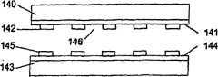
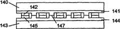
图2A是具有相应粘结层的一对解粘结基底的示意图;Figure 2A is a schematic illustration of a pair of debonded substrates with corresponding bonding layers;
图2B是一对彼此接触的解粘结基底的示意图;Figure 2B is a schematic illustration of a pair of debonded substrates in contact with each other;
图2C是在除去一部分基底之后,在图2B中的一对基底的示意图;Figure 2C is a schematic illustration of the pair of substrates in Figure 2B after removing a portion of the substrate;
图2D是在粘结第三基底之后,在图2C中的一对基底的示意图;Figure 2D is a schematic diagram of the pair of substrates in Figure 2C after bonding a third substrate;
图3是在粘结晶片对的气氛中,在有和无含氟与铵的粘结层的情况下,室温粘结能作为储存时间函数的图表;Figure 3 is a graph of room temperature bonding energy as a function of storage time with and without a fluorine- and ammonium-containing bonding layer in an atmosphere for bonding wafer pairs;
图4是对于有和无等离子处理处理情况下加工的粘结晶片来说,粘结能作为储存时间函数的图表;Figure 4 is a graph of bonding energy as a function of storage time for bonded wafers processed with and without plasma treatment;
图5是对于有和无铵情况下处理的晶片对来说,在室温下,粘结能作为储存时间函数的图表;Figure 5 is a graph of bonding energy as a function of storage time at room temperature for pairs of wafers treated with and without ammonium;
图6是室温粘结能作为后-HF处理烘烤温度函数的图表;Figure 6 is a graph of room temperature bonding energy as a function of post-HF treatment bake temperature;
图7是说明所测量的粘结能和储存时间的均方根之间线性关系的图表;Figure 7 is a graph illustrating the linear relationship between measured bonding energy and the root mean square of storage time;
图8A-8C说明了其中在粘结层内形成氟化层的本发明的实施方案;8A-8C illustrate an embodiment of the invention in which a fluorinated layer is formed within a tie layer;
图9A-9E图示了在粘结晶片对内局部充分地共价粘结的区域;9A-9E illustrate locally substantially covalently bonded regions within a bonded wafer pair;
图10是描述在本发明的粘结界面下方断裂的Si基底表面下的显微照片;Figure 10 is a photomicrograph depicting a subsurface Si substrate fractured below the bonding interface of the present invention;
图11是包埋的低-k氧化物结构体的示意图;Figure 11 is a schematic diagram of an embedded low-k oxide structure;
图12是SIMS(次级离子质谱)测量结果;Fig. 12 is SIMS (secondary ion mass spectrometry) measurement result;
图13说明了将多个器件粘结到较大的基底上;Figure 13 illustrates the bonding of multiple devices to a larger substrate;
图14A-14C图示了本发明粘结方法在金属对金属粘结上的应用;14A-14C illustrate the application of the bonding method of the present invention to metal-to-metal bonding;
图15说明了多个器件金属对金属地粘结到较大基底上;和Figure 15 illustrates the metal-to-metal bonding of multiple devices to a larger substrate; and
图16A-16E说明了本发明的气密封装应用。16A-16E illustrate the hermetic packaging application of the present invention.
优选实施方案的详细说明Detailed Description of the Preferred Embodiment
现参考附图,其中在数幅附图中,类似的参考标记表示类似或者相应的部分,和更特别地描述图1和图2A-2B,其说明了本发明粘结方法的第一个实施方案。图1用通用的术语说明了本发明的方法。在待粘结的元件,例如基底或者晶片上形成粘结层(步骤10)。通过例如将粘结层的表面暴露于氟或氟植入剂下,从而氟化至少一层粘结层(步骤11)。使各层直接接触,从而形成粘结界面(步骤12),并通过化学反应导致形成共价键(步骤13)。随着额外共价键形成和/或来自所述化学反应的副产物扩散离开所述粘结界面,粘结强度会增加。优选地,粘结工艺在室温下,例如在约20-25℃下进行。Referring now to the drawings, in which like reference numerals indicate like or corresponding parts throughout the several views, and more particularly to FIGS. 1 and 2A-2B, which illustrate a first implementation of the bonding method of the present invention plan. Figure 1 illustrates the method of the invention in general terms. An adhesive layer is formed on the components to be bonded, such as substrates or wafers (step 10). At least one tie layer is fluorinated (step 11 ), for example by exposing the surface of the tie layer to fluorine or a fluorine implant. The layers are brought into direct contact, forming a cohesive interface (step 12), and a chemical reaction leads to the formation of a covalent bond (step 13). Bond strength increases as additional covalent bonds are formed and/or by-products from the chemical reactions diffuse away from the bond interface. Preferably, the bonding process is performed at room temperature, eg at about 20-25°C.
图2A示出了具有相应粘结层201、204和相应的相对表面202、205的两块晶片200、203。粘结层201和204由通过许多技术,其中包括,但不限于溅射、等离子加强的气相沉积中的任何一种或其结合形成的氧化硅,或由热氧化物形成。材料201和204的表面可以相对粗糙(>20埃RMS)且要求在直接接触之前变光滑。该膜也可具有足够低的表面粗糙度,在没有变光滑的情况下粘结。可使用申请WO01/61734、WO01/26137和WO01/71797中所述的技术制备表面202和205,产生光滑、活化的表面。FIG. 2A shows two
层201和204可以是使用化学气相沉积(CVD)或者等离子加强的CVD(PECVD)、溅射或者通过气化形成的绝缘体,例如SiO2、氮化硅、无定形硅。也可使用其它材料,例如聚合物,半导体或者烧结材料。层201和204的厚度应当大于相应基底201和203的表面形貌。
使用例如化学-机械抛光,平面化层201和204的表面202和205并使之变光滑。优选抛光表面202和205到约不大于3nm的粗糙度,和优选不大于约0.1nm,且基本上是平坦的。表面粗糙度值典型地以均方根(RMS)值的形式给出。此外,表面粗糙度可以以平均值形式给出,它几乎与RMS值相同。在抛光之后,清洗表面202和205,并干燥,以便从抛光步骤中除去任何残渣。抛光的表面201和205优选然后用溶液漂洗。
在抛光粘结层的表面到(如上所述的)小的表面粗糙度之后,视需要,将粘结层暴露于氟化处理下,例如稀释的含水HF、CF4或SF6等离子处理、F+植入下,视需要,加热,以氟化所有或所需部分的粘结层。如下所述,活化该层,并用所需基团在表面上终止。活化和终止步骤可一起进行。可如此处理粘结表面中的仅仅一个或者两个。After polishing the surface of the bonding layer to a small surface roughness (as described above), the bonding layer is optionally exposed to a fluorinated treatment, such as diluted aqueous HF, CF4 or SF6 plasma treatment, F+ Under implantation, heat, if necessary, to fluorinate all or desired portions of the bonding layer. This layer is activated and terminated on the surface with the desired groups as described below. The activation and termination steps can be performed together. Only one or two of the bonding surfaces may be so treated.
表面201和205然后进行活化工艺。这一活化工艺是蚀刻工艺,且优选是非常轻微的蚀刻(VSE)工艺。术语VSE是指非常轻微蚀刻的表面的均方根微粗糙度(micro-roughness)(RMS)保持接近于未蚀刻的数值,典型地<0.5nm,和优选在0.1nm-3nm范围内。所除去的材料的最佳量取决于除去所使用的材料和方法。所除去的典型量从数埃变化到数纳米。还可除去更多的材料。VSE还包括使在处理表面上的粘结断裂,和可在没有大量除去材料的情况下发生。VSE不同于通过例如在表面上引入电荷或者破坏表面层的简单的表面改性。在本发明方法的第一个实施例中,VSE方法由在特定的功率电平下,经特定时间的气体或者混合气体(例如氧气、氩气、氮气、CF4、NH3)的等离子工艺组成。等离子工艺的功率和持续时间将随获得所需粘结能所使用的材料而变化。以下给出了实例,但一般来说,根据经验确定功率和持续时间。
可以按照不同模式进行等离子工艺。可使用反应性离子蚀刻(RIE)和等离子体模式这二者,以及电感耦合等离子体模式(ICP)。也可使用溅射。以下给出了RIE和等离子体模式中的数据和实例。The plasma process can be performed in different modes. Both reactive ion etching (RIE) and plasma modes can be used, as well as inductively coupled plasma mode (ICP). Sputtering can also be used. Data and examples in RIE and plasma modes are given below.
VSE工艺通过物理溅射和/或化学反应非常轻微地蚀刻表面,且优选控制VSE工艺,使粘结表面的表面粗糙度不劣化。取决于VSE和所蚀刻的材料,可甚至改进表面粗糙度。对于本发明的室温粘结方法来说,不过度蚀刻表面34的任何气体或者气体混合物可用于本发明的室温粘结方法。The VSE process etches the surface very slightly by physical sputtering and/or chemical reaction, and the VSE process is preferably controlled so that the surface roughness of the bonding surface is not degraded. Depending on the VSE and the material being etched, the surface roughness may even be improved. For the room temperature bonding method of the present invention, any gas or gas mixture that does not over etch surface 34 may be used in the room temperature bonding method of the present invention.
VSE起到清洗表面的作用并使晶片表面上的氧化物化学键断裂。CSE方法因此可显著提高表面活性。通过合适设计VSE,所需的粘结物种可用于在VSE过程中终止表面表面201和205。或者,可使用后VSE处理,其中在后VSE工艺过程中,用所需的终止物种活化并终止表面。The VSE acts to clean the surface and break the oxide chemical bonds on the wafer surface. The CSE method can thus significantly increase surface activity. By properly designing the VSE, the desired bonding species can be used to terminate
所需的物种进一步优选与表面原子层形成临时粘结,从而有效地终止原子层,直到随后这一表面可与通过相同或者另一粘结物种终止的表面结合在一起。在表面上的所需物种当它们足够接近时,进一步优选彼此反应,从而使得在低温或者室温下在表面201和205之间提供化学粘结,其中所述化学粘结通过已反应的所需物种扩散或者解离并扩散远离粘结界面来加强。The desired species further preferably forms a temporary bond with the atomic layer of the surface, effectively terminating the atomic layer until later this surface can be bonded together with a surface terminated by the same or another binding species. The desired species on the surfaces further preferably react with each other when they are in close enough proximity such that a chemical bond is provided between the
后VSE工艺优选包括在含选择化学品的溶液内浸渍,产生表面反应,所述表面反应导致用所需物种终止粘结表面34。浸渍优选就在VSE工艺之后进行。后VSE工艺可在与进行VSE工艺相同的装置内进行。如果VSE和后VSE工艺二者是或者干燥工艺,即等离子体、RIE、ICP、溅射等工艺,或者湿工艺,即,溶液浸渍的话,这可最容易进行。所需物种优选由一层单层或数层单层原子或分子组成。The post-VSE process preferably involves immersion in a solution containing the selected chemicals to create a surface reaction that results in termination of the bonding surface 34 with the desired species. Impregnation is preferably performed immediately after the VSE process. The post-VSE process can be performed in the same apparatus as the VSE process. This can be done most easily if both the VSE and post-VSE processes are either dry processes, ie plasma, RIE, ICP, sputtering, etc. processes, or wet processes, ie solution immersion. The desired species preferably consists of a monolayer or several monolayers of atoms or molecules.
后VSE工艺也可由等离子体、RIE或者其它干燥工艺组成,其中合适的气体化学品被引入,导致用所需物种终止该表面。后VSE工艺也可以是第二VSE工艺。终止工艺也可包括清洗工艺,其中在没有VSE的情况下除去表面污染物。在此情况下,类似于以上所述的后VSE工艺的后清洗工艺导致所需的表面终止。Post-VSE processes may also consist of plasma, RIE or other drying processes in which suitable gas chemicals are introduced resulting in termination of the surface with the desired species. The post-VSE process may also be a second VSE process. The termination process may also include a cleaning process in which surface contamination is removed without VSE. In this case, a post-cleaning process similar to the post-VSE process described above results in the desired surface termination.
若通过清洗或者VSE工艺活化的表面粘结随后足够弱地表面再构,且在粘结之前,可充分维持清洁,以便随后与类似表面的粘结可形成化学键的话,则后VSE或者后清洗工艺可以需要或者可以不需要用所需的物种终止表面。A post-VSE or post-cleaning process can be used if a surface activated by a cleaning or VSE process is subsequently resurfaced weakly enough and clean enough to be maintained prior to bonding so that subsequent bonding to a similar surface can form a chemical bond. It may or may not be necessary to terminate the surface with the desired species.
任选地漂洗晶片,然后干燥。(视需要)通过校准两块晶片,并使之结合在一起,形成粘结界面,从而粘结它们。The wafer is optionally rinsed and then dried. (Optional) Bond the two wafers by aligning them and bringing them together to form a bonding interface.
如图2B所示,表面202和205彼此直接接触,形成粘结的结构体。在室温下,在两个表面202和205之间的界面206上发生共价键合。然后典型地在粘结界面内的一些位置处发生自发粘结,并在晶片上生长。随着起始的化学键开始生长,当表面足够接近时,在终止表面202和205所使用的物种之间发生导致化学键的化学反应,例如聚合。粘结能定义为在通过插入楔子(wedge)部分解粘结的粘结界面处独立的表面之一的特定表面能。在所述粘结表面彼此接触之后,随着时间流逝,当共价键的数量增加和/或来自于所述终止表面结合在一起形成的反应副产物扩散离开所述粘结表面时,在所述粘结的结构体内的粘结强度增加。反应副产物扩散离开粘结界面到晶片边缘上或者被晶片吸收,典型地被周围材料内的晶片被吸收。该副产物也可转化成扩散离开晶片或者被晶片吸收的其它副产物。可通过除去转化的物种,来增加共价和/或离子键的数量,从而导致粘结强度的进一步增加。As shown in Figure 2B, surfaces 202 and 205 are in direct contact with each other, forming a bonded structure. At room temperature, covalent bonding occurs at the
实施例Example
在第一个实施方案的第一个实施例中,在200-250℃下,PECVD(等离子加强的化学清洗沉积)二氧化硅沉积在单侧抛光的硅片上。PECVD氧化物的厚度不是关键的,和任意地选择为~1.0微米。抛光用PECVD氧化物层覆盖的晶片,使表面变光滑。使用AFM(原子力显微术),测定表面微粗糙度的RMS(均方根)数值为1-3埃。通过改性的RCA1(H2O∶H2O2∶NH4OH=5∶1∶0.25)溶液清洗晶片并旋转干燥。In a first example of the first embodiment, PECVD (plasma enhanced chemical cleaning deposition) silicon dioxide was deposited on a single side polished silicon wafer at 200-250°C. The thickness of the PECVD oxide is not critical, and is arbitrarily chosen to be ~1.0 microns. Polish the wafer covered with the PECVD oxide layer to smooth the surface. Using AFM (Atomic Force Microscopy), the RMS (Root Mean Square) value of the surface microroughness is determined to be 1-3 Angstroms. The wafer was cleaned by a modified RCA1 (H2 O:H 2 O2 :NH4 OH=5:1:0.25) solution and spin-dried.
将晶片任意地分成数组,其中在粘结之前,在一组内的每一晶片对以特定方式处理。在第I组中,在100mTorr下,氧化物覆盖的晶片对在氧气等离子体内以反应性离子蚀刻模式(RIE)处理30秒。等离子处理的晶片浸渍在含有35%氨水的CMOS级的氢氧化铵水溶液(下文称为“NH4OH”)中,之后旋转干燥,并在室温下,在空气中粘结。在第II组中,氧化物覆盖的晶片浸渍在0.025%HF水溶液中30秒,并旋转干燥。可根据所使用的氧化硅的类型改变HF浓度,和可以是0.01%-0.5%。然后在空气中,在250℃下加热晶片2-10小时。再次在RCA1中清洗晶片,氧气等离子体处理,在NH4OH中浸渍,并旋转干燥,之后在室温下在空气中粘结。The wafers are arbitrarily divided into groups, where each wafer pair within a group is treated in a specific manner prior to bonding. In Group I, oxide-covered wafer pairs were treated in reactive ion etch mode (RIE) in an oxygen plasma at 100 mTorr for 30 seconds. The plasma-treated wafers were dipped in a CMOS-grade aqueous ammonium hydroxide solution (hereinafter "NH4OH ") containing 35% ammonia, then spin-dried, and bonded in air at room temperature. In group II, oxide-covered wafers were dipped in 0.025% aqueous HF for 30 seconds and spin-dried. The HF concentration can vary depending on the type of silicon oxide used, and can be 0.01%-0.5%. The wafer was then heated at 250°C for 2-10 hours in air. The wafers were again cleaned in RCA1, oxygen plasma treated, dipped inNH4OH , and spin dried before bonding in air at room temperature.
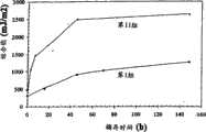
图3分别示出了在室温下,在空气中,第I组和第II组的粘结的晶片对的粘结能作为储存时间的函数。在第II组内的晶片对的粘结能在3小时内快速增加到1000mJ/m2,并在空气中,在室温下,~40小时储存之后,达到本体硅的断裂能(2500mJ/m2)且显著高于第I组晶片对。这通过图3上部的曲线示出。在室温粘结之前,HF浸渍和随后加热在第I组和第II组粘结晶片之间产生室温粘结能的巨大差别。Figure 3 shows the bonding energy as a function of storage time for the bonded wafer pairs of Group I and Group II, respectively, at room temperature in air. The bonding energy of wafer pairs within Group II rapidly increased to 1000 mJ/m2 within 3 hours and reached the fracture energy of bulk silicon (2500 mJ/m2 after ~40 hours storage in air at room temperature ) and significantly higher than that of group I wafer pair. This is shown by the upper curve in FIG. 3 . HF dipping followed by heating prior to room temperature bonding produced a large difference in room temperature bonding energy between Group I and Group II bonded wafers.
为了测定氧气等离子处理在提高室温粘结能方面的效果,制备另一组(第III组)晶片。在与第II组晶片对相同的工艺条件下处理,所不同的是省去氧气等离子处理步骤,之后在室温下粘结第III组内氧化物覆盖的晶片对。对于有和无等离子处理的晶片对来说,在室温下实现类似的粘结能,如图4所示。图4表明,若通过HF含水浸渍和烘烤,之后进行晶片粘结,则对于在室温下的充分化学键合来说,氧气等离子处理不是重要的。To determine the effect of oxygen plasma treatment in increasing room temperature bond energy, another set (Group III) of wafers was prepared. Treated under the same process conditions as Group II wafer pairs, except that the oxygen plasma treatment step was omitted, the oxide-covered wafer pairs in Group III were subsequently bonded at room temperature. Similar bonding energies were achieved at room temperature for wafer pairs with and without plasma treatment, as shown in FIG. 4 . Figure 4 shows that oxygen plasma treatment is not critical for adequate chemical bonding at room temperature if the wafer is bonded by HF aqueous dip and bake.
在进一步的组,第IV组中,在与第II组晶片对相同的工艺条件下处理,所不同的是省去NH4OH浸渍并用去离子水漂洗替代,之后在室温下粘结该氧化物覆盖的晶片对。图5表明,对于不含NH4OH浸渍的晶片对来说,在室温下的粘结能下降60%,1051mJ/m2相对于2500mJ/m2。因此NH4OH浸渍显著增加室温下的粘结能。In a further group, group IV, the wafer pairs were processed under the same process conditions as group II wafers, except that theNH4OH dip was omitted and rinsed with deionized water instead, after which the oxide was bonded at room temperature Covered wafer pairs. Figure 5 shows that for the pair of wafers withoutNH4OH impregnation, there is a 60% drop in bonding energy at room temperature, 1051 mJ/m2 versus 2500 mJ/m2 . Thus NH4 OH impregnation significantly increases the bonding energy at room temperature.
NH4OH处理,用NH2基终止表面。因此,优选在本发明的方法中,在表面上终止NH2基。这可通过暴露于含NH4OH的气体下,暴露于含NH4OH的等离子体下,暴露于含NH4OH的液体蒸汽下或者暴露于含NH4OH的液体或者上述处理的结合,从而实现NH4OH处理。NH4 OH treatment to terminate the surface with NH2 groups. Therefore, preferably in the process of the invention, theNH2 group is terminated on the surface. This can be achieved by exposure toNH4OH containing gas, exposure toNH4OH containing plasma, exposure toNH4OH containing liquid vapor or exposure toNH4OH containing liquid or a combination of the above treatments, whereby Achieve NH4 OH treatment.
与第II组中的那些一样处理晶片对,但改变后-HF烘烤。当不使用烘烤,且在空气中,在室温下储存粘结晶片时,获得~1000mJ/m2的粘结能。图6示出了对于这些晶片对来说,作为10小时后-HF烘烤温度函数室温粘结能的增加。对于后-HF、预粘结烘烤来说,存在其中实现最大室温粘结能的温度范围。对于在约250℃下的烘烤来说,获得最佳结果。因此,在本发明的方法中,优选在约250℃下进行加热。Wafer pairs were processed as those in Group II, but with a changed post-HF bake. Bond energies of -1000 mJ/m2 were obtained when the bonded wafers were stored at room temperature without baking and in air. Figure 6 shows the increase in room temperature bond energy as a function of post-HF bake temperature after 10 hours for these wafer pairs. For post-HF, pre-bond bakes, there is a temperature range where maximum room temperature bond energy is achieved. Best results are obtained for baking at about 250°C. Therefore, in the method of the present invention, heating is preferably performed at about 250°C.
上述结果表明,根据所得高的粘结强度,氧化物覆盖的晶片的HF浸渍、后HF烘烤、和NH4OH浸渍有助于室温下的化学键合。The above results indicate that HF dipping, post HF baking, andNH4OH dipping of oxide-coated wafers facilitate chemical bonding at room temperature in terms of the resulting high bond strength.
本领域已知,添加氟到二氧化硅内可降低氧化物密度且在氧化物网络内产生微孔隙(参见,例如Lee和J-W.Park,J.Appl.Phys.80(9)(1996)5260,其全文内容在此通过参考引入)。最近,V.Pankov等,J.Appl.Phys.86(1999)275,和A.Kazor等,J.Phys.Lett.65(1994)1572(其全文内容在此通过参考引入)报道了掺入氟引起Si-O-Si环断裂且通过下述反应,将二氧化硅网络结构朝具有较低密度的大尺寸的环改变:It is known in the art that adding fluorine to silica reduces oxide density and creates microporosity within the oxide network (see, e.g., Lee and J-W. Park, J. Appl. Phys. 80(9) (1996) 5260 , the entire contents of which are hereby incorporated by reference). Recently, V. Pankov et al., J.Appl.Phys.86 (1999) 275, and A.Kazor et al., J.Phys.Lett.65 (1994) 1572 (the entire contents of which are hereby incorporated by reference) reported the incorporation of Fluorine causes Si-O-Si ring scission and changes the silica network structure towards larger sized rings with lower density by the following reaction:
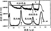
Si-O+F→Si-F+O+1.1eV (1)Si-O+F→Si-F+O+1.1eV (1)
这一改性结构有助于杂质较高的扩散速度和提高的湿气吸收。此外,公知当氟化二氧化硅(SiOF)暴露于潮湿氛围下时,它有效地吸收水。V.Pankov,J.C.Alonso和A.Ortiz,J.Appl.Phys.86(1999),p.275(其全文内容在此通过参考引入)。This modified structure contributes to a higher diffusion rate of impurities and increased moisture absorption. Furthermore, it is known that fluorinated silicon dioxide (SiOF) absorbs water efficiently when it is exposed to a humid atmosphere. V. Pankov, J. C. Alonso and A. Ortiz, J. Appl. Phys. 86 (1999), p. 275 (the entire content of which is hereby incorporated by reference).
在HF浸渍,如在本发明的0.025%HF水溶液中浸渍的过程中,除了在二氧化硅表面上形成Si-F和Si-OH基以外,还如下所述生成一些F离子:During HF impregnation, such as in the 0.025% HF aqueous solution of the present invention, in addition to the formation of Si-F and Si-OH groups on the silica surface, some F ions are generated as follows:
2HF+H2O←→H3O++HF2-2HF+H2 O←→H3 O+ +HF2-
Si-OH+HF2-→Si-F+F-+H2O (2)Si-OH+HF2- → Si-F+F- +H2 O (2)
参见,例如H.Nielsen和D.Hackleman,J.Electrochem.Soc.Vol.130(1983)p.708(其全文内容在此通过参考引入)。在升高的温度下后HF烘烤有助于除去通过上述反应生成的水并提高氟的扩散。氟原子扩散到氧化物内,并根据方程式(1)与Si-O-Si键反应,形成SiOF。See, eg, H. Nielsen and D. Hackleman, J. Electrochem. Soc. Vol. 130 (1983) p. 708 (the entire contents of which are hereby incorporated by reference). The post HF bake at elevated temperature helps to remove the water formed by the above reaction and enhances the diffusion of fluorine. Fluorine atoms diffuse into the oxide and react with Si-O-Si bonds according to equation (1) to form SiOF.
较高温度的后HF烘烤可在氧化物表面上产生较厚的SiOF层,由于较高效率的吸水从而导致较高的室温粘结能。然而,对于最多350℃的烘烤来说,图6的结果表明,当后HF烘烤温度高于300℃时,所得粘结能实际上低于在较低温度下的烘烤。Chang等,Appl.Phys.Lett.vol.69(1996)p.1238(其全文内容在此通过参考引入)报道了若SiOF沉积温度高于300℃,则由于在氧化物内氟原子的损失导致该层的耐湿性开始增加。因此,对于在粘结之前,在350℃下后HF退火的晶片对来说,室温粘结能的下降可归因于下述事实:在粘结界面处的SiOF层吸收的湿气小于250℃退火的层,尽管SiOF层可能较厚。A higher temperature post HF bake can produce a thicker SiOF layer on the oxide surface, resulting in a higher room temperature adhesion energy due to a higher efficiency of water absorption. However, for bakes up to 350°C, the results in Figure 6 show that when the post HF bake temperature is higher than 300°C, the resulting bond energy is actually lower than for bakes at lower temperatures. Chang et al., Appl. Phys. Lett. vol. 69 (1996) p. 1238 (the entire content of which is hereby incorporated by reference) reported that if the SiOF deposition temperature is higher than 300 ° C, due to the loss of fluorine atoms in the oxide leads to The moisture resistance of this layer starts to increase. Therefore, for wafer pairs post-HF annealed at 350 °C before bonding, the decrease in room temperature bonding energy can be attributed to the fact that the SiOF layer at the bonding interface absorbs less moisture than 250 °C annealed layer, although the SiOF layer may be thicker.
在本发明的优选工艺中,根据下述交换反应,二氧化硅的最外层的表面终止从后HF退火的Si-F转化成RCA1溶液清洗之后的Si-OH:In a preferred process of the present invention, the surface of the outermost layer of silica is terminated from Si-F after HF annealing to Si-OH after RCA1 solution cleaning according to the following exchange reaction:
Si-F+HOH→Si-OH+HF (3)Si-F+HOH→Si-OH+HF (3)
在例如含水NH4OH浸渍(含有约65%的H2O)之后,大多数Si-OH基然后转化成Si-NH2:After e.g. aqueous NH4 OH impregnation (containing about 65% H2 O), most of the Si-OH groups are then converted to Si-NH2 :
Si-OH+NH4OH→Si-NH2+2HOH (4)Si-OH+NH4 OH→Si-NH2 +2HOH (4)
然而,在NH4OH浸渍之后,由于在NH4OH内的H2O含量导致表面仍部分OH基终止。However, after NH4 OH impregnation, the surface is still partially terminated with OH groups due to the H2 O content in NH4 OH.
Si-NH2和Si-OH终止的表面在室温下粘结,且当两种表面足够接近时,发生下述反应:Si-NH2 and Si-OH terminated surfaces bond at room temperature, and when the two surfaces are sufficiently close, the following reaction occurs:
Si-NH2+Si-NH2←→Si-N-N-Si+H2 (5)Si-NH2 +Si-NH2 ←→Si-NN-Si+H2 (5)
Si-OH+HO-Si←→Si-O-Si+HOH (6)Si-OH+HO-Si←→Si-O-Si+HOH (6)
例如,Q.-Y.Tong和U.Goesele,J.Electroch.Soc.,142(1995),p.3975报道了可在室温下,在氢键键合到相反键合的亲水表面上的两个Si-OH之间形成Si-O-Si共价键。然而,上述聚合反应在小于~425℃的温度下是可逆的。参见,例如M.L.Hair,in SiliconChemistry,E.R.Corey,J.Y.Corey和P.P.Gaspar,Eds.,Wiley,NewYork(1987),p.482(其全文内容在此通过参考引入)。For example, Q.-Y.Tong and U.Goesele, J.Electroch.Soc., 142 (1995), p.3975 reported that at room temperature, hydrogen bonding to the opposite bonding hydrophilic surface A Si-O-Si covalent bond is formed between two Si-OH. However, the above polymerization reaction is reversible at temperatures less than ~425°C. See, eg, M.L. Hair, in Silicon Chemistry, E.R. Corey, J.Y. Corey and P.P. Gaspar, Eds., Wiley, New York (1987), p. 482 (the entire contents of which are hereby incorporated by reference).
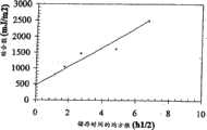
若可在没有加热的情况下,除去通过上述反应生成的水和氢气,则根据上述反应,共价键不具有可逆性,且导致室温下永久的共价键合。根据本发明,通过在粘结之前,氟化氧化物,在远离粘结表面处氟掺入到氧化物内,且上述聚合反应的副产物可通过从粘结界面扩散到远离粘结界面的低密度的氟化氧化物内,从而导致在室温下在界面处高度的共价键合。图7示出了对于使用与第II组中的那些相同的工艺条件下,在室温下粘结的氧化物覆盖的晶片对来说,在室温下,作为储存时间的均方根函数的粘结能。对于水的恒定总量S来说,在粘结界面Cs1处的水浓度与均方根时间t和水的扩散系数D1成反比,和在粘结界面处的氢气浓度Cs2与均方根时间t和氢气的扩散系数D2成反比:If the water and hydrogen generated by the above reaction can be removed without heating, the covalent bond is not reversible according to the above reaction and leads to a permanent covalent bond at room temperature. According to the present invention, by fluorinating the oxide prior to bonding, fluorine is incorporated into the oxide at a location remote from the bonding surface, and the by-products of the above-mentioned polymerization reactions can be obtained by diffusing from the bonding interface to a low temperature remote from the bonding interface. density within the fluorinated oxide, resulting in a high degree of covalent bonding at the interface at room temperature. Figure 7 shows the bonding as a function of root mean square of storage time at room temperature for pairs of oxide-covered wafers bonded at room temperature using the same process conditions as those in Group II. able. For a constant total amount of water S, the water concentration at the bonding interface Cs1 is inversely proportional to the root mean square time t and the water diffusion coefficient D1 , and the hydrogen concentration at the bonding interface Cs2 is proportional to the mean square The root time t is inversely proportional to the diffusion coefficient D2 of hydrogen:
Cs1=S(πD1t)1/2 (7.1)Cs1 = S(πD1 t)1/2 (7.1)
Cs2=S(πD2t)1/2 (7.2)Cs2 =S(πD2 t)1/2 (7.2)
参见,例如J.C.C.Tsai,VLSI Technology,S.M.Sze,Ed.,McGraw-Hill,Auckland,(1983),p.147(其全文内容在此通过参考引入)。See, eg, J.C.C. Tsai, VLSI Technology, S.M. Sze, Ed., McGraw-Hill, Auckland, (1983), p. 147 (the entire contents of which are hereby incorporated by reference).
当在粘结界面处,粘结能γ与水和氢气浓度成反比时,粘结能应当与氢气和水浓度的倒数成正比:While the bond energy γ is inversely proportional to the water and hydrogen concentrations at the bonding interface, the bond energy should be proportional to the reciprocal of the hydrogen and water concentrations:
γ~(Cs1+Cs2)-1 (8)γ~(Cs1 +Cs2 )-1 (8)
尽管NH2终止的浓度可大于OH终止浓度,从而导致在粘结之后H2浓度比H2O高,但认为氢气的扩散性显著高于水,这是因为其尺寸小得多(2.5埃相对于3.3埃)。粘结能的增加可能主要由水的扩散支配,且如果扩散系数恒定,则与时间的均方根成正比:Although the concentration ofNH2 termination can be greater than that of OH termination, resulting in a higher concentration ofH2 thanH2O after bonding, it is believed that hydrogen gas is significantly more diffusible than water due to its much smaller size (2.5 Å vs. at 3.3 Angstroms). The increase in bonding energy is likely to be dominated by the diffusion of water and, if the diffusion coefficient is constant, is proportional to the root mean square of time:
γ~1/Cs1=(πD1t)1/2/S (9)γ~1/Cs1 =(πD1 t)1/2 /S (9)
与这一结论一致的是,如图7所示,观察到所测量的粘结能与时间的均方根之间接近线性的关系,这与水(和氢气)扩散远离粘结界面进入氟化氧化物层内一致。因此,水(和氢气)扩散远离粘结界面可能是在本发明中观察到的粘结能提高的原因,但本发明不限于导致水副产物的反应和所述水(和氢气)副产物扩散远离所述粘结表面。Consistent with this conclusion, as shown in Fig. 7, a nearly linear relationship is observed between the measured bonding energy and the root mean square of time, which is consistent with the diffusion of water (and hydrogen) away from the bonding interface into the fluorinated Consistent within the oxide layer. Therefore, diffusion of water (and hydrogen) away from the bonding interface may be responsible for the increase in bond energy observed in the present invention, but the invention is not limited to reactions leading to water by-products and diffusion of said water (and hydrogen) by-products away from the bonding surface.
对于主要用OH基终止的粘结表面,例如与第IV组内的晶片一样的没有用NH4OH处理的粘结表面来说,存在显著较高浓度的水扩散离开该界面。因此,用NH4OH浸渍的晶片对的粘结能随储存时间快速增加,且与图5所示的不用NH4OH浸渍处理的晶片对相比,达到高得多的数值。For bonding surfaces that are primarily terminated with OH groups, such as those not treated withNH4OH like the wafers in Group IV, there is a significantly higher concentration of water diffusing away from the interface. Consequently, the bonding energy of wafer pairs impregnated withNH4OH increased rapidly with storage time and reached much higher values compared to the wafer pairs not treated withNH4OH impregnation as shown in FIG. 5 .
图8A-8C示出了在随后的粘结中使用的氟化氧化物层的方法。在于待粘结的基底90上形成氧化物层81(图9A)之后,或者通过湿法或者通过气体法,将氧化物暴露于HF下。气体工艺的实例是没有在HF溶液中浸渍的情况下,将晶片表面暴露于HF蒸汽下,可以以许多方式形成氧化物,其中包括,但不限于,溅射、等离子加强的气相沉积(PECVD)和热生长。基底可以是有或无在其内形成的器件的硅片。或者,F可以采用20-30keV的能量,通过1×10¹⁵到1×10¹⁶/cm2的氟离子植入,从而引入到氧化物层内。Figures 8A-8C illustrate the method of fluorinating the oxide layer used in subsequent bonding. After forming the oxide layer 81 (FIG. 9A) on the
在于~250℃下退火之后,在层81的表面82内形成厚度约0.5微米的SiOF表面粘结层83(图8B)。注意,层83的尺寸没有按比例画出。基底备用于粘结到具有第二粘结层85(其也具有在表面内形成的SiOF层86)的另一基底84上,粘结能在环境中,在室温下进行,如图8C所示。在室温下在基底之间形成非常高密度的共价粘结,其比没有使用HF浸渍和烘烤的晶片对高最多2.5倍(通过所测量的粘结强度来推导)。After annealing at -250°C, a SiOF
还可将SiOF表面层粘结到不具有SiOF表面层的另一粘结层上。还可通过F+植入和/或蚀刻(例如,使用SF6和/或CF4的干燥蚀刻)氧化硅,接着在升高的温度下烘烤,形成SiOF表面层。另外,可通过PECVD(等离子加强的化学气相沉积)形成SiOF表面层。例如,在室温下,电子-共振PECVD氧化物沉积使用SiF4/Ar/N2O(S.P.Kim,S.K.Choi,Y.Park和I Chung,Appl.Phys.Lett.79(2001),p.185,PECVD oxide deposition using Si2H6/CF4/N2O at 120℃,J.Song,P.K.Ajmera和G.S.Lee,Appl.Phys.Lett.69(1996),p.1876or SiF4/O2/Ar at 300℃ S.Lee和J.Park,Appl.Phys.Lett.80(1996),p.5260)。It is also possible to bond the SiOF surface layer to another bonding layer which does not have a SiOF surface layer. The SiOF surface layer can also be formed by F+ implantation and/or etching (eg, dry etching using SF6 and/or CF4 ) of silicon oxide, followed by baking at elevated temperature. In addition, the SiOF surface layer may be formed by PECVD (Plasma Enhanced Chemical Vapor Deposition). For example, at room temperature, electron-resonant PECVD oxide deposition uses SiF4 /Ar/N2 O (SP Kim, SK Choi, Y. Park and I Chung, Appl. Phys. Lett. 79 (2001), p.185, PECVD oxide deposition using Si2 H6 /CF4 /N2 O at 120°C, J.Song, PKAjmera and GS Lee, Appl.Phys.Lett.69(1996), p.1876or SiF4 /O2 /Ar at 300°C S. Lee and J. Park, Appl. Phys. Lett. 80 (1996), p. 5260).
HF浸渍和退火,以便在二氧化硅表面上形成SiOF表面粘结层具有独特的应用。图9A-E图示了可使用本发明生产局部变化的共价粘结,和因此局部变化的在表面上的粘结能。图9A示出了在硅片上,在暴露的二氧化硅的选择区域内,在此情况下,硅器件区域内,使用稀释的HF(或缓冲的HF)溶液,从表面上蚀刻掉小量的氧化物。基底90具有二氧化硅层91和器件部分92。器件部分可以是离散的器件,电路或者集成电路。在具有孔隙94的氧化物91上形成光致抗蚀剂或掩膜层93。稀释的HF溶液蚀刻通过孔隙94暴露的二氧化硅,生成下凹的区域95。下凹的区域可具有非常宽范围的深度,从数纳米到许多微米,但较厚的吹塑也是可能的(图9B)。光致抗蚀剂或者掩膜层抗HF蚀刻。除去层93,接着如图9C所示,在~250℃下在整个表面上沉积二氧化硅。250℃再沉积工艺模拟后HF烘烤处理的效果且包埋稀释的HF处理过的表面。HF dipping and annealing to form a SiOF surface bonding layer on a SiO2 surface has unique applications. Figures 9A-E illustrate that locally varying covalent bonds, and thus locally varying bonding energies on surfaces, can be produced using the present invention. Figure 9A shows that on a silicon wafer, in selected areas of exposed silicon dioxide, in this case, the silicon device area, a small amount is etched away from the surface using a dilute HF (or buffered HF) solution. of oxides.
CMP工艺步骤然后可用于平面化下凹的区域并改进表面粗糙度。第I组表面处理然后用到层96上,和硅片在室温下粘结到另一晶片,例如覆盖晶片98的二氧化硅层97上,如图9D所示。沿着本发明的粘结界面,在HF的蚀刻区域内,室温粘结能显著高于非HF蚀刻的区域。A CMP process step can then be used to planarize the recessed areas and improve surface roughness. Group I surface treatment is then applied to
当如此形成的粘结对被迫分离时,所得分离典型地不在HF浸渍的器件区域的粘结界面处。确实,一部分硅片或者硅片本身可在粘结界面下方处断裂并从基底上剥离,如图9D所图示。基底90的部分99连接到器件或电路92上。层91的部分100和层96的部分101因断裂而分离(图9E)。When a bonded pair so formed is forced to separate, the resulting separation is typically not at the bond interface of the HF impregnated device region. Indeed, a portion of the wafer, or the wafer itself, may fracture below the bonding interface and peel off the substrate, as illustrated in Figure 9D.
在图10的显微照片中示出了图9图示的实际实例,其表明,来自粘结对的晶片残余物被迫分离。这一残余物表明在其中表面暴露于HF下的粘结界面下方硅片内的断面。这与在这些位置内氧化硅层之间的粘结能高于本体硅的断裂能一致。在晶片对的粘结界面的其它位置上,同样如图10所示,表面没有暴露于HF下。在这些位置内,认为粘结能低于本体硅的断裂能。这与在这些区域内缺少硅的剥离一致。A practical example of the diagram illustrated in FIG. 9 is shown in the photomicrograph of FIG. 10, which shows that the wafer residue from the bonded pair is forced to separate. This residue indicated a fracture in the silicon wafer below the bonding interface where the surface was exposed to HF. This is consistent with the higher bonding energy between silicon oxide layers than the fracture energy of bulk silicon in these locations. At other locations on the bonding interface of the wafer pair, as also shown in Figure 10, the surfaces were not exposed to HF. Within these locations, the bonding energy is believed to be lower than the fracture energy of bulk silicon. This is consistent with the absence of silicon exfoliation in these regions.
这种局部的氟化由于将F引入到氧化物内,降低该材料的介电常数,也可导致形成较低k的电介质。可利用本发明的这一特征,在集成电路或其它结构体的设计中发挥优势。例如,可在VLSI器件内,在金属线之间,而不是在多层互连体的通路电平内,通过蚀刻工艺,例如暴露于HF下,在其中希望低k电介质的区域内,形成低k电介质,接着在~250℃下沉积氧化物。图11示出了包埋的低k结构体的一个实例。在图11中,在氧化物层,例如SiO2,110、112和114之间形成低k材料层部分111和113。金属层115和117通过通路116和118连接。This localized fluorination can also lead to the formation of lower k dielectrics by introducing F into the oxide, lowering the dielectric constant of the material. This feature of the invention can be used to advantage in the design of integrated circuits or other structures. For example, in VLSI devices, low-k dielectrics can be formed in regions where low-k dielectrics are desired, between metal lines, rather than within the via level of a multilayer interconnect, by an etch process, such as exposure to HF. dielectric, followed by oxide deposition at ~250°C. Figure 11 shows an example of an embedded low-k structure. In FIG. 11 , low-k
实施例Example
使用图8A-8C再次描述本发明方法的第二个实施例。在基底80上形成第一氧化物层81(图8A)。通过以上所述的工序之一,亦即,暴露于HF下或者暴露于含氟气体下,将氟引入到膜81内。例如,在膜81上通过PECVD形成第二氧化物膜82(图8B)。也可通过使用沉积所述氧化物膜82用的合适的含氟前体,将它引入到第二膜内。注意,在该实施例中,膜81和82的尺寸没有按比例画出,这是因为该附图还用于描述其中在膜81内形成膜82的实施例,但该附图确实准确地代表了膜81和82的位置。在该实施例中,由于沉积温度和/或与所述氧化物膜82有关的含氟前体导致不需要烘烤基底,以生成辅助除去反应副产物的氟化层。然后将该用品备用于粘结另一晶片,如图8C所示。The second embodiment of the method of the present invention is described again using Figs. 8A-8C. A
在图10所示的样品上,在其中形成氧化硅层,并暴露于HF溶液,接着在250℃下沉积氧化物这样处理的样品的HF暴露表面积内,进行SIMS(次级离子质谱)测量。然后将该样品浸渍在NH4OH溶液内。图12示出了测量结果。图12所示的SIMS测量结果证明在粘结之前在NH4OH内浸渍的粘结晶片的粘结界面处Si-N共价键的存在。此外,SIMS断面测量清楚地证明在氧化物沉积的界面附近,在HF蚀刻的凹处存在高的氟浓度。由于在氧化物沉积之前,该样品仅仅暴露于HF下,因此合理地将在粘结界面处的F信号归因于F通过沉积的氧化物扩散并在250℃氧化物沉积过程中在氧化物表面处累积。在粘结界面处的氟浓度为约2×10¹⁸/cm3,和峰值氮浓度为~3.5×1020/cm3。远离粘结界面处的F有助于除去反应副产物,例如HOH,从而导致增加浓度的永久共价键和粘结强度。SIMS (Secondary Ion Mass Spectrometry) measurement was performed on the sample shown in FIG. 10 within the HF exposed surface area of the sample treated by forming a silicon oxide layer therein and exposing to an HF solution followed by depositing an oxide at 250°C. The sample was then immersed inNH4OH solution. Fig. 12 shows the measurement results. The SIMS measurements shown in Figure 12 demonstrate the presence of Si-N covalent bonds at the bonding interface of bonded wafers dipped inNH4OH prior to bonding. Furthermore, SIMS cross-sectional measurements clearly demonstrate the presence of high fluorine concentrations in the HF-etched recesses near the oxide-deposited interface. Since this sample was only exposed to HF prior to oxide deposition, it is reasonable to attribute the F signal at the bonding interface to the diffusion of F through the deposited oxide and on the oxide surface during oxide deposition at 250 °C. accumulated. The fluorine concentration at the bond interface was about 2×10¹⁸ /cm3 , and the peak nitrogen concentration was ~3.5×10²⁰ /cm3 . F away from the bonding interface facilitates the removal of reaction by-products, such as HOH, leading to an increased concentration of permanent covalent bonds and bond strength.
在250℃下后HF含水浸渍烘烤10小时可与反复PECVD氧化物沉积的温度与持续时间相当。因此在HF浸渍之后,通过在HF处理的表面上沉积PECVD氧化物,可避免独立的退火步骤。这一优点的实例是在晶片粘结的制备中,在非平面晶片的平面化中。例如,对于集成电路(IC)的粘结来说,室温粘结可能非常有用。然而,IC典型地具有非平面表面,这不利于对于室温直接晶片粘结来说优选的平坦和光滑表面。改进这一平坦度的方法是沉积氧化物层,接着CMP。这类似于以上提供的实施例,所不同的是,非平坦度可以是1微米或者更大。在非平坦度增加的这一情况下,沉积较厚的氧化物或者大于一次地反复沉积氧化物,并使用CMP实现所需的平坦度。在这一平面化工艺中,若在(最后)的氧化物沉积之前,采用HF处理,则随后的氧化物沉积将具有增加的F浓度,和在氧化物沉积之后在其表面处具有F的累积。与若不使用HF处理所获得的粘结能相比,例如如上所述,采用第I组预粘结处理,且没有任何后氧化物生长热处理的情况下,这一F浓度可导致较高的粘结能。A post-HF aqueous dip bake at 250°C for 10 hours is comparable to the temperature and duration of repeated PECVD oxide deposition. A separate annealing step can thus be avoided by depositing PECVD oxide on the HF treated surface after HF dipping. Examples of this advantage are in the preparation of wafer bonding, in the planarization of non-planar wafers. For example, for the bonding of integrated circuits (ICs), room temperature bonding can be very useful. However, ICs typically have non-planar surfaces, which is detrimental to the flat and smooth surfaces that are preferred for room temperature direct wafer bonding. A way to improve this flatness is to deposit an oxide layer followed by CMP. This is similar to the example provided above, except that the non-flatness can be 1 micron or greater. In this case of increased non-planarity, deposit thicker oxide or repeatedly deposit oxide more than once and use CMP to achieve the desired planarity. In this planarization process, if HF treatment is applied before the (final) oxide deposition, the subsequent oxide deposition will have an increased F concentration and a buildup of F at its surface after the oxide deposition . This F concentration results in a higher bond energy than would be obtained if no HF treatment was used, e.g., with Group I pre-bond treatment, as described above, without any post-oxide growth heat treatment. bonding energy.
可在环境条件下,而不是限制到高或超高真空(UHV)条件下,进行本发明的方法。因此,本发明的方法是成本低,可批量生产的制造技术。该方法也不限于晶片的类型、待粘结的基底或元件。晶片可以是本体材料,例如硅,具有在其内形成的器件的晶片,处理器基底、散热片等。The methods of the invention can be carried out under ambient conditions, not limited to high or ultra high vacuum (UHV) conditions. Therefore, the method of the present invention is a low-cost, mass-producible manufacturing technique. The method is also not limited to the type of wafer, substrate or components to be bonded. A wafer may be a bulk material, such as silicon, a wafer with devices formed therein, a processor substrate, a heat sink, and the like.
尽管图2A和2B示出了粘结在一起的两种器件,但该方法不限于粘结两种器件。可除去基底200和203之一并反复处理,正如图2C和2D所示。在图2C中,通过包括粉碎、搭接、抛光和化学蚀刻中的一种或多种工艺在内的工序,对图2B所示结构的基底203进行基底除去,得到部分207。可基于进行该方法的材料或者结构体的类型决定合适的一种或多种方法。在其中基底203在其表面上含有器件或其它元件的情况下,除了其中器件或其它元件驻留的区域以外,可除去所有或基本上所有的基底203。基于材料、材料的蚀刻特征或者特定应用的细节,可改变除去的量。Although Figures 2A and 2B illustrate two devices bonded together, the method is not limited to bonding two devices. One of the
在部分207(如图2C所示)上形成相同或者不同材料的另一粘结层208,例如沉积的氧化硅材料,和如上所述制备具有粘结层2-7的基底209,亦即,使层210的表面变光滑到以上所述范围内的表面粗糙度,并以与以上所述相同的方式在界面211处,粘结到层108上。图2D示出了所得结构体。该工艺可进行N次,视需要产生(N+1)集成结构体。Another bonding layer 208 of the same or a different material is formed on portion 207 (as shown in FIG. 2C ), such as a deposited silicon oxide material, and
本发明可局部粘结到全部晶片表面积上或者可粘结在整个全部晶片表面积上。换句话说,较小的小片可粘结到较大的小片上。这在图13中示出,其中具有相应粘结层134、136和138的数个较小的小片133、135和137粘结到粘结层131的表面132上。The present invention may be bonded locally to the entire wafer surface area or may be bonded to the entire wafer surface area. In other words, smaller dies can be bonded to larger dies. This is shown in FIG. 13 , where several
本发明还可用于室温金属的直接粘结,正如在申请序列号10/359608中所述(其内容在此通过参考引入)。正如图14A所示,两个基底140和143具有各自的粘结层141和144以及金属垫142和145。间隙146隔开垫片,和垫片的上表面在层141和144的上表面上延伸。制备层141和144的表面以供如上所述的粘结,然后使基底的金属垫片接触(图14B)。至少一个基底弹性变形,且粘结层141和144接触,并开始在层141和144之间的一个或多个点处粘结(图14C)。粘结生长形成粘结体147。在室温下,形成强的粘结(例如共价粘结)。The present invention may also be used for direct bonding of room temperature metals as described in Application Serial No. 10/359608 (the contents of which are incorporated herein by reference). As shown in FIG. 14A , two
图15示出了较小的器件或小片151和152对较大基底150的金属粘结。在器件151和152内的结构体153和154分别可以是有源器件或者接触结构体。在基底150内,还可以是有源器件或者含有有源器件的结构体156,具有接触结构体155。在基底150上的粘结层157和在较小器件151和152上的粘结层158之间的界面159处形成粘结。FIG. 15 shows the metal bonding of smaller devices or dies 151 and 152 to a
金属直接粘结提供许多优点,其中包括省去磨光(grinding)和修磨小片,藉助蚀刻和金属沉积形成电连接,如参考的现有技术中所述一样互连相连的晶片。这消除了因这些小片磨光和修磨而引起的任何机械破坏。此外,省去深的通路蚀刻避免了台阶式覆盖问题,使得该方法可按比例缩小到较小尺寸,从而导致较小的通路插塞(plug)接触粘结的晶片。该方法与其它标准的半导体工艺兼容,且与VLSI兼容。Metal direct bonding offers many advantages, including eliminating the need for grinding and trimming the die, forming electrical connections by means of etching and metal deposition, and interconnecting connected wafers as described in the referenced prior art. This eliminates any mechanical damage caused by lapping and dressing of these small pieces. Furthermore, the elimination of deep via etch avoids the step coverage problem, making the method scalable to smaller dimensions, resulting in smaller via plug contact bonded wafers. The method is compatible with other standard semiconductor processes and compatible with VLSI.
在进一步的实施例中,本发明的方法可用于气密封装,如图16A-16E所示。在载体上形成氟化的粘结层162,并在形成器件161,例如MEMS的过程中受到保护。图16A示出了在载体160上形成粘结层162,接着在粘结层162上形成保护膜163,和在载体160上形成器件161的步骤。作为实例,载体160可以是硅基底,和粘结层162可以是具有合适的表面粗糙度和平坦度特征的沉积的氧化物层,以促进室温粘结。如图16B所示,在形成器件161之后除去膜163,和在将粘结层162粘结到表面164上的位置处,制备具有合适的表面粗糙度和平坦度特征的覆盖层165,所述覆盖层165具有带表面167的部分166。使表面167与表面164直接接触并粘结,形成粘结体169,如图16C所示。图16D代表图16A-16C所示的方法的改性,其中在部分166上形成具有合适的表面和平坦度特征的粘结层170。使膜170的表面与膜162的表面接触并粘结,形成粘结体171。图16E示出了图16A-16C所示的方法的另一改性,其中覆盖层由板172和在该板172上形成的部分173组成。如上所述制备部分173的表面,并粘结162形成粘结体174。图16E的右手部分示出了进一步的改性,其中采用膜174,将部分173粘结到板172上,并粘结到层162上,形成粘结体175。在任何一种情况下,部分173可以是氧化物或硅材料,和板172可以是硅板。In a further embodiment, the method of the present invention can be used in hermetic packaging, as shown in Figures 16A-16E. A
根据本发明,通过任何方法,例如沉积、溅射、热或化学氧化,和玻璃上旋涂形成的二氧化硅可以以纯或者掺杂的状态使用。According to the invention, silicon dioxide formed by any method, such as deposition, sputtering, thermal or chemical oxidation, and spin coating on glass, can be used in pure or doped state.
在本发明的优选实施方案中,在水化之后和在粘结之前,通过氟化表面二氧化硅层覆盖的晶片的氨水溶液浸渍显著增加室温粘结能,这是由于形成Si-N键和氢键所致。In a preferred embodiment of the invention, after hydration and before bonding, immersion in ammonia solution by fluorinated surface silica layer-covered wafers significantly increases room temperature bonding energy due to the formation of Si-N bonds and due to hydrogen bonding.
HF-浸渍和后HF烘烤可在晶片上的所需位置处,例如在二氧化硅层内的蚀刻窗处产生局部的共价键合。或者F的植入和随后退火可在所需位置处产生局部的共价键合。HF-dipping and post HF-baking can produce localized covalent bonding at desired locations on the wafer, for example at etched windows in a silicon dioxide layer. Alternatively implantation of F and subsequent annealing can produce localized covalent bonding at desired locations.
根据本发明,HF-浸渍和后HF烘烤可在二氧化硅层内局部形成低k电介质。例如,可在VLSI器件内,在多层互连体内的金属线之间,但不是在通路电平处形成低k电介质。According to the present invention, HF-dipping and post HF-baking can locally form a low-k dielectric within the silicon dioxide layer. For example, in VLSI devices, low-k dielectrics can be formed between metal lines within a multilayer interconnect, but not at via levels.
本发明的方法可用于任何类型的基底,例如散热片、处理器或代用基底,具有有源器件的基底,具有集成电路的基底等。不同技术的基底,即硅、III-V材料,II-VI材料等可在本发明中使用。The method of the present invention can be used on any type of substrate, such as heat sinks, processor or surrogate substrates, substrates with active devices, substrates with integrated circuits, etc. Substrates of different technologies, ie silicon, III-V materials, II-VI materials, etc. can be used in the present invention.
本发明的应用包括,但不限于,用于3-D SOC的加工集成电路的垂直整合,微垫片封装、倒装片结合的低成本和高性能替代品,晶片级封装,热处理和独特的器件结构体,如金属基础器件。Applications of the present invention include, but are not limited to, vertical integration of processed integrated circuits for 3-D SOCs, low-cost and high-performance alternatives to micro-shim packaging, flip-chip bonding, wafer-level packaging, thermal processing and unique Device structures, such as metal-based devices.
鉴于上述教导,本发明的许多改性和改变是可能的。因此,要理解,可在此处具体地所述的以外在所附权利要求的范围内实践本发明。Many modifications and variations of the present invention are possible in light of the above teachings. It is therefore to be understood that within the scope of the appended claims the invention may be practiced other than as specifically described herein.
Claims (9)
Applications Claiming Priority (2)
| Application Number | Priority Date | Filing Date | Title |
|---|---|---|---|
| US10/440,099US7109092B2 (en) | 2003-05-19 | 2003-05-19 | Method of room temperature covalent bonding |
| US10/440,099 | 2003-05-19 |
Related Parent Applications (1)
| Application Number | Title | Priority Date | Filing Date |
|---|---|---|---|
| CNB2004800181251ADivisionCN100468639C (en) | 2003-05-19 | 2004-05-19 | Room temperature covalent bonding method |
Publications (2)
| Publication Number | Publication Date |
|---|---|
| CN101359605Atrue CN101359605A (en) | 2009-02-04 |
| CN101359605B CN101359605B (en) | 2010-10-13 |
Family
ID=33449761
Family Applications (2)
| Application Number | Title | Priority Date | Filing Date |
|---|---|---|---|
| CNB2004800181251AExpired - LifetimeCN100468639C (en) | 2003-05-19 | 2004-05-19 | Room temperature covalent bonding method |
| CN2008101340522AExpired - LifetimeCN101359605B (en) | 2003-05-19 | 2004-05-19 | Method of room temperature covalent bonding |
Family Applications Before (1)
| Application Number | Title | Priority Date | Filing Date |
|---|---|---|---|
| CNB2004800181251AExpired - LifetimeCN100468639C (en) | 2003-05-19 | 2004-05-19 | Room temperature covalent bonding method |
Country Status (9)
| Country | Link |
|---|---|
| US (8) | US7109092B2 (en) |
| EP (1) | EP1631981A4 (en) |
| JP (2) | JP5570680B2 (en) |
| KR (1) | KR101154227B1 (en) |
| CN (2) | CN100468639C (en) |
| CA (1) | CA2526481A1 (en) |
| IL (2) | IL171996A0 (en) |
| SG (1) | SG185826A1 (en) |
| WO (1) | WO2004105084A2 (en) |
Cited By (2)
| Publication number | Priority date | Publication date | Assignee | Title |
|---|---|---|---|---|
| CN102376653A (en)* | 2010-08-20 | 2012-03-14 | S.O.I.Tec绝缘体上硅技术公司 | low temperature bonding method |
| CN112216642A (en)* | 2019-07-09 | 2021-01-12 | 美科米尚技术有限公司 | Liquid-assisted bonding method |
Families Citing this family (390)
| Publication number | Priority date | Publication date | Assignee | Title |
|---|---|---|---|---|
| US8058142B2 (en)* | 1996-11-04 | 2011-11-15 | Besang Inc. | Bonded semiconductor structure and method of making the same |
| US8018058B2 (en)* | 2004-06-21 | 2011-09-13 | Besang Inc. | Semiconductor memory device |
| US7470142B2 (en)* | 2004-06-21 | 2008-12-30 | Sang-Yun Lee | Wafer bonding method |
| FR2773261B1 (en) | 1997-12-30 | 2000-01-28 | Commissariat Energie Atomique | METHOD FOR THE TRANSFER OF A THIN FILM COMPRISING A STEP OF CREATING INCLUSIONS |
| US6984571B1 (en) | 1999-10-01 | 2006-01-10 | Ziptronix, Inc. | Three dimensional device integration method and integrated device |
| US6902987B1 (en) | 2000-02-16 | 2005-06-07 | Ziptronix, Inc. | Method for low temperature bonding and bonded structure |
| US6962835B2 (en) | 2003-02-07 | 2005-11-08 | Ziptronix, Inc. | Method for room temperature metal direct bonding |
| US7109092B2 (en) | 2003-05-19 | 2006-09-19 | Ziptronix, Inc. | Method of room temperature covalent bonding |
| US8071438B2 (en) | 2003-06-24 | 2011-12-06 | Besang Inc. | Semiconductor circuit |
| DE102004060364A1 (en)* | 2004-12-15 | 2006-06-29 | Austriamicrosystems Ag | Semiconductor substrate with multilayer structure and method for the production |
| US8367524B2 (en) | 2005-03-29 | 2013-02-05 | Sang-Yun Lee | Three-dimensional integrated circuit structure |
| US7485968B2 (en) | 2005-08-11 | 2009-02-03 | Ziptronix, Inc. | 3D IC method and device |
| FR2889887B1 (en) | 2005-08-16 | 2007-11-09 | Commissariat Energie Atomique | METHOD FOR DEFERING A THIN LAYER ON A SUPPORT |
| FR2891281B1 (en)* | 2005-09-28 | 2007-12-28 | Commissariat Energie Atomique | METHOD FOR MANUFACTURING A THIN FILM ELEMENT |
| FR2910179B1 (en) | 2006-12-19 | 2009-03-13 | Commissariat Energie Atomique | METHOD FOR MANUFACTURING THIN LAYERS OF GaN BY IMPLANTATION AND RECYCLING OF A STARTING SUBSTRATE |
| US7812459B2 (en)* | 2006-12-19 | 2010-10-12 | Taiwan Semiconductor Manufacturing Company, Ltd. | Three-dimensional integrated circuits with protection layers |
| JP2009016393A (en)* | 2007-06-29 | 2009-01-22 | Toshiba Corp | Semiconductor substrate, semiconductor device, and method of manufacturing semiconductor substrate |
| JP5452900B2 (en)* | 2007-09-21 | 2014-03-26 | 株式会社半導体エネルギー研究所 | Method for manufacturing substrate with semiconductor film |
| FR2922359B1 (en)* | 2007-10-12 | 2009-12-18 | Commissariat Energie Atomique | METHOD FOR MANUFACTURING A MICROELECTRONIC STRUCTURE INVOLVING MOLECULAR COLLAGE |
| JP4348454B2 (en)* | 2007-11-08 | 2009-10-21 | 三菱重工業株式会社 | Device and device manufacturing method |
| US8119490B2 (en)* | 2008-02-04 | 2012-02-21 | Semiconductor Energy Laboratory Co., Ltd. | Method for manufacturing SOI substrate |
| US8017451B2 (en) | 2008-04-04 | 2011-09-13 | The Charles Stark Draper Laboratory, Inc. | Electronic modules and methods for forming the same |
| US8273603B2 (en) | 2008-04-04 | 2012-09-25 | The Charles Stark Draper Laboratory, Inc. | Interposers, electronic modules, and methods for forming the same |
| US8459779B2 (en) | 2008-04-11 | 2013-06-11 | Lexmark International, Inc. | Heater chips with silicon die bonded on silicon substrate, including offset wire bonding |
| US7938513B2 (en)* | 2008-04-11 | 2011-05-10 | Lexmark International, Inc. | Heater chips with silicon die bonded on silicon substrate and methods of fabricating the heater chips |
| DE102008040221A1 (en)* | 2008-07-07 | 2010-01-14 | Evonik Röhm Gmbh | Process for the preparation of (meth) acrylic esters |
| US7863097B2 (en)* | 2008-11-07 | 2011-01-04 | Raytheon Company | Method of preparing detectors for oxide bonding to readout integrated chips |
| KR100945800B1 (en)* | 2008-12-09 | 2010-03-05 | 김영혜 | Method for manufacturing heterogeneous bonded wafer |
| US8402831B2 (en) | 2009-03-05 | 2013-03-26 | The Board Of Trustees Of The Leland Standford Junior University | Monolithic integrated CMUTs fabricated by low-temperature wafer bonding |
| US8754533B2 (en) | 2009-04-14 | 2014-06-17 | Monolithic 3D Inc. | Monolithic three-dimensional semiconductor device and structure |
| US8362800B2 (en) | 2010-10-13 | 2013-01-29 | Monolithic 3D Inc. | 3D semiconductor device including field repairable logics |
| US8058137B1 (en) | 2009-04-14 | 2011-11-15 | Monolithic 3D Inc. | Method for fabrication of a semiconductor device and structure |
| US8669778B1 (en) | 2009-04-14 | 2014-03-11 | Monolithic 3D Inc. | Method for design and manufacturing of a 3D semiconductor device |
| US8384426B2 (en) | 2009-04-14 | 2013-02-26 | Monolithic 3D Inc. | Semiconductor device and structure |
| US9711407B2 (en) | 2009-04-14 | 2017-07-18 | Monolithic 3D Inc. | Method of manufacturing a three dimensional integrated circuit by transfer of a mono-crystalline layer |
| US8362482B2 (en) | 2009-04-14 | 2013-01-29 | Monolithic 3D Inc. | Semiconductor device and structure |
| US8378715B2 (en) | 2009-04-14 | 2013-02-19 | Monolithic 3D Inc. | Method to construct systems |
| US8427200B2 (en) | 2009-04-14 | 2013-04-23 | Monolithic 3D Inc. | 3D semiconductor device |
| US8405420B2 (en) | 2009-04-14 | 2013-03-26 | Monolithic 3D Inc. | System comprising a semiconductor device and structure |
| US8373439B2 (en) | 2009-04-14 | 2013-02-12 | Monolithic 3D Inc. | 3D semiconductor device |
| US7986042B2 (en) | 2009-04-14 | 2011-07-26 | Monolithic 3D Inc. | Method for fabrication of a semiconductor device and structure |
| US8395191B2 (en) | 2009-10-12 | 2013-03-12 | Monolithic 3D Inc. | Semiconductor device and structure |
| US9577642B2 (en) | 2009-04-14 | 2017-02-21 | Monolithic 3D Inc. | Method to form a 3D semiconductor device |
| US9509313B2 (en) | 2009-04-14 | 2016-11-29 | Monolithic 3D Inc. | 3D semiconductor device |
| US8072056B2 (en)* | 2009-06-10 | 2011-12-06 | Medtronic, Inc. | Apparatus for restricting moisture ingress |
| FR2947098A1 (en) | 2009-06-18 | 2010-12-24 | Commissariat Energie Atomique | METHOD OF TRANSFERRING A THIN LAYER TO A TARGET SUBSTRATE HAVING A THERMAL EXPANSION COEFFICIENT DIFFERENT FROM THAT OF THE THIN LAYER |
| US8172760B2 (en)* | 2009-06-18 | 2012-05-08 | Medtronic, Inc. | Medical device encapsulated within bonded dies |
| US10388863B2 (en) | 2009-10-12 | 2019-08-20 | Monolithic 3D Inc. | 3D memory device and structure |
| US10157909B2 (en) | 2009-10-12 | 2018-12-18 | Monolithic 3D Inc. | 3D semiconductor device and structure |
| US11018133B2 (en) | 2009-10-12 | 2021-05-25 | Monolithic 3D Inc. | 3D integrated circuit |
| US8536023B2 (en) | 2010-11-22 | 2013-09-17 | Monolithic 3D Inc. | Method of manufacturing a semiconductor device and structure |
| US10910364B2 (en) | 2009-10-12 | 2021-02-02 | Monolitaic 3D Inc. | 3D semiconductor device |
| US10366970B2 (en) | 2009-10-12 | 2019-07-30 | Monolithic 3D Inc. | 3D semiconductor device and structure |
| US8581349B1 (en) | 2011-05-02 | 2013-11-12 | Monolithic 3D Inc. | 3D memory semiconductor device and structure |
| US8148728B2 (en) | 2009-10-12 | 2012-04-03 | Monolithic 3D, Inc. | Method for fabrication of a semiconductor device and structure |
| US10043781B2 (en) | 2009-10-12 | 2018-08-07 | Monolithic 3D Inc. | 3D semiconductor device and structure |
| US8742476B1 (en) | 2012-11-27 | 2014-06-03 | Monolithic 3D Inc. | Semiconductor device and structure |
| US11984445B2 (en) | 2009-10-12 | 2024-05-14 | Monolithic 3D Inc. | 3D semiconductor devices and structures with metal layers |
| US11374118B2 (en) | 2009-10-12 | 2022-06-28 | Monolithic 3D Inc. | Method to form a 3D integrated circuit |
| US10354995B2 (en) | 2009-10-12 | 2019-07-16 | Monolithic 3D Inc. | Semiconductor memory device and structure |
| US8450804B2 (en) | 2011-03-06 | 2013-05-28 | Monolithic 3D Inc. | Semiconductor device and structure for heat removal |
| US9099424B1 (en) | 2012-08-10 | 2015-08-04 | Monolithic 3D Inc. | Semiconductor system, device and structure with heat removal |
| US8476145B2 (en) | 2010-10-13 | 2013-07-02 | Monolithic 3D Inc. | Method of fabricating a semiconductor device and structure |
| US12027518B1 (en) | 2009-10-12 | 2024-07-02 | Monolithic 3D Inc. | 3D semiconductor devices and structures with metal layers |
| JP5760392B2 (en)* | 2009-11-04 | 2015-08-12 | ボンドテック株式会社 | Bonding method, bonding system, and semiconductor device |
| US8492886B2 (en) | 2010-02-16 | 2013-07-23 | Monolithic 3D Inc | 3D integrated circuit with logic |
| US8461035B1 (en) | 2010-09-30 | 2013-06-11 | Monolithic 3D Inc. | Method for fabrication of a semiconductor device and structure |
| US8541819B1 (en) | 2010-12-09 | 2013-09-24 | Monolithic 3D Inc. | Semiconductor device and structure |
| US9099526B2 (en) | 2010-02-16 | 2015-08-04 | Monolithic 3D Inc. | Integrated circuit device and structure |
| US8026521B1 (en) | 2010-10-11 | 2011-09-27 | Monolithic 3D Inc. | Semiconductor device and structure |
| US8373230B1 (en) | 2010-10-13 | 2013-02-12 | Monolithic 3D Inc. | Method for fabrication of a semiconductor device and structure |
| EP2597670B1 (en)* | 2010-03-31 | 2016-03-30 | EV Group E. Thallner GmbH | Method for permanently connecting two metal surfaces |
| JP5789798B2 (en)* | 2010-05-28 | 2015-10-07 | ボンドテック株式会社 | Joining method and joining system |
| KR101134819B1 (en) | 2010-07-02 | 2012-04-13 | 이상윤 | Method for fabricating semiconductor memory |
| US8642416B2 (en) | 2010-07-30 | 2014-02-04 | Monolithic 3D Inc. | Method of forming three dimensional integrated circuit devices using layer transfer technique |
| US10217667B2 (en) | 2011-06-28 | 2019-02-26 | Monolithic 3D Inc. | 3D semiconductor device, fabrication method and system |
| US9953925B2 (en) | 2011-06-28 | 2018-04-24 | Monolithic 3D Inc. | Semiconductor system and device |
| US9219005B2 (en) | 2011-06-28 | 2015-12-22 | Monolithic 3D Inc. | Semiconductor system and device |
| US8901613B2 (en) | 2011-03-06 | 2014-12-02 | Monolithic 3D Inc. | Semiconductor device and structure for heat removal |
| US8522322B2 (en)* | 2010-09-22 | 2013-08-27 | Intel Corporation | Platform firmware armoring technology |
| US8273610B2 (en) | 2010-11-18 | 2012-09-25 | Monolithic 3D Inc. | Method of constructing a semiconductor device and structure |
| US10497713B2 (en) | 2010-11-18 | 2019-12-03 | Monolithic 3D Inc. | 3D semiconductor memory device and structure |
| US8163581B1 (en) | 2010-10-13 | 2012-04-24 | Monolith IC 3D | Semiconductor and optoelectronic devices |
| US11482440B2 (en) | 2010-12-16 | 2022-10-25 | Monolithic 3D Inc. | 3D semiconductor device and structure with a built-in test circuit for repairing faulty circuits |
| US12362219B2 (en) | 2010-11-18 | 2025-07-15 | Monolithic 3D Inc. | 3D semiconductor memory device and structure |
| US10896931B1 (en) | 2010-10-11 | 2021-01-19 | Monolithic 3D Inc. | 3D semiconductor device and structure |
| US11158674B2 (en) | 2010-10-11 | 2021-10-26 | Monolithic 3D Inc. | Method to produce a 3D semiconductor device and structure |
| US11315980B1 (en) | 2010-10-11 | 2022-04-26 | Monolithic 3D Inc. | 3D semiconductor device and structure with transistors |
| US11469271B2 (en) | 2010-10-11 | 2022-10-11 | Monolithic 3D Inc. | Method to produce 3D semiconductor devices and structures with memory |
| US11018191B1 (en) | 2010-10-11 | 2021-05-25 | Monolithic 3D Inc. | 3D semiconductor device and structure |
| US11257867B1 (en) | 2010-10-11 | 2022-02-22 | Monolithic 3D Inc. | 3D semiconductor device and structure with oxide bonds |
| US11227897B2 (en) | 2010-10-11 | 2022-01-18 | Monolithic 3D Inc. | Method for producing a 3D semiconductor memory device and structure |
| US11600667B1 (en) | 2010-10-11 | 2023-03-07 | Monolithic 3D Inc. | Method to produce 3D semiconductor devices and structures with memory |
| US8114757B1 (en) | 2010-10-11 | 2012-02-14 | Monolithic 3D Inc. | Semiconductor device and structure |
| US10290682B2 (en) | 2010-10-11 | 2019-05-14 | Monolithic 3D Inc. | 3D IC semiconductor device and structure with stacked memory |
| US11024673B1 (en) | 2010-10-11 | 2021-06-01 | Monolithic 3D Inc. | 3D semiconductor device and structure |
| US9197804B1 (en) | 2011-10-14 | 2015-11-24 | Monolithic 3D Inc. | Semiconductor and optoelectronic devices |
| US11855100B2 (en) | 2010-10-13 | 2023-12-26 | Monolithic 3D Inc. | Multilevel semiconductor device and structure with oxide bonding |
| US11327227B2 (en) | 2010-10-13 | 2022-05-10 | Monolithic 3D Inc. | Multilevel semiconductor device and structure with electromagnetic modulators |
| US10679977B2 (en) | 2010-10-13 | 2020-06-09 | Monolithic 3D Inc. | 3D microdisplay device and structure |
| US11437368B2 (en) | 2010-10-13 | 2022-09-06 | Monolithic 3D Inc. | Multilevel semiconductor device and structure with oxide bonding |
| US11043523B1 (en) | 2010-10-13 | 2021-06-22 | Monolithic 3D Inc. | Multilevel semiconductor device and structure with image sensors |
| US11404466B2 (en) | 2010-10-13 | 2022-08-02 | Monolithic 3D Inc. | Multilevel semiconductor device and structure with image sensors |
| US11694922B2 (en) | 2010-10-13 | 2023-07-04 | Monolithic 3D Inc. | Multilevel semiconductor device and structure with oxide bonding |
| US12080743B2 (en) | 2010-10-13 | 2024-09-03 | Monolithic 3D Inc. | Multilevel semiconductor device and structure with image sensors and wafer bonding |
| US11605663B2 (en) | 2010-10-13 | 2023-03-14 | Monolithic 3D Inc. | Multilevel semiconductor device and structure with image sensors and wafer bonding |
| US11855114B2 (en) | 2010-10-13 | 2023-12-26 | Monolithic 3D Inc. | Multilevel semiconductor device and structure with image sensors and wafer bonding |
| US10833108B2 (en) | 2010-10-13 | 2020-11-10 | Monolithic 3D Inc. | 3D microdisplay device and structure |
| US11163112B2 (en) | 2010-10-13 | 2021-11-02 | Monolithic 3D Inc. | Multilevel semiconductor device and structure with electromagnetic modulators |
| US12094892B2 (en) | 2010-10-13 | 2024-09-17 | Monolithic 3D Inc. | 3D micro display device and structure |
| US11063071B1 (en) | 2010-10-13 | 2021-07-13 | Monolithic 3D Inc. | Multilevel semiconductor device and structure with waveguides |
| US8379458B1 (en) | 2010-10-13 | 2013-02-19 | Monolithic 3D Inc. | Semiconductor device and structure |
| US10998374B1 (en) | 2010-10-13 | 2021-05-04 | Monolithic 3D Inc. | Multilevel semiconductor device and structure |
| US11869915B2 (en) | 2010-10-13 | 2024-01-09 | Monolithic 3D Inc. | Multilevel semiconductor device and structure with image sensors and wafer bonding |
| US11929372B2 (en) | 2010-10-13 | 2024-03-12 | Monolithic 3D Inc. | Multilevel semiconductor device and structure with image sensors and wafer bonding |
| US10978501B1 (en) | 2010-10-13 | 2021-04-13 | Monolithic 3D Inc. | Multilevel semiconductor device and structure with waveguides |
| US12360310B2 (en) | 2010-10-13 | 2025-07-15 | Monolithic 3D Inc. | Multilevel semiconductor device and structure with oxide bonding |
| US11984438B2 (en) | 2010-10-13 | 2024-05-14 | Monolithic 3D Inc. | Multilevel semiconductor device and structure with oxide bonding |
| US10943934B2 (en) | 2010-10-13 | 2021-03-09 | Monolithic 3D Inc. | Multilevel semiconductor device and structure |
| US11164898B2 (en) | 2010-10-13 | 2021-11-02 | Monolithic 3D Inc. | Multilevel semiconductor device and structure |
| US11133344B2 (en) | 2010-10-13 | 2021-09-28 | Monolithic 3D Inc. | Multilevel semiconductor device and structure with image sensors |
| US8666505B2 (en) | 2010-10-26 | 2014-03-04 | Medtronic, Inc. | Wafer-scale package including power source |
| US11107721B2 (en) | 2010-11-18 | 2021-08-31 | Monolithic 3D Inc. | 3D semiconductor device and structure with NAND logic |
| US12033884B2 (en) | 2010-11-18 | 2024-07-09 | Monolithic 3D Inc. | Methods for producing a 3D semiconductor device and structure with memory cells and multiple metal layers |
| US12100611B2 (en) | 2010-11-18 | 2024-09-24 | Monolithic 3D Inc. | Methods for producing a 3D semiconductor device and structure with memory cells and multiple metal layers |
| US12144190B2 (en) | 2010-11-18 | 2024-11-12 | Monolithic 3D Inc. | 3D semiconductor device and structure with bonding and memory cells preliminary class |
| US11211279B2 (en) | 2010-11-18 | 2021-12-28 | Monolithic 3D Inc. | Method for processing a 3D integrated circuit and structure |
| US11018042B1 (en) | 2010-11-18 | 2021-05-25 | Monolithic 3D Inc. | 3D semiconductor memory device and structure |
| US11854857B1 (en) | 2010-11-18 | 2023-12-26 | Monolithic 3D Inc. | Methods for producing a 3D semiconductor device and structure with memory cells and multiple metal layers |
| US11784082B2 (en) | 2010-11-18 | 2023-10-10 | Monolithic 3D Inc. | 3D semiconductor device and structure with bonding |
| US11164770B1 (en) | 2010-11-18 | 2021-11-02 | Monolithic 3D Inc. | Method for producing a 3D semiconductor memory device and structure |
| US11482439B2 (en) | 2010-11-18 | 2022-10-25 | Monolithic 3D Inc. | Methods for producing a 3D semiconductor memory device comprising charge trap junction-less transistors |
| US11901210B2 (en) | 2010-11-18 | 2024-02-13 | Monolithic 3D Inc. | 3D semiconductor device and structure with memory |
| US11804396B2 (en) | 2010-11-18 | 2023-10-31 | Monolithic 3D Inc. | Methods for producing a 3D semiconductor device and structure with memory cells and multiple metal layers |
| US11094576B1 (en) | 2010-11-18 | 2021-08-17 | Monolithic 3D Inc. | Methods for producing a 3D semiconductor memory device and structure |
| US12068187B2 (en) | 2010-11-18 | 2024-08-20 | Monolithic 3D Inc. | 3D semiconductor device and structure with bonding and DRAM memory cells |
| US11923230B1 (en) | 2010-11-18 | 2024-03-05 | Monolithic 3D Inc. | 3D semiconductor device and structure with bonding |
| US11569117B2 (en) | 2010-11-18 | 2023-01-31 | Monolithic 3D Inc. | 3D semiconductor device and structure with single-crystal layers |
| US11615977B2 (en) | 2010-11-18 | 2023-03-28 | Monolithic 3D Inc. | 3D semiconductor memory device and structure |
| US11031275B2 (en) | 2010-11-18 | 2021-06-08 | Monolithic 3D Inc. | 3D semiconductor device and structure with memory |
| US12243765B2 (en) | 2010-11-18 | 2025-03-04 | Monolithic 3D Inc. | 3D semiconductor device and structure with metal layers and memory cells |
| US12125737B1 (en) | 2010-11-18 | 2024-10-22 | Monolithic 3D Inc. | 3D semiconductor device and structure with metal layers and memory cells |
| US12154817B1 (en) | 2010-11-18 | 2024-11-26 | Monolithic 3D Inc. | Methods for producing a 3D semiconductor memory device and structure |
| US11121021B2 (en) | 2010-11-18 | 2021-09-14 | Monolithic 3D Inc. | 3D semiconductor device and structure |
| US11355380B2 (en) | 2010-11-18 | 2022-06-07 | Monolithic 3D Inc. | Methods for producing 3D semiconductor memory device and structure utilizing alignment marks |
| US11482438B2 (en) | 2010-11-18 | 2022-10-25 | Monolithic 3D Inc. | Methods for producing a 3D semiconductor memory device and structure |
| US11004719B1 (en) | 2010-11-18 | 2021-05-11 | Monolithic 3D Inc. | Methods for producing a 3D semiconductor memory device and structure |
| US11355381B2 (en) | 2010-11-18 | 2022-06-07 | Monolithic 3D Inc. | 3D semiconductor memory device and structure |
| US11521888B2 (en) | 2010-11-18 | 2022-12-06 | Monolithic 3D Inc. | 3D semiconductor device and structure with high-k metal gate transistors |
| US11610802B2 (en) | 2010-11-18 | 2023-03-21 | Monolithic 3D Inc. | Method for producing a 3D semiconductor device and structure with single crystal transistors and metal gate electrodes |
| US12136562B2 (en) | 2010-11-18 | 2024-11-05 | Monolithic 3D Inc. | 3D semiconductor device and structure with single-crystal layers |
| US11862503B2 (en) | 2010-11-18 | 2024-01-02 | Monolithic 3D Inc. | Method for producing a 3D semiconductor device and structure with memory cells and multiple metal layers |
| US11508605B2 (en) | 2010-11-18 | 2022-11-22 | Monolithic 3D Inc. | 3D semiconductor memory device and structure |
| US11495484B2 (en) | 2010-11-18 | 2022-11-08 | Monolithic 3D Inc. | 3D semiconductor devices and structures with at least two single-crystal layers |
| US11443971B2 (en) | 2010-11-18 | 2022-09-13 | Monolithic 3D Inc. | 3D semiconductor device and structure with memory |
| US11735462B2 (en) | 2010-11-18 | 2023-08-22 | Monolithic 3D Inc. | 3D semiconductor device and structure with single-crystal layers |
| US12272586B2 (en) | 2010-11-18 | 2025-04-08 | Monolithic 3D Inc. | 3D semiconductor memory device and structure with memory and metal layers |
| KR101705937B1 (en)* | 2011-01-25 | 2017-02-10 | 에베 그룹 에. 탈너 게엠베하 | Method for the permanent bonding of wafers |
| US8424388B2 (en) | 2011-01-28 | 2013-04-23 | Medtronic, Inc. | Implantable capacitive pressure sensor apparatus and methods regarding same |
| US8975670B2 (en) | 2011-03-06 | 2015-03-10 | Monolithic 3D Inc. | Semiconductor device and structure for heat removal |
| CN103477420B (en) | 2011-04-08 | 2016-11-16 | Ev集团E·索尔纳有限责任公司 | The method of permanent adhesive wafer |
| US8912017B2 (en) | 2011-05-10 | 2014-12-16 | Ostendo Technologies, Inc. | Semiconductor wafer bonding incorporating electrical and optical interconnects |
| US10388568B2 (en) | 2011-06-28 | 2019-08-20 | Monolithic 3D Inc. | 3D semiconductor device and system |
| US8687399B2 (en) | 2011-10-02 | 2014-04-01 | Monolithic 3D Inc. | Semiconductor device and structure |
| US9029173B2 (en) | 2011-10-18 | 2015-05-12 | Monolithic 3D Inc. | Method for fabrication of a semiconductor device and structure |
| CN102489420A (en)* | 2011-11-22 | 2012-06-13 | 路达(厦门)工业有限公司 | Spraying rotary massaging water outlet structure |
| US9000557B2 (en) | 2012-03-17 | 2015-04-07 | Zvi Or-Bach | Semiconductor device and structure |
| JP2013226389A (en)* | 2012-03-31 | 2013-11-07 | Canon Inc | Probe and manufacturing method thereof, and object information acquisition apparatus using the same |
| US11164811B2 (en) | 2012-04-09 | 2021-11-02 | Monolithic 3D Inc. | 3D semiconductor device with isolation layers and oxide-to-oxide bonding |
| US11694944B1 (en) | 2012-04-09 | 2023-07-04 | Monolithic 3D Inc. | 3D semiconductor device and structure with metal layers and a connective path |
| US11594473B2 (en) | 2012-04-09 | 2023-02-28 | Monolithic 3D Inc. | 3D semiconductor device and structure with metal layers and a connective path |
| US8557632B1 (en) | 2012-04-09 | 2013-10-15 | Monolithic 3D Inc. | Method for fabrication of a semiconductor device and structure |
| US11476181B1 (en) | 2012-04-09 | 2022-10-18 | Monolithic 3D Inc. | 3D semiconductor device and structure with metal layers |
| US11410912B2 (en) | 2012-04-09 | 2022-08-09 | Monolithic 3D Inc. | 3D semiconductor device with vias and isolation layers |
| US11735501B1 (en) | 2012-04-09 | 2023-08-22 | Monolithic 3D Inc. | 3D semiconductor device and structure with metal layers and a connective path |
| US10600888B2 (en) | 2012-04-09 | 2020-03-24 | Monolithic 3D Inc. | 3D semiconductor device |
| US11616004B1 (en) | 2012-04-09 | 2023-03-28 | Monolithic 3D Inc. | 3D semiconductor device and structure with metal layers and a connective path |
| US11881443B2 (en) | 2012-04-09 | 2024-01-23 | Monolithic 3D Inc. | 3D semiconductor device and structure with metal layers and a connective path |
| US11088050B2 (en) | 2012-04-09 | 2021-08-10 | Monolithic 3D Inc. | 3D semiconductor device with isolation layers |
| DE102012214411B4 (en)* | 2012-08-14 | 2022-05-25 | Osram Oled Gmbh | DEVICE AND METHOD FOR MAKING HERMETICALLY TIGHT CAVITIES |
| US8735219B2 (en)* | 2012-08-30 | 2014-05-27 | Ziptronix, Inc. | Heterogeneous annealing method and device |
| JP5922782B2 (en)* | 2012-09-07 | 2016-05-24 | 京セラ株式会社 | Device manufacturing method |
| WO2014051054A1 (en)* | 2012-09-28 | 2014-04-03 | 独立行政法人科学技術振興機構 | Functional device and functional device manufacturing method |
| US8574929B1 (en) | 2012-11-16 | 2013-11-05 | Monolithic 3D Inc. | Method to form a 3D semiconductor device and structure |
| US8686428B1 (en) | 2012-11-16 | 2014-04-01 | Monolithic 3D Inc. | Semiconductor device and structure |
| US11961827B1 (en) | 2012-12-22 | 2024-04-16 | Monolithic 3D Inc. | 3D semiconductor device and structure with metal layers |
| US11916045B2 (en) | 2012-12-22 | 2024-02-27 | Monolithic 3D Inc. | 3D semiconductor device and structure with metal layers |
| US11784169B2 (en) | 2012-12-22 | 2023-10-10 | Monolithic 3D Inc. | 3D semiconductor device and structure with metal layers |
| US11967583B2 (en) | 2012-12-22 | 2024-04-23 | Monolithic 3D Inc. | 3D semiconductor device and structure with metal layers |
| US11309292B2 (en) | 2012-12-22 | 2022-04-19 | Monolithic 3D Inc. | 3D semiconductor device and structure with metal layers |
| US12051674B2 (en) | 2012-12-22 | 2024-07-30 | Monolithic 3D Inc. | 3D semiconductor device and structure with metal layers |
| US11063024B1 (en) | 2012-12-22 | 2021-07-13 | Monlithic 3D Inc. | Method to form a 3D semiconductor device and structure |
| US8674470B1 (en) | 2012-12-22 | 2014-03-18 | Monolithic 3D Inc. | Semiconductor device and structure |
| US11018116B2 (en) | 2012-12-22 | 2021-05-25 | Monolithic 3D Inc. | Method to form a 3D semiconductor device and structure |
| US11217565B2 (en) | 2012-12-22 | 2022-01-04 | Monolithic 3D Inc. | Method to form a 3D semiconductor device and structure |
| US12249538B2 (en) | 2012-12-29 | 2025-03-11 | Monolithic 3D Inc. | 3D semiconductor device and structure including power distribution grids |
| US10115663B2 (en) | 2012-12-29 | 2018-10-30 | Monolithic 3D Inc. | 3D semiconductor device and structure |
| US11087995B1 (en) | 2012-12-29 | 2021-08-10 | Monolithic 3D Inc. | 3D semiconductor device and structure |
| US10892169B2 (en) | 2012-12-29 | 2021-01-12 | Monolithic 3D Inc. | 3D semiconductor device and structure |
| US11177140B2 (en) | 2012-12-29 | 2021-11-16 | Monolithic 3D Inc. | 3D semiconductor device and structure |
| US9871034B1 (en) | 2012-12-29 | 2018-01-16 | Monolithic 3D Inc. | Semiconductor device and structure |
| US11430668B2 (en) | 2012-12-29 | 2022-08-30 | Monolithic 3D Inc. | 3D semiconductor device and structure with bonding |
| US11004694B1 (en) | 2012-12-29 | 2021-05-11 | Monolithic 3D Inc. | 3D semiconductor device and structure |
| US11430667B2 (en) | 2012-12-29 | 2022-08-30 | Monolithic 3D Inc. | 3D semiconductor device and structure with bonding |
| US9385058B1 (en) | 2012-12-29 | 2016-07-05 | Monolithic 3D Inc. | Semiconductor device and structure |
| US10903089B1 (en) | 2012-12-29 | 2021-01-26 | Monolithic 3D Inc. | 3D semiconductor device and structure |
| US10600657B2 (en) | 2012-12-29 | 2020-03-24 | Monolithic 3D Inc | 3D semiconductor device and structure |
| US10651054B2 (en) | 2012-12-29 | 2020-05-12 | Monolithic 3D Inc. | 3D semiconductor device and structure |
| US11935949B1 (en) | 2013-03-11 | 2024-03-19 | Monolithic 3D Inc. | 3D semiconductor device and structure with metal layers and memory cells |
| US10325651B2 (en) | 2013-03-11 | 2019-06-18 | Monolithic 3D Inc. | 3D semiconductor device with stacked memory |
| US11869965B2 (en) | 2013-03-11 | 2024-01-09 | Monolithic 3D Inc. | 3D semiconductor device and structure with metal layers and memory cells |
| US8902663B1 (en) | 2013-03-11 | 2014-12-02 | Monolithic 3D Inc. | Method of maintaining a memory state |
| US12094965B2 (en) | 2013-03-11 | 2024-09-17 | Monolithic 3D Inc. | 3D semiconductor device and structure with metal layers and memory cells |
| US11088130B2 (en) | 2014-01-28 | 2021-08-10 | Monolithic 3D Inc. | 3D semiconductor device and structure |
| US12100646B2 (en) | 2013-03-12 | 2024-09-24 | Monolithic 3D Inc. | 3D semiconductor device and structure with metal layers |
| US11398569B2 (en) | 2013-03-12 | 2022-07-26 | Monolithic 3D Inc. | 3D semiconductor device and structure |
| US11923374B2 (en) | 2013-03-12 | 2024-03-05 | Monolithic 3D Inc. | 3D semiconductor device and structure with metal layers |
| US8994404B1 (en) | 2013-03-12 | 2015-03-31 | Monolithic 3D Inc. | Semiconductor device and structure |
| US10840239B2 (en) | 2014-08-26 | 2020-11-17 | Monolithic 3D Inc. | 3D semiconductor device and structure |
| US8921992B2 (en) | 2013-03-14 | 2014-12-30 | Raytheon Company | Stacked wafer with coolant channels |
| US9117749B1 (en) | 2013-03-15 | 2015-08-25 | Monolithic 3D Inc. | Semiconductor device and structure |
| US10224279B2 (en) | 2013-03-15 | 2019-03-05 | Monolithic 3D Inc. | Semiconductor device and structure |
| US9021414B1 (en) | 2013-04-15 | 2015-04-28 | Monolithic 3D Inc. | Automation for monolithic 3D devices |
| US11341309B1 (en) | 2013-04-15 | 2022-05-24 | Monolithic 3D Inc. | Automation for monolithic 3D devices |
| US11574109B1 (en) | 2013-04-15 | 2023-02-07 | Monolithic 3D Inc | Automation methods for 3D integrated circuits and devices |
| US11030371B2 (en) | 2013-04-15 | 2021-06-08 | Monolithic 3D Inc. | Automation for monolithic 3D devices |
| US11487928B2 (en) | 2013-04-15 | 2022-11-01 | Monolithic 3D Inc. | Automation for monolithic 3D devices |
| US11720736B2 (en) | 2013-04-15 | 2023-08-08 | Monolithic 3D Inc. | Automation methods for 3D integrated circuits and devices |
| US11270055B1 (en) | 2013-04-15 | 2022-03-08 | Monolithic 3D Inc. | Automation for monolithic 3D devices |
| US12094829B2 (en) | 2014-01-28 | 2024-09-17 | Monolithic 3D Inc. | 3D semiconductor device and structure |
| US11107808B1 (en) | 2014-01-28 | 2021-08-31 | Monolithic 3D Inc. | 3D semiconductor device and structure |
| US10297586B2 (en) | 2015-03-09 | 2019-05-21 | Monolithic 3D Inc. | Methods for processing a 3D semiconductor device |
| US11031394B1 (en) | 2014-01-28 | 2021-06-08 | Monolithic 3D Inc. | 3D semiconductor device and structure |
| US20150262902A1 (en) | 2014-03-12 | 2015-09-17 | Invensas Corporation | Integrated circuits protected by substrates with cavities, and methods of manufacture |
| US9536853B2 (en) | 2014-11-18 | 2017-01-03 | International Business Machines Corporation | Semiconductor device including built-in crack-arresting film structure |
| US11069734B2 (en)* | 2014-12-11 | 2021-07-20 | Invensas Corporation | Image sensor device |
| US11056468B1 (en) | 2015-04-19 | 2021-07-06 | Monolithic 3D Inc. | 3D semiconductor device and structure |
| US11011507B1 (en) | 2015-04-19 | 2021-05-18 | Monolithic 3D Inc. | 3D semiconductor device and structure |
| US10825779B2 (en) | 2015-04-19 | 2020-11-03 | Monolithic 3D Inc. | 3D semiconductor device and structure |
| US10381328B2 (en) | 2015-04-19 | 2019-08-13 | Monolithic 3D Inc. | Semiconductor device and structure |
| US9741620B2 (en) | 2015-06-24 | 2017-08-22 | Invensas Corporation | Structures and methods for reliable packages |
| US10886250B2 (en) | 2015-07-10 | 2021-01-05 | Invensas Corporation | Structures and methods for low temperature bonding using nanoparticles |
| US11956952B2 (en) | 2015-08-23 | 2024-04-09 | Monolithic 3D Inc. | Semiconductor memory device and structure |
| US9953941B2 (en) | 2015-08-25 | 2018-04-24 | Invensas Bonding Technologies, Inc. | Conductive barrier direct hybrid bonding |
| US11978731B2 (en) | 2015-09-21 | 2024-05-07 | Monolithic 3D Inc. | Method to produce a multi-level semiconductor memory device and structure |
| US11114427B2 (en) | 2015-11-07 | 2021-09-07 | Monolithic 3D Inc. | 3D semiconductor processor and memory device and structure |
| US11937422B2 (en) | 2015-11-07 | 2024-03-19 | Monolithic 3D Inc. | Semiconductor memory device and structure |
| CN108401468A (en) | 2015-09-21 | 2018-08-14 | 莫诺利特斯3D有限公司 | 3D semiconductor devices and structures |
| US12100658B2 (en) | 2015-09-21 | 2024-09-24 | Monolithic 3D Inc. | Method to produce a 3D multilayer semiconductor device and structure |
| US12250830B2 (en) | 2015-09-21 | 2025-03-11 | Monolithic 3D Inc. | 3D semiconductor memory devices and structures |
| US12178055B2 (en) | 2015-09-21 | 2024-12-24 | Monolithic 3D Inc. | 3D semiconductor memory devices and structures |
| US10522225B1 (en) | 2015-10-02 | 2019-12-31 | Monolithic 3D Inc. | Semiconductor device with non-volatile memory |
| US10418369B2 (en) | 2015-10-24 | 2019-09-17 | Monolithic 3D Inc. | Multi-level semiconductor memory device and structure |
| US11296115B1 (en) | 2015-10-24 | 2022-04-05 | Monolithic 3D Inc. | 3D semiconductor device and structure |
| US11991884B1 (en) | 2015-10-24 | 2024-05-21 | Monolithic 3D Inc. | 3D semiconductor device and structure with logic and memory |
| US12016181B2 (en) | 2015-10-24 | 2024-06-18 | Monolithic 3D Inc. | 3D semiconductor device and structure with logic and memory |
| US12219769B2 (en) | 2015-10-24 | 2025-02-04 | Monolithic 3D Inc. | 3D semiconductor device and structure with logic and memory |
| US12035531B2 (en) | 2015-10-24 | 2024-07-09 | Monolithic 3D Inc. | 3D semiconductor device and structure with logic and memory |
| US10847540B2 (en) | 2015-10-24 | 2020-11-24 | Monolithic 3D Inc. | 3D semiconductor memory device and structure |
| US11114464B2 (en) | 2015-10-24 | 2021-09-07 | Monolithic 3D Inc. | 3D semiconductor device and structure |
| US12120880B1 (en) | 2015-10-24 | 2024-10-15 | Monolithic 3D Inc. | 3D semiconductor device and structure with logic and memory |
| US9852988B2 (en) | 2015-12-18 | 2017-12-26 | Invensas Bonding Technologies, Inc. | Increased contact alignment tolerance for direct bonding |
| US10446532B2 (en) | 2016-01-13 | 2019-10-15 | Invensas Bonding Technologies, Inc. | Systems and methods for efficient transfer of semiconductor elements |
| DE102016202482A1 (en) | 2016-02-18 | 2017-08-24 | Robert Bosch Gmbh | Hermetically sealed semiconductor pressure sensor |
| US10373830B2 (en) | 2016-03-08 | 2019-08-06 | Ostendo Technologies, Inc. | Apparatus and methods to remove unbonded areas within bonded substrates using localized electromagnetic wave annealing |
| US9673220B1 (en) | 2016-03-09 | 2017-06-06 | Globalfoundries Inc. | Chip structures with distributed wiring |
| US10354975B2 (en) | 2016-05-16 | 2019-07-16 | Raytheon Company | Barrier layer for interconnects in 3D integrated device |
| US10204893B2 (en) | 2016-05-19 | 2019-02-12 | Invensas Bonding Technologies, Inc. | Stacked dies and methods for forming bonded structures |
| US10446487B2 (en) | 2016-09-30 | 2019-10-15 | Invensas Bonding Technologies, Inc. | Interface structures and methods for forming same |
| US11176450B2 (en) | 2017-08-03 | 2021-11-16 | Xcelsis Corporation | Three dimensional circuit implementing machine trained network |
| US10580735B2 (en) | 2016-10-07 | 2020-03-03 | Xcelsis Corporation | Stacked IC structure with system level wiring on multiple sides of the IC die |
| US10672663B2 (en) | 2016-10-07 | 2020-06-02 | Xcelsis Corporation | 3D chip sharing power circuit |
| US11329059B1 (en) | 2016-10-10 | 2022-05-10 | Monolithic 3D Inc. | 3D memory devices and structures with thinned single crystal substrates |
| US12225704B2 (en) | 2016-10-10 | 2025-02-11 | Monolithic 3D Inc. | 3D memory devices and structures with memory arrays and metal layers |
| US11711928B2 (en) | 2016-10-10 | 2023-07-25 | Monolithic 3D Inc. | 3D memory devices and structures with control circuits |
| US11812620B2 (en) | 2016-10-10 | 2023-11-07 | Monolithic 3D Inc. | 3D DRAM memory devices and structures with control circuits |
| US11251149B2 (en) | 2016-10-10 | 2022-02-15 | Monolithic 3D Inc. | 3D memory device and structure |
| US11869591B2 (en) | 2016-10-10 | 2024-01-09 | Monolithic 3D Inc. | 3D memory devices and structures with control circuits |
| US11930648B1 (en) | 2016-10-10 | 2024-03-12 | Monolithic 3D Inc. | 3D memory devices and structures with metal layers |
| TWI822659B (en) | 2016-10-27 | 2023-11-21 | 美商艾德亞半導體科技有限責任公司 | Structures and methods for low temperature bonding |
| JP6558355B2 (en)* | 2016-12-19 | 2019-08-14 | 信越半導体株式会社 | Manufacturing method of SOI wafer |
| JP6673183B2 (en)* | 2016-12-21 | 2020-03-25 | 株式会社Sumco | Method for manufacturing pn junction silicon wafer |
| US10002844B1 (en) | 2016-12-21 | 2018-06-19 | Invensas Bonding Technologies, Inc. | Bonded structures |
| US10796936B2 (en) | 2016-12-22 | 2020-10-06 | Invensas Bonding Technologies, Inc. | Die tray with channels |
| US20180182665A1 (en) | 2016-12-28 | 2018-06-28 | Invensas Bonding Technologies, Inc. | Processed Substrate |
| CN117878055A (en) | 2016-12-28 | 2024-04-12 | 艾德亚半导体接合科技有限公司 | Stacking substrate processing |
| TWI837879B (en) | 2016-12-29 | 2024-04-01 | 美商艾德亞半導體接合科技有限公司 | Bonded structures with integrated passive component |
| US10276909B2 (en) | 2016-12-30 | 2019-04-30 | Invensas Bonding Technologies, Inc. | Structure comprising at least a first element bonded to a carrier having a closed metallic channel waveguide formed therein |
| EP3580166A4 (en) | 2017-02-09 | 2020-09-02 | Invensas Bonding Technologies, Inc. | Bonded structures |
| EP3367425A1 (en)* | 2017-02-28 | 2018-08-29 | IMEC vzw | A method for direct bonding of semiconductor substrates |
| WO2018169968A1 (en) | 2017-03-16 | 2018-09-20 | Invensas Corporation | Direct-bonded led arrays and applications |
| US10515913B2 (en) | 2017-03-17 | 2019-12-24 | Invensas Bonding Technologies, Inc. | Multi-metal contact structure |
| US10508030B2 (en) | 2017-03-21 | 2019-12-17 | Invensas Bonding Technologies, Inc. | Seal for microelectronic assembly |
| US10784191B2 (en) | 2017-03-31 | 2020-09-22 | Invensas Bonding Technologies, Inc. | Interface structures and methods for forming same |
| US10269756B2 (en) | 2017-04-21 | 2019-04-23 | Invensas Bonding Technologies, Inc. | Die processing |
| US10879212B2 (en) | 2017-05-11 | 2020-12-29 | Invensas Bonding Technologies, Inc. | Processed stacked dies |
| US10529634B2 (en) | 2017-05-11 | 2020-01-07 | Invensas Bonding Technologies, Inc. | Probe methodology for ultrafine pitch interconnects |
| US10446441B2 (en) | 2017-06-05 | 2019-10-15 | Invensas Corporation | Flat metal features for microelectronics applications |
| US10955605B1 (en)* | 2017-06-14 | 2021-03-23 | Facebook Technologies, Llc | Multi-layered substrates for waveguide displays |
| US10217720B2 (en) | 2017-06-15 | 2019-02-26 | Invensas Corporation | Multi-chip modules formed using wafer-level processing of a reconstitute wafer |
| US10840205B2 (en) | 2017-09-24 | 2020-11-17 | Invensas Bonding Technologies, Inc. | Chemical mechanical polishing for hybrid bonding |
| US11195748B2 (en) | 2017-09-27 | 2021-12-07 | Invensas Corporation | Interconnect structures and methods for forming same |
| US11031285B2 (en) | 2017-10-06 | 2021-06-08 | Invensas Bonding Technologies, Inc. | Diffusion barrier collar for interconnects |
| US10658313B2 (en) | 2017-12-11 | 2020-05-19 | Invensas Bonding Technologies, Inc. | Selective recess |
| US11011503B2 (en) | 2017-12-15 | 2021-05-18 | Invensas Bonding Technologies, Inc. | Direct-bonded optoelectronic interconnect for high-density integrated photonics |
| US10923408B2 (en) | 2017-12-22 | 2021-02-16 | Invensas Bonding Technologies, Inc. | Cavity packages |
| US11380597B2 (en) | 2017-12-22 | 2022-07-05 | Invensas Bonding Technologies, Inc. | Bonded structures |
| US10727219B2 (en) | 2018-02-15 | 2020-07-28 | Invensas Bonding Technologies, Inc. | Techniques for processing devices |
| US11169326B2 (en) | 2018-02-26 | 2021-11-09 | Invensas Bonding Technologies, Inc. | Integrated optical waveguides, direct-bonded waveguide interface joints, optical routing and interconnects |
| US11256004B2 (en) | 2018-03-20 | 2022-02-22 | Invensas Bonding Technologies, Inc. | Direct-bonded lamination for improved image clarity in optical devices |
| US10991804B2 (en) | 2018-03-29 | 2021-04-27 | Xcelsis Corporation | Transistor level interconnection methodologies utilizing 3D interconnects |
| US11056348B2 (en) | 2018-04-05 | 2021-07-06 | Invensas Bonding Technologies, Inc. | Bonding surfaces for microelectronics |
| US11244916B2 (en) | 2018-04-11 | 2022-02-08 | Invensas Bonding Technologies, Inc. | Low temperature bonded structures |
| US10790262B2 (en) | 2018-04-11 | 2020-09-29 | Invensas Bonding Technologies, Inc. | Low temperature bonded structures |
| US10964664B2 (en)* | 2018-04-20 | 2021-03-30 | Invensas Bonding Technologies, Inc. | DBI to Si bonding for simplified handle wafer |
| US11004757B2 (en) | 2018-05-14 | 2021-05-11 | Invensas Bonding Technologies, Inc. | Bonded structures |
| US11276676B2 (en) | 2018-05-15 | 2022-03-15 | Invensas Bonding Technologies, Inc. | Stacked devices and methods of fabrication |
| US10923413B2 (en) | 2018-05-30 | 2021-02-16 | Xcelsis Corporation | Hard IP blocks with physically bidirectional passageways |
| US11171117B2 (en) | 2018-06-12 | 2021-11-09 | Invensas Bonding Technologies, Inc. | Interlayer connection of stacked microelectronic components |
| KR20210009426A (en) | 2018-06-13 | 2021-01-26 | 인벤사스 본딩 테크놀로지스 인코포레이티드 | TV as a pad |
| US11393779B2 (en) | 2018-06-13 | 2022-07-19 | Invensas Bonding Technologies, Inc. | Large metal pads over TSV |
| US10910344B2 (en) | 2018-06-22 | 2021-02-02 | Xcelsis Corporation | Systems and methods for releveled bump planes for chiplets |
| WO2020010056A1 (en) | 2018-07-03 | 2020-01-09 | Invensas Bonding Technologies, Inc. | Techniques for joining dissimilar materials in microelectronics |
| JP6679666B2 (en)* | 2018-07-05 | 2020-04-15 | エーファウ・グループ・エー・タルナー・ゲーエムベーハー | Wafer permanent bonding method |
| US11462419B2 (en) | 2018-07-06 | 2022-10-04 | Invensas Bonding Technologies, Inc. | Microelectronic assemblies |
| US11158606B2 (en) | 2018-07-06 | 2021-10-26 | Invensas Bonding Technologies, Inc. | Molded direct bonded and interconnected stack |
| US10388627B1 (en)* | 2018-07-23 | 2019-08-20 | Mikro Mesa Technology Co., Ltd. | Micro-bonding structure and method of forming the same |
| US12406959B2 (en) | 2018-07-26 | 2025-09-02 | Adeia Semiconductor Bonding Technologies Inc. | Post CMP processing for hybrid bonding |
| US11515291B2 (en) | 2018-08-28 | 2022-11-29 | Adeia Semiconductor Inc. | Integrated voltage regulator and passive components |
| US20200075533A1 (en) | 2018-08-29 | 2020-03-05 | Invensas Bonding Technologies, Inc. | Bond enhancement in microelectronics by trapping contaminants and arresting cracks during direct-bonding processes |
| US11011494B2 (en) | 2018-08-31 | 2021-05-18 | Invensas Bonding Technologies, Inc. | Layer structures for making direct metal-to-metal bonds at low temperatures in microelectronics |
| US11158573B2 (en) | 2018-10-22 | 2021-10-26 | Invensas Bonding Technologies, Inc. | Interconnect structures |
| US11244920B2 (en) | 2018-12-18 | 2022-02-08 | Invensas Bonding Technologies, Inc. | Method and structures for low temperature device bonding |
| CN113330557A (en) | 2019-01-14 | 2021-08-31 | 伊文萨思粘合技术公司 | Bonding structure |
| US11996285B2 (en)* | 2019-02-28 | 2024-05-28 | The Board Of Trustees Of The Leland Stanford Junior University | Silicon-carbide-on-insulator via photoelectrochemical etching |
| US11387202B2 (en) | 2019-03-01 | 2022-07-12 | Invensas Llc | Nanowire bonding interconnect for fine-pitch microelectronics |
| US11901281B2 (en) | 2019-03-11 | 2024-02-13 | Adeia Semiconductor Bonding Technologies Inc. | Bonded structures with integrated passive component |
| US10854578B2 (en) | 2019-03-29 | 2020-12-01 | Invensas Corporation | Diffused bitline replacement in stacked wafer memory |
| US11296106B2 (en) | 2019-04-08 | 2022-04-05 | Monolithic 3D Inc. | 3D memory semiconductor devices and structures |
| US10892016B1 (en) | 2019-04-08 | 2021-01-12 | Monolithic 3D Inc. | 3D memory semiconductor devices and structures |
| US11158652B1 (en) | 2019-04-08 | 2021-10-26 | Monolithic 3D Inc. | 3D memory semiconductor devices and structures |
| US11018156B2 (en) | 2019-04-08 | 2021-05-25 | Monolithic 3D Inc. | 3D memory semiconductor devices and structures |
| US11763864B2 (en) | 2019-04-08 | 2023-09-19 | Monolithic 3D Inc. | 3D memory semiconductor devices and structures with bit-line pillars |
| US11205625B2 (en) | 2019-04-12 | 2021-12-21 | Invensas Bonding Technologies, Inc. | Wafer-level bonding of obstructive elements |
| US11610846B2 (en) | 2019-04-12 | 2023-03-21 | Adeia Semiconductor Bonding Technologies Inc. | Protective elements for bonded structures including an obstructive element |
| US11373963B2 (en) | 2019-04-12 | 2022-06-28 | Invensas Bonding Technologies, Inc. | Protective elements for bonded structures |
| US11355404B2 (en) | 2019-04-22 | 2022-06-07 | Invensas Bonding Technologies, Inc. | Mitigating surface damage of probe pads in preparation for direct bonding of a substrate |
| US11385278B2 (en) | 2019-05-23 | 2022-07-12 | Invensas Bonding Technologies, Inc. | Security circuitry for bonded structures |
| US12374641B2 (en) | 2019-06-12 | 2025-07-29 | Adeia Semiconductor Bonding Technologies Inc. | Sealed bonded structures and methods for forming the same |
| US11296053B2 (en) | 2019-06-26 | 2022-04-05 | Invensas Bonding Technologies, Inc. | Direct bonded stack structures for increased reliability and improved yield in microelectronics |
| KR102744178B1 (en) | 2019-08-19 | 2024-12-19 | 삼성전자주식회사 | Semiconductor devices |
| US12080672B2 (en) | 2019-09-26 | 2024-09-03 | Adeia Semiconductor Bonding Technologies Inc. | Direct gang bonding methods including directly bonding first element to second element to form bonded structure without adhesive |
| CN110676164A (en)* | 2019-10-14 | 2020-01-10 | 芯盟科技有限公司 | Semiconductor process component and method of forming the same, and semiconductor process equipment |
| US12113054B2 (en) | 2019-10-21 | 2024-10-08 | Adeia Semiconductor Technologies Llc | Non-volatile dynamic random access memory |
| CN110767541A (en)* | 2019-10-28 | 2020-02-07 | 苏师大半导体材料与设备研究院(邳州)有限公司 | Wafer bonding method |
| US11862602B2 (en) | 2019-11-07 | 2024-01-02 | Adeia Semiconductor Technologies Llc | Scalable architecture for reduced cycles across SOC |
| US11762200B2 (en) | 2019-12-17 | 2023-09-19 | Adeia Semiconductor Bonding Technologies Inc. | Bonded optical devices |
| US11876076B2 (en) | 2019-12-20 | 2024-01-16 | Adeia Semiconductor Technologies Llc | Apparatus for non-volatile random access memory stacks |
| US11721653B2 (en) | 2019-12-23 | 2023-08-08 | Adeia Semiconductor Bonding Technologies Inc. | Circuitry for electrical redundancy in bonded structures |
| CN115088068A (en) | 2019-12-23 | 2022-09-20 | 伊文萨思粘合技术公司 | Electrical redundancy for bonded structures |
| WO2021188846A1 (en) | 2020-03-19 | 2021-09-23 | Invensas Bonding Technologies, Inc. | Dimension compensation control for directly bonded structures |
| US11742314B2 (en) | 2020-03-31 | 2023-08-29 | Adeia Semiconductor Bonding Technologies Inc. | Reliable hybrid bonded apparatus |
| WO2021236361A1 (en) | 2020-05-19 | 2021-11-25 | Invensas Bonding Technologies, Inc. | Laterally unconfined structure |
| US11631647B2 (en) | 2020-06-30 | 2023-04-18 | Adeia Semiconductor Bonding Technologies Inc. | Integrated device packages with integrated device die and dummy element |
| US11764177B2 (en) | 2020-09-04 | 2023-09-19 | Adeia Semiconductor Bonding Technologies Inc. | Bonded structure with interconnect structure |
| US11728273B2 (en) | 2020-09-04 | 2023-08-15 | Adeia Semiconductor Bonding Technologies Inc. | Bonded structure with interconnect structure |
| US11264357B1 (en) | 2020-10-20 | 2022-03-01 | Invensas Corporation | Mixed exposure for large die |
| KR20230097121A (en)* | 2020-10-29 | 2023-06-30 | 아데이아 세미컨덕터 본딩 테크놀로지스 인코포레이티드 | Direct bonding method and structure |
| TW202236439A (en)* | 2020-10-29 | 2022-09-16 | 美商英帆薩斯邦德科技有限公司 | Direct bonding methods and structures |
| KR20230125309A (en) | 2020-12-28 | 2023-08-29 | 아데이아 세미컨덕터 본딩 테크놀로지스 인코포레이티드 | Structures having through-substrate vias and methods for forming the same |
| JP2024501017A (en) | 2020-12-28 | 2024-01-10 | アデイア セミコンダクター ボンディング テクノロジーズ インコーポレイテッド | Structure with through-substrate via and method for forming the same |
| US20220208723A1 (en)* | 2020-12-30 | 2022-06-30 | Invensas Bonding Technologies, Inc. | Directly bonded structures |
| JP2024501559A (en) | 2020-12-30 | 2024-01-12 | アデイア セミコンダクター ボンディング テクノロジーズ インコーポレイテッド | Structures with conductive features and methods of forming the same |
| KR20230153446A (en) | 2021-03-03 | 2023-11-06 | 아데이아 세미컨덕터 본딩 테크놀로지스 인코포레이티드 | Contact structure for direct coupling |
| JP2024515032A (en) | 2021-03-31 | 2024-04-04 | アデイア セミコンダクター ボンディング テクノロジーズ インコーポレイテッド | Direct bonding and peeling of carriers |
| WO2022212596A1 (en) | 2021-03-31 | 2022-10-06 | Invensas Bonding Technologies, Inc. | Direct bonding methods and structures |
| KR20240036698A (en) | 2021-08-02 | 2024-03-20 | 아데이아 세미컨덕터 본딩 테크놀로지스 인코포레이티드 | Protective semiconductor elements for combined structures |
| JP7592118B2 (en)* | 2021-11-26 | 2024-11-29 | エーファウ・グループ・エー・タルナー・ゲーエムベーハー | Method for permanently bonding wafers |
| FR3131434B1 (en) | 2021-12-29 | 2023-12-15 | Commissariat Energie Atomique | Process for activating an exposed layer |
| FR3131433B1 (en)* | 2021-12-29 | 2023-12-22 | Commissariat Energie Atomique | Process for activating an exposed layer |
| US12001193B2 (en) | 2022-03-11 | 2024-06-04 | Applied Materials, Inc. | Apparatus for environmental control of dies and substrates for hybrid bonding |
| FR3134650B1 (en)* | 2022-04-19 | 2024-03-01 | Soitec Silicon On Insulator | METHOD FOR ASSEMBLY OF TWO SUBSTRATES BY MOLECULAR ADHESION, AND STRUCTURE OBTAINED BY SUCH A METHOD |
| CN114975501A (en)* | 2022-07-28 | 2022-08-30 | 晶芯成(北京)科技有限公司 | Wafer bonding method and method for forming backside illuminated image sensor |
| CN115376966B (en)* | 2022-08-09 | 2025-08-29 | 长春长光圆辰微电子技术有限公司 | A quartz room temperature bonding method |
| US20240071984A1 (en)* | 2022-08-23 | 2024-02-29 | Tokyo Electron Limited | Next generation bonding layer for 3d heterogeneous integration |
| US12341083B2 (en) | 2023-02-08 | 2025-06-24 | Adeia Semiconductor Bonding Technologies Inc. | Electronic device cooling structures bonded to semiconductor elements |
| US20250201739A1 (en)* | 2023-12-15 | 2025-06-19 | Adeia Semiconductor Bonding Technologies Inc. | Strong bonding structures and methods of forming the same |
| US20250210585A1 (en)* | 2023-12-22 | 2025-06-26 | Adeia Semiconductor Bonding Technologies Inc. | Direct bonding of semiconductor elements |
| WO2025141060A1 (en) | 2023-12-29 | 2025-07-03 | Soitec | Method for directly bonding two substrates |
| FR3159043A1 (en)* | 2024-02-07 | 2025-08-08 | Soitec | Direct bonding process between two substrates |
Family Cites Families (451)
| Publication number | Priority date | Publication date | Assignee | Title |
|---|---|---|---|---|
| US3587166A (en) | 1965-02-26 | 1971-06-28 | Texas Instruments Inc | Insulated isolation techniques in integrated circuits |
| US3423823A (en) | 1965-10-18 | 1969-01-28 | Hewlett Packard Co | Method for making thin diaphragms |
| US3488834A (en) | 1965-10-20 | 1970-01-13 | Texas Instruments Inc | Microelectronic circuit formed in an insulating substrate and method of making same |
| DE1665794C3 (en) | 1966-10-28 | 1974-06-12 | Siemens Ag, 1000 Berlin Und 8000 Muenchen | Method for producing a magnetic field-dependent resistor arrangement |
| US3579391A (en) | 1967-01-05 | 1971-05-18 | Trw Inc | Method of producing dielectric isolation for monolithic circuit |
| NL158024B (en) | 1967-05-13 | 1978-09-15 | Philips Nv | PROCESS FOR THE MANUFACTURE OF A SEMICONDUCTOR DEVICE AND SEMICONDUCTOR DEVICE OBTAINED BY APPLYING THE PROCEDURE. |
| US3508980A (en) | 1967-07-26 | 1970-04-28 | Motorola Inc | Method of fabricating an integrated circuit structure with dielectric isolation |
| GB1206308A (en) | 1967-11-22 | 1970-09-23 | Sony Corp | Method of making semiconductor wafer |
| GB1186340A (en) | 1968-07-11 | 1970-04-02 | Standard Telephones Cables Ltd | Manufacture of Semiconductor Devices |
| NL6910274A (en) | 1969-07-04 | 1971-01-06 | ||
| US3888708A (en) | 1972-02-17 | 1975-06-10 | Kensall D Wise | Method for forming regions of predetermined thickness in silicon |
| JPS54116888A (en) | 1978-03-03 | 1979-09-11 | Hitachi Ltd | Manufacture of dielectric separate substrate |
| JPS54155770A (en) | 1978-05-29 | 1979-12-08 | Nec Corp | Manufacture of semiconductor device |
| US4416054A (en) | 1980-07-01 | 1983-11-22 | Westinghouse Electric Corp. | Method of batch-fabricating flip-chip bonded dual integrated circuit arrays |
| US4500905A (en) | 1981-09-30 | 1985-02-19 | Tokyo Shibaura Denki Kabushiki Kaisha | Stacked semiconductor device with sloping sides |
| JPS60167439A (en) | 1984-02-10 | 1985-08-30 | Nec Corp | Manufacture of complementary dielectric isolation substrate |
| JPS6130059A (en) | 1984-07-20 | 1986-02-12 | Nec Corp | Manufacturing method of semiconductor device |
| US4617160A (en) | 1984-11-23 | 1986-10-14 | Irvine Sensors Corporation | Method for fabricating modules comprising uniformly stacked, aligned circuit-carrying layers |
| JPH0680794B2 (en) | 1985-01-29 | 1994-10-12 | 日本電信電話株式会社 | Method for manufacturing semiconductor integrated circuit device |
| US4754544A (en) | 1985-01-30 | 1988-07-05 | Energy Conversion Devices, Inc. | Extremely lightweight, flexible semiconductor device arrays |
| JPH0770476B2 (en) | 1985-02-08 | 1995-07-31 | 株式会社東芝 | Method for manufacturing semiconductor device |
| US4649630A (en) | 1985-04-01 | 1987-03-17 | Motorola, Inc. | Process for dielectrically isolated semiconductor structure |
| NL8501773A (en) | 1985-06-20 | 1987-01-16 | Philips Nv | METHOD FOR MANUFACTURING SEMICONDUCTOR DEVICES |
| JPS6231138A (en) | 1985-08-02 | 1987-02-10 | Nec Corp | Dielectric isolation semiconductor integrated circuit device |
| JPS62283655A (en) | 1986-06-02 | 1987-12-09 | Nippon Telegr & Teleph Corp <Ntt> | Manufacture of semiconductor multilayered substrate |
| US4829018A (en) | 1986-06-27 | 1989-05-09 | Wahlstrom Sven E | Multilevel integrated circuits employing fused oxide layers |
| CA1290077C (en) | 1986-06-30 | 1991-10-01 | Takao Yonehara | Semiconductor device with single crystal layer grown from single nucleus |
| NL8700033A (en) | 1987-01-09 | 1988-08-01 | Philips Nv | METHOD FOR MANUFACTURING A SEMICONDUCTOR SEMICONDUCTOR TYPE ON ISOLATOR |
| JP2579979B2 (en) | 1987-02-26 | 1997-02-12 | 株式会社東芝 | Method for manufacturing semiconductor device |
| JPS63237408A (en) | 1987-03-26 | 1988-10-03 | Sumitomo Metal Mining Co Ltd | Substrate for semiconductor devices |
| JPS63246841A (en) | 1987-04-02 | 1988-10-13 | Toshiba Corp | Dielectric separation method for silicon crystals |
| US5196375A (en) | 1987-07-24 | 1993-03-23 | Kabushiki Kaisha Toshiba | Method for manufacturing bonded semiconductor body |
| US5121706A (en) | 1987-10-16 | 1992-06-16 | The Curators Of The University Of Missouri | Apparatus for applying a composite insulative coating to a substrate |
| US4963505A (en) | 1987-10-27 | 1990-10-16 | Nippondenso Co., Ltd. | Semiconductor device and method of manufacturing same |
| JPH01259546A (en) | 1988-04-08 | 1989-10-17 | Fujitsu Ltd | Manufacture of semiconductor device |
| US5354695A (en) | 1992-04-08 | 1994-10-11 | Leedy Glenn J | Membrane dielectric isolation IC fabrication |
| US4992847A (en) | 1988-06-06 | 1991-02-12 | Regents Of The University Of California | Thin-film chip-to-substrate interconnect and methods for making same |
| US5270259A (en) | 1988-06-21 | 1993-12-14 | Hitachi, Ltd. | Method for fabricating an insulating film from a silicone resin using O.sub. |
| NL8801981A (en) | 1988-08-09 | 1990-03-01 | Philips Nv | METHOD FOR MANUFACTURING A SEMICONDUCTOR DEVICE |
| JPH0691147B2 (en) | 1988-10-14 | 1994-11-14 | 信越半導体株式会社 | Bonding wafer inspection method |
| US4962879A (en) | 1988-12-19 | 1990-10-16 | Duke University | Method for bubble-free bonding of silicon wafers |
| JPH02177435A (en) | 1988-12-28 | 1990-07-10 | Sony Corp | Manufacture of semiconductor substrate |
| US5070026A (en) | 1989-06-26 | 1991-12-03 | Spire Corporation | Process of making a ferroelectric electronic component and product |
| JPH0344067A (en) | 1989-07-11 | 1991-02-25 | Nec Corp | Laminating method of semiconductor substrate |
| US5071792A (en) | 1990-11-05 | 1991-12-10 | Harris Corporation | Process for forming extremely thin integrated circuit dice |
| JP2750163B2 (en) | 1989-08-10 | 1998-05-13 | 沖電気工業株式会社 | Method of manufacturing dielectric separated semiconductor device |
| US5383993A (en) | 1989-09-01 | 1995-01-24 | Nippon Soken Inc. | Method of bonding semiconductor substrates |
| JPH03101128A (en) | 1989-09-13 | 1991-04-25 | Casio Comput Co Ltd | Manufacture of semiconductor chip |
| GB2237929A (en) | 1989-10-23 | 1991-05-15 | Philips Electronic Associated | A method of manufacturing a semiconductor device |
| US4978421A (en) | 1989-11-13 | 1990-12-18 | International Business Machines Corporation | Monolithic silicon membrane device fabrication process |
| US5362667A (en)* | 1992-07-28 | 1994-11-08 | Harris Corporation | Bonded wafer processing |
| US5849627A (en) | 1990-02-07 | 1998-12-15 | Harris Corporation | Bonded wafer processing with oxidative bonding |
| US5387555A (en) | 1992-09-03 | 1995-02-07 | Harris Corporation | Bonded wafer processing with metal silicidation |
| US5081061A (en) | 1990-02-23 | 1992-01-14 | Harris Corporation | Manufacturing ultra-thin dielectrically isolated wafers |
| US5034343A (en) | 1990-03-08 | 1991-07-23 | Harris Corporation | Manufacturing ultra-thin wafer using a handle wafer |
| US5024723A (en) | 1990-05-07 | 1991-06-18 | Goesele Ulrich M | Method of producing a thin silicon on insulator layer by wafer bonding and chemical thinning |
| JPH0719738B2 (en) | 1990-09-06 | 1995-03-06 | 信越半導体株式会社 | Bonded wafer and manufacturing method thereof |
| JPH07118505B2 (en) | 1990-12-28 | 1995-12-18 | 信越半導体株式会社 | Method for manufacturing dielectric isolation substrate |
| US5747857A (en) | 1991-03-13 | 1998-05-05 | Matsushita Electric Industrial Co., Ltd. | Electronic components having high-frequency elements and methods of manufacture therefor |
| US5668057A (en) | 1991-03-13 | 1997-09-16 | Matsushita Electric Industrial Co., Ltd. | Methods of manufacture for electronic components having high-frequency elements |
| JP2812405B2 (en) | 1991-03-15 | 1998-10-22 | 信越半導体株式会社 | Semiconductor substrate manufacturing method |
| US5162251A (en) | 1991-03-18 | 1992-11-10 | Hughes Danbury Optical Systems, Inc. | Method for making thinned charge-coupled devices |
| DE4115046A1 (en) | 1991-05-08 | 1992-11-12 | Fraunhofer Ges Forschung | DIRECT SUBSTRATE BONDING |
| US5264113A (en) | 1991-07-15 | 1993-11-23 | Technology Applications Group, Inc. | Two-step electrochemical process for coating magnesium alloys |
| US5266412A (en)* | 1991-07-15 | 1993-11-30 | Technology Applications Group, Inc. | Coated magnesium alloys |
| US5451547A (en) | 1991-08-26 | 1995-09-19 | Nippondenso Co., Ltd. | Method of manufacturing semiconductor substrate |
| US5270261A (en) | 1991-09-13 | 1993-12-14 | International Business Machines Corporation | Three dimensional multichip package methods of fabrication |
| US5324365A (en) | 1991-09-24 | 1994-06-28 | Canon Kabushiki Kaisha | Solar cell |
| US5266511A (en) | 1991-10-02 | 1993-11-30 | Fujitsu Limited | Process for manufacturing three dimensional IC's |
| US5561303A (en) | 1991-11-07 | 1996-10-01 | Harris Corporation | Silicon on diamond circuit structure |
| JP3187109B2 (en) | 1992-01-31 | 2001-07-11 | キヤノン株式会社 | Semiconductor member and method of manufacturing the same |
| US6909146B1 (en) | 1992-02-12 | 2005-06-21 | Intersil Corporation | Bonded wafer with metal silicidation |
| US5234860A (en) | 1992-03-19 | 1993-08-10 | Eastman Kodak Company | Thinning of imaging device processed wafers |
| US5321301A (en) | 1992-04-08 | 1994-06-14 | Nec Corporation | Semiconductor device |
| JPH05299578A (en) | 1992-04-17 | 1993-11-12 | Rohm Co Ltd | Semiconductor device and manufacture thereof |
| US5236118A (en) | 1992-05-12 | 1993-08-17 | The Regents Of The University Of California | Aligned wafer bonding |
| US5407506A (en)* | 1992-06-04 | 1995-04-18 | Alliedsignal Inc. | Reaction bonding through activation by ion bombardment |
| US5427638A (en) | 1992-06-04 | 1995-06-27 | Alliedsignal Inc. | Low temperature reaction bonding |
| JPH06291587A (en) | 1992-07-08 | 1994-10-18 | Matsushita Electric Ind Co Ltd | Piezoelectric vibrator |
| EP0818693A1 (en) | 1992-07-08 | 1998-01-14 | Matsushita Electric Industrial Co., Ltd. | Optical waveguide device and manufacturing method of the same |
| US5489554A (en) | 1992-07-21 | 1996-02-06 | Hughes Aircraft Company | Method of making a 3-dimensional circuit assembly having electrical contacts that extend through the IC layer |
| US5226412A (en)* | 1992-07-30 | 1993-07-13 | Winters Alva B | Emergency respirator |
| JP3192000B2 (en) | 1992-08-25 | 2001-07-23 | キヤノン株式会社 | Semiconductor substrate and manufacturing method thereof |
| JP3105089B2 (en) | 1992-09-11 | 2000-10-30 | 株式会社東芝 | Semiconductor device |
| JPH06112451A (en) | 1992-09-29 | 1994-04-22 | Nagano Denshi Kogyo Kk | Manufacture of soi substrate |
| US5324687A (en) | 1992-10-16 | 1994-06-28 | General Electric Company | Method for thinning of integrated circuit chips for lightweight packaged electronic systems |
| KR0137125B1 (en) | 1992-11-16 | 1998-06-15 | 모리시타 요이찌 | Optical waveguide device and manufacturing method |
| US5503704A (en) | 1993-01-06 | 1996-04-02 | The Regents Of The University Of California | Nitrogen based low temperature direct bonding |
| US5459104A (en) | 1993-01-18 | 1995-10-17 | Mitsubishi Materials Silicon Corporation | Process for production of semiconductor substrate |
| US5591678A (en) | 1993-01-19 | 1997-01-07 | He Holdings, Inc. | Process of manufacturing a microelectric device using a removable support substrate and etch-stop |
| US5353498A (en) | 1993-02-08 | 1994-10-11 | General Electric Company | Method for fabricating an integrated circuit module |
| JP2701709B2 (en) | 1993-02-16 | 1998-01-21 | 株式会社デンソー | Method and apparatus for directly joining two materials |
| US5349207A (en) | 1993-02-22 | 1994-09-20 | Texas Instruments Incorporated | Silicon carbide wafer bonded to a silicon wafer |
| US5272104A (en) | 1993-03-11 | 1993-12-21 | Harris Corporation | Bonded wafer process incorporating diamond insulator |
| US5516727A (en) | 1993-04-19 | 1996-05-14 | International Business Machines Corporation | Method for encapsulating light emitting diodes |
| JP3354937B2 (en) | 1993-04-23 | 2002-12-09 | イルビン センサーズ コーポレーション | An electronic module including a stack of IC chips each interacting with an IC chip fixed to the surface of the stack. |
| DE69426789T2 (en) | 1993-04-28 | 2001-08-02 | Matsushita Electric Industrial Co., Ltd. | Surface acoustic wave device and manufacturing method therefor |
| US5737192A (en) | 1993-04-30 | 1998-04-07 | The United States Of America As Represented By The Secretary Of The Air Force | Density improvement in integration modules |
| US5647932A (en) | 1993-05-18 | 1997-07-15 | Matsushita Electric Industrial Co., Ltd. | Method of processing a piezoelectric device |
| JP2771423B2 (en) | 1993-05-20 | 1998-07-02 | 日本電気株式会社 | Bipolar transistor |
| US5441591A (en) | 1993-06-07 | 1995-08-15 | The United States Of America As Represented By The Secretary Of The Navy | Silicon to sapphire bond |
| JPH06350371A (en) | 1993-06-10 | 1994-12-22 | Matsushita Electric Ind Co Ltd | Manufacture of piezoelectric device |
| JP2856030B2 (en) | 1993-06-29 | 1999-02-10 | 信越半導体株式会社 | Method for manufacturing bonded wafer |
| US5344524A (en) | 1993-06-30 | 1994-09-06 | Honeywell Inc. | SOI substrate fabrication |
| US5376579A (en) | 1993-07-02 | 1994-12-27 | The United States Of America As Represented By The Secretary Of The Air Force | Schemes to form silicon-on-diamond structure |
| JP3806151B2 (en) | 1993-07-13 | 2006-08-09 | コーニンクレッカ フィリップス エレクトロニクス エヌ ヴィ | Method for coupling first object to second object |
| US6004865A (en) | 1993-09-06 | 1999-12-21 | Hitachi, Ltd. | Method of fabricating multi-layered structure having single crystalline semiconductor film formed on insulator |
| JP3644980B2 (en) | 1993-09-06 | 2005-05-11 | 株式会社ルネサステクノロジ | Manufacturing method of semiconductor device |
| EP0721662A1 (en) | 1993-09-30 | 1996-07-17 | Kopin Corporation | Three-dimensional processor using transferred thin film circuits |
| EP0651449B1 (en) | 1993-11-01 | 2002-02-13 | Matsushita Electric Industrial Co., Ltd. | Electronic component and method for producing the same |
| JPH07161705A (en) | 1993-12-03 | 1995-06-23 | Nec Corp | Method of forming interlayer insulating film of multilayered wiring of semiconductor device |
| DE69409215T2 (en) | 1993-12-06 | 1998-07-16 | Matsushita Electric Ind Co Ltd | Hybrid magnetic structure and its manufacturing process |
| US5460659A (en) | 1993-12-10 | 1995-10-24 | Spectrolab, Inc. | Concentrating photovoltaic module and fabrication method |
| US5413955A (en) | 1993-12-21 | 1995-05-09 | Delco Electronics Corporation | Method of bonding silicon wafers at temperatures below 500 degrees centigrade for sensor applications |
| DE4400985C1 (en) | 1994-01-14 | 1995-05-11 | Siemens Ag | Method for producing a three-dimensional circuit arrangement |
| TW289837B (en) | 1994-01-18 | 1996-11-01 | Hwelett Packard Co | |
| FR2715502B1 (en) | 1994-01-26 | 1996-04-05 | Commissariat Energie Atomique | Structure having cavities and method for producing such a structure. |
| US5413952A (en) | 1994-02-02 | 1995-05-09 | Motorola, Inc. | Direct wafer bonded structure method of making |
| JP3352340B2 (en) | 1995-10-06 | 2002-12-03 | キヤノン株式会社 | Semiconductor substrate and method of manufacturing the same |
| JP3294934B2 (en) | 1994-03-11 | 2002-06-24 | キヤノン株式会社 | Method for manufacturing semiconductor substrate and semiconductor substrate |
| US5380681A (en) | 1994-03-21 | 1995-01-10 | United Microelectronics Corporation | Three-dimensional multichip package and methods of fabricating |
| US5362659A (en) | 1994-04-25 | 1994-11-08 | The United States Of America As Represented By The Secretary Of The Navy | Method for fabricating vertical bipolar junction transistors in silicon bonded to an insulator |
| US6278174B1 (en) | 1994-04-28 | 2001-08-21 | Texas Instruments Incorporated | Integrated circuit insulator and structure using low dielectric insulator material including HSQ and fluorinated oxide |
| US5565384A (en) | 1994-04-28 | 1996-10-15 | Texas Instruments Inc | Self-aligned via using low permittivity dielectric |
| US5753529A (en) | 1994-05-05 | 1998-05-19 | Siliconix Incorporated | Surface mount and flip chip technology for total integrated circuit isolation |
| US5627106A (en) | 1994-05-06 | 1997-05-06 | United Microelectronics Corporation | Trench method for three dimensional chip connecting during IC fabrication |
| US5517754A (en) | 1994-06-02 | 1996-05-21 | International Business Machines Corporation | Fabrication processes for monolithic electronic modules |
| JPH0818115A (en)* | 1994-07-04 | 1996-01-19 | Matsushita Electric Ind Co Ltd | Composite piezoelectric device |
| JPH0822987A (en) | 1994-07-05 | 1996-01-23 | Asahi Chem Ind Co Ltd | Semiconductor device and its manufacture |
| US5902118A (en) | 1994-07-05 | 1999-05-11 | Siemens Aktiengesellschaft | Method for production of a three-dimensional circuit arrangement |
| US5880010A (en) | 1994-07-12 | 1999-03-09 | Sun Microsystems, Inc. | Ultrathin electronics |
| KR960009074A (en) | 1994-08-29 | 1996-03-22 | 모리시다 요이치 | Semiconductor device and manufacturing method thereof |
| US5753975A (en)* | 1994-09-01 | 1998-05-19 | Kabushiki Kaisha Toshiba | Semiconductor device with improved adhesion between titanium-based metal wiring layer and insulation film |
| DE4433833A1 (en) | 1994-09-22 | 1996-03-28 | Fraunhofer Ges Forschung | Method for producing a three-dimensional integrated circuit while achieving high system yields |
| DE4433846C2 (en) | 1994-09-22 | 1999-06-02 | Fraunhofer Ges Forschung | Method of making a vertical integrated circuit structure |
| DE4433845A1 (en)* | 1994-09-22 | 1996-03-28 | Fraunhofer Ges Forschung | Method of manufacturing a three-dimensional integrated circuit |
| IT1268123B1 (en) | 1994-10-13 | 1997-02-20 | Sgs Thomson Microelectronics | SLICE OF SEMICONDUCTOR MATERIAL FOR THE MANUFACTURE OF INTEGRATED DEVICES AND PROCEDURE FOR ITS MANUFACTURING. |
| WO1996013060A1 (en) | 1994-10-24 | 1996-05-02 | Daimler-Benz Aktiengesellschaft | Method for directly connecting flat bodies and articles produced according to said method from said flat bodies |
| JPH08195334A (en) | 1994-11-17 | 1996-07-30 | Canon Inc | Silicon substrate bonding method |
| US5841197A (en) | 1994-11-18 | 1998-11-24 | Adamic, Jr.; Fred W. | Inverted dielectric isolation process |
| US5466634A (en) | 1994-12-20 | 1995-11-14 | International Business Machines Corporation | Electronic modules with interconnected surface metallization layers and fabrication methods therefore |
| US5534465A (en) | 1995-01-10 | 1996-07-09 | At&T Corp. | Method for making multichip circuits using active semiconductor substrates |
| US5547896A (en) | 1995-02-13 | 1996-08-20 | Harris Corporation | Direct etch for thin film resistor using a hard mask |
| JPH08236695A (en) | 1995-02-24 | 1996-09-13 | Kyocera Corp | Three-dimensional integrated circuit device and manufacturing method thereof |
| JPH08298260A (en) | 1995-02-28 | 1996-11-12 | Hitachi Ltd | Dielectric, manufacturing method thereof, and semiconductor device |
| JP2679681B2 (en) | 1995-04-28 | 1997-11-19 | 日本電気株式会社 | Semiconductor device, package for semiconductor device, and manufacturing method thereof |
| US5673478A (en) | 1995-04-28 | 1997-10-07 | Texas Instruments Incorporated | Method of forming an electronic device having I/O reroute |
| DE19516487C1 (en) | 1995-05-05 | 1996-07-25 | Fraunhofer Ges Forschung | Vertical integration process for microelectronic system |
| JP3328102B2 (en) | 1995-05-08 | 2002-09-24 | 松下電器産業株式会社 | Surface acoustic wave device and method of manufacturing the same |
| EP0742598B1 (en) | 1995-05-08 | 2000-08-02 | Matsushita Electric Industrial Co., Ltd. | Method of manufacturing a composite substrate and a piezoelectric device using the substrate |
| US5915193A (en) | 1995-05-18 | 1999-06-22 | Tong; Qin-Yi | Method for the cleaning and direct bonding of solids |
| JPH097908A (en) | 1995-06-15 | 1997-01-10 | Hitachi Ltd | Method for manufacturing semiconductor integrated circuit device |
| US5661901A (en) | 1995-07-10 | 1997-09-02 | Micron Technology, Inc. | Method for mounting and electrically interconnecting semiconductor dice |
| US5759753A (en) | 1995-07-19 | 1998-06-02 | Matsushita Electric Industrial Co., Ltd. | Piezoelectric device and method of manufacturing the same |
| US5691248A (en) | 1995-07-26 | 1997-11-25 | International Business Machines Corporation | Methods for precise definition of integrated circuit chip edges |
| TW374211B (en) | 1995-08-03 | 1999-11-11 | Ibm | Machine structures fabricated of multiple microstructure layers |
| US5652436A (en) | 1995-08-14 | 1997-07-29 | Kobe Steel Usa Inc. | Smooth diamond based mesa structures |
| US5653019A (en) | 1995-08-31 | 1997-08-05 | Regents Of The University Of California | Repairable chip bonding/interconnect process |
| JPH0982588A (en) | 1995-09-12 | 1997-03-28 | Denso Corp | Direct bonding method for nitride and direct bonded object |
| DE19543540C1 (en) | 1995-11-22 | 1996-11-21 | Siemens Ag | Vertically integrated semiconductor component |
| JPH09148321A (en)* | 1995-11-24 | 1997-06-06 | Mitsubishi Electric Corp | Semiconductor device and manufacturing method thereof |
| US5567657A (en) | 1995-12-04 | 1996-10-22 | General Electric Company | Fabrication and structures of two-sided molded circuit modules with flexible interconnect layers |
| JP3250722B2 (en) | 1995-12-12 | 2002-01-28 | キヤノン株式会社 | Method and apparatus for manufacturing SOI substrate |
| JP3250721B2 (en) | 1995-12-12 | 2002-01-28 | キヤノン株式会社 | Method for manufacturing SOI substrate |
| DE69718693T2 (en) | 1996-03-08 | 2003-11-27 | Matsushita Electric Industrial Co., Ltd. | Electronic component and manufacturing process |
| JPH09252100A (en) | 1996-03-18 | 1997-09-22 | Shin Etsu Handotai Co Ltd | Manufacture of bonded wafer and the wafer manufactured by the method |
| US5858876A (en) | 1996-04-01 | 1999-01-12 | Chartered Semiconductor Manufacturing, Ltd. | Simultaneous deposit and etch method for forming a void-free and gap-filling insulator layer upon a patterned substrate layer |
| JPH09331049A (en) | 1996-04-08 | 1997-12-22 | Canon Inc | Method for manufacturing bonded SOI substrate and SOI substrate |
| US5841193A (en) | 1996-05-20 | 1998-11-24 | Epic Technologies, Inc. | Single chip modules, repairable multichip modules, and methods of fabrication thereof |
| JPH09330925A (en) | 1996-06-13 | 1997-12-22 | Sony Corp | Formation of low dielectric-constant silicon oxide insulating film and semiconductor device using it |
| US5834375A (en)* | 1996-08-09 | 1998-11-10 | Industrial Technology Research Institute | Chemical-mechanical polishing planarization monitor |
| US5760478A (en) | 1996-08-20 | 1998-06-02 | International Business Machines Corporation | Clock skew minimization system and method for integrated circuits |
| US6080487A (en)* | 1996-08-26 | 2000-06-27 | 3M Innovative Properties Company | Method of improving adhesion between a fluoropolymer and a substrate |
| US5783477A (en) | 1996-09-20 | 1998-07-21 | Hewlett-Packard Company | Method for bonding compounds semiconductor wafers to create an ohmic interface |
| DE19639682A1 (en) | 1996-09-26 | 1998-04-02 | Fraunhofer Ges Forschung | Process for the permanent bonding of inorganic substrates |
| US5807783A (en) | 1996-10-07 | 1998-09-15 | Harris Corporation | Surface mount die by handle replacement |
| JP3383811B2 (en)* | 1996-10-28 | 2003-03-10 | 松下電器産業株式会社 | Semiconductor chip module and method of manufacturing the same |
| DE19648759A1 (en) | 1996-11-25 | 1998-05-28 | Max Planck Gesellschaft | Method of manufacturing microstructures |
| JPH10223495A (en) | 1997-02-04 | 1998-08-21 | Nippon Telegr & Teleph Corp <Ntt> | Semiconductor device having flexible structure and method of manufacturing the same |
| JPH10223636A (en) | 1997-02-12 | 1998-08-21 | Nec Yamagata Ltd | Manufacture of semiconductor integrated circuit device |
| JP3765902B2 (en) | 1997-02-19 | 2006-04-12 | 株式会社半導体エネルギー研究所 | Manufacturing method of semiconductor device and manufacturing method of electronic device |
| US5990562A (en) | 1997-02-25 | 1999-11-23 | International Business Machines Corporation | Semiconductor devices having backside probing capability |
| US5929512A (en) | 1997-03-18 | 1999-07-27 | Jacobs; Richard L. | Urethane encapsulated integrated circuits and compositions therefor |
| CA2233115C (en) | 1997-03-27 | 2002-03-12 | Canon Kabushiki Kaisha | Semiconductor substrate and method of manufacturing the same |
| JPH10275752A (en) | 1997-03-28 | 1998-10-13 | Ube Ind Ltd | Laminated wafer, method for manufacturing the same, and substrate |
| US5915167A (en) | 1997-04-04 | 1999-06-22 | Elm Technology Corporation | Three dimensional structure memory |
| US6551857B2 (en) | 1997-04-04 | 2003-04-22 | Elm Technology Corporation | Three dimensional structure integrated circuits |
| US5889302A (en) | 1997-04-21 | 1999-03-30 | Advanced Micro Devices, Inc. | Multilayer floating gate field effect transistor structure for use in integrated circuit devices |
| US5936280A (en) | 1997-04-21 | 1999-08-10 | Advanced Micro Devices, Inc. | Multilayer quadruple gate field effect transistor structure for use in integrated circuit devices |
| JPH10294995A (en) | 1997-04-21 | 1998-11-04 | Matsushita Electric Ind Co Ltd | Drip-proof ultrasonic transmitter |
| US6270202B1 (en) | 1997-04-24 | 2001-08-07 | Matsushita Electric Industrial Co., Ltd. | Liquid jetting apparatus having a piezoelectric drive element directly bonded to a casing |
| JP3920399B2 (en) | 1997-04-25 | 2007-05-30 | 株式会社東芝 | Multi-chip semiconductor device chip alignment method, and multi-chip semiconductor device manufacturing method and manufacturing apparatus |
| US5877070A (en) | 1997-05-31 | 1999-03-02 | Max-Planck Society | Method for the transfer of thin layers of monocrystalline material to a desirable substrate |
| US6054369A (en) | 1997-06-30 | 2000-04-25 | Intersil Corporation | Lifetime control for semiconductor devices |
| US6097096A (en) | 1997-07-11 | 2000-08-01 | Advanced Micro Devices | Metal attachment method and structure for attaching substrates at low temperatures |
| EP0895282A3 (en) | 1997-07-30 | 2000-01-26 | Canon Kabushiki Kaisha | Method of preparing a SOI substrate by using a bonding process, and SOI substrate produced by the same |
| US6180496B1 (en) | 1997-08-29 | 2001-01-30 | Silicon Genesis Corporation | In situ plasma wafer bonding method |
| JPH1187203A (en)* | 1997-09-11 | 1999-03-30 | Sony Corp | Method for bonding substrates |
| JP4439602B2 (en) | 1997-09-29 | 2010-03-24 | 株式会社東芝 | Manufacturing method of semiconductor device |
| US5990472A (en) | 1997-09-29 | 1999-11-23 | Mcnc | Microelectronic radiation detectors for detecting and emitting radiation signals |
| US5966622A (en) | 1997-10-08 | 1999-10-12 | Lucent Technologies Inc. | Process for bonding crystalline substrates with different crystal lattices |
| JP4085459B2 (en) | 1998-03-02 | 2008-05-14 | セイコーエプソン株式会社 | Manufacturing method of three-dimensional device |
| US6153495A (en) | 1998-03-09 | 2000-11-28 | Intersil Corporation | Advanced methods for making semiconductor devices by low temperature direct bonding |
| US6274892B1 (en) | 1998-03-09 | 2001-08-14 | Intersil Americas Inc. | Devices formable by low temperature direct bonding |
| US5877516A (en) | 1998-03-20 | 1999-03-02 | The United States Of America As Represented By The Secretary Of The Army | Bonding of silicon carbide directly to a semiconductor substrate by using silicon to silicon bonding |
| DE19813239C1 (en) | 1998-03-26 | 1999-12-23 | Fraunhofer Ges Forschung | Wiring method for manufacturing a vertical integrated circuit structure and vertical integrated circuit structure |
| US6028365A (en) | 1998-03-30 | 2000-02-22 | Micron Technology, Inc. | Integrated circuit package and method of fabrication |
| US5980770A (en) | 1998-04-16 | 1999-11-09 | Siemens Aktiengesellschaft | Removal of post-RIE polymer on Al/Cu metal line |
| DE19818962A1 (en) | 1998-04-28 | 1999-11-04 | Degussa | Method for connecting two solid bodies and the component produced in this way |
| JP3697106B2 (en) | 1998-05-15 | 2005-09-21 | キヤノン株式会社 | Method for manufacturing semiconductor substrate and method for manufacturing semiconductor thin film |
| US6136691A (en) | 1998-05-26 | 2000-10-24 | Taiwan Semiconductor Manufacturing Corporation | In situ plasma clean for tungsten etching back |
| FR2781925B1 (en) | 1998-07-30 | 2001-11-23 | Commissariat Energie Atomique | SELECTIVE TRANSFER OF ELEMENTS FROM ONE MEDIUM TO ANOTHER MEDIUM |
| US6004883A (en)* | 1998-10-23 | 1999-12-21 | Taiwan Semiconductor Manufacturing Company, Ltd. | Dual damascene patterned conductor layer formation method without etch stop layer |
| US6316332B1 (en) | 1998-11-30 | 2001-11-13 | Lo Yu-Hwa | Method for joining wafers at a low temperature and low stress |
| US6236141B1 (en) | 1998-12-14 | 2001-05-22 | Matsushita Electric Industrial Co., Ltd. | Surface acoustic wave element |
| US6194323B1 (en) | 1998-12-16 | 2001-02-27 | Lucent Technologies Inc. | Deep sub-micron metal etch with in-situ hard mask etch |
| TW389965B (en) | 1998-12-31 | 2000-05-11 | San Fu Chemical Co Ltd | Method for improving reliability of a gate oxide layer by NF3 annealing |
| JP2000223703A (en) | 1999-01-29 | 2000-08-11 | Toshiba Corp | Semiconductor device and manufacturing method thereof |
| US6328796B1 (en) | 1999-02-01 | 2001-12-11 | The United States Of America As Represented By The Secretary Of The Navy | Single-crystal material on non-single-crystalline substrate |
| JP3532788B2 (en) | 1999-04-13 | 2004-05-31 | 唯知 須賀 | Semiconductor device and manufacturing method thereof |
| JP2000299263A (en)* | 1999-04-14 | 2000-10-24 | Seiko Epson Corp | Solid joining method for silicon-based members |
| US6323108B1 (en) | 1999-07-27 | 2001-11-27 | The United States Of America As Represented By The Secretary Of The Navy | Fabrication ultra-thin bonded semiconductor layers |
| US6242324B1 (en) | 1999-08-10 | 2001-06-05 | The United States Of America As Represented By The Secretary Of The Navy | Method for fabricating singe crystal materials over CMOS devices |
| US6255899B1 (en) | 1999-09-01 | 2001-07-03 | International Business Machines Corporation | Method and apparatus for increasing interchip communications rates |
| US6265319B1 (en)* | 1999-09-01 | 2001-07-24 | Taiwan Semiconductor Manufacturing Company | Dual damascene method employing spin-on polymer (SOP) etch stop layer |
| KR100462980B1 (en) | 1999-09-13 | 2004-12-23 | 비쉐이 메저먼츠 그룹, 인코포레이티드 | Chip scale surface mount package for semiconductor device and process of fabricating the same |
| US6500694B1 (en) | 2000-03-22 | 2002-12-31 | Ziptronix, Inc. | Three dimensional device integration method and integrated device |
| US6984571B1 (en) | 1999-10-01 | 2006-01-10 | Ziptronix, Inc. | Three dimensional device integration method and integrated device |
| JP2001144273A (en)* | 1999-11-17 | 2001-05-25 | Denso Corp | Method for fabricating semiconductor device |
| US6197663B1 (en) | 1999-12-07 | 2001-03-06 | Lucent Technologies Inc. | Process for fabricating integrated circuit devices having thin film transistors |
| KR100390938B1 (en) | 2000-02-09 | 2003-07-10 | 주식회사 하이닉스반도체 | Method of manufacturing a capacitor in a semiconductor device |
| US6902987B1 (en) | 2000-02-16 | 2005-06-07 | Ziptronix, Inc. | Method for low temperature bonding and bonded structure |
| GR1003602B (en) | 2000-02-29 | 2001-06-19 | Procedure for the wafer scale intergration of gallium arsenide based optoelectronic devices with silicon based integrated circuits | |
| US6348706B1 (en)* | 2000-03-20 | 2002-02-19 | Micron Technology, Inc. | Method to form etch and/or CMP stop layers |
| US6440878B1 (en)* | 2000-04-03 | 2002-08-27 | Sharp Laboratories Of America, Inc. | Method to enhance the adhesion of silicon nitride to low-k fluorinated amorphous carbon using a silicon carbide adhesion promoter layer |
| US6423640B1 (en) | 2000-08-09 | 2002-07-23 | Taiwan Semiconductor Manufacturing Co., Ltd. | Headless CMP process for oxide planarization |
| US6563133B1 (en) | 2000-08-09 | 2003-05-13 | Ziptronix, Inc. | Method of epitaxial-like wafer bonding at low temperature and bonded structure |
| US6475072B1 (en)* | 2000-09-29 | 2002-11-05 | International Business Machines Corporation | Method of wafer smoothing for bonding using chemo-mechanical polishing (CMP) |
| JP2002208684A (en)* | 2001-01-10 | 2002-07-26 | Seiko Epson Corp | SOI substrate manufacturing method and SOI substrate |
| US6497763B2 (en) | 2001-01-19 | 2002-12-24 | The United States Of America As Represented By The Secretary Of The Navy | Electronic device with composite substrate |
| US20020096760A1 (en) | 2001-01-24 | 2002-07-25 | Gregory Simelgor | Side access layer for semiconductor chip or stack thereof |
| TW477029B (en)* | 2001-02-21 | 2002-02-21 | Nat Science Council | Method of reducing thick film stress of spin on dielectric and the resulting sandwich dielectric structure |
| US20020181827A1 (en) | 2001-06-01 | 2002-12-05 | Motorola, Inc. | Optically-communicating integrated circuits |
| US7119400B2 (en) | 2001-07-05 | 2006-10-10 | Isonics Corporation | Isotopically pure silicon-on-insulator wafers and method of making same |
| US20030020104A1 (en) | 2001-07-25 | 2003-01-30 | Motorola, Inc. | Increased efficiency semiconductor devices including intermetallic layer |
| US6887769B2 (en) | 2002-02-06 | 2005-05-03 | Intel Corporation | Dielectric recess for wafer-to-wafer and die-to-die metal bonding and method of fabricating the same |
| US6762076B2 (en) | 2002-02-20 | 2004-07-13 | Intel Corporation | Process of vertically stacking multiple wafers supporting different active integrated circuit (IC) devices |
| KR200281328Y1 (en) | 2002-04-01 | 2002-07-13 | 채종술 | Ossuary of the Ossuary |
| US7105980B2 (en) | 2002-07-03 | 2006-09-12 | Sawtek, Inc. | Saw filter device and method employing normal temperature bonding for producing desirable filter production and performance characteristics |
| US7535100B2 (en) | 2002-07-12 | 2009-05-19 | The United States Of America As Represented By The Secretary Of The Navy | Wafer bonding of thinned electronic materials and circuits to high performance substrates |
| JP4083502B2 (en) | 2002-08-19 | 2008-04-30 | 株式会社フジミインコーポレーテッド | Polishing method and polishing composition used therefor |
| US7023093B2 (en) | 2002-10-24 | 2006-04-04 | International Business Machines Corporation | Very low effective dielectric constant interconnect Structures and methods for fabricating the same |
| US20040126993A1 (en) | 2002-12-30 | 2004-07-01 | Chan Kevin K. | Low temperature fusion bonding with high surface energy using a wet chemical treatment |
| US6962835B2 (en)* | 2003-02-07 | 2005-11-08 | Ziptronix, Inc. | Method for room temperature metal direct bonding |
| US6989314B2 (en) | 2003-02-12 | 2006-01-24 | S.O.I.Tec Silicon On Insulator Technologies S.A. | Semiconductor structure and method of making same |
| US6908027B2 (en) | 2003-03-31 | 2005-06-21 | Intel Corporation | Complete device layer transfer without edge exclusion via direct wafer bonding and constrained bond-strengthening process |
| US7156946B2 (en)* | 2003-04-28 | 2007-01-02 | Strasbaugh | Wafer carrier pivot mechanism |
| US7109092B2 (en)* | 2003-05-19 | 2006-09-19 | Ziptronix, Inc. | Method of room temperature covalent bonding |
| TWI275168B (en) | 2003-06-06 | 2007-03-01 | Sanyo Electric Co | Semiconductor device and method for making the same |
| US6867073B1 (en) | 2003-10-21 | 2005-03-15 | Ziptronix, Inc. | Single mask via method and device |
| KR100574957B1 (en) | 2003-11-21 | 2006-04-28 | 삼성전자주식회사 | Vertically stacked multi-board integrated circuit device and manufacturing method thereof |
| US20060057945A1 (en) | 2004-09-16 | 2006-03-16 | Chia-Lin Hsu | Chemical mechanical polishing process |
| US20060076634A1 (en) | 2004-09-27 | 2006-04-13 | Lauren Palmateer | Method and system for packaging MEMS devices with incorporated getter |
| GB0505680D0 (en) | 2005-03-22 | 2005-04-27 | Cambridge Display Tech Ltd | Apparatus and method for increased device lifetime in an organic electro-luminescent device |
| US7485968B2 (en) | 2005-08-11 | 2009-02-03 | Ziptronix, Inc. | 3D IC method and device |
| US7193423B1 (en) | 2005-12-12 | 2007-03-20 | International Business Machines Corporation | Wafer-to-wafer alignments |
| TWI299552B (en) | 2006-03-24 | 2008-08-01 | Advanced Semiconductor Eng | Package structure |
| US7972683B2 (en) | 2006-03-28 | 2011-07-05 | Innovative Micro Technology | Wafer bonding material with embedded conductive particles |
| US7750488B2 (en) | 2006-07-10 | 2010-07-06 | Tezzaron Semiconductor, Inc. | Method for bonding wafers to produce stacked integrated circuits |
| US7803693B2 (en) | 2007-02-15 | 2010-09-28 | John Trezza | Bowed wafer hybridization compensation |
| US8349635B1 (en) | 2008-05-20 | 2013-01-08 | Silicon Laboratories Inc. | Encapsulated MEMS device and method to form the same |
| US9893004B2 (en) | 2011-07-27 | 2018-02-13 | Broadpak Corporation | Semiconductor interposer integration |
| US8476165B2 (en) | 2009-04-01 | 2013-07-02 | Tokyo Electron Limited | Method for thinning a bonding wafer |
| US8482132B2 (en) | 2009-10-08 | 2013-07-09 | International Business Machines Corporation | Pad bonding employing a self-aligned plated liner for adhesion enhancement |
| JP5517800B2 (en) | 2010-07-09 | 2014-06-11 | キヤノン株式会社 | Member for solid-state imaging device and method for manufacturing solid-state imaging device |
| FR2966283B1 (en) | 2010-10-14 | 2012-11-30 | Soi Tec Silicon On Insulator Tech Sa | METHOD FOR PRODUCING A COLLAGE STRUCTURE |
| US8377798B2 (en) | 2010-11-10 | 2013-02-19 | Taiwan Semiconductor Manufacturing Co., Ltd | Method and structure for wafer to wafer bonding in semiconductor packaging |
| US8620164B2 (en) | 2011-01-20 | 2013-12-31 | Intel Corporation | Hybrid III-V silicon laser formed by direct bonding |
| US8988299B2 (en) | 2011-02-17 | 2015-03-24 | International Business Machines Corporation | Integrated antenna for RFIC package applications |
| US8716105B2 (en) | 2011-03-31 | 2014-05-06 | Soitec | Methods for bonding semiconductor structures involving annealing processes, and bonded semiconductor structures and intermediate structures formed using such methods |
| US8501537B2 (en) | 2011-03-31 | 2013-08-06 | Soitec | Methods for bonding semiconductor structures involving annealing processes, and bonded semiconductor structures formed using such methods |
| EP2717300B1 (en) | 2011-05-24 | 2020-03-18 | Sony Corporation | Semiconductor device |
| JP5982748B2 (en) | 2011-08-01 | 2016-08-31 | ソニー株式会社 | SEMICONDUCTOR DEVICE, SEMICONDUCTOR DEVICE MANUFACTURING METHOD, AND ELECTRONIC DEVICE |
| US8697493B2 (en) | 2011-07-18 | 2014-04-15 | Soitec | Bonding surfaces for direct bonding of semiconductor structures |
| US8441131B2 (en) | 2011-09-12 | 2013-05-14 | Globalfoundries Inc. | Strain-compensating fill patterns for controlling semiconductor chip package interactions |
| FR2983188B1 (en)* | 2011-11-30 | 2016-07-01 | Commissariat Energie Atomique | METHOD FOR PRODUCING A STRUCTURE COMPRISING AT LEAST ONE MULTI-THROUGH ACTIVE PART |
| CN103377911B (en) | 2012-04-16 | 2016-09-21 | 中国科学院微电子研究所 | Method for Improving Uniformity of Chemical Mechanical Planarization Process |
| US8809123B2 (en) | 2012-06-05 | 2014-08-19 | Taiwan Semiconductor Manufacturing Company, Ltd. | Three dimensional integrated circuit structures and hybrid bonding methods for semiconductor wafers |
| US9142517B2 (en) | 2012-06-05 | 2015-09-22 | Taiwan Semiconductor Manufacturing Company, Ltd. | Hybrid bonding mechanisms for semiconductor wafers |
| US8735219B2 (en) | 2012-08-30 | 2014-05-27 | Ziptronix, Inc. | Heterogeneous annealing method and device |
| DE102012224310A1 (en) | 2012-12-21 | 2014-06-26 | Tesa Se | Gettermaterial containing adhesive tape |
| US20140175655A1 (en) | 2012-12-22 | 2014-06-26 | Industrial Technology Research Institute | Chip bonding structure and manufacturing method thereof |
| TWI518991B (en) | 2013-02-08 | 2016-01-21 | Sj Antenna Design | Integrated antenna and integrated circuit components of the shielding module |
| US8946784B2 (en) | 2013-02-18 | 2015-02-03 | Taiwan Semiconductor Manufacturing Company, Ltd. | Method and apparatus for image sensor packaging |
| US9443796B2 (en) | 2013-03-15 | 2016-09-13 | Taiwan Semiconductor Manufacturing Company, Ltd. | Air trench in packages incorporating hybrid bonding |
| US8802538B1 (en) | 2013-03-15 | 2014-08-12 | Taiwan Semiconductor Manufacturing Company, Ltd. | Methods for hybrid wafer bonding |
| US9064937B2 (en) | 2013-05-30 | 2015-06-23 | International Business Machines Corporation | Substrate bonding with diffusion barrier structures |
| US9929050B2 (en) | 2013-07-16 | 2018-03-27 | Taiwan Semiconductor Manufacturing Company, Ltd. | Mechanisms for forming three-dimensional integrated circuit (3DIC) stacking structure |
| US9723716B2 (en) | 2013-09-27 | 2017-08-01 | Infineon Technologies Ag | Contact pad structure, an electronic component, and a method for manufacturing a contact pad structure |
| US9257399B2 (en) | 2013-10-17 | 2016-02-09 | Taiwan Semiconductor Manufacturing Company, Ltd. | 3D integrated circuit and methods of forming the same |
| JP2015115446A (en) | 2013-12-11 | 2015-06-22 | 株式会社東芝 | Manufacturing method of semiconductor device |
| US9437572B2 (en) | 2013-12-18 | 2016-09-06 | Taiwan Semiconductor Manufacturing Company, Ltd. | Conductive pad structure for hybrid bonding and methods of forming same |
| US20150262902A1 (en) | 2014-03-12 | 2015-09-17 | Invensas Corporation | Integrated circuits protected by substrates with cavities, and methods of manufacture |
| US9299736B2 (en) | 2014-03-28 | 2016-03-29 | Taiwan Semiconductor Manufacturing Company, Ltd. | Hybrid bonding with uniform pattern density |
| US9230941B2 (en) | 2014-03-28 | 2016-01-05 | Taiwan Semiconductor Manufacturing Company, Ltd. | Bonding structure for stacked semiconductor devices |
| US9472458B2 (en) | 2014-06-04 | 2016-10-18 | Semiconductor Components Industries, Llc | Method of reducing residual contamination in singulated semiconductor die |
| KR102275705B1 (en) | 2014-07-11 | 2021-07-09 | 삼성전자주식회사 | Wafer-to-wafer bonding structure |
| US9536848B2 (en) | 2014-10-16 | 2017-01-03 | Globalfoundries Inc. | Bond pad structure for low temperature flip chip bonding |
| US9394161B2 (en) | 2014-11-14 | 2016-07-19 | Taiwan Semiconductor Manufacturing Co., Ltd. | MEMS and CMOS integration with low-temperature bonding |
| US9899442B2 (en) | 2014-12-11 | 2018-02-20 | Invensas Corporation | Image sensor device |
| US11069734B2 (en) | 2014-12-11 | 2021-07-20 | Invensas Corporation | Image sensor device |
| US9741620B2 (en) | 2015-06-24 | 2017-08-22 | Invensas Corporation | Structures and methods for reliable packages |
| US9656852B2 (en) | 2015-07-06 | 2017-05-23 | Taiwan Semiconductor Manufacturing Company Ltd. | CMOS-MEMS device structure, bonding mesa structure and associated method |
| US10886250B2 (en) | 2015-07-10 | 2021-01-05 | Invensas Corporation | Structures and methods for low temperature bonding using nanoparticles |
| US10075657B2 (en) | 2015-07-21 | 2018-09-11 | Fermi Research Alliance, Llc | Edgeless large area camera system |
| US9728521B2 (en) | 2015-07-23 | 2017-08-08 | Taiwan Semiconductor Manufacturing Co., Ltd. | Hybrid bond using a copper alloy for yield improvement |
| US9559081B1 (en) | 2015-08-21 | 2017-01-31 | Apple Inc. | Independent 3D stacking |
| US9953941B2 (en) | 2015-08-25 | 2018-04-24 | Invensas Bonding Technologies, Inc. | Conductive barrier direct hybrid bonding |
| US9496239B1 (en) | 2015-12-11 | 2016-11-15 | International Business Machines Corporation | Nitride-enriched oxide-to-oxide 3D wafer bonding |
| US9852988B2 (en) | 2015-12-18 | 2017-12-26 | Invensas Bonding Technologies, Inc. | Increased contact alignment tolerance for direct bonding |
| US9881882B2 (en) | 2016-01-06 | 2018-01-30 | Mediatek Inc. | Semiconductor package with three-dimensional antenna |
| US9923011B2 (en) | 2016-01-12 | 2018-03-20 | Taiwan Semiconductor Manufacturing Co., Ltd. | Semiconductor device structure with stacked semiconductor dies |
| US10446532B2 (en) | 2016-01-13 | 2019-10-15 | Invensas Bonding Technologies, Inc. | Systems and methods for efficient transfer of semiconductor elements |
| US10636767B2 (en) | 2016-02-29 | 2020-04-28 | Invensas Corporation | Correction die for wafer/die stack |
| US10026716B2 (en) | 2016-04-15 | 2018-07-17 | Taiwan Semiconductor Manufacturing Company, Ltd. | 3DIC formation with dies bonded to formed RDLs |
| US10204893B2 (en) | 2016-05-19 | 2019-02-12 | Invensas Bonding Technologies, Inc. | Stacked dies and methods for forming bonded structures |
| KR102505856B1 (en) | 2016-06-09 | 2023-03-03 | 삼성전자 주식회사 | wafer-to-wafer bonding structure |
| US9941241B2 (en) | 2016-06-30 | 2018-04-10 | International Business Machines Corporation | Method for wafer-wafer bonding |
| US9892961B1 (en) | 2016-08-09 | 2018-02-13 | International Business Machines Corporation | Air gap spacer formation for nano-scale semiconductor devices |
| US10446487B2 (en) | 2016-09-30 | 2019-10-15 | Invensas Bonding Technologies, Inc. | Interface structures and methods for forming same |
| US11176450B2 (en) | 2017-08-03 | 2021-11-16 | Xcelsis Corporation | Three dimensional circuit implementing machine trained network |
| US10672663B2 (en) | 2016-10-07 | 2020-06-02 | Xcelsis Corporation | 3D chip sharing power circuit |
| US10580735B2 (en) | 2016-10-07 | 2020-03-03 | Xcelsis Corporation | Stacked IC structure with system level wiring on multiple sides of the IC die |
| US10163750B2 (en) | 2016-12-05 | 2018-12-25 | Taiwan Semiconductor Manufacturing Company, Ltd. | Package structure for heat dissipation |
| US10453832B2 (en) | 2016-12-15 | 2019-10-22 | Taiwan Semiconductor Manufacturing Co., Ltd. | Seal ring structures and methods of forming same |
| US10002844B1 (en) | 2016-12-21 | 2018-06-19 | Invensas Bonding Technologies, Inc. | Bonded structures |
| US20180182665A1 (en) | 2016-12-28 | 2018-06-28 | Invensas Bonding Technologies, Inc. | Processed Substrate |
| CN117878055A (en) | 2016-12-28 | 2024-04-12 | 艾德亚半导体接合科技有限公司 | Stacking substrate processing |
| TWI837879B (en) | 2016-12-29 | 2024-04-01 | 美商艾德亞半導體接合科技有限公司 | Bonded structures with integrated passive component |
| US20180190583A1 (en) | 2016-12-29 | 2018-07-05 | Invensas Bonding Technologies, Inc. | Bonded structures with integrated passive component |
| US10276909B2 (en) | 2016-12-30 | 2019-04-30 | Invensas Bonding Technologies, Inc. | Structure comprising at least a first element bonded to a carrier having a closed metallic channel waveguide formed therein |
| US10431614B2 (en) | 2017-02-01 | 2019-10-01 | Semiconductor Components Industries, Llc | Edge seals for semiconductor packages |
| EP3580166A4 (en) | 2017-02-09 | 2020-09-02 | Invensas Bonding Technologies, Inc. | Bonded structures |
| WO2018169968A1 (en) | 2017-03-16 | 2018-09-20 | Invensas Corporation | Direct-bonded led arrays and applications |
| US10515913B2 (en) | 2017-03-17 | 2019-12-24 | Invensas Bonding Technologies, Inc. | Multi-metal contact structure |
| US10508030B2 (en) | 2017-03-21 | 2019-12-17 | Invensas Bonding Technologies, Inc. | Seal for microelectronic assembly |
| JP6640780B2 (en) | 2017-03-22 | 2020-02-05 | キオクシア株式会社 | Semiconductor device manufacturing method and semiconductor device |
| US10784191B2 (en) | 2017-03-31 | 2020-09-22 | Invensas Bonding Technologies, Inc. | Interface structures and methods for forming same |
| US10269756B2 (en) | 2017-04-21 | 2019-04-23 | Invensas Bonding Technologies, Inc. | Die processing |
| US10580823B2 (en) | 2017-05-03 | 2020-03-03 | United Microelectronics Corp. | Wafer level packaging method |
| US10879212B2 (en) | 2017-05-11 | 2020-12-29 | Invensas Bonding Technologies, Inc. | Processed stacked dies |
| US10446441B2 (en) | 2017-06-05 | 2019-10-15 | Invensas Corporation | Flat metal features for microelectronics applications |
| US10217720B2 (en) | 2017-06-15 | 2019-02-26 | Invensas Corporation | Multi-chip modules formed using wafer-level processing of a reconstitute wafer |
| US10840205B2 (en) | 2017-09-24 | 2020-11-17 | Invensas Bonding Technologies, Inc. | Chemical mechanical polishing for hybrid bonding |
| US11195748B2 (en) | 2017-09-27 | 2021-12-07 | Invensas Corporation | Interconnect structures and methods for forming same |
| US11031285B2 (en) | 2017-10-06 | 2021-06-08 | Invensas Bonding Technologies, Inc. | Diffusion barrier collar for interconnects |
| US11251157B2 (en) | 2017-11-01 | 2022-02-15 | Taiwan Semiconductor Manufacturing Company, Ltd. | Die stack structure with hybrid bonding structure and method of fabricating the same and package |
| US11011503B2 (en) | 2017-12-15 | 2021-05-18 | Invensas Bonding Technologies, Inc. | Direct-bonded optoelectronic interconnect for high-density integrated photonics |
| US11380597B2 (en) | 2017-12-22 | 2022-07-05 | Invensas Bonding Technologies, Inc. | Bonded structures |
| US10923408B2 (en) | 2017-12-22 | 2021-02-16 | Invensas Bonding Technologies, Inc. | Cavity packages |
| US11127738B2 (en) | 2018-02-09 | 2021-09-21 | Xcelsis Corporation | Back biasing of FD-SOI circuit blocks |
| US10727219B2 (en) | 2018-02-15 | 2020-07-28 | Invensas Bonding Technologies, Inc. | Techniques for processing devices |
| US11169326B2 (en) | 2018-02-26 | 2021-11-09 | Invensas Bonding Technologies, Inc. | Integrated optical waveguides, direct-bonded waveguide interface joints, optical routing and interconnects |
| US11256004B2 (en) | 2018-03-20 | 2022-02-22 | Invensas Bonding Technologies, Inc. | Direct-bonded lamination for improved image clarity in optical devices |
| US10991804B2 (en) | 2018-03-29 | 2021-04-27 | Xcelsis Corporation | Transistor level interconnection methodologies utilizing 3D interconnects |
| US11056348B2 (en) | 2018-04-05 | 2021-07-06 | Invensas Bonding Technologies, Inc. | Bonding surfaces for microelectronics |
| US10790262B2 (en) | 2018-04-11 | 2020-09-29 | Invensas Bonding Technologies, Inc. | Low temperature bonded structures |
| US10964664B2 (en) | 2018-04-20 | 2021-03-30 | Invensas Bonding Technologies, Inc. | DBI to Si bonding for simplified handle wafer |
| US11398258B2 (en) | 2018-04-30 | 2022-07-26 | Invensas Llc | Multi-die module with low power operation |
| US10403577B1 (en) | 2018-05-03 | 2019-09-03 | Invensas Corporation | Dielets on flexible and stretchable packaging for microelectronics |
| US11004757B2 (en) | 2018-05-14 | 2021-05-11 | Invensas Bonding Technologies, Inc. | Bonded structures |
| US11276676B2 (en) | 2018-05-15 | 2022-03-15 | Invensas Bonding Technologies, Inc. | Stacked devices and methods of fabrication |
| US10923413B2 (en) | 2018-05-30 | 2021-02-16 | Xcelsis Corporation | Hard IP blocks with physically bidirectional passageways |
| US11171117B2 (en) | 2018-06-12 | 2021-11-09 | Invensas Bonding Technologies, Inc. | Interlayer connection of stacked microelectronic components |
| US11393779B2 (en) | 2018-06-13 | 2022-07-19 | Invensas Bonding Technologies, Inc. | Large metal pads over TSV |
| KR20210009426A (en) | 2018-06-13 | 2021-01-26 | 인벤사스 본딩 테크놀로지스 인코포레이티드 | TV as a pad |
| US10910344B2 (en) | 2018-06-22 | 2021-02-02 | Xcelsis Corporation | Systems and methods for releveled bump planes for chiplets |
| WO2020010056A1 (en) | 2018-07-03 | 2020-01-09 | Invensas Bonding Technologies, Inc. | Techniques for joining dissimilar materials in microelectronics |
| US11462419B2 (en) | 2018-07-06 | 2022-10-04 | Invensas Bonding Technologies, Inc. | Microelectronic assemblies |
| US11158606B2 (en) | 2018-07-06 | 2021-10-26 | Invensas Bonding Technologies, Inc. | Molded direct bonded and interconnected stack |
| US12406959B2 (en) | 2018-07-26 | 2025-09-02 | Adeia Semiconductor Bonding Technologies Inc. | Post CMP processing for hybrid bonding |
| US11515291B2 (en) | 2018-08-28 | 2022-11-29 | Adeia Semiconductor Inc. | Integrated voltage regulator and passive components |
| US20200075533A1 (en) | 2018-08-29 | 2020-03-05 | Invensas Bonding Technologies, Inc. | Bond enhancement in microelectronics by trapping contaminants and arresting cracks during direct-bonding processes |
| US11011494B2 (en) | 2018-08-31 | 2021-05-18 | Invensas Bonding Technologies, Inc. | Layer structures for making direct metal-to-metal bonds at low temperatures in microelectronics |
| US11158573B2 (en) | 2018-10-22 | 2021-10-26 | Invensas Bonding Technologies, Inc. | Interconnect structures |
| US11244920B2 (en) | 2018-12-18 | 2022-02-08 | Invensas Bonding Technologies, Inc. | Method and structures for low temperature device bonding |
| CN113330557A (en) | 2019-01-14 | 2021-08-31 | 伊文萨思粘合技术公司 | Bonding structure |
| US11387202B2 (en) | 2019-03-01 | 2022-07-12 | Invensas Llc | Nanowire bonding interconnect for fine-pitch microelectronics |
| US11901281B2 (en) | 2019-03-11 | 2024-02-13 | Adeia Semiconductor Bonding Technologies Inc. | Bonded structures with integrated passive component |
| US10854578B2 (en) | 2019-03-29 | 2020-12-01 | Invensas Corporation | Diffused bitline replacement in stacked wafer memory |
| US11205625B2 (en) | 2019-04-12 | 2021-12-21 | Invensas Bonding Technologies, Inc. | Wafer-level bonding of obstructive elements |
| US11610846B2 (en) | 2019-04-12 | 2023-03-21 | Adeia Semiconductor Bonding Technologies Inc. | Protective elements for bonded structures including an obstructive element |
| US11373963B2 (en) | 2019-04-12 | 2022-06-28 | Invensas Bonding Technologies, Inc. | Protective elements for bonded structures |
| US11355404B2 (en) | 2019-04-22 | 2022-06-07 | Invensas Bonding Technologies, Inc. | Mitigating surface damage of probe pads in preparation for direct bonding of a substrate |
| US11385278B2 (en) | 2019-05-23 | 2022-07-12 | Invensas Bonding Technologies, Inc. | Security circuitry for bonded structures |
| US12374641B2 (en) | 2019-06-12 | 2025-07-29 | Adeia Semiconductor Bonding Technologies Inc. | Sealed bonded structures and methods for forming the same |
| US11296053B2 (en) | 2019-06-26 | 2022-04-05 | Invensas Bonding Technologies, Inc. | Direct bonded stack structures for increased reliability and improved yield in microelectronics |
| US12080672B2 (en) | 2019-09-26 | 2024-09-03 | Adeia Semiconductor Bonding Technologies Inc. | Direct gang bonding methods including directly bonding first element to second element to form bonded structure without adhesive |
| US12113054B2 (en) | 2019-10-21 | 2024-10-08 | Adeia Semiconductor Technologies Llc | Non-volatile dynamic random access memory |
| US11862602B2 (en) | 2019-11-07 | 2024-01-02 | Adeia Semiconductor Technologies Llc | Scalable architecture for reduced cycles across SOC |
| US11762200B2 (en) | 2019-12-17 | 2023-09-19 | Adeia Semiconductor Bonding Technologies Inc. | Bonded optical devices |
| US11876076B2 (en) | 2019-12-20 | 2024-01-16 | Adeia Semiconductor Technologies Llc | Apparatus for non-volatile random access memory stacks |
| US11721653B2 (en) | 2019-12-23 | 2023-08-08 | Adeia Semiconductor Bonding Technologies Inc. | Circuitry for electrical redundancy in bonded structures |
| CN115088068A (en) | 2019-12-23 | 2022-09-20 | 伊文萨思粘合技术公司 | Electrical redundancy for bonded structures |
| US20210242152A1 (en) | 2020-02-05 | 2021-08-05 | Invensas Bonding Technologies, Inc. | Selective alteration of interconnect pads for direct bonding |
| WO2021188846A1 (en) | 2020-03-19 | 2021-09-23 | Invensas Bonding Technologies, Inc. | Dimension compensation control for directly bonded structures |
| US11742314B2 (en) | 2020-03-31 | 2023-08-29 | Adeia Semiconductor Bonding Technologies Inc. | Reliable hybrid bonded apparatus |
| WO2021236361A1 (en) | 2020-05-19 | 2021-11-25 | Invensas Bonding Technologies, Inc. | Laterally unconfined structure |
| US11631647B2 (en) | 2020-06-30 | 2023-04-18 | Adeia Semiconductor Bonding Technologies Inc. | Integrated device packages with integrated device die and dummy element |
| US11764177B2 (en) | 2020-09-04 | 2023-09-19 | Adeia Semiconductor Bonding Technologies Inc. | Bonded structure with interconnect structure |
| US11728273B2 (en) | 2020-09-04 | 2023-08-15 | Adeia Semiconductor Bonding Technologies Inc. | Bonded structure with interconnect structure |
| US11264357B1 (en) | 2020-10-20 | 2022-03-01 | Invensas Corporation | Mixed exposure for large die |
| KR20230097121A (en) | 2020-10-29 | 2023-06-30 | 아데이아 세미컨덕터 본딩 테크놀로지스 인코포레이티드 | Direct bonding method and structure |
| TW202236439A (en) | 2020-10-29 | 2022-09-16 | 美商英帆薩斯邦德科技有限公司 | Direct bonding methods and structures |
| JP2024501017A (en) | 2020-12-28 | 2024-01-10 | アデイア セミコンダクター ボンディング テクノロジーズ インコーポレイテッド | Structure with through-substrate via and method for forming the same |
| KR20230125309A (en) | 2020-12-28 | 2023-08-29 | 아데이아 세미컨덕터 본딩 테크놀로지스 인코포레이티드 | Structures having through-substrate vias and methods for forming the same |
| US20220208723A1 (en) | 2020-12-30 | 2022-06-30 | Invensas Bonding Technologies, Inc. | Directly bonded structures |
| JP2024501559A (en) | 2020-12-30 | 2024-01-12 | アデイア セミコンダクター ボンディング テクノロジーズ インコーポレイテッド | Structures with conductive features and methods of forming the same |
| KR20230153446A (en) | 2021-03-03 | 2023-11-06 | 아데이아 세미컨덕터 본딩 테크놀로지스 인코포레이티드 | Contact structure for direct coupling |
| WO2022212594A1 (en) | 2021-03-31 | 2022-10-06 | Invensas Bonding Technologies, Inc. | Direct bonding and debonding of carrier |
| WO2022212596A1 (en) | 2021-03-31 | 2022-10-06 | Invensas Bonding Technologies, Inc. | Direct bonding methods and structures |
| JP2024515032A (en) | 2021-03-31 | 2024-04-04 | アデイア セミコンダクター ボンディング テクノロジーズ インコーポレイテッド | Direct bonding and peeling of carriers |
| EP4364194A4 (en) | 2021-06-30 | 2025-05-28 | Adeia Semiconductor Bonding Technologies Inc. | ELEMENT WITH ROUTING STRUCTURE IN THE LINK LAYER |
| KR20240036032A (en) | 2021-07-16 | 2024-03-19 | 아데이아 세미컨덕터 본딩 테크놀로지스 인코포레이티드 | Optically blocking protective elements in bonded structures |
| KR20240036698A (en) | 2021-08-02 | 2024-03-20 | 아데이아 세미컨덕터 본딩 테크놀로지스 인코포레이티드 | Protective semiconductor elements for combined structures |
| US20230067677A1 (en) | 2021-09-01 | 2023-03-02 | Invensas Bonding Technologies, Inc. | Sequences and equipment for direct bonding |
| CN118302858A (en) | 2021-09-01 | 2024-07-05 | 美商艾德亚半导体科技有限责任公司 | Stacked structure with interposer |
| EP4402717A1 (en) | 2021-09-14 | 2024-07-24 | Adeia Semiconductor Bonding Technologies Inc. | Method of bonding thin substrates |
| KR20240059637A (en) | 2021-09-24 | 2024-05-07 | 아데이아 세미컨덕터 본딩 테크놀로지스 인코포레이티드 | Combination structure with active interposer |
| JP2024538179A (en) | 2021-10-18 | 2024-10-18 | アデイア セミコンダクター テクノロジーズ リミテッド ライアビリティ カンパニー | Reducing parasitic capacitance in coupling structures |
| EP4420165A4 (en) | 2021-10-19 | 2025-08-13 | Adeia Semiconductor Bonding Technologies Inc | Stacked inductors in multi-chip stacking |
| WO2023070033A1 (en) | 2021-10-22 | 2023-04-27 | Adeia Semiconductor Technologies Llc | Radio frequency device packages |
| CN118355491A (en) | 2021-10-25 | 2024-07-16 | 美商艾德亚半导体接合科技有限公司 | Power Distribution in Stacked Electronics |
| US20230125395A1 (en) | 2021-10-27 | 2023-04-27 | Adeia Semiconductor Bonding Technologies Inc. | Stacked structures with capacitive coupling connections |
| US20230142680A1 (en) | 2021-10-28 | 2023-05-11 | Adeia Semiconductor Bonding Technologies Inc. | Stacked electronic devices |
| JP2024539325A (en) | 2021-10-28 | 2024-10-28 | アデイア セミコンダクター ボンディング テクノロジーズ インコーポレイテッド | Diffusion barrier and method for forming the same - Patents.com |
| US20230140107A1 (en) | 2021-10-28 | 2023-05-04 | Adeia Semiconductor Bonding Technologies Inc. | Direct bonding methods and structures |
| KR20240094026A (en) | 2021-11-05 | 2024-06-24 | 아데이아 세미컨덕터 본딩 테크놀로지스 인코포레이티드 | Multi-channel device stacking |
| CN118476024A (en) | 2021-11-17 | 2024-08-09 | 美商艾德亚半导体接合科技有限公司 | Thermal bypass for stacked die |
| WO2023091485A1 (en) | 2021-11-18 | 2023-05-25 | Adeia Semiconductor Bonding Technologies Inc. | Fluid cooling for die stacks |
| US20230187264A1 (en) | 2021-12-13 | 2023-06-15 | Adeia Semiconductor Technologies Llc | Methods for bonding semiconductor elements |
| KR20240122826A (en) | 2021-12-13 | 2024-08-13 | 아데이아 세미컨덕터 본딩 테크놀로지스 인코포레이티드 | Interconnected structure |
| KR20240118874A (en) | 2021-12-17 | 2024-08-05 | 아데이아 세미컨덕터 본딩 테크놀로지스 인코포레이티드 | Structures with conductive features for direct bonding and methods of forming the same |
| KR20240127407A (en) | 2021-12-20 | 2024-08-22 | 아데이아 세미컨덕터 본딩 테크놀로지스 인코포레이티드 | Direct bonding and debonding of elements |
| CN118614163A (en) | 2021-12-20 | 2024-09-06 | 美商艾德亚半导体接合科技有限公司 | Thermoelectric Cooling in Microelectronics |
| US20230197559A1 (en) | 2021-12-20 | 2023-06-22 | Adeia Semiconductor Bonding Technologies Inc. | Thermoelectric cooling for die packages |
| EP4454006A1 (en) | 2021-12-22 | 2024-10-30 | Adeia Semiconductor Bonding Technologies Inc. | Low stress direct hybrid bonding |
| EP4454008A1 (en) | 2021-12-23 | 2024-10-30 | Adeia Semiconductor Bonding Technologies Inc. | Direct bonding on package substrates |
| JP2024545467A (en) | 2021-12-23 | 2024-12-06 | アデイア セミコンダクター ボンディング テクノロジーズ インコーポレイテッド | Joint structure with interconnect assembly |
| KR20240128928A (en) | 2021-12-23 | 2024-08-27 | 아데이아 세미컨덕터 본딩 테크놀로지스 인코포레이티드 | Device and method for die bonding control |
| EP4457860A1 (en) | 2021-12-27 | 2024-11-06 | Adeia Semiconductor Bonding Technologies Inc. | Directly bonded frame wafers |
- 2003
- 2003-05-19USUS10/440,099patent/US7109092B2/ennot_activeExpired - Lifetime
- 2004
- 2004-05-19SGSG2008091480Apatent/SG185826A1/enunknown
- 2004-05-19CACA 2526481patent/CA2526481A1/ennot_activeAbandoned
- 2004-05-19CNCNB2004800181251Apatent/CN100468639C/ennot_activeExpired - Lifetime
- 2004-05-19JPJP2006532508Apatent/JP5570680B2/ennot_activeExpired - Lifetime
- 2004-05-19EPEP04750940Apatent/EP1631981A4/ennot_activeWithdrawn
- 2004-05-19WOPCT/US2004/013306patent/WO2004105084A2/enactiveApplication Filing
- 2004-05-19CNCN2008101340522Apatent/CN101359605B/ennot_activeExpired - Lifetime
- 2004-05-19KRKR1020057022105Apatent/KR101154227B1/ennot_activeExpired - Lifetime
- 2005
- 2005-11-16ILIL171996Apatent/IL171996A0/ennot_activeIP Right Cessation
- 2006
- 2006-05-30USUS11/442,394patent/US7335996B2/ennot_activeExpired - Lifetime
- 2007
- 2007-12-17USUS11/958,071patent/US7862885B2/ennot_activeExpired - Lifetime
- 2010
- 2010-04-21ILIL205212Apatent/IL205212A0/enunknown
- 2010-11-26USUS12/954,735patent/US8163373B2/ennot_activeExpired - Fee Related
- 2012
- 2012-03-28USUS13/432,682patent/US8841002B2/ennot_activeExpired - Lifetime
- 2013
- 2013-05-22JPJP2013108206Apatent/JP5571227B2/ennot_activeExpired - Lifetime
- 2014
- 2014-09-02USUS14/474,501patent/US10434749B2/ennot_activeExpired - Lifetime
- 2019
- 2019-07-24USUS16/521,493patent/US11760059B2/enactiveActive
- 2019-07-24USUS16/521,457patent/US20190344533A1/ennot_activeAbandoned
Cited By (4)
| Publication number | Priority date | Publication date | Assignee | Title |
|---|---|---|---|---|
| CN102376653A (en)* | 2010-08-20 | 2012-03-14 | S.O.I.Tec绝缘体上硅技术公司 | low temperature bonding method |
| CN105742258A (en)* | 2010-08-20 | 2016-07-06 | S.O.I.Tec绝缘体上硅技术公司 | Low-Temperature Bonding Process |
| CN112216642A (en)* | 2019-07-09 | 2021-01-12 | 美科米尚技术有限公司 | Liquid-assisted bonding method |
| CN112216642B (en)* | 2019-07-09 | 2023-10-27 | 美科米尚技术有限公司 | Liquid assisted bonding method |
Also Published As
| Publication number | Publication date |
|---|---|
| US10434749B2 (en) | 2019-10-08 |
| WO2004105084A3 (en) | 2006-01-05 |
| JP2007515779A (en) | 2007-06-14 |
| US20080187757A1 (en) | 2008-08-07 |
| IL171996A0 (en) | 2009-02-11 |
| US20110143150A1 (en) | 2011-06-16 |
| CA2526481A1 (en) | 2004-12-02 |
| CN101359605B (en) | 2010-10-13 |
| KR20060028391A (en) | 2006-03-29 |
| WO2004105084A2 (en) | 2004-12-02 |
| SG185826A1 (en) | 2012-12-28 |
| US11760059B2 (en) | 2023-09-19 |
| IL205212A0 (en) | 2011-07-31 |
| JP5570680B2 (en) | 2014-08-13 |
| CN100468639C (en) | 2009-03-11 |
| EP1631981A2 (en) | 2006-03-08 |
| US7109092B2 (en) | 2006-09-19 |
| US8841002B2 (en) | 2014-09-23 |
| CN1860590A (en) | 2006-11-08 |
| US7335996B2 (en) | 2008-02-26 |
| US20190344533A1 (en) | 2019-11-14 |
| US20190344534A1 (en) | 2019-11-14 |
| EP1631981A4 (en) | 2010-01-20 |
| KR101154227B1 (en) | 2012-06-07 |
| US20040235266A1 (en) | 2004-11-25 |
| JP2013219370A (en) | 2013-10-24 |
| US7862885B2 (en) | 2011-01-04 |
| US20120183808A1 (en) | 2012-07-19 |
| US20150064498A1 (en) | 2015-03-05 |
| JP5571227B2 (en) | 2014-08-13 |
| US20060216904A1 (en) | 2006-09-28 |
| US8163373B2 (en) | 2012-04-24 |
Similar Documents
| Publication | Publication Date | Title |
|---|---|---|
| US11760059B2 (en) | Method of room temperature covalent bonding | |
| JP6887811B2 (en) | Room temperature metal direct bonding | |
| KR101298859B1 (en) | Method For Low Temperature Bonding And Bonded Structure | |
| TW200816398A (en) | A method of direct bonding two substrates used in electronics, optics, or optoelectronics | |
| Moriceau et al. | Direct wafer bonding surface conditioning |
Legal Events
| Date | Code | Title | Description |
|---|---|---|---|
| C06 | Publication | ||
| PB01 | Publication | ||
| C10 | Entry into substantive examination | ||
| SE01 | Entry into force of request for substantive examination | ||
| C14 | Grant of patent or utility model | ||
| GR01 | Patent grant | ||
| CP01 | Change in the name or title of a patent holder | ||
| CP01 | Change in the name or title of a patent holder | Address after:North Carolina Patentee after:Evanss Adhesive Technologies Address before:North Carolina Patentee before:ZIPTRONIX, Inc. | |
| CX01 | Expiry of patent term | ||
| CX01 | Expiry of patent term | Granted publication date:20101013 |