CN101354917B - Non-volatile memory devices including stacked nand-type resistive memory cell strings and methods of fabricating the same - Google Patents
Non-volatile memory devices including stacked nand-type resistive memory cell strings and methods of fabricating the sameDownload PDFInfo
- Publication number
- CN101354917B CN101354917BCN200810131101.7ACN200810131101ACN101354917BCN 101354917 BCN101354917 BCN 101354917BCN 200810131101 ACN200810131101 ACN 200810131101ACN 101354917 BCN101354917 BCN 101354917B
- Authority
- CN
- China
- Prior art keywords
- memory cell
- memory cells
- insulating layer
- resistive memory
- switching device
- Prior art date
- Legal status (The legal status is an assumption and is not a legal conclusion. Google has not performed a legal analysis and makes no representation as to the accuracy of the status listed.)
- Active
Links
Images


Classifications
- G—PHYSICS
- G11—INFORMATION STORAGE
- G11C—STATIC STORES
- G11C13/00—Digital stores characterised by the use of storage elements not covered by groups G11C11/00, G11C23/00, or G11C25/00
- G11C13/0002—Digital stores characterised by the use of storage elements not covered by groups G11C11/00, G11C23/00, or G11C25/00 using resistive RAM [RRAM] elements
- G11C13/0021—Auxiliary circuits
- G11C13/003—Cell access
- G—PHYSICS
- G11—INFORMATION STORAGE
- G11C—STATIC STORES
- G11C11/00—Digital stores characterised by the use of particular electric or magnetic storage elements; Storage elements therefor
- G11C11/02—Digital stores characterised by the use of particular electric or magnetic storage elements; Storage elements therefor using magnetic elements
- G11C11/16—Digital stores characterised by the use of particular electric or magnetic storage elements; Storage elements therefor using magnetic elements using elements in which the storage effect is based on magnetic spin effect
- G11C11/165—Auxiliary circuits
- G11C11/1675—Writing or programming circuits or methods
- G—PHYSICS
- G11—INFORMATION STORAGE
- G11C—STATIC STORES
- G11C13/00—Digital stores characterised by the use of storage elements not covered by groups G11C11/00, G11C23/00, or G11C25/00
- G11C13/0002—Digital stores characterised by the use of storage elements not covered by groups G11C11/00, G11C23/00, or G11C25/00 using resistive RAM [RRAM] elements
- G11C13/0007—Digital stores characterised by the use of storage elements not covered by groups G11C11/00, G11C23/00, or G11C25/00 using resistive RAM [RRAM] elements comprising metal oxide memory material, e.g. perovskites
- H—ELECTRICITY
- H10—SEMICONDUCTOR DEVICES; ELECTRIC SOLID-STATE DEVICES NOT OTHERWISE PROVIDED FOR
- H10B—ELECTRONIC MEMORY DEVICES
- H10B61/00—Magnetic memory devices, e.g. magnetoresistive RAM [MRAM] devices
- H10B61/20—Magnetic memory devices, e.g. magnetoresistive RAM [MRAM] devices comprising components having three or more electrodes, e.g. transistors
- H10B61/22—Magnetic memory devices, e.g. magnetoresistive RAM [MRAM] devices comprising components having three or more electrodes, e.g. transistors of the field-effect transistor [FET] type
- H—ELECTRICITY
- H10—SEMICONDUCTOR DEVICES; ELECTRIC SOLID-STATE DEVICES NOT OTHERWISE PROVIDED FOR
- H10B—ELECTRONIC MEMORY DEVICES
- H10B63/00—Resistance change memory devices, e.g. resistive RAM [ReRAM] devices
- H10B63/30—Resistance change memory devices, e.g. resistive RAM [ReRAM] devices comprising selection components having three or more electrodes, e.g. transistors
- H10B63/34—Resistance change memory devices, e.g. resistive RAM [ReRAM] devices comprising selection components having three or more electrodes, e.g. transistors of the vertical channel field-effect transistor type
- H—ELECTRICITY
- H10—SEMICONDUCTOR DEVICES; ELECTRIC SOLID-STATE DEVICES NOT OTHERWISE PROVIDED FOR
- H10B—ELECTRONIC MEMORY DEVICES
- H10B63/00—Resistance change memory devices, e.g. resistive RAM [ReRAM] devices
- H10B63/80—Arrangements comprising multiple bistable or multi-stable switching components of the same type on a plane parallel to the substrate, e.g. cross-point arrays
- H10B63/84—Arrangements comprising multiple bistable or multi-stable switching components of the same type on a plane parallel to the substrate, e.g. cross-point arrays arranged in a direction perpendicular to the substrate, e.g. 3D cell arrays
- H—ELECTRICITY
- H10—SEMICONDUCTOR DEVICES; ELECTRIC SOLID-STATE DEVICES NOT OTHERWISE PROVIDED FOR
- H10N—ELECTRIC SOLID-STATE DEVICES NOT OTHERWISE PROVIDED FOR
- H10N70/00—Solid-state devices having no potential barriers, and specially adapted for rectifying, amplifying, oscillating or switching
- H10N70/20—Multistable switching devices, e.g. memristors
- H10N70/231—Multistable switching devices, e.g. memristors based on solid-state phase change, e.g. between amorphous and crystalline phases, Ovshinsky effect
- H—ELECTRICITY
- H10—SEMICONDUCTOR DEVICES; ELECTRIC SOLID-STATE DEVICES NOT OTHERWISE PROVIDED FOR
- H10N—ELECTRIC SOLID-STATE DEVICES NOT OTHERWISE PROVIDED FOR
- H10N70/00—Solid-state devices having no potential barriers, and specially adapted for rectifying, amplifying, oscillating or switching
- H10N70/801—Constructional details of multistable switching devices
- H10N70/821—Device geometry
- H10N70/826—Device geometry adapted for essentially vertical current flow, e.g. sandwich or pillar type devices
- H—ELECTRICITY
- H10—SEMICONDUCTOR DEVICES; ELECTRIC SOLID-STATE DEVICES NOT OTHERWISE PROVIDED FOR
- H10N—ELECTRIC SOLID-STATE DEVICES NOT OTHERWISE PROVIDED FOR
- H10N70/00—Solid-state devices having no potential barriers, and specially adapted for rectifying, amplifying, oscillating or switching
- H10N70/801—Constructional details of multistable switching devices
- H10N70/881—Switching materials
- H10N70/882—Compounds of sulfur, selenium or tellurium, e.g. chalcogenides
- H—ELECTRICITY
- H10—SEMICONDUCTOR DEVICES; ELECTRIC SOLID-STATE DEVICES NOT OTHERWISE PROVIDED FOR
- H10N—ELECTRIC SOLID-STATE DEVICES NOT OTHERWISE PROVIDED FOR
- H10N70/00—Solid-state devices having no potential barriers, and specially adapted for rectifying, amplifying, oscillating or switching
- H10N70/801—Constructional details of multistable switching devices
- H10N70/881—Switching materials
- H10N70/883—Oxides or nitrides
- H10N70/8836—Complex metal oxides, e.g. perovskites, spinels
- G—PHYSICS
- G11—INFORMATION STORAGE
- G11C—STATIC STORES
- G11C13/00—Digital stores characterised by the use of storage elements not covered by groups G11C11/00, G11C23/00, or G11C25/00
- G11C13/0002—Digital stores characterised by the use of storage elements not covered by groups G11C11/00, G11C23/00, or G11C25/00 using resistive RAM [RRAM] elements
- G11C13/0004—Digital stores characterised by the use of storage elements not covered by groups G11C11/00, G11C23/00, or G11C25/00 using resistive RAM [RRAM] elements comprising amorphous/crystalline phase transition cells
- G—PHYSICS
- G11—INFORMATION STORAGE
- G11C—STATIC STORES
- G11C2213/00—Indexing scheme relating to G11C13/00 for features not covered by this group
- G11C2213/30—Resistive cell, memory material aspects
- G11C2213/31—Material having complex metal oxide, e.g. perovskite structure
- G—PHYSICS
- G11—INFORMATION STORAGE
- G11C—STATIC STORES
- G11C2213/00—Indexing scheme relating to G11C13/00 for features not covered by this group
- G11C2213/30—Resistive cell, memory material aspects
- G11C2213/32—Material having simple binary metal oxide structure
- G—PHYSICS
- G11—INFORMATION STORAGE
- G11C—STATIC STORES
- G11C2213/00—Indexing scheme relating to G11C13/00 for features not covered by this group
- G11C2213/70—Resistive array aspects
- G11C2213/71—Three dimensional array
- G—PHYSICS
- G11—INFORMATION STORAGE
- G11C—STATIC STORES
- G11C2213/00—Indexing scheme relating to G11C13/00 for features not covered by this group
- G11C2213/70—Resistive array aspects
- G11C2213/75—Array having a NAND structure comprising, for example, memory cells in series or memory elements in series, a memory element being a memory cell in parallel with an access transistor
- H—ELECTRICITY
- H10—SEMICONDUCTOR DEVICES; ELECTRIC SOLID-STATE DEVICES NOT OTHERWISE PROVIDED FOR
- H10N—ELECTRIC SOLID-STATE DEVICES NOT OTHERWISE PROVIDED FOR
- H10N70/00—Solid-state devices having no potential barriers, and specially adapted for rectifying, amplifying, oscillating or switching
- H10N70/801—Constructional details of multistable switching devices
- H10N70/841—Electrodes
- H10N70/8413—Electrodes adapted for resistive heating
Landscapes
- Engineering & Computer Science (AREA)
- Chemical & Material Sciences (AREA)
- Materials Engineering (AREA)
- Computer Hardware Design (AREA)
- Crystallography & Structural Chemistry (AREA)
- Semiconductor Memories (AREA)
- Mram Or Spin Memory Techniques (AREA)
Abstract
Translated fromChineseDescription
Translated fromChinese技术领域technical field
本发明涉及半导体存储器件,且更具体地,涉及非易失性存储器件及其制造方法。The present invention relates to semiconductor memory devices, and more particularly, to nonvolatile memory devices and methods of manufacturing the same.
背景技术Background technique
可将半导体存储器件分类成易失性存储器件以及非易失性存储器件。即使电源被切断,非易失性存储器件也能保持存储于其中的数据。因此,非易失性存储器件可用于计算机、移动电信系统、存储器卡等之中。Semiconductor memory devices can be classified into volatile memory devices and nonvolatile memory devices. Nonvolatile memory devices retain data stored therein even if power is cut off. Accordingly, non-volatile memory devices may be used in computers, mobile telecommunications systems, memory cards, and the like.
闪速存储器件是一种这样的非易失性存储器件。具有叠置栅极结构的存储器单元可用在闪速存储器件中。叠置栅极结构可以包括顺序叠置在沟道区上的隧穿氧化层、浮动栅极、栅极间介电层和控制栅极电极。为了增加闪速存储器单元的可靠性和/或编程效率,可提高隧穿氧化层的膜质量,和/或可增加单元的耦合率。A flash memory device is one such nonvolatile memory device. Memory cells with stacked gate structures can be used in flash memory devices. The stacked gate structure may include a tunnel oxide layer, a floating gate, an inter-gate dielectric layer, and a control gate electrode sequentially stacked on the channel region. In order to increase the reliability and/or programming efficiency of flash memory cells, the film quality of the tunnel oxide layer may be improved, and/or the coupling ratio of the cells may be increased.
还开发了电阻存储器件。电阻存储器件可包括磁性随机存取存储器(MRAM)设备、相变存储器件和/或电阻随机存取存储器(RRAM)设备。电阻存储器件的单位单元可包括具有两个电极的数据存储元件和插入其间的可变电阻器层。当电阻存储器件是MRAM设备时,可变电阻器层可包括顺序叠置的钉扎层、隧穿绝缘层和自由层,并且隧穿绝缘层和自由层可包括铁磁层。当电阻存储器件是相变存储器件时,可变电阻器层可包括相变材料层,例如硫族化物层。当电阻存储器件是RRAM设备时,可变电阻器层可以是镨钙锰氧化物((Pr,Ca)MnO3)层(“PCMO层”)。可变电阻器层,即数据存储材料层,可以根据施加到电极之间的电信号(电压或电流)的极性和/或幅度而具有第一电阻或高于第一电阻的第二电阻。Resistive memory devices have also been developed. Resistive memory devices may include magnetic random access memory (MRAM) devices, phase change memory devices, and/or resistive random access memory (RRAM) devices. A unit cell of a resistive memory device may include a data storage element having two electrodes and a variable resistor layer interposed therebetween. When the resistance memory device is an MRAM device, the variable resistor layer may include a pinned layer, a tunnel insulating layer, and a free layer stacked in sequence, and the tunnel insulating layer and the free layer may include a ferromagnetic layer. When the resistive memory device is a phase-change memory device, the variable resistor layer may include a phase-change material layer, such as a chalcogenide layer. When the resistive memory device is a RRAM device, the variable resistor layer may be a praseodymium calcium manganese oxide ((Pr,Ca)MnO3 ) layer ("PCMO layer"). The variable resistor layer, that is, the data storage material layer, may have a first resistance or a second resistance higher than the first resistance according to the polarity and/or magnitude of an electrical signal (voltage or current) applied between the electrodes.
例如,在名称为“Non-Volatile Semiconductor Memory Device”的韩国特开专利公布No.10-2004-79328中公开了RRAM设备。根据该韩国特开专利公布,多个NAND型单位单元可并联连接到一条位线,且每一个NAND型单位单元可包括彼此串联连接的多个可变电阻设备和彼此串联连接的多个开关MOS晶体管。每个开关MOS晶体管可并联连接到一个可变电阻设备。开关MOS晶体管可以一维地设置在半导体基板上,且可变电阻设备可提供在MOS晶体管上。因此,限制了使用NAND型单位单元的常规RRAM设备的设备集成度的提高。For example, an RRAM device is disclosed in Korean Laid-Open Patent Publication No. 10-2004-79328 entitled "Non-Volatile Semiconductor Memory Device". According to this Korean Laid-Open Patent Publication, a plurality of NAND type unit cells can be connected in parallel to one bit line, and each NAND type unit cell can include a plurality of variable resistance devices connected in series with each other and a plurality of switching MOS devices connected in series with each other. transistor. Each switching MOS transistor may be connected in parallel to a variable resistance device. Switching MOS transistors may be one-dimensionally provided on the semiconductor substrate, and variable resistance devices may be provided on the MOS transistors. Therefore, an increase in device integration of a conventional RRAM device using a NAND type unit cell is limited.
作为另一示例,在名称为“Semiconductor Device”的日本特开专利公布No.2005-260014中公开了相变存储器件。根据该日本特开专利公布,一对相变存储器单元被叠置在半导体基板上,并且位线被插入该对相变存储器单元之间。也就是,该对叠置的相变存储器单元共享插入其间的一条位线。因此,日本特开专利公布公开了NOR型相变存储器件。As another example, a phase change memory device is disclosed in Japanese Laid-Open Patent Publication No. 2005-260014 entitled "Semiconductor Device". According to this Japanese Laid-Open Patent Publication, a pair of phase-change memory cells is stacked on a semiconductor substrate, and a bit line is inserted between the pair of phase-change memory cells. That is, the pair of stacked phase change memory cells share one bit line interposed therebetween. Accordingly, the Japanese Laid-Open Patent Publication discloses a NOR type phase change memory device.
发明内容Contents of the invention
根据本发明的一些实施例,NAND型电阻存储器单元串包括位线和连接到该位线的多个串联连接的电阻存储器单元。多个电阻存储器单元可包括第一节点、第二节点和第三节点、连接在第一节点和第二节点之间的加热元件、连接在第二节点和第三节点之间的可变电阻器,和具有连接到第一节点的第一端子以及连接到第三节点的第二端子的开关设备。According to some embodiments of the present invention, a string of NAND-type resistive memory cells includes a bit line and a plurality of series-connected resistive memory cells connected to the bit line. The plurality of resistive memory cells may include a first node, a second node and a third node, a heating element connected between the first node and the second node, a variable resistor connected between the second node and the third node , and a switching device having a first terminal connected to the first node and a second terminal connected to the third node.
根据本发明的其它实施例,NAND型电阻存储器单元串包括基板、位于该基板上的绝缘层、多个串联连接的电阻存储器单元,所述多个串联连接的电阻存储器单元叠置在该绝缘层中以使多个电阻存储器单元中的第一个位于该基板上并且多个电阻存储器单元中的下一个位于多个电阻存储器单元中的第一个上,还包括位于绝缘层上且电连接到多个电阻存储器单元中的最后一个的位线。According to other embodiments of the present invention, the NAND-type resistive memory cell string includes a substrate, an insulating layer on the substrate, and a plurality of series-connected resistive memory cells stacked on the insulating layer. wherein the first of the plurality of resistive memory cells is on the substrate and the next of the plurality of resistive memory cells is on the first of the plurality of resistive memory cells, further comprising being on the insulating layer and electrically connected to The bit line of the last of the plurality of resistive memory cells.
根据本发明的另外的实施例,制造NAND型电阻存储器单元的方法包括在基板上形成绝缘层。多个串联连接的电阻存储器单元被形成为叠置在绝缘层中,以使得多个电阻存储器单元中的第一个位于基板上并且多个电阻存储器单元中的下一个位于多个电阻存储器单元中的第一个上。位线形成在绝缘层上且电连接到多个电阻存储器单元中的最后一个。According to further embodiments of the present invention, a method of manufacturing a NAND-type resistive memory cell includes forming an insulating layer on a substrate. A plurality of resistive memory cells connected in series is formed stacked in the insulating layer such that a first of the plurality of resistive memory cells is on the substrate and a next of the plurality of resistive memory cells is in the plurality of resistive memory cells on the first one. A bit line is formed on the insulating layer and is electrically connected to the last one of the plurality of resistive memory cells.
附图说明Description of drawings
图1是示出根据本发明一些实施例的NAND型电阻存储器单元串的等效电路图。FIG. 1 is an equivalent circuit diagram illustrating a string of NAND-type resistive memory cells according to some embodiments of the present invention.
图2是示出根据本发明其他实施例的NAND型电阻存储器单元串的等效电路图。FIG. 2 is an equivalent circuit diagram illustrating a NAND-type resistive memory cell string according to other embodiments of the present invention.
图3是具有如图1中所示的等效电路图的NAND型电阻存储器单元串的截面图。3 is a cross-sectional view of a NAND-type resistive memory cell string having an equivalent circuit diagram as shown in FIG. 1 .
图4是具有如图1中所示的等效电路图的另一NAND型电阻存储器单元串的截面图。FIG. 4 is a cross-sectional view of another NAND-type resistive memory cell string having an equivalent circuit diagram as shown in FIG. 1 .
图5是具有如图2中所示的等效电路图的NAND型电阻存储器单元串的截面图。5 is a cross-sectional view of a NAND-type resistive memory cell string having an equivalent circuit diagram as shown in FIG. 2 .
图6A至13A是示出制造图3中所示的NAND型电阻存储器单元串的方法的平面图。6A to 13A are plan views illustrating a method of manufacturing the NAND type resistance memory cell string shown in FIG. 3 .
图6B至13B是示出制造图3中所示的NAND型电阻存储器单元串的方法的截面图。6B to 13B are cross-sectional views illustrating a method of manufacturing the NAND-type resistance memory cell string shown in FIG. 3 .
图14至17是示出制造图4中所示的NAND型电阻存储器单元串的方法的截面图。14 to 17 are cross-sectional views showing a method of manufacturing the NAND type resistance memory cell string shown in FIG. 4 .
具体实施方式Detailed ways
现在将参考附图全面描述本发明,附图中示出了本发明的实施例。但是,本发明可以很多不同形式体现并且不应将其解释为限于在此列出的实施例。而是,提供这些实施例以使本公开全面和完整,并将本发明的范围完全传达给本领域技术人员。在图中,为清楚起见放大了层和区域的厚度。贯穿全文,相同附图标记表示相同元件。The present invention will now be fully described with reference to the accompanying drawings, in which embodiments of the invention are shown. However, this invention may be embodied in many different forms and should not be construed as limited to the embodiments set forth herein. Rather, these embodiments are provided so that this disclosure will be thorough and complete, and will fully convey the scope of the invention to those skilled in the art. In the drawings, the thickness of layers and regions are exaggerated for clarity. Throughout the text, the same reference numerals refer to the same elements.
将理解,当将元件或层被指出在另一元件或层“上”、“连接到”或“耦合到”另一元件或层时,其可以直接在另一元件或层上、直接连接或耦合到另一元件或层,或者存在中间元件或层。相比之下,当元件被称作“直接”在另一元件或层“上”、“直接连接到”或“直接耦合到”另一元件或层时,不存在中间元件或层。如在此所使用的,术语“和/或”包括一个或多个所列相关项的任何或所有组合。It will be understood that when an element or layer is referred to as being "on," "connected to" or "coupled to" another element or layer, it can be directly on, directly connected to, or "coupled to" another element or layer. is coupled to another element or layer, or intervening elements or layers are present. In contrast, when an element is referred to as being “directly on,” “directly connected to” or “directly coupled to” another element or layer, there are no intervening elements or layers present. As used herein, the term "and/or" includes any and all combinations of one or more of the associated listed items.
将理解,尽管在此使用术语第一、第二、第三等描述各个元件、部件、区域、层和/或部分,但是这些元件、部件、区域、层和/或部分不应受这些术语限制。这些术语仅用于将一个元件、部件、区域、层或部分与另一个区域、层或部分区分开来。因此,在不脱离本发明的教导的情况下,以下讨论的第一元件、部件、区域、层或部分可被称为第二元件、部件、区域、层或部分。It will be understood that, although the terms first, second, third, etc. are used herein to describe various elements, components, regions, layers and/or sections, these elements, components, regions, layers and/or sections should not be limited by these terms . These terms are only used to distinguish one element, component, region, layer or section from another region, layer or section. Thus, a first element, component, region, layer or section discussed below could be termed a second element, component, region, layer or section without departing from the teachings of the present invention.
在此为了方便描述而使用空间上的关系术语,诸如“下方”、“以下”、“底部”、“下部”、“上方”、“顶部”、“上部”等,以描述一个元件或特征与另一个(多个)元件或一个(多个)特征的如图中所示的关系。将理解,空间关系术语旨在包括除了图中所述取向之外的使用或操作中的设备的不同取向。例如,如果翻转图中的设备,则被描述为在其他元件或特征“下方”或“以下”的元件将取向为在其他元件或特征“上方”。因此,示意性术语“以下”包括上方和下方两个取向。可另外定向设备(旋转90度或以其他取向),且相应地在此使用的空间关系描述符被解释。而且,如在此所使用的,“横向”指的是与垂直方向基本正交的方向。Spatially related terms, such as "below", "below", "bottom", "lower", "above", "top", "upper", etc., are used herein for the convenience of description to describe the relationship between an element or feature and The relationship of another element(s) or feature(s) as shown in the figures. It will be understood that the spatially relative terms are intended to encompass different orientations of the device in use or operation in addition to the orientation depicted in the figures. For example, if the device in the figures is turned over, elements described as "below" or "beneath" other elements or features would then be oriented "above" the other elements or features. Thus, the illustrative term "below" encompasses both an orientation of above and below. The device may be otherwise oriented (rotated 90 degrees or at other orientations) and the spatially-relational descriptors used herein interpreted accordingly. Also, as used herein, "transverse" refers to a direction that is substantially orthogonal to the vertical direction.
在此使用的术语目的仅是描述特定实施例,且不旨在限制本发明。如在此使用的,单数形式“一个”和“那个”旨在也包括复数形式,除非上下文另外清楚地指出。将进一步理解,当在该说明书中使用术语“包括”时,指定存在所述特征、整体、步骤、操作、元件和/或部件,但是不排除存在或附加一个或多个其他特征、整体、步骤、操作、元件、部件和/或其组合。The terminology used herein is for the purpose of describing particular embodiments only and is not intended to be limiting of the invention. As used herein, the singular forms "a" and "the" are intended to include the plural forms as well, unless the context clearly dictates otherwise. It will be further understood that when the term "comprising" is used in this specification, it specifies the presence of said features, integers, steps, operations, elements and/or components, but does not exclude the presence or addition of one or more other features, integers, steps , operations, elements, parts and/or combinations thereof.
在此参考示意性示出本发明理想化实施例的截面图(和中间结构)描述本发明的示例性实施例。同样,预期到例如由制造技术和/或容限导致的图示形状的变化。因此,不应当将本发明的实施例解释为对在此示出的区域的特定形状的限制,而是包括例如由制造导致的形状偏差。例如,示出为矩形的注入区域通常在其边缘处具有圆形或曲线状特征和/或注入浓度梯度,而不是从注入到非注入区域的二元变化。同样,通过注入形成的隐埋区域会导致在隐埋区域和注入通过其发生的表面之间的区域中的一些注入。由此,图中所示区域实际上是示意性的,且其形状并非旨在示出设备区域的实际形状,且不旨在限制本发明的范围。Exemplary embodiments of the invention are described herein with reference to cross-section illustrations that are schematic illustrations of idealized embodiments (and intermediate structures) of the invention. Likewise, variations in the shapes of the illustrations, eg, resulting from manufacturing techniques and/or tolerances, are contemplated. Thus, embodiments of the invention should not be construed as limited to the particular shapes of regions illustrated herein but are to include deviations in shapes that result, for example, from manufacturing. For example, an implanted region illustrated as a rectangle will, typically, have rounded or curved features and/or a gradient of implant concentration at its edges rather than a binary change from implanted to non-implanted region. Also, a buried region formed by implantation will result in some implantation in the region between the buried region and the surface through which the implantation takes place. Thus, the regions shown in the figures are schematic in nature and their shapes are not intended to illustrate the actual shape of a region of a device and are not intended to limit the scope of the invention.
除非另外定义,否则在此使用的所有术语(包括技术和科学术语)都具有本发明所属领域的一般技术人员的通常理解相同的含义。因此,这些术语包括这期间之后产生的等同术语。将进一步理解,诸如通用词典中定义的那些术语应当被解释为具有与其在本说明书中以及相关技术的上下文中的含义一致的含义,且将不被解释为理想化或过于形式化的含义,除非在此明确地如此定义。Unless defined otherwise, all terms (including technical and scientific terms) used herein have the same meaning as commonly understood by one of ordinary skill in the art to which this invention belongs. Accordingly, these terms include equivalent terms arising after this period. It will be further understood that terms such as those defined in commonly used dictionaries should be interpreted to have meanings consistent with their meanings in this specification and in the context of the related art, and will not be interpreted in idealized or overly formalized meanings unless is expressly so defined herein.
图1是示出根据本发明一些实施例的电阻存储器件的单元阵列块的一部分的等效电路图。FIG. 1 is an equivalent circuit diagram illustrating a portion of a cell array block of a resistive memory device according to some embodiments of the present invention.
参考图1,提供了第一和第二NAND型电阻存储器单元串STR1和STR2。第一和第二NAND型电阻存储器单元串STR1和STR2共享一条位线BL。也就是,第一和第二NAND型电阻存储器单元串STR1和STR2并联连接。如图1中所示,第一NAND型电阻存储器单元串STR1具有与第二NAND型电阻存储器单元串STR2相同的配置。因此,以下仅描述第一和第二NAND型电阻存储器单元串STR1和STR2中的一个、例如仅描述第一NAND型电阻存储器单元串STR1。Referring to FIG. 1, first and second NAND type resistive memory cell strings STR1 and STR2 are provided. The first and second NAND type resistance memory cell strings STR1 and STR2 share one bit line BL. That is, the first and second NAND type resistance memory cell strings STR1 and STR2 are connected in parallel. As shown in FIG. 1, the first NAND type resistance memory cell string STR1 has the same configuration as the second NAND type resistance memory cell string STR2. Therefore, only one of the first and second NAND type resistance memory cell strings STR1 and STR2, for example, only the first NAND type resistance memory cell string STR1 will be described below.
第一NAND型电阻存储器单元串STR1包括串联连接在位线BL和主开关设备SW0之间的多个电阻存储器单元。如图1中所示,第一NAND型电阻存储器单元串STR1包括串联连接的第一至第三电阻存储器单元CL1、CL2和CL3。但是,包括NAND型电阻存储器单元串的电阻存储器单元的数目不限于三个。例如,在一些实施例中,NAND型电阻存储器单元串可包括两个、四个或更多个串联连接的电阻存储器单元。在一些实施例中,电阻存储器单元CL1、CL2和CL3可以是相变存储器单元。也就是,第一、第二和第三电阻存储器单元CL1、CL2和CL3可以分别是第一、第二和第三相变存储器单元。The first NAND type resistance memory cell string STR1 includes a plurality of resistance memory cells connected in series between the bit line BL and the main switching device SW0. As shown in FIG. 1, the first NAND type resistance memory cell string STR1 includes first to third resistance memory cells CL1, CL2, and CL3 connected in series. However, the number of resistive memory cells including the NAND type resistive memory cell string is not limited to three. For example, in some embodiments, a string of NAND-type resistive memory cells may include two, four, or more resistive memory cells connected in series. In some embodiments, resistive memory cells CL1, CL2, and CL3 may be phase change memory cells. That is, the first, second and third resistance memory cells CL1, CL2 and CL3 may be first, second and third phase change memory cells, respectively.
主开关设备SW0可以是包括栅极电极、源极和漏极的MOS晶体管。这种情况下,主开关设备SW0的源极可通过公共源极线CSL接地,并且主开关设备SW0的漏极可电连接到第一相变存储器单元CL1。而且,主开关设备SW0的栅极电极可用作第一NAND型电阻存储器单元串STR1的主字线WL0。The main switching device SW0 may be a MOS transistor including a gate electrode, a source, and a drain. In this case, the source of the main switching device SW0 may be grounded through the common source line CSL, and the drain of the main switching device SW0 may be electrically connected to the first phase change memory cell CL1. Also, the gate electrode of the main switching device SW0 may serve as the main word line WL0 of the first NAND type resistance memory cell string STR1.
第一相变存储器单元CL1包括第一、第二和第三节点N1、N2和N3,连接在第一和第二节点N1和N2之间的第一加热器或加热元件H1,具有两端分别连接到第二和第三节点N2和N3的第一可变电阻器R1,和具有分别连接到第一和第三节点N1和N3的第一和第二端子的第一开关设备SW1。也就是说,第一加热器H1和第一可变电阻器R1彼此串联连接,并且第一开关设备SW1并联连接到包括第一加热器H1和第一可变电阻器R1的第一数据存储元件。第一开关设备SW1可以是具有源极、漏极和栅极电极的MOS晶体管。这种情况下,第一开关设备SW1的源极和漏极分别连接到第一和第三节点N1和N3,且第一开关设备SW1的栅极电极用作第一字线WL1。而且,第一相变存储器单元CL1的第一节点N1连接到主开关设备SW0的漏极。The first phase change memory cell CL1 includes first, second and third nodes N1, N2 and N3, a first heater or heating element H1 connected between the first and second nodes N1 and N2, having two ends respectively A first variable resistor R1 connected to the second and third nodes N2 and N3, and a first switching device SW1 having first and second terminals connected to the first and third nodes N1 and N3, respectively. That is, the first heater H1 and the first variable resistor R1 are connected to each other in series, and the first switching device SW1 is connected in parallel to the first data storage element including the first heater H1 and the first variable resistor R1 . The first switching device SW1 may be a MOS transistor having source, drain and gate electrodes. In this case, the source and drain of the first switching device SW1 are connected to the first and third nodes N1 and N3, respectively, and the gate electrode of the first switching device SW1 serves as the first word line WL1. Also, the first node N1 of the first phase change memory cell CL1 is connected to the drain of the main switching device SW0.
第二相变存储器单元CL2也具有与第一相变存储器单元CL1相似的结构。也就是说,第二相变存储器单元CL2包括第一、第二和第三节点N1、N2和N3,连接在第一和第二节点N1和N2之间的第二加热器H2,连接在第二和第三节点N2和N3之间的第二可变电阻器R2,以及具有分别连接到第一和第三节点N1和N3的第一和第二端子的第二开关设备SW2。第二开关设备SW2也可以是具有源极、漏极和栅极电极的MOS晶体管。第二开关设备SW2的源极和漏极分别连接到第二相变存储器单元CL2的第一和第三节点N1和N3,并且第二开关设备SW2的栅极电极用作第二字线WL2。而且,第二相变存储器单元CL2的第一节点N1连接到第一相变存储器单元CL1的第三节点N3。The second phase change memory cell CL2 also has a structure similar to that of the first phase change memory cell CL1. That is, the second phase change memory cell CL2 includes first, second and third nodes N1, N2 and N3, the second heater H2 connected between the first and second nodes N1 and N2, and the second heater H2 connected between the first and second nodes N1 and N2. A second variable resistor R2 between the second and third nodes N2 and N3, and a second switching device SW2 having first and second terminals connected to the first and third nodes N1 and N3, respectively. The second switching device SW2 may also be a MOS transistor having source, drain and gate electrodes. The source and drain of the second switching device SW2 are respectively connected to the first and third nodes N1 and N3 of the second phase change memory cell CL2, and the gate electrode of the second switching device SW2 serves as a second word line WL2. Also, the first node N1 of the second phase change memory cell CL2 is connected to the third node N3 of the first phase change memory cell CL1.
第三相变存储器单元CL3也具有与第一相变存储器单元CL1相同的结构。也就是说,第三相变存储器单元CL3包括第一、第二和第三节点N1、N2和N3,连接在第一和第二节点N1和N2之间的第三加热器H3,连接在第二和第三节点N2和N3之间的第三可变电阻器R3,以及具有分别连接到第一和第三节点N1和N3的第一和第二端子的第三开关设备SW3。第三开关设备SW3也可以是具有源极、漏极和栅极电极的MOS晶体管。第三开关设备SW3的源极和漏极分别连接到第三相变存储器单元CL3的第一和第三节点N1和N3,且第三开关设备SW3的栅极电极用作第三字线WL3。而且,第三相变存储器单元CL3的第一和第三节点N1和N3分别连接到第二相变存储器单元CL2的第三节点N3和位线BL。第一至第三可变电阻器R1至R3可以是相变材料层。The third phase change memory cell CL3 also has the same structure as the first phase change memory cell CL1. That is, the third phase change memory cell CL3 includes first, second and third nodes N1, N2 and N3, a third heater H3 connected between the first and second nodes N1 and N2, and a third heater H3 connected between the first and second nodes N1 and N2. A third variable resistor R3 between the second and third nodes N2 and N3, and a third switching device SW3 having first and second terminals connected to the first and third nodes N1 and N3, respectively. The third switching device SW3 may also be a MOS transistor having source, drain and gate electrodes. The source and drain of the third switching device SW3 are respectively connected to the first and third nodes N1 and N3 of the third phase change memory cell CL3, and the gate electrode of the third switching device SW3 serves as a third word line WL3. Also, the first and third nodes N1 and N3 of the third phase change memory cell CL3 are respectively connected to the third node N3 of the second phase change memory cell CL2 and the bit line BL. The first to third variable resistors R1 to R3 may be phase change material layers.
以下将描述第一和第二NAND型电阻存储器单元串STR1和STR2的操作。“第一串”表示第一NAND型电阻存储器单元串STR1,且“第二串”表示第二NAND型电阻存储器单元串STR2。而且,“第一单元”、“第二单元”和“第三单元”分别表示第一、第二和第三电阻存储器单元CL1、CL2和CL3。Operations of the first and second NAND type resistance memory cell strings STR1 and STR2 will be described below. "First string" indicates the first NAND type resistance memory cell string STR1, and "second string" indicates the second NAND type resistance memory cell string STR2. Also, "first cell", "second cell" and "third cell" denote first, second and third resistance memory cells CL1, CL2 and CL3, respectively.
首先,将描述对包括图1中示出的第一和第二串ST1和ST2的多个单元CL1、CL2和CL3中一个进行选择性编程的方法。编程方法包括选择第一和第二串ST1和ST2中的一个、选择包括所选串的多个单元CL1、CL2和CL3中的一个,以及将编程信号施加到所选单元。例如,所选单元可以是包括第一串STR1的第一至第三单元CL1至CL3中的第二单元CL2。这种情况下,编程方法可包括选择第一串STR1、选择第一串STR1中的第二单元CL2,和将编程信号施加到所选的第二单元CL2。First, a method of selectively programming one of the plurality of cells CL1, CL2, and CL3 including the first and second strings ST1 and ST2 shown in FIG. 1 will be described. The programming method includes selecting one of the first and second strings ST1 and ST2, selecting one of a plurality of cells CL1, CL2, and CL3 including the selected string, and applying a program signal to the selected cell. For example, the selected cell may be the second cell CL2 among the first to third cells CL1 to CL3 including the first string STR1. In this case, the programming method may include selecting the first string STR1, selecting the second cell CL2 in the first string STR1, and applying a program signal to the selected second cell CL2.
第一串STR1可通过开启主开关设备SW0来选择,并且第一串STR1中的第二单元CL2可通过关闭包括第一串STR1的第二开关设备SW2来选择。当选择了第一串STR1中的第二单元CL2时,可通过关闭第二串STR2的主开关设备SW0来保持第二串STR2不被选择,并且通过开启包括第一串STR1的第一和第三开关设备SW1和SW3来保持第一串STR1的第一和第三单元CL1和CL3不被选择。而且,可通过将编程电流IP施加到连接到所选串(即第一串STR1)的位线BL来提供编程信号。The first string STR1 may be selected by turning on the main switching device SW0, and the second cell CL2 in the first string STR1 may be selected by turning off the second switching device SW2 including the first string STR1. When the second cell CL2 in the first string STR1 is selected, the second string STR2 can be kept unselected by closing the main switching device SW0 of the second string STR2, and by turning on the first and second cells including the first string STR1 Three switching devices SW1 and SW3 are used to keep the first and third cells CL1 and CL3 of the first string STR1 unselected. Also, a program signal may be supplied by applying a program currentIP to the bit line BL connected to the selected string (ie, the first string STR1).
在编程模式中,如图1中所示,编程电流IP经由限定了第一串STR1的第三开关设备SW3、第二可变电阻器R2、第二加热器H2、第一开关设备SW1以及主开关设备SW0流入到接地端子。也就是说,编程电流IP仅经由第一串STR1的第一至第三单元CL1至CL3当中的所选第二单元CL2的第二可变电阻器R2和第二加热器H2流动到接地端子。因此,第二加热器H2在编程电流IP流动时产生焦尔热,且焦尔热会导致所选的第二可变电阻器R2被改变为具有第一电阻或高于第一电阻的第二电阻。In the programming mode, as shown in FIG. 1, the programming currentIP passes through the third switching device SW3 defining the first string STR1, the second variable resistor R2, the second heater H2, the first switching device SW1 and The main switching device SW0 flows into the ground terminal. That is, the programming currentIP flows to the ground terminal only through the second variable resistor R2 and the second heater H2 of the selected second cell CL2 among the first to third cells CL1 to CL3 of the first string STR1. . Therefore, the second heater H2 generates Joule's heat when the programming currentIP flows, and the Joule's heat causes the selected second variable resistor R2 to be changed to have the first resistance or higher than the first resistance. Two resistors.
以下将描述选择性地读取存储在图1中所示的第一串STR1的第二单元CL2中的数据的方法。该读取方法可包括选择第一串STR1、选择第一串STR1的第二单元CL2和向所选的第二单元CL2施加读取信号。A method of selectively reading data stored in the second cell CL2 of the first string STR1 shown in FIG. 1 will be described below. The reading method may include selecting the first string STR1, selecting the second cell CL2 of the first string STR1, and applying a read signal to the selected second cell CL2.
可使用与编程模式中所描述的相同的方法来选择第一串STR1和第一串STR1的第二单元CL2。而且,可通过将读取电压施加到连接到所选串(即第一串STR1)的位线BL来提供读取信号。The first string STR1 and the second cell CL2 of the first string STR1 may be selected using the same method as described in the program mode. Also, a read signal may be provided by applying a read voltage to the bit line BL connected to the selected string (ie, the first string STR1).
当将读取电压施加到所选位线BL时,引入到所选位线BL的电压(或流经所选位线BL的电流)可以取决于所选单元的可变电阻器(即第一串STR1的第二单元CL2的第二可变电阻器R2)的电阻。因此,读出放大器(未示出)读出引入到所选位线BL的电压(或流经所选位线BL的电流)。且可读出存储在所选单元中的数据。When a read voltage is applied to the selected bit line BL, the voltage introduced to the selected bit line BL (or the current flowing through the selected bit line BL) may depend on the variable resistor of the selected cell (ie, the first The resistance of the second variable resistor R2) of the second cell CL2 of the string STR1. Accordingly, a sense amplifier (not shown) senses the voltage introduced to the selected bit line BL (or the current flowing through the selected bit line BL). And the data stored in the selected cell can be read out.
在上述读取模式期间,流经所选单元的可变电阻器和加热器的读取电流应小于编程电流IP以防止所选单元被编程。During the read mode described above, the read current flowing through the variable resistor and heater of the selected cell should be less than the programming currentIP to prevent the selected cell from being programmed.
图2是示出根据本发明其他实施例的电阻存储器件的单元阵列块的一部分的等效电路图。FIG. 2 is an equivalent circuit diagram illustrating a part of a cell array block of a resistive memory device according to other embodiments of the present invention.
参考图2,提供第一和第二NAND型电阻存储器单元串STR1’和STR2’,且第一和第二NAND型电阻存储器单元串STR1’和STR2’共享一条位线BL’,与参考图1描述的实施例相同。也就是说,第一和第二NAND型电阻存储器单元串STR1’和STR2’是连接的。如图2中所示,第一NAND型电阻存储器单元串STR1’具有与第二NAND型电阻存储器单元串STR2’相同的配置。第一和第二NAND型电阻存储器单元串STR1’和STR2’中的每一个都具有与参考图1所描述的第一或第二NAND型电阻存储器单元串STR1或STR2相似的配置。也就是说,第一和第二NAND型电阻存储器单元串STR1’和STR2’中的每一个都包括串联连接到位线BL’的多个电阻存储器单元CL1’、CL2’和CL3’以及主开关设备SW0’。Referring to FIG. 2, first and second NAND-type resistive memory cell strings STR1' and STR2' are provided, and the first and second NAND-type resistive memory cell strings STR1' and STR2' share a bit line BL', and refer to FIG. 1 The described embodiment is the same. That is, the first and second NAND type resistance memory cell strings STR1' and STR2' are connected. As shown in FIG. 2, the first NAND type resistance memory cell string STR1' has the same configuration as the second NAND type resistance memory cell string STR2'. Each of the first and second NAND type resistance memory cell strings STR1' and STR2' has a configuration similar to that of the first or second NAND type resistance memory cell string STR1 or STR2 described with reference to FIG. 1 . That is, each of the first and second NAND type resistance memory cell strings STR1' and STR2' includes a plurality of resistance memory cells CL1', CL2' and CL3' connected in series to the bit line BL' and a main switching device SW0'.
在图2的实施例中,电阻存储器单元CL1’、CL2’和CL3’与图1的不同。也就是说,根据本实施例的第一电阻存储器单元CL1’包括相互并联连接的第一可变电阻器R1’和第一开关设备SW1’,如图2中所示。第二和第三电阻存储器单元CL2’和CL3’具有与第一电阻存储器单元CL1’相同的配置。换句话说,第二电阻存储器单元CL2’也包括相互并联连接的第二可变电阻器R2’和第二开关设备SW2’,并且第三电阻存储器单元CL3’也包括相互并联连接的第三可变电阻器R3’和第三开关设备SW3’。In the embodiment of FIG. 2, the resistive memory cells CL1', CL2' and CL3' are different from those of FIG. That is, the first resistance memory cell CL1' according to the present embodiment includes a first variable resistor R1' and a first switching device SW1' connected in parallel to each other, as shown in FIG. 2 . The second and third resistance memory cells CL2' and CL3' have the same configuration as the first resistance memory cell CL1'. In other words, the second resistive memory cell CL2' also includes a second variable resistor R2' and a second switching device SW2' connected in parallel to each other, and the third resistive memory cell CL3' also includes a third variable resistor R2' connected in parallel to each other. Varistor R3' and third switching device SW3'.
在图2的实施例中,电阻存储器单元CL1’、CL2’和CL3’可以是电阻随机存取存储器(RRAM)单元或磁性随机存取存储器(MRAM)单元。也就是说,第一、第二和第三电阻存储器单元CL1’、CL2’和CL3’可以分别是第一、第二和第三RRAM单元或第一、第二和第三MRAM单元。In the embodiment of FIG. 2, the resistive memory cells CL1', CL2', and CL3' may be resistive random access memory (RRAM) cells or magnetic random access memory (MRAM) cells. That is, the first, second and third resistive memory cells CL1', CL2' and CL3' may be first, second and third RRAM cells or first, second and third MRAM cells, respectively.
可使用与参考图1描述的那些相同的编程和读取方法来驱动第一和第二NAND型电阻存储器单元串STR1’和STR2’。在图2的实施例中,在电阻存储器单元CL1’、CL2’和CL3’是MRAM单元的情况下,MRAM单元可以不包括数位线(digit line)。因此,根据本示范性实施例的NAND型MRAM单元串的MRAM单元可以使用例如美国专利No.7,164,589中公开的旋转喷射机构来编程。The first and second NAND type resistance memory cell strings STR1' and STR2' may be driven using the same programming and reading methods as those described with reference to FIG. 1 . In the embodiment of FIG. 2, where the resistive memory cells CL1', CL2', and CL3' are MRAM cells, the MRAM cells may not include digit lines. Therefore, the MRAM cells of the NAND-type MRAM cell string according to the present exemplary embodiment can be programmed using, for example, the rotary jet mechanism disclosed in US Patent No. 7,164,589.
图3是具有如图1中所示的等效电路图的NAND型电阻存储器单元串的截面图。3 is a cross-sectional view of a NAND-type resistive memory cell string having an equivalent circuit diagram as shown in FIG. 1 .
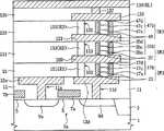
参考图3,在半导体基板1的预定区域中提供隔离层3以限定有源区3a。主源极区9s和主漏极区9d被设置在有源区3a中,并且主栅极电极7a被设置在主源极9s和主漏极9d之间的沟道区上。主栅极电极7a通过栅极绝缘层5与沟道区绝缘。主栅极电极7a可延伸以与有源区3a交叉(即基本上垂直于有源区3a),并且可用作主字线(与图1的WL0对应)。另一个主栅极电极7b可被设置在与主源极9s相邻的有源区3a上。也就是说,主源极9s可被设置在主栅极电极7a和7b之间的有源区中。主栅极电极7a、主源极9s和主漏极9d限定了主开关设备(与图1的SW0对应)。Referring to FIG. 3, an
下部绝缘层11形成在主开关设备9s、9d和7a以及绝缘层3上。公共源极线13s和漏极焊盘13d可提供在下部绝缘层11中。公共源极线13s可被设置成与主字线7a平行。公共源极线13s和漏极焊盘13d可分别通过穿过下部绝缘层11的源极接触孔11s和漏极接触孔11d电连接到主源极9s和主漏极9d。The lower insulating
第一绝缘层15被设置在公共源极线13s、漏极焊盘13d和下部绝缘层11上,且第一开关设备SW1被设置在第一绝缘层15中。第一开关设备SW1包括穿过第一绝缘层15延伸的第一主体图案17b和包围第一主体图案17b的第一栅极电极23。第一主体图案17b包括顺序地垂直叠置的第一源极17s、第一沟道17c和第一漏极17d。第一栅极电极23位于第一沟道17c的侧壁上,并且第一沟道17c电连接到漏极焊盘13d。因此,第一开关设备SW1可以是垂直型MOS晶体管。第一栅极电极23与主字线7a平行地延伸并用作第一字线(图1的WL1)。The first insulating
第一下电极27(与图1的第一加热器H1对应)被设置在与第一开关设备SW1相邻的第一绝缘层15中。第一下电极27电连接到漏极焊盘13d。第一相变材料图案29(与图1的第一可变电阻器R1对应)形成在第一下电极27的上表面和第一漏极17d的上表面上,并且第一上电极31叠置在第一相变材料图案29上。第一下电极27、第一相变材料图案29和第一上电极31限定了第一数据存储元件。第一相变材料图案29一般显示出初始晶态,但是被配置成响应于施加至其的热量转变成非晶态。第一开关设备SW1和第一数据存储元件27、29和31限定第一电阻存储器单元(与图1的CL1对应),即第一相变存储器单元。A first lower electrode 27 (corresponding to the first heater H1 of FIG. 1 ) is disposed in the first insulating
第二绝缘层33被提供在第一上电极31和第一绝缘层15上。与第一开关设备SW1具有相同配置的第二开关设备SW2被设置在第二绝缘层33中。也就是说,第二开关设备SW2包括穿过第二绝缘层33延伸以与第一上电极31接触的第二主体图案35b和位于第二主体图案35b侧壁上的第二栅极电极37。第二主体图案35b包括顺序叠置的第二源极35s、第二沟道35c和第二漏极35d。第二栅极电极37与第一栅极电极23平行地延伸并用作第二字线(与图1的WL2对应)。The second insulating
第二数据存储元件被设置成与第二开关设备SW2相邻。第二数据存储元件具有与第一数据存储元件相同的配置。也就是说,第二数据存储元件可包括穿过第二绝缘层33延伸以与第一上电极31电连接的第二下电极39(与图1的第二加热器H2对应),和位于第二下电极39和第二漏极35d上的第二相变材料图案41(与图1的第二可变电阻器R2对应),以及位于第二相变材料图案41上的第二上电极43。第二相变材料图案41也具有初始晶态。第二开关设备SW2和第二数据存储元件39、41和43限定了第二电阻存储器单元(与图1的CL2对应),即第二相变存储器单元。The second data storage element is arranged adjacent to the second switching device SW2. The second data storage element has the same configuration as the first data storage element. That is, the second data storage element may include a second
第三绝缘层45被提供在第二上电极43和第二绝缘层33上。与第一开关设备SW1具有相同配置的第三开关设备SW3被设置在第三绝缘层45中。也就是说,第三开关设备SW3包括穿过第三绝缘层45延伸以与第二上电极43接触的第三主体图案47b和位于第三主体图案47b侧壁上的第三栅极电极49。第三主体图案47b包括顺序叠置的第三源极47s、第三沟道47c和第三漏极47d。第三栅极电极49可与第一字线23平行地延伸并可用作第三字线(与图1的WL3对应)。The third insulating
第三数据存储元件被设置成与第三开关设备SW3相邻。第三数据存储元件可具有与第一数据存储元件相同的配置。也就是说,第三数据存储元件可包括穿过第三绝缘层45延伸以与第二上电极43电连接的第三下电极51(与图1的第三加热器H3对应)、位于第三下电极51和第三漏极47d上的第三相变材料图案53,以及在第三相变材料图案53上的第三上电极55。第三相变材料图案53也具有初始晶态。第三开关设备SW3和第三数据存储元件51、53和55限定了第三电阻存储器单元(与图1的CL3对应),即第三相变存储器单元。The third data storage element is disposed adjacent to the third switching device SW3. The third data storage element may have the same configuration as the first data storage element. That is, the third data storage element may include a third lower electrode 51 (corresponding to the third heater H3 of FIG. The third phase
上部绝缘层57被设置在第三上电极55和第三绝缘层45上,并且位线61(与图1的BL对应)被设置在上部绝缘层57上。位线61可经由穿过上部绝缘层57延伸的位线接触插塞59电连接到第三上电极55。位线61可被设置成与主字线7a交叉。An upper insulating
因此,根据图3实施例的NAND型电阻存储器单元串包括形成在半导体基板1上的主开关设备,顺序叠置在主开关设备上以使多个电阻存储器单元中的第一个的上电极位于多个电阻存储器单元中的下一个的下电极和主体图案上的多个电阻存储器单元,以及电连接到多个电阻存储器单元中最后一个的位线。主开关设备电连接到多个电阻存储器单元中的第一个,并且多个叠置电阻存储器单元相互串联连接。Therefore, the NAND type resistance memory cell string according to the embodiment of FIG. The lower electrode of the next one of the plurality of resistance memory cells and the plurality of resistance memory cells on the body pattern, and the bit line electrically connected to the last one of the plurality of resistance memory cells. The main switching device is electrically connected to a first one of the plurality of resistive memory cells, and the plurality of stacked resistive memory cells are connected to each other in series.
可使用与以上参考图1所描述的相同方法来选择性编程和读取图3中所示的第一到第三电阻存储器单元中的一个。因此,将不进一步描述根据图3实施例的NAND型电阻存储器单元串的操作。One of the first to third resistance memory cells shown in FIG. 3 may be selectively programmed and read using the same method as described above with reference to FIG. 1 . Therefore, the operation of the NAND-type resistive memory cell string according to the embodiment of FIG. 3 will not be further described.
当选择性编程第一电阻存储器单元时,在第一相变材料图案29和第一下电极27之间的界面处产生焦耳热,以使得第一相变材料图案29(即与第一下电极27的上表面相邻的第一相变区29v)至少部分被转变成结晶态或非晶态。因此,第一相变材料图案29可根据图案29处于结晶态还是非晶态在第一电阻和高于第一电阻的第二电阻之间转换。类似地,当选择性编程第二电阻存储器单元时,第二相变材料图案41(即与第二下电极39的上表面相邻的第二相变区41v)可至少部分被转变成结晶态或非晶态,并且当选择性编程第三电阻存储器单元时,第三相变材料图案53(即与第三下电极51的上表面相邻的第三相变区53v)可至少部分被转变成结晶态或非晶态。When the first resistive memory cell is selectively programmed, Joule heat is generated at the interface between the first phase-
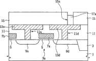
图4是具有图1中所示的等效电路图的另一NAND型电阻存储器单元串的截面图。图4的实施例在数据存储元件类型方面不同于图3的实施例。FIG. 4 is a cross-sectional view of another NAND-type resistive memory cell string having the equivalent circuit diagram shown in FIG. 1 . The embodiment of FIG. 4 differs from the embodiment of FIG. 3 in the type of data storage element.
参考图4,与图3中所示配置相同的主开关设备7a、9s和9d、下部绝缘层11、漏极焊盘13d和公共源极线13s被提供在半导体基板1上。第一绝缘层15被设置在下部绝缘层11、漏极焊盘13d和公共源极线13s上,并且具有与图3中所示的相同配置的第一开关设备SW1被设置在第一绝缘层15中。借助于穿过第一绝缘层15的第一孔101,漏极焊盘13d被暴露出来,并且第一下电极103(与图1的第一加热器H1对应)被设置在第一孔101中。第一下电极103可被凹陷以具有低于第一绝缘层15的上表面的上表面。第一下电极103的第一孔101可被第一相变材料图案107填充(与图1的第一可变电阻器R1对应)。此外,第一绝缘隔离物105可插入在第一相变材料图案107的侧壁与第一绝缘层15之间。也就是说,在图4的实施例中,第一相变材料图案107可与第一下电极103自对准。换句话说,第一相变材料图案107可具有由第一孔101侧壁上的隔离物105限定的形状。第一上电极109被形成在第一相变材料图案107和第一漏极17d上。第一下电极103、第一相变材料图案107和第一上电极109限定了第一数据存储元件。第一开关设备SW1和第一数据存储元件103、107和109限定了第一电阻存储器单元(与图1的CL1对应),即第一相变存储器单元。Referring to FIG. 4 ,
如图4中所示,第一上电极109与第一漏极17d的上表面接触。因此,与图3的实施例相比,第一上电极109与第一开关设备SW1之间的寄生电阻可被显著降低。特别是,虽然在图3的示范性实施例中第一相变材料图案29在第一上电极31与第一开关设备SW1之间延伸,但是在图4的实施例中没有这种电阻材料层在第一上电极109与第一开关设备SW1之间延伸。As shown in FIG. 4, the first
第二绝缘层111被设置在第一绝缘层15和第一上电极109上。具有与图3中所示相同配置的第二开关设备SW2被设置在第二绝缘层111中。而且,与第一数据存储元件103、107和109具有相同配置的第二数据存储元件被设置在第二绝缘层111中。也就是说,第二数据存储元件可包括穿过第二绝缘层111且电连接到第一上电极109的第二下电极115(与图1的第二加热器H2对应)、位于第二下电极115上的第二相变材料图案119(与图1的第二可变材料RS对应),以及位于第二相变材料图案119和第二漏极35d上的第二上电极121。第二绝缘隔离物117可插入在第二相变材料图案119的侧壁与第二绝缘层111之间。如图4中所示,第二上电极121可与第二上部漏极35d的上表面接触。第二开关设备SW2和第二数据存储元件115、119和121限定第二电阻存储器单元(与图1的CL2对应),即第二相变存储器单元。The second
第三绝缘层123被设置在第二绝缘层111和第二上电极121上,并且具有与图3中所示相同配置的第三开关设备SW3被设置在第三绝缘层123中。而且,具有与第一数据存储元件103、107和109相同配置的第三数据存储元件被设置在第三绝缘层123中。也就是说,第三数据存储元件可包括穿过第三绝缘层123且与第二上电极121电连接的第三下电极127(与图1的第三加热器H3对应)、位于第三下电极127上的第三相变材料图案131(与图1的第三可变电阻器R3对应),以及位于第三相变材料图案131和第三漏极47d上的第三上电极133。第三绝缘隔离物129可插入在第三相变材料图案131的侧壁与第三绝缘层123之间。如图4中所示,第三上电极133可与第三漏极47d的上表面直接接触。第三开关设备SW3和第三数据存储元件127、131和133限定第三电阻存储器单元(与图1的CL3对应),即第三相变存储器单元。A third insulating
上部绝缘层135被设置在第三上电极133和第三绝缘层123上,且位线139(与图1的BL对应)被设置在上部绝缘层135上。位线139可经由穿过上部绝缘层135的位线接触插塞137电连接到第三上电极133。位线139可被设置成与主字线7a交叉。An upper insulating
可使用与参考图1所描述的相同方法来选择性地编程和读取图4中所示的第一至第三电阻存储器单元。因此,以下不再进一步描述根据图4实施例的NAND型电阻存储器单元串的进一步操作。The first to third resistance memory cells shown in FIG. 4 may be selectively programmed and read using the same method as described with reference to FIG. 1 . Therefore, the further operation of the NAND-type resistive memory cell string according to the embodiment of FIG. 4 will not be further described below.
根据图4的实施例,第一至第三上电极109、121和133可分别与第一至第三漏极17d、35d和47d直接接触,如上所述。因此,与图3的示范性实施例相比,可显著降低上电极109、121和133与开关设备SW1、SW2和SW3之间的寄生电阻。当降低寄生电阻时,流过未被选择的电阻存储器单元开关设备的电流会增加,且这导致了抑制未被选择的电阻存储器单元的数据存储元件的软编程。此外,当降低寄生电阻时,会增加读出放大器的读出裕量。According to the embodiment of FIG. 4, the first to third
图5是具有图2等效电路图的又一个NAND型电阻存储器单元串的截面图。图5的实施例在数据存储元件类型方面不同于图4的实施例。也就是说,根据图5的实施例,提供第一可变电阻器151代替图4的第一下电极103、第一相变材料图案107和第一绝缘隔离物105,并且提供第二可变电阻器153代替图4的第二下电极115、第二相变材料图案119和第二绝缘隔离物117。类似地,提供第三可变电阻器155代替图4的第三下电极127、第三相变材料图案131和第三绝缘隔离物129。因此,第一、第二和第三可变电阻器151、153和155可分别与第一至第三开关设备SW1至SW3并联连接。FIG. 5 is a cross-sectional view of yet another NAND-type resistive memory cell string having the equivalent circuit diagram of FIG. 2 . The embodiment of FIG. 5 differs from the embodiment of FIG. 4 in the type of data storage element. That is, according to the embodiment of FIG. 5, the first
第一、第二和第三可变电阻器151、153和155中的每一个都包括用于RRAM单元(例如PCMO层或过渡金属氧化物层)的可变电阻器。相反,第一、第二和第三可变电阻器151、153和155可以是用于MRAM单元的相应的电磁隧穿结(MTJ)结构。也就是说,第一、第二和第三可变电阻器151、153和155每一个都可包括顺序叠置的钉扎层、隧穿绝缘层和自由层。Each of the first, second and third
以下将描述根据本发明的另外实施例的制造NAND型电阻存储器单元串的方法。A method of manufacturing a NAND-type resistive memory cell string according to another embodiment of the present invention will be described below.
图6A至13A是示出制造图3中所示的NAND型电阻存储器单元串的方法的平面图,并且图6B至13B是分别与图6A至13A对应的截面图。6A to 13A are plan views illustrating a method of manufacturing the NAND type resistance memory cell string shown in FIG. 3, and FIGS. 6B to 13B are cross-sectional views corresponding to FIGS. 6A to 13A, respectively.
参考图6A和6B,隔离层3形成在基板1的预定区域中以限定有源区3a。栅极绝缘层5形成在有源区上,并且栅极传导层形成在具有栅极绝缘层5的基板上。栅极传导层被图案化以形成与有源区3a交叉的主栅极电极7a和7b。可使用主栅极电极7a和7b和隔离层3作为离子注入掩模将杂质离子注入到有源区3a中,从而形成主源极区9s和主漏极区9d。主栅极电极7a、主源极9s和主漏极9d限定了主开关设备(图1的SW0)。Referring to FIGS. 6A and 6B, an
下部绝缘层11被形成在具有主开关设备7a、9s和9d的基板上。使用公知的方法将公共源极线13s和漏极焊盘13d形成在下部绝缘层11中/上。公共源极线13s被形成为通过穿过下部绝缘层11的源极接触孔11s与主源极9s接触,并且漏极焊盘13d被形成为通过穿过下部绝缘层11的漏极接触孔11d与主漏极9d接触。主栅极电极7a和公共源极线13s可与有源区3a交叉形成,如图6A中所示。The lower insulating
参考图7A和7B,第一绝缘层15被形成在具有公共源极线13s和漏极焊盘13d的基板上,并且第一绝缘层15被图案化以形成暴露漏极焊盘13d的第一区域的第一主体孔15a。之后,诸如硅层的半导体层被形成在第一主体孔15a中和第一绝缘层15上,并且半导体层被平坦化以暴露第一绝缘层15的上表面。结果,半导体图案可形成在第一主体孔15a中。半导体图案被图案化以在第一主体孔15a中形成凹陷的半导体图案17a。如图7B中所示,凹陷的半导体图案17a可具有低于第一绝缘层15的上表面的上表面。Referring to FIGS. 7A and 7B, a first insulating
参考图8A和8B,将杂质离子注入到凹陷的半导体图案17a中以形成顺序叠置的第一源极17s、第一沟道17c和第一漏极17d。第一源极17s、第一沟道17c和第一漏极17d限定了第一主体图案17d。之后,第一主体覆盖(capping)图案19被形成在第一主体图案17b上的第一主体孔15a中。第一主体覆盖图案19可由相对第一绝缘层15具有蚀刻选择性的材料层形成。例如,当第一绝缘层15由二氧化硅层形成时,第一主体覆盖图案19由诸如氮化硅层或氮氧化硅层之类的绝缘层形成。8A and 8B, impurity ions are implanted into the recessed
参考图9A和9B,第一绝缘层15被图案化以形成暴露出第一主体图案17b和第一主体覆盖图案19的侧壁的第一沟槽15b。如图9A中所示,可形成平行于公共源极线13s延伸的第一沟槽15b。而且,第一沟槽15b可被形成为至少暴露出第一沟道17c的侧壁。也就是说,在一些实施例中,第一沟槽15b可被形成为使得与第一源极17s相邻的漏极焊盘13d不被暴露。相反,在其他实施例中,第一沟槽15b可被形成为暴露出与第一源极17s相邻的漏极焊盘13d。这种情况下,第一沟槽15b可暴露出第一源极17s的侧壁、第一沟道17c、第一漏极17d和第一主体覆盖图案19。Referring to FIGS. 9A and 9B , the first insulating
第一栅极绝缘层21被形成在基板上和第一沟槽15b中。第一栅极绝缘层21可使用公知的沉积技术,例如化学气相沉积(CVD)技术、原子层沉积(ALD)技术和/或热氧化技术形成。第一栅极绝缘层21可选择性地形成在漏极焊盘13d的暴露区域和/或第一主体图案17b的侧壁上。A first
栅极传导层被形成在第一栅极绝缘层21上,并且栅极传导层被平坦化以在第一沟槽15b中形成第一栅极电极23。第一栅极电极23可被凹陷以具有低于第一绝缘层15的上表面的上表面。更具体地,第一栅极电极23可被凹陷以具有比第一漏极17d的上表面低的上表面。第一栅极电极23和第一主体图案17b限定了第一开关设备SW1,即第一垂直MOS晶体管。A gate conductive layer is formed on the first
参考图10A和10B,第一栅极覆盖绝缘层被形成在形成了第一栅极电极23的基板上,并且第一栅极覆盖绝缘层被平坦化以形成保留在第一栅极电极23上的第一沟槽15b中的第一栅极覆盖图案25。Referring to FIGS. 10A and 10B, a first gate covering insulating layer is formed on the substrate on which the
参考图11A和11B,第一主体覆盖图案19被去除以暴露出第一漏极17d,并且第一绝缘层15被图案化以形成暴露出漏极焊盘13d的第二区域且与第一主体图案17b横向隔开的第一孔15c。在一些实施例中,在形成第一孔15c之后,可去除第一主体覆盖图案19。11A and 11B, the first
参考图12A和12B,第一下电极27形成在第一孔15c中。可通过在具有第一孔15c的基板上沉积诸如氮化钛(TiN)层和/或氮化钛铝(TiAlN)层之类的下电极层以及平坦化下电极层来形成第一下电极27。12A and 12B, the first
可变电阻器材料层和上电极材料层顺序形成在具有第一下电极27的基板上,并且上电极材料层和可变电阻器材料层被图案化以形成在第一下电极27和第一漏极17d上的第一可变电阻器29和叠置在第一可变电阻器29上的第一上电极31。可变电阻器层可由诸如硫族化物层的相变材料层形成,并且上电极层可由诸如氮化钛(TiN)层和/或氮化钛铝(TiAlN)层之类的传导层形成。第一下电极27、第一可变电阻器29和第一上电极31限定了第一数据存储元件。而且,第一数据存储元件27、29和31以及第一开关设备SW1限定了第一电阻存储器单元,即第一相变存储器单元(与图1的CL1对应)。The variable resistor material layer and the upper electrode material layer are sequentially formed on the substrate having the first
参考图13A和13B,第二绝缘层33被形成在第一上电极31和第一绝缘层15上,并且使用与参考图7A至12B所描述的相似方法将第二开关设备SW2和第二下电极39形成在第一绝缘层33中。使用与参考图12A和12B所描述的方法类似的方法,形成位于第二下电极39和第二开关设备SW2上的第二可变电阻器41以及叠置在第二可变电阻器41上的第二上电极43。第二下电极39、第二可变电阻器41以及第二上电极43限定了第二数据存储元件,并且第二数据存储元件和第二开关设备SW2限定了第二电阻存储器单元,即第二相变存储器单元(图1的CL2)。Referring to FIGS. 13A and 13B, a second insulating
第三绝缘层45被形成在第二电阻存储器单元上,并且使用与参考图7A至12B所描述的相似方法将第三开关设备SW3和第三下电极51形成在第三绝缘层45中。可使用与参考图12A和12B所描述的方法类似的方法形成在第三下电极51和第三开关设备SW3上的第三可变电阻器53以及叠置在第三可变电阻器53上的第三上电极55。第三下电极51、第三可变电阻器53以及第三上电极55限定第三数据存储元件,并且第三数据存储元件51、53和55和第三开关设备SW3限定了第三电阻存储器单元,即第三相变存储器单元(图1的CL3)。The third insulating
上部绝缘层57被形成在具有第三电阻存储器单元的基板上,并且电连接到第三上电极55的位线接触插塞59被形成在上部绝缘层57中。诸如金属层的传导层被形成在具有位线接触插塞59的基板上,并且传导层被图案化以形成在位线接触插塞59上的位线61。位线61可被形成为在平面图上与主栅极电极7a交叉。An upper insulating
图14至17是示出制造图4中所示的NAND型电阻存储器单元串的方法的截面图。14 to 17 are cross-sectional views showing a method of manufacturing the NAND type resistance memory cell string shown in FIG. 4 .
参考图14和15,通过使用与参考图6A至10B所描述的方法类似的方法,将主开关设备7a、9s和9d、下部绝缘层11、公共源极线13s、漏极焊盘13d、第一绝缘层15以及第一开关设备SW1形成在半导体基板1上。第一绝缘层15被图案化以形成暴露出漏极焊盘13d的预定区域的第一孔101,并且在第一孔101中形成第一下电极103。在形成第一孔101之前或之后,可去除在第一开关设备SW1的第一主体图案17b上的第一主体覆盖图案19。第一下电极103可由诸如TiN层或TiAlN层之类的传导层形成。而且,第一下电极103可被凹陷以使得其具有低于第一绝缘层15的上表面的上表面。14 and 15, by using a method similar to that described with reference to FIGS. An insulating
参考图16,第一绝缘隔离物105可形成在第一下电极103上的第一孔101的侧壁上。第一绝缘隔离物105可由相对第一绝缘层15具有蚀刻选择性的材料层形成。例如,当第一绝缘层15由氧化硅层形成时,第一绝缘隔离物105可由氮化硅层和/或氮氧化硅层形成。可变电阻器层可形成在基板上和其中具有第一绝缘隔离物105的第一孔101中,并且可变电阻器层被平坦化以形成在由第一绝缘隔离物105包围的第一孔101中的第一可变电阻器107。可变电阻层可由诸如硫族化物层的相变材料层形成。因此,第一可变电阻器107可通过第一孔101与第一下电极103自对准,且可被形成为具有受限形状。Referring to FIG. 16 , a first insulating
上电极层被形成在具有第一可变电阻器107的基板上,并且上电极层被图案化以形成在第一可变电阻器107和第一漏极17d上的第一上电极109。上电极层可由诸如TiN层或TiAlN层之类的传导层形成。An upper electrode layer is formed on the substrate having the first
第一下电极103、第一可变电阻器107和第一上电极109限定了第一数据存储元件,并且第一数据存储元件103、107和109以及第一开关设备SW1限定了第一电阻存储器单元,即第一相变存储器单元(与图1的CL1对应)。The first
参考图17,第二绝缘层111被形成在具有第一上电极109的基板上,并且使用与参考图14所描述的相似方法将第二开关设备SW2形成在第二绝缘层111中。第二绝缘层111被图案化以形成暴露出第二下电极115和第一上电极109的预定区域的第二孔113,并且使用与参考图15和16所描述的方法类似的方法将第二绝缘隔离物117以及第二可变电阻器119形成在第二孔113中。第二上电极121可被形成在第二可变电阻器119和第二漏极35d上。Referring to FIG. 17 , a second insulating
第二下电极115、第二可变电阻器119和第二上电极121限定了第二数据存储元件,并且第二数据元件115、119和121以及第二开关设备SW2限定了第二电阻存储器单元,即第二相变存储器单元(图1的CL2)。The second
第三绝缘层123被形成在第二上电极121和第二绝缘层111上,并且使用与参考图14所描述的相似方法将第三开关设备SW3形成在第三绝缘层123中。第三绝缘层123被图案化以形成暴露出第三下电极127、第二上电极121的预定区域的第三孔125,并且使用与参考图15和16所述的相似方法将第三绝缘隔离物129和第三可变电阻器131形成在第三孔125中。第三上电极133被形成在第三可变电阻器131和第三漏极47d中。The third
第三下电极127、第三可变电阻器131和第三上电极133限定了第三数据存储元件,并且第三数据存储元件127、131和133以及第三开关设备SW3限定了第三电阻存储器单元,即第三相变存储器单元(与图1的CL3对应)。The third
上部绝缘层135被形成在第三上电极133和第三绝缘层123上,并且位线139被形成在上部绝缘层135上。位线139经由穿过上部绝缘层135延伸的位线接触插塞137电连接到第三上电极133。位线139可使用与参考图13A和13B所描述的相似方法形成。An upper insulating
制造图5中所示的NAND型电阻存储器单元串的方法不同于参考图14至17所描述的实施例中的方法,特别在于制造第一至第三可变电阻器151、153和155方面。也就是说,第一至第三可变电阻器151、153和155中的每一个都由用于RRAM单元(例如镨钙锰氧化物(PCMO)层和/或过渡金属氧化物层)的可变电阻器形成。替换地,第一、第二和第三可变电阻器151、153和155中的每一个都可使用用于一般MRAM单元的制造磁性隧穿结(MTJ)结构的方法来制造。也就是说,第一、第二和第三可变电阻器151、153和155中的每一个都可形成为包括顺序叠置的钉扎层、隧穿绝缘层和自由层。The method of manufacturing the NAND type resistance memory cell string shown in FIG. 5 is different from the method in the embodiment described with reference to FIGS. That is, each of the first to third
根据上述实施例,在半导体基板上垂直叠置多个串联连接的电阻存储器单元,并且每一个电阻存储器单元都被形成为包括包含可变电阻器的数据存储元件和并联连接到数据存储元件的开关设备。因此,能够提高非易失性存储器件的NAND型电阻存储器单元串的集成密度。According to the above-described embodiments, a plurality of series-connected resistance memory cells are vertically stacked on a semiconductor substrate, and each resistance memory cell is formed to include a data storage element including a variable resistor and a switch connected in parallel to the data storage element equipment. Therefore, the integration density of the NAND-type resistance memory cell strings of the nonvolatile memory device can be increased.
在此已经公开了本发明的实施例,并且,尽管采用了特定术语,但是使用其并仅将其解释为一般的和说明性的含义,且不作为限制目的。因此,本领域技术人员将理解,在不脱离所附的权利要求中所列的本发明的精神和范围的情况下,可作出形式和细节上的各种改变。Embodiments of the present invention have been disclosed herein, and, while specific terms are employed, they are used and are to be construed in a generic and descriptive sense only and not for purposes of limitation. Accordingly, it will be understood by those skilled in the art that various changes in form and details may be made without departing from the spirit and scope of the present invention as set forth in the appended claims.
Claims (12)
Translated fromChineseApplications Claiming Priority (3)
| Application Number | Priority Date | Filing Date | Title |
|---|---|---|---|
| KR10-2007-0075044 | 2007-07-26 | ||
| KR1020070075044 | 2007-07-26 | ||
| KR1020070075044AKR101258268B1 (en) | 2007-07-26 | 2007-07-26 | NAND-type resistive memory cell strings of a non-volatile memory device and methods of fabricating the same |
Publications (2)
| Publication Number | Publication Date |
|---|---|
| CN101354917A CN101354917A (en) | 2009-01-28 |
| CN101354917Btrue CN101354917B (en) | 2014-05-07 |
Family
ID=40157620
Family Applications (1)
| Application Number | Title | Priority Date | Filing Date |
|---|---|---|---|
| CN200810131101.7AActiveCN101354917B (en) | 2007-07-26 | 2008-07-28 | Non-volatile memory devices including stacked nand-type resistive memory cell strings and methods of fabricating the same |
Country Status (6)
| Country | Link |
|---|---|
| US (2) | US7843718B2 (en) |
| JP (1) | JP5661992B2 (en) |
| KR (1) | KR101258268B1 (en) |
| CN (1) | CN101354917B (en) |
| DE (1) | DE102008034003B4 (en) |
| TW (1) | TWI517359B (en) |
Families Citing this family (275)
| Publication number | Priority date | Publication date | Assignee | Title |
|---|---|---|---|---|
| KR100795350B1 (en)* | 2006-11-24 | 2008-01-17 | 삼성전자주식회사 | Nonvolatile memory device, manufacturing method and operating method thereof. |
| US7825486B2 (en)* | 2008-01-16 | 2010-11-02 | International Business Machines Corporation | Memory cell and memory device |
| JP4596070B2 (en) | 2008-02-01 | 2010-12-08 | ソニー株式会社 | Memory device, method for manufacturing memory device, display device, and method for manufacturing display device |
| KR100960462B1 (en)* | 2008-04-18 | 2010-05-31 | 주식회사 하이닉스반도체 | Phase change memory device and forming method thereof |
| KR100960461B1 (en)* | 2008-04-18 | 2010-05-28 | 주식회사 하이닉스반도체 | Phase change memory device and forming method thereof |
| KR101486984B1 (en)* | 2008-10-30 | 2015-01-30 | 삼성전자주식회사 | Variable resistance memory device and method of forming the same |
| US8130556B2 (en)* | 2008-10-30 | 2012-03-06 | Sandisk Technologies Inc. | Pair bit line programming to improve boost voltage clamping |
| US7916528B2 (en)* | 2009-03-30 | 2011-03-29 | Seagate Technology Llc | Predictive thermal preconditioning and timing control for non-volatile memory cells |
| US9577642B2 (en) | 2009-04-14 | 2017-02-21 | Monolithic 3D Inc. | Method to form a 3D semiconductor device |
| US9509313B2 (en) | 2009-04-14 | 2016-11-29 | Monolithic 3D Inc. | 3D semiconductor device |
| US8058137B1 (en) | 2009-04-14 | 2011-11-15 | Monolithic 3D Inc. | Method for fabrication of a semiconductor device and structure |
| US8395191B2 (en) | 2009-10-12 | 2013-03-12 | Monolithic 3D Inc. | Semiconductor device and structure |
| US8669778B1 (en) | 2009-04-14 | 2014-03-11 | Monolithic 3D Inc. | Method for design and manufacturing of a 3D semiconductor device |
| US8362482B2 (en) | 2009-04-14 | 2013-01-29 | Monolithic 3D Inc. | Semiconductor device and structure |
| US8754533B2 (en) | 2009-04-14 | 2014-06-17 | Monolithic 3D Inc. | Monolithic three-dimensional semiconductor device and structure |
| KR101548675B1 (en) | 2009-08-11 | 2015-09-01 | 삼성전자주식회사 | Variable resistance memory and memory system including it |
| US9099424B1 (en) | 2012-08-10 | 2015-08-04 | Monolithic 3D Inc. | Semiconductor system, device and structure with heat removal |
| US10354995B2 (en) | 2009-10-12 | 2019-07-16 | Monolithic 3D Inc. | Semiconductor memory device and structure |
| US10157909B2 (en) | 2009-10-12 | 2018-12-18 | Monolithic 3D Inc. | 3D semiconductor device and structure |
| US8148728B2 (en) | 2009-10-12 | 2012-04-03 | Monolithic 3D, Inc. | Method for fabrication of a semiconductor device and structure |
| US10366970B2 (en) | 2009-10-12 | 2019-07-30 | Monolithic 3D Inc. | 3D semiconductor device and structure |
| US11018133B2 (en) | 2009-10-12 | 2021-05-25 | Monolithic 3D Inc. | 3D integrated circuit |
| US8476145B2 (en) | 2010-10-13 | 2013-07-02 | Monolithic 3D Inc. | Method of fabricating a semiconductor device and structure |
| US11374118B2 (en) | 2009-10-12 | 2022-06-28 | Monolithic 3D Inc. | Method to form a 3D integrated circuit |
| US10043781B2 (en) | 2009-10-12 | 2018-08-07 | Monolithic 3D Inc. | 3D semiconductor device and structure |
| US12027518B1 (en) | 2009-10-12 | 2024-07-02 | Monolithic 3D Inc. | 3D semiconductor devices and structures with metal layers |
| US11984445B2 (en) | 2009-10-12 | 2024-05-14 | Monolithic 3D Inc. | 3D semiconductor devices and structures with metal layers |
| US10910364B2 (en) | 2009-10-12 | 2021-02-02 | Monolitaic 3D Inc. | 3D semiconductor device |
| US10388863B2 (en) | 2009-10-12 | 2019-08-20 | Monolithic 3D Inc. | 3D memory device and structure |
| US8742476B1 (en) | 2012-11-27 | 2014-06-03 | Monolithic 3D Inc. | Semiconductor device and structure |
| US8541819B1 (en) | 2010-12-09 | 2013-09-24 | Monolithic 3D Inc. | Semiconductor device and structure |
| US8026521B1 (en) | 2010-10-11 | 2011-09-27 | Monolithic 3D Inc. | Semiconductor device and structure |
| US9099526B2 (en) | 2010-02-16 | 2015-08-04 | Monolithic 3D Inc. | Integrated circuit device and structure |
| US8492886B2 (en) | 2010-02-16 | 2013-07-23 | Monolithic 3D Inc | 3D integrated circuit with logic |
| US8461035B1 (en) | 2010-09-30 | 2013-06-11 | Monolithic 3D Inc. | Method for fabrication of a semiconductor device and structure |
| US8198160B2 (en)* | 2010-04-19 | 2012-06-12 | Jun Liu | Vertical transistor phase change memory |
| US8367460B2 (en)* | 2010-06-22 | 2013-02-05 | Micron Technology, Inc. | Horizontally oriented and vertically stacked memory cells |
| US8901613B2 (en) | 2011-03-06 | 2014-12-02 | Monolithic 3D Inc. | Semiconductor device and structure for heat removal |
| US9953925B2 (en) | 2011-06-28 | 2018-04-24 | Monolithic 3D Inc. | Semiconductor system and device |
| US10217667B2 (en) | 2011-06-28 | 2019-02-26 | Monolithic 3D Inc. | 3D semiconductor device, fabrication method and system |
| US9219005B2 (en) | 2011-06-28 | 2015-12-22 | Monolithic 3D Inc. | Semiconductor system and device |
| US8642416B2 (en) | 2010-07-30 | 2014-02-04 | Monolithic 3D Inc. | Method of forming three dimensional integrated circuit devices using layer transfer technique |
| CN102959635B (en)* | 2010-09-08 | 2015-06-03 | 株式会社日立制作所 | Semiconductor memory device |
| CN101958148B (en)* | 2010-09-21 | 2012-10-10 | 中国科学院上海微系统与信息技术研究所 | Phase change random access memory unit structure capable of eliminating interference and phase change random access memory formed by same |
| US10497713B2 (en) | 2010-11-18 | 2019-12-03 | Monolithic 3D Inc. | 3D semiconductor memory device and structure |
| US8163581B1 (en) | 2010-10-13 | 2012-04-24 | Monolith IC 3D | Semiconductor and optoelectronic devices |
| US11482440B2 (en) | 2010-12-16 | 2022-10-25 | Monolithic 3D Inc. | 3D semiconductor device and structure with a built-in test circuit for repairing faulty circuits |
| US8273610B2 (en) | 2010-11-18 | 2012-09-25 | Monolithic 3D Inc. | Method of constructing a semiconductor device and structure |
| US12362219B2 (en) | 2010-11-18 | 2025-07-15 | Monolithic 3D Inc. | 3D semiconductor memory device and structure |
| US11024673B1 (en) | 2010-10-11 | 2021-06-01 | Monolithic 3D Inc. | 3D semiconductor device and structure |
| US10896931B1 (en) | 2010-10-11 | 2021-01-19 | Monolithic 3D Inc. | 3D semiconductor device and structure |
| US11469271B2 (en) | 2010-10-11 | 2022-10-11 | Monolithic 3D Inc. | Method to produce 3D semiconductor devices and structures with memory |
| US11018191B1 (en) | 2010-10-11 | 2021-05-25 | Monolithic 3D Inc. | 3D semiconductor device and structure |
| US11227897B2 (en) | 2010-10-11 | 2022-01-18 | Monolithic 3D Inc. | Method for producing a 3D semiconductor memory device and structure |
| US11600667B1 (en) | 2010-10-11 | 2023-03-07 | Monolithic 3D Inc. | Method to produce 3D semiconductor devices and structures with memory |
| US11257867B1 (en) | 2010-10-11 | 2022-02-22 | Monolithic 3D Inc. | 3D semiconductor device and structure with oxide bonds |
| US11158674B2 (en) | 2010-10-11 | 2021-10-26 | Monolithic 3D Inc. | Method to produce a 3D semiconductor device and structure |
| US11315980B1 (en) | 2010-10-11 | 2022-04-26 | Monolithic 3D Inc. | 3D semiconductor device and structure with transistors |
| US10290682B2 (en) | 2010-10-11 | 2019-05-14 | Monolithic 3D Inc. | 3D IC semiconductor device and structure with stacked memory |
| JP5588816B2 (en)* | 2010-10-12 | 2014-09-10 | 株式会社日立製作所 | Semiconductor memory device |
| JP5427959B2 (en)* | 2010-10-12 | 2014-02-26 | 株式会社日立製作所 | Semiconductor memory device |
| US12080743B2 (en) | 2010-10-13 | 2024-09-03 | Monolithic 3D Inc. | Multilevel semiconductor device and structure with image sensors and wafer bonding |
| US11605663B2 (en) | 2010-10-13 | 2023-03-14 | Monolithic 3D Inc. | Multilevel semiconductor device and structure with image sensors and wafer bonding |
| US10943934B2 (en) | 2010-10-13 | 2021-03-09 | Monolithic 3D Inc. | Multilevel semiconductor device and structure |
| US10978501B1 (en) | 2010-10-13 | 2021-04-13 | Monolithic 3D Inc. | Multilevel semiconductor device and structure with waveguides |
| US11133344B2 (en) | 2010-10-13 | 2021-09-28 | Monolithic 3D Inc. | Multilevel semiconductor device and structure with image sensors |
| US11063071B1 (en) | 2010-10-13 | 2021-07-13 | Monolithic 3D Inc. | Multilevel semiconductor device and structure with waveguides |
| US10998374B1 (en) | 2010-10-13 | 2021-05-04 | Monolithic 3D Inc. | Multilevel semiconductor device and structure |
| US10833108B2 (en) | 2010-10-13 | 2020-11-10 | Monolithic 3D Inc. | 3D microdisplay device and structure |
| US11437368B2 (en) | 2010-10-13 | 2022-09-06 | Monolithic 3D Inc. | Multilevel semiconductor device and structure with oxide bonding |
| US11855100B2 (en) | 2010-10-13 | 2023-12-26 | Monolithic 3D Inc. | Multilevel semiconductor device and structure with oxide bonding |
| US11929372B2 (en) | 2010-10-13 | 2024-03-12 | Monolithic 3D Inc. | Multilevel semiconductor device and structure with image sensors and wafer bonding |
| US10679977B2 (en) | 2010-10-13 | 2020-06-09 | Monolithic 3D Inc. | 3D microdisplay device and structure |
| US11869915B2 (en) | 2010-10-13 | 2024-01-09 | Monolithic 3D Inc. | Multilevel semiconductor device and structure with image sensors and wafer bonding |
| US9197804B1 (en) | 2011-10-14 | 2015-11-24 | Monolithic 3D Inc. | Semiconductor and optoelectronic devices |
| US12360310B2 (en) | 2010-10-13 | 2025-07-15 | Monolithic 3D Inc. | Multilevel semiconductor device and structure with oxide bonding |
| US11404466B2 (en) | 2010-10-13 | 2022-08-02 | Monolithic 3D Inc. | Multilevel semiconductor device and structure with image sensors |
| US11163112B2 (en) | 2010-10-13 | 2021-11-02 | Monolithic 3D Inc. | Multilevel semiconductor device and structure with electromagnetic modulators |
| US11855114B2 (en) | 2010-10-13 | 2023-12-26 | Monolithic 3D Inc. | Multilevel semiconductor device and structure with image sensors and wafer bonding |
| US11694922B2 (en) | 2010-10-13 | 2023-07-04 | Monolithic 3D Inc. | Multilevel semiconductor device and structure with oxide bonding |
| US11043523B1 (en) | 2010-10-13 | 2021-06-22 | Monolithic 3D Inc. | Multilevel semiconductor device and structure with image sensors |
| US12094892B2 (en) | 2010-10-13 | 2024-09-17 | Monolithic 3D Inc. | 3D micro display device and structure |
| US11164898B2 (en) | 2010-10-13 | 2021-11-02 | Monolithic 3D Inc. | Multilevel semiconductor device and structure |
| US11327227B2 (en) | 2010-10-13 | 2022-05-10 | Monolithic 3D Inc. | Multilevel semiconductor device and structure with electromagnetic modulators |
| US11984438B2 (en) | 2010-10-13 | 2024-05-14 | Monolithic 3D Inc. | Multilevel semiconductor device and structure with oxide bonding |
| US11443971B2 (en) | 2010-11-18 | 2022-09-13 | Monolithic 3D Inc. | 3D semiconductor device and structure with memory |
| US11923230B1 (en) | 2010-11-18 | 2024-03-05 | Monolithic 3D Inc. | 3D semiconductor device and structure with bonding |
| US11004719B1 (en) | 2010-11-18 | 2021-05-11 | Monolithic 3D Inc. | Methods for producing a 3D semiconductor memory device and structure |
| US12068187B2 (en) | 2010-11-18 | 2024-08-20 | Monolithic 3D Inc. | 3D semiconductor device and structure with bonding and DRAM memory cells |
| US11569117B2 (en) | 2010-11-18 | 2023-01-31 | Monolithic 3D Inc. | 3D semiconductor device and structure with single-crystal layers |
| US11107721B2 (en) | 2010-11-18 | 2021-08-31 | Monolithic 3D Inc. | 3D semiconductor device and structure with NAND logic |
| US11482438B2 (en) | 2010-11-18 | 2022-10-25 | Monolithic 3D Inc. | Methods for producing a 3D semiconductor memory device and structure |
| US11784082B2 (en) | 2010-11-18 | 2023-10-10 | Monolithic 3D Inc. | 3D semiconductor device and structure with bonding |
| US11521888B2 (en) | 2010-11-18 | 2022-12-06 | Monolithic 3D Inc. | 3D semiconductor device and structure with high-k metal gate transistors |
| US11482439B2 (en) | 2010-11-18 | 2022-10-25 | Monolithic 3D Inc. | Methods for producing a 3D semiconductor memory device comprising charge trap junction-less transistors |
| US11018042B1 (en) | 2010-11-18 | 2021-05-25 | Monolithic 3D Inc. | 3D semiconductor memory device and structure |
| US11355381B2 (en) | 2010-11-18 | 2022-06-07 | Monolithic 3D Inc. | 3D semiconductor memory device and structure |
| US12272586B2 (en) | 2010-11-18 | 2025-04-08 | Monolithic 3D Inc. | 3D semiconductor memory device and structure with memory and metal layers |
| US11094576B1 (en) | 2010-11-18 | 2021-08-17 | Monolithic 3D Inc. | Methods for producing a 3D semiconductor memory device and structure |
| US11508605B2 (en) | 2010-11-18 | 2022-11-22 | Monolithic 3D Inc. | 3D semiconductor memory device and structure |
| US11355380B2 (en) | 2010-11-18 | 2022-06-07 | Monolithic 3D Inc. | Methods for producing 3D semiconductor memory device and structure utilizing alignment marks |
| US11121021B2 (en) | 2010-11-18 | 2021-09-14 | Monolithic 3D Inc. | 3D semiconductor device and structure |
| US11610802B2 (en) | 2010-11-18 | 2023-03-21 | Monolithic 3D Inc. | Method for producing a 3D semiconductor device and structure with single crystal transistors and metal gate electrodes |
| US11495484B2 (en) | 2010-11-18 | 2022-11-08 | Monolithic 3D Inc. | 3D semiconductor devices and structures with at least two single-crystal layers |
| US12144190B2 (en) | 2010-11-18 | 2024-11-12 | Monolithic 3D Inc. | 3D semiconductor device and structure with bonding and memory cells preliminary class |
| US12033884B2 (en) | 2010-11-18 | 2024-07-09 | Monolithic 3D Inc. | Methods for producing a 3D semiconductor device and structure with memory cells and multiple metal layers |
| US12125737B1 (en) | 2010-11-18 | 2024-10-22 | Monolithic 3D Inc. | 3D semiconductor device and structure with metal layers and memory cells |
| US11901210B2 (en) | 2010-11-18 | 2024-02-13 | Monolithic 3D Inc. | 3D semiconductor device and structure with memory |
| US12100611B2 (en) | 2010-11-18 | 2024-09-24 | Monolithic 3D Inc. | Methods for producing a 3D semiconductor device and structure with memory cells and multiple metal layers |
| US11862503B2 (en) | 2010-11-18 | 2024-01-02 | Monolithic 3D Inc. | Method for producing a 3D semiconductor device and structure with memory cells and multiple metal layers |
| US11211279B2 (en) | 2010-11-18 | 2021-12-28 | Monolithic 3D Inc. | Method for processing a 3D integrated circuit and structure |
| US11735462B2 (en) | 2010-11-18 | 2023-08-22 | Monolithic 3D Inc. | 3D semiconductor device and structure with single-crystal layers |
| US11615977B2 (en) | 2010-11-18 | 2023-03-28 | Monolithic 3D Inc. | 3D semiconductor memory device and structure |
| US11804396B2 (en) | 2010-11-18 | 2023-10-31 | Monolithic 3D Inc. | Methods for producing a 3D semiconductor device and structure with memory cells and multiple metal layers |
| US12243765B2 (en) | 2010-11-18 | 2025-03-04 | Monolithic 3D Inc. | 3D semiconductor device and structure with metal layers and memory cells |
| US12154817B1 (en) | 2010-11-18 | 2024-11-26 | Monolithic 3D Inc. | Methods for producing a 3D semiconductor memory device and structure |
| US11031275B2 (en) | 2010-11-18 | 2021-06-08 | Monolithic 3D Inc. | 3D semiconductor device and structure with memory |
| US11164770B1 (en) | 2010-11-18 | 2021-11-02 | Monolithic 3D Inc. | Method for producing a 3D semiconductor memory device and structure |
| US11854857B1 (en) | 2010-11-18 | 2023-12-26 | Monolithic 3D Inc. | Methods for producing a 3D semiconductor device and structure with memory cells and multiple metal layers |
| US12136562B2 (en) | 2010-11-18 | 2024-11-05 | Monolithic 3D Inc. | 3D semiconductor device and structure with single-crystal layers |
| US8975670B2 (en) | 2011-03-06 | 2015-03-10 | Monolithic 3D Inc. | Semiconductor device and structure for heat removal |
| US10388568B2 (en) | 2011-06-28 | 2019-08-20 | Monolithic 3D Inc. | 3D semiconductor device and system |
| US8693241B2 (en)* | 2011-07-13 | 2014-04-08 | SK Hynix Inc. | Semiconductor intergrated circuit device, method of manufacturing the same, and method of driving the same |
| TWI506627B (en)* | 2011-08-30 | 2015-11-01 | Ind Tech Res Inst | Resistive memory and program verify method thereof |
| US8687399B2 (en) | 2011-10-02 | 2014-04-01 | Monolithic 3D Inc. | Semiconductor device and structure |
| US9029173B2 (en) | 2011-10-18 | 2015-05-12 | Monolithic 3D Inc. | Method for fabrication of a semiconductor device and structure |
| US8704206B2 (en)* | 2011-11-21 | 2014-04-22 | Avalanche Technology Inc. | Memory device including transistor array with shared plate channel and method for making the same |
| US8767431B2 (en)* | 2012-01-26 | 2014-07-01 | HGST Netherlands B.V. | High current capable access device for three-dimensional solid-state memory |
| FR2979467A1 (en)* | 2012-02-15 | 2013-03-01 | Commissariat Energie Atomique | Vertical structured non-volatile microelectronic memory device, has memory element and transistor, which are connected in parallel between each other via conducting line on which element and transistor rest and another conducting line |
| US9000557B2 (en) | 2012-03-17 | 2015-04-07 | Zvi Or-Bach | Semiconductor device and structure |
| KR20130112219A (en)* | 2012-04-03 | 2013-10-14 | 에스케이하이닉스 주식회사 | Stack memory apparatus |
| US11088050B2 (en) | 2012-04-09 | 2021-08-10 | Monolithic 3D Inc. | 3D semiconductor device with isolation layers |
| US8557632B1 (en) | 2012-04-09 | 2013-10-15 | Monolithic 3D Inc. | Method for fabrication of a semiconductor device and structure |
| US11164811B2 (en) | 2012-04-09 | 2021-11-02 | Monolithic 3D Inc. | 3D semiconductor device with isolation layers and oxide-to-oxide bonding |
| US11616004B1 (en) | 2012-04-09 | 2023-03-28 | Monolithic 3D Inc. | 3D semiconductor device and structure with metal layers and a connective path |
| US11410912B2 (en) | 2012-04-09 | 2022-08-09 | Monolithic 3D Inc. | 3D semiconductor device with vias and isolation layers |
| US10600888B2 (en) | 2012-04-09 | 2020-03-24 | Monolithic 3D Inc. | 3D semiconductor device |
| US11735501B1 (en) | 2012-04-09 | 2023-08-22 | Monolithic 3D Inc. | 3D semiconductor device and structure with metal layers and a connective path |
| US11694944B1 (en) | 2012-04-09 | 2023-07-04 | Monolithic 3D Inc. | 3D semiconductor device and structure with metal layers and a connective path |
| US11476181B1 (en) | 2012-04-09 | 2022-10-18 | Monolithic 3D Inc. | 3D semiconductor device and structure with metal layers |
| US11881443B2 (en) | 2012-04-09 | 2024-01-23 | Monolithic 3D Inc. | 3D semiconductor device and structure with metal layers and a connective path |
| US11594473B2 (en) | 2012-04-09 | 2023-02-28 | Monolithic 3D Inc. | 3D semiconductor device and structure with metal layers and a connective path |
| US9224945B2 (en)* | 2012-08-30 | 2015-12-29 | Micron Technology, Inc. | Resistive memory devices |
| US9287167B2 (en) | 2012-10-05 | 2016-03-15 | Samsung Electronics Co., Ltd. | Vertical type memory device |
| KR102031187B1 (en) | 2012-10-05 | 2019-10-14 | 삼성전자주식회사 | Vertical type memory device |
| US9129861B2 (en) | 2012-10-05 | 2015-09-08 | Samsung Electronics Co., Ltd. | Memory device |
| US8686428B1 (en) | 2012-11-16 | 2014-04-01 | Monolithic 3D Inc. | Semiconductor device and structure |
| US8574929B1 (en) | 2012-11-16 | 2013-11-05 | Monolithic 3D Inc. | Method to form a 3D semiconductor device and structure |
| US8901687B2 (en) | 2012-11-27 | 2014-12-02 | Industrial Technology Research Institute | Magnetic device with a substrate, a sensing block and a repair layer |
| US11217565B2 (en) | 2012-12-22 | 2022-01-04 | Monolithic 3D Inc. | Method to form a 3D semiconductor device and structure |
| US11967583B2 (en) | 2012-12-22 | 2024-04-23 | Monolithic 3D Inc. | 3D semiconductor device and structure with metal layers |
| US12051674B2 (en) | 2012-12-22 | 2024-07-30 | Monolithic 3D Inc. | 3D semiconductor device and structure with metal layers |
| US11063024B1 (en) | 2012-12-22 | 2021-07-13 | Monlithic 3D Inc. | Method to form a 3D semiconductor device and structure |
| US11784169B2 (en) | 2012-12-22 | 2023-10-10 | Monolithic 3D Inc. | 3D semiconductor device and structure with metal layers |
| US11961827B1 (en) | 2012-12-22 | 2024-04-16 | Monolithic 3D Inc. | 3D semiconductor device and structure with metal layers |
| US11309292B2 (en) | 2012-12-22 | 2022-04-19 | Monolithic 3D Inc. | 3D semiconductor device and structure with metal layers |
| US11018116B2 (en) | 2012-12-22 | 2021-05-25 | Monolithic 3D Inc. | Method to form a 3D semiconductor device and structure |
| US8674470B1 (en) | 2012-12-22 | 2014-03-18 | Monolithic 3D Inc. | Semiconductor device and structure |
| US11916045B2 (en) | 2012-12-22 | 2024-02-27 | Monolithic 3D Inc. | 3D semiconductor device and structure with metal layers |
| US11004694B1 (en) | 2012-12-29 | 2021-05-11 | Monolithic 3D Inc. | 3D semiconductor device and structure |
| US11177140B2 (en) | 2012-12-29 | 2021-11-16 | Monolithic 3D Inc. | 3D semiconductor device and structure |
| US10115663B2 (en) | 2012-12-29 | 2018-10-30 | Monolithic 3D Inc. | 3D semiconductor device and structure |
| US11087995B1 (en) | 2012-12-29 | 2021-08-10 | Monolithic 3D Inc. | 3D semiconductor device and structure |
| US11430668B2 (en) | 2012-12-29 | 2022-08-30 | Monolithic 3D Inc. | 3D semiconductor device and structure with bonding |
| US9385058B1 (en) | 2012-12-29 | 2016-07-05 | Monolithic 3D Inc. | Semiconductor device and structure |
| US12249538B2 (en) | 2012-12-29 | 2025-03-11 | Monolithic 3D Inc. | 3D semiconductor device and structure including power distribution grids |
| US10903089B1 (en) | 2012-12-29 | 2021-01-26 | Monolithic 3D Inc. | 3D semiconductor device and structure |
| US11430667B2 (en) | 2012-12-29 | 2022-08-30 | Monolithic 3D Inc. | 3D semiconductor device and structure with bonding |
| US9871034B1 (en) | 2012-12-29 | 2018-01-16 | Monolithic 3D Inc. | Semiconductor device and structure |
| US10892169B2 (en) | 2012-12-29 | 2021-01-12 | Monolithic 3D Inc. | 3D semiconductor device and structure |
| US10651054B2 (en) | 2012-12-29 | 2020-05-12 | Monolithic 3D Inc. | 3D semiconductor device and structure |
| US10600657B2 (en) | 2012-12-29 | 2020-03-24 | Monolithic 3D Inc | 3D semiconductor device and structure |
| US12094965B2 (en) | 2013-03-11 | 2024-09-17 | Monolithic 3D Inc. | 3D semiconductor device and structure with metal layers and memory cells |
| US10325651B2 (en) | 2013-03-11 | 2019-06-18 | Monolithic 3D Inc. | 3D semiconductor device with stacked memory |
| US11869965B2 (en) | 2013-03-11 | 2024-01-09 | Monolithic 3D Inc. | 3D semiconductor device and structure with metal layers and memory cells |
| US8902663B1 (en) | 2013-03-11 | 2014-12-02 | Monolithic 3D Inc. | Method of maintaining a memory state |
| US11935949B1 (en) | 2013-03-11 | 2024-03-19 | Monolithic 3D Inc. | 3D semiconductor device and structure with metal layers and memory cells |
| US11923374B2 (en) | 2013-03-12 | 2024-03-05 | Monolithic 3D Inc. | 3D semiconductor device and structure with metal layers |
| US11088130B2 (en) | 2014-01-28 | 2021-08-10 | Monolithic 3D Inc. | 3D semiconductor device and structure |
| US8994404B1 (en) | 2013-03-12 | 2015-03-31 | Monolithic 3D Inc. | Semiconductor device and structure |
| US12100646B2 (en) | 2013-03-12 | 2024-09-24 | Monolithic 3D Inc. | 3D semiconductor device and structure with metal layers |
| US10840239B2 (en) | 2014-08-26 | 2020-11-17 | Monolithic 3D Inc. | 3D semiconductor device and structure |
| US11398569B2 (en) | 2013-03-12 | 2022-07-26 | Monolithic 3D Inc. | 3D semiconductor device and structure |
| US11984163B2 (en) | 2013-03-15 | 2024-05-14 | Hefei Reliance Memory Limited | Processing unit with fast read speed memory device |
| US9117749B1 (en)* | 2013-03-15 | 2015-08-25 | Monolithic 3D Inc. | Semiconductor device and structure |
| US9230641B2 (en) | 2013-03-15 | 2016-01-05 | Rambus Inc. | Fast read speed memory device |
| US10224279B2 (en) | 2013-03-15 | 2019-03-05 | Monolithic 3D Inc. | Semiconductor device and structure |
| KR20140122042A (en)* | 2013-04-09 | 2014-10-17 | 에스케이하이닉스 주식회사 | 3 Dimension Resistive Variable Memory Device Having Junction FET |
| US11574109B1 (en) | 2013-04-15 | 2023-02-07 | Monolithic 3D Inc | Automation methods for 3D integrated circuits and devices |
| US9021414B1 (en) | 2013-04-15 | 2015-04-28 | Monolithic 3D Inc. | Automation for monolithic 3D devices |
| US11487928B2 (en) | 2013-04-15 | 2022-11-01 | Monolithic 3D Inc. | Automation for monolithic 3D devices |
| US11720736B2 (en) | 2013-04-15 | 2023-08-08 | Monolithic 3D Inc. | Automation methods for 3D integrated circuits and devices |
| US11030371B2 (en) | 2013-04-15 | 2021-06-08 | Monolithic 3D Inc. | Automation for monolithic 3D devices |
| US11270055B1 (en) | 2013-04-15 | 2022-03-08 | Monolithic 3D Inc. | Automation for monolithic 3D devices |
| US11341309B1 (en) | 2013-04-15 | 2022-05-24 | Monolithic 3D Inc. | Automation for monolithic 3D devices |
| JP2015002283A (en)* | 2013-06-17 | 2015-01-05 | ピーエスフォー ルクスコ エスエイアールエルPS4 Luxco S.a.r.l. | Semiconductor device and manufacturing method therefor |
| CN104659203B (en)* | 2013-11-21 | 2018-01-05 | 华邦电子股份有限公司 | Resistive memory element and operation method thereof |
| US11031394B1 (en) | 2014-01-28 | 2021-06-08 | Monolithic 3D Inc. | 3D semiconductor device and structure |
| US12094829B2 (en) | 2014-01-28 | 2024-09-17 | Monolithic 3D Inc. | 3D semiconductor device and structure |
| US11107808B1 (en) | 2014-01-28 | 2021-08-31 | Monolithic 3D Inc. | 3D semiconductor device and structure |
| US10297586B2 (en) | 2015-03-09 | 2019-05-21 | Monolithic 3D Inc. | Methods for processing a 3D semiconductor device |
| TWI544670B (en)* | 2014-03-26 | 2016-08-01 | 華邦電子股份有限公司 | Non-volatile memory device and methods for fabricating the same |
| CN105023925B (en)* | 2014-04-15 | 2017-10-20 | 华邦电子股份有限公司 | Non-volatile memory device and its manufacture method |
| KR102157863B1 (en)* | 2014-09-01 | 2020-09-22 | 삼성전자주식회사 | Nonvolatile memory device |
| KR20160107566A (en)* | 2015-03-04 | 2016-09-19 | 에스케이하이닉스 주식회사 | Resistance Variable Memory Apparatus and Operation Method Thereof |
| US10381328B2 (en) | 2015-04-19 | 2019-08-13 | Monolithic 3D Inc. | Semiconductor device and structure |
| US11056468B1 (en) | 2015-04-19 | 2021-07-06 | Monolithic 3D Inc. | 3D semiconductor device and structure |
| US11011507B1 (en) | 2015-04-19 | 2021-05-18 | Monolithic 3D Inc. | 3D semiconductor device and structure |
| US10825779B2 (en) | 2015-04-19 | 2020-11-03 | Monolithic 3D Inc. | 3D semiconductor device and structure |
| US9721634B2 (en) | 2015-04-27 | 2017-08-01 | Qualcomm Incorporated | Decoupling of source line layout from access transistor contact placement in a magnetic tunnel junction (MTJ) memory bit cell to facilitate reduced contact resistance |
| TWI571873B (en)* | 2015-07-16 | 2017-02-21 | 華邦電子股份有限公司 | Resistive memory apparatus |
| US11956952B2 (en) | 2015-08-23 | 2024-04-09 | Monolithic 3D Inc. | Semiconductor memory device and structure |
| US9647037B2 (en)* | 2015-08-25 | 2017-05-09 | Qualcomm Incorporated | Resistive random access memory device with resistance-based storage element and method of fabricating same |
| US12100658B2 (en) | 2015-09-21 | 2024-09-24 | Monolithic 3D Inc. | Method to produce a 3D multilayer semiconductor device and structure |
| US11114427B2 (en) | 2015-11-07 | 2021-09-07 | Monolithic 3D Inc. | 3D semiconductor processor and memory device and structure |
| US12250830B2 (en) | 2015-09-21 | 2025-03-11 | Monolithic 3D Inc. | 3D semiconductor memory devices and structures |
| CN108401468A (en) | 2015-09-21 | 2018-08-14 | 莫诺利特斯3D有限公司 | 3D semiconductor devices and structures |
| US12178055B2 (en) | 2015-09-21 | 2024-12-24 | Monolithic 3D Inc. | 3D semiconductor memory devices and structures |
| US11978731B2 (en) | 2015-09-21 | 2024-05-07 | Monolithic 3D Inc. | Method to produce a multi-level semiconductor memory device and structure |
| US11937422B2 (en) | 2015-11-07 | 2024-03-19 | Monolithic 3D Inc. | Semiconductor memory device and structure |
| US9595324B1 (en)* | 2015-09-23 | 2017-03-14 | Kabushiki Kaisha Toshiba | Semiconductor memory device |
| US10522225B1 (en) | 2015-10-02 | 2019-12-31 | Monolithic 3D Inc. | Semiconductor device with non-volatile memory |
| US11991884B1 (en) | 2015-10-24 | 2024-05-21 | Monolithic 3D Inc. | 3D semiconductor device and structure with logic and memory |
| US10418369B2 (en) | 2015-10-24 | 2019-09-17 | Monolithic 3D Inc. | Multi-level semiconductor memory device and structure |
| US11114464B2 (en) | 2015-10-24 | 2021-09-07 | Monolithic 3D Inc. | 3D semiconductor device and structure |
| US11296115B1 (en) | 2015-10-24 | 2022-04-05 | Monolithic 3D Inc. | 3D semiconductor device and structure |
| US12035531B2 (en) | 2015-10-24 | 2024-07-09 | Monolithic 3D Inc. | 3D semiconductor device and structure with logic and memory |
| US12219769B2 (en) | 2015-10-24 | 2025-02-04 | Monolithic 3D Inc. | 3D semiconductor device and structure with logic and memory |
| US10847540B2 (en) | 2015-10-24 | 2020-11-24 | Monolithic 3D Inc. | 3D semiconductor memory device and structure |
| US12120880B1 (en) | 2015-10-24 | 2024-10-15 | Monolithic 3D Inc. | 3D semiconductor device and structure with logic and memory |
| US12016181B2 (en) | 2015-10-24 | 2024-06-18 | Monolithic 3D Inc. | 3D semiconductor device and structure with logic and memory |
| US9887237B2 (en) | 2015-11-18 | 2018-02-06 | Toshiba Memory Corporation | Magnetic storage device |
| US9953705B2 (en) | 2016-04-26 | 2018-04-24 | Western Digital Technologies, Inc. | Planar memory cell architectures in resistive memory devices |
| US10256406B2 (en) | 2016-05-16 | 2019-04-09 | Micron Technology, Inc. | Semiconductor structures including liners and related methods |
| CN107564931A (en)* | 2016-07-06 | 2018-01-09 | 中电海康集团有限公司 | A kind of magnetic RAM and its common source configuration manufacturing process based on common source resistive technologies |
| CN107564930A (en)* | 2016-07-06 | 2018-01-09 | 中电海康集团有限公司 | A kind of magnetic RAM and source electrode resistance alloys manufacturing process based on source electrode resistance alloys |
| US11329059B1 (en) | 2016-10-10 | 2022-05-10 | Monolithic 3D Inc. | 3D memory devices and structures with thinned single crystal substrates |
| US11251149B2 (en) | 2016-10-10 | 2022-02-15 | Monolithic 3D Inc. | 3D memory device and structure |
| US11869591B2 (en) | 2016-10-10 | 2024-01-09 | Monolithic 3D Inc. | 3D memory devices and structures with control circuits |
| US12225704B2 (en) | 2016-10-10 | 2025-02-11 | Monolithic 3D Inc. | 3D memory devices and structures with memory arrays and metal layers |
| US11711928B2 (en) | 2016-10-10 | 2023-07-25 | Monolithic 3D Inc. | 3D memory devices and structures with control circuits |
| US11930648B1 (en) | 2016-10-10 | 2024-03-12 | Monolithic 3D Inc. | 3D memory devices and structures with metal layers |
| US11812620B2 (en) | 2016-10-10 | 2023-11-07 | Monolithic 3D Inc. | 3D DRAM memory devices and structures with control circuits |
| US11114470B2 (en) | 2017-06-02 | 2021-09-07 | Semiconductor Energy Laboratory Co., Ltd. | Semiconductor device, electronic component, and electronic device |
| US10861902B2 (en) | 2017-06-13 | 2020-12-08 | Samsung Electronics Co., Ltd. | Semiconductor device having magnetic tunnel junction pattern |
| KR102366798B1 (en) | 2017-06-13 | 2022-02-25 | 삼성전자주식회사 | Semiconductor devices |
| JP7195068B2 (en) | 2017-06-26 | 2022-12-23 | 株式会社半導体エネルギー研究所 | Semiconductor equipment, electronic equipment |
| US11133336B2 (en) | 2017-06-27 | 2021-09-28 | Semiconductor Energy Laboratory Co., Ltd. | Semiconductor device and manufacturing method of semiconductor device |
| US11374012B2 (en) | 2017-07-06 | 2022-06-28 | Semiconductor Energy Laboratory Co., Ltd. | Semiconductor device and driving method of semiconductor device |
| KR102293121B1 (en)* | 2017-07-14 | 2021-08-26 | 삼성전자주식회사 | Semiconductor devices |
| US10665604B2 (en) | 2017-07-21 | 2020-05-26 | Semiconductor Energy Laboratory Co., Ltd. | Semiconductor device, semiconductor wafer, memory device, and electronic device |
| EP3511993B1 (en)* | 2017-11-08 | 2021-01-06 | TDK Corporation | Tunnel magnetoresistive effect element, magnetic memory, and built-in memory |
| KR102581399B1 (en)* | 2018-11-02 | 2023-09-22 | 삼성전자주식회사 | Semiconductor memory device |
| CN111293136A (en)* | 2018-12-07 | 2020-06-16 | 中国科学院上海微系统与信息技术研究所 | Three-dimensional MRAM storage structure based on two-dimensional device and manufacturing method thereof |
| CN109709862B (en)* | 2019-01-04 | 2021-05-07 | 华大半导体有限公司 | Programmable variable resistor |
| US10886333B2 (en) | 2019-03-01 | 2021-01-05 | International Business Machines Corporation | Memory structure including gate controlled three-terminal metal oxide components |
| US11763864B2 (en) | 2019-04-08 | 2023-09-19 | Monolithic 3D Inc. | 3D memory semiconductor devices and structures with bit-line pillars |
| US11158652B1 (en) | 2019-04-08 | 2021-10-26 | Monolithic 3D Inc. | 3D memory semiconductor devices and structures |
| US11296106B2 (en) | 2019-04-08 | 2022-04-05 | Monolithic 3D Inc. | 3D memory semiconductor devices and structures |
| US10892016B1 (en) | 2019-04-08 | 2021-01-12 | Monolithic 3D Inc. | 3D memory semiconductor devices and structures |
| KR102710731B1 (en)* | 2019-07-31 | 2024-09-27 | 삼성전자주식회사 | Nonvolatile memory device and operating method of the same |
| CN110620128A (en)* | 2019-08-29 | 2019-12-27 | 浙江省北大信息技术高等研究院 | Resistive random access memory device and writing method, erasing method and reading method thereof |
| KR102805359B1 (en)* | 2019-11-14 | 2025-05-12 | 삼성전자주식회사 | Resistive memory device controlling bitline voltage |
| JP2021150390A (en)* | 2020-03-17 | 2021-09-27 | キオクシア株式会社 | Storage device |
| US11450362B2 (en) | 2020-05-29 | 2022-09-20 | Taiwan Semiconductor Manufacturing Company, Ltd. | Memory device, integrated circuit device and method |
| DE102021106752B4 (en) | 2020-05-29 | 2023-10-26 | Taiwan Semiconductor Manufacturing Company, Ltd. | MEMORY DEVICE, INTEGRATED CIRCUIT DEVICE AND METHOD |
| CN113823656B (en)* | 2020-06-19 | 2024-12-06 | 长鑫存储技术有限公司 | Memory and its forming method and control method |
| TWI775138B (en)* | 2020-09-03 | 2022-08-21 | 力晶積成電子製造股份有限公司 | Hybrid memory structure |
| CN111933796B (en)* | 2020-09-29 | 2020-12-18 | 杭州未名信科科技有限公司 | A kind of resistive memory and its manufacturing method |
| US12317764B2 (en)* | 2020-11-06 | 2025-05-27 | International Business Machines Corporation | Uniform voltage drop in arrays of memory devices |
| CN114639772A (en) | 2020-12-15 | 2022-06-17 | 长鑫存储技术有限公司 | A semiconductor structure and memory circuit |
| US20220359545A1 (en)* | 2021-05-07 | 2022-11-10 | Taiwan Semiconductor Manufacturing Company, Ltd. | Semiconductor memory devices with dielectric fin structures |
| CN115565573A (en)* | 2021-07-02 | 2023-01-03 | 联华电子股份有限公司 | Semiconductor device with a plurality of semiconductor chips |
| US12406741B2 (en) | 2022-08-10 | 2025-09-02 | Taiwan Semiconductor Manufacturing Company, Ltd. | Semiconductor memory devices with backside heater structure |
| US12150393B2 (en) | 2022-09-30 | 2024-11-19 | International Business Machines Corporation | Heater for phase change material memory cell |
Family Cites Families (19)
| Publication number | Priority date | Publication date | Assignee | Title |
|---|---|---|---|---|
| JPH1093083A (en)* | 1996-09-18 | 1998-04-10 | Toshiba Corp | Method for manufacturing semiconductor device |
| US7157314B2 (en)* | 1998-11-16 | 2007-01-02 | Sandisk Corporation | Vertically stacked field programmable nonvolatile memory and method of fabrication |
| US6490194B2 (en)* | 2001-01-24 | 2002-12-03 | Infineon Technologies Ag | Serial MRAM device |
| KR100457159B1 (en)* | 2001-12-26 | 2004-11-16 | 주식회사 하이닉스반도체 | Magnetic random access memory |
| US6785161B2 (en)* | 2002-06-28 | 2004-08-31 | Micron Technology, Inc. | High voltage regulator for low voltage integrated circuit processes |
| JP2004213744A (en)* | 2002-12-27 | 2004-07-29 | Tdk Corp | Memory device |
| US6839263B2 (en) | 2003-02-05 | 2005-01-04 | Hewlett-Packard Development Company, L.P. | Memory array with continuous current path through multiple lines |
| JP4167513B2 (en) | 2003-03-06 | 2008-10-15 | シャープ株式会社 | Nonvolatile semiconductor memory device |
| US20060203541A1 (en)* | 2003-03-18 | 2006-09-14 | Haruki Toda | Phase change memory device |
| KR100979710B1 (en)* | 2003-05-23 | 2010-09-02 | 삼성전자주식회사 | Semiconductor memory device and manufacturing method |
| JP2005032855A (en)* | 2003-07-09 | 2005-02-03 | Matsushita Electric Ind Co Ltd | Semiconductor memory device and manufacturing method thereof |
| JP4356542B2 (en)* | 2003-08-27 | 2009-11-04 | 日本電気株式会社 | Semiconductor device |
| KR100835275B1 (en) | 2004-08-12 | 2008-06-05 | 삼성전자주식회사 | Methods of Driving Magnetic RAM Devices Using Spin Injection Mechanisms |
| JP4529493B2 (en) | 2004-03-12 | 2010-08-25 | 株式会社日立製作所 | Semiconductor device |
| KR100653701B1 (en)* | 2004-08-20 | 2006-12-04 | 삼성전자주식회사 | Method for forming small via structure of semiconductor device and manufacturing method of phase change memory device using same |
| KR100604913B1 (en)* | 2004-10-28 | 2006-07-28 | 삼성전자주식회사 | Magnetic RAM with Multi-Bit Cell Array Structure |
| US8102018B2 (en)* | 2005-05-09 | 2012-01-24 | Nantero Inc. | Nonvolatile resistive memories having scalable two-terminal nanotube switches |
| JP4560818B2 (en)* | 2005-07-22 | 2010-10-13 | エルピーダメモリ株式会社 | Semiconductor device and manufacturing method thereof |
| JP2008160004A (en)* | 2006-12-26 | 2008-07-10 | Toshiba Corp | Semiconductor memory device and manufacturing method thereof |
- 2007
- 2007-07-26KRKR1020070075044Apatent/KR101258268B1/enactiveActive
- 2008
- 2008-07-21DEDE102008034003.0Apatent/DE102008034003B4/enactiveActive
- 2008-07-24USUS12/178,962patent/US7843718B2/enactiveActive
- 2008-07-25TWTW097128531Apatent/TWI517359B/enactive
- 2008-07-28JPJP2008194064Apatent/JP5661992B2/enactiveActive
- 2008-07-28CNCN200810131101.7Apatent/CN101354917B/enactiveActive
- 2010
- 2010-11-01USUS12/917,175patent/US8036018B2/enactiveActive
Also Published As
| Publication number | Publication date |
|---|---|
| DE102008034003A1 (en) | 2009-01-29 |
| JP2009033177A (en) | 2009-02-12 |
| US7843718B2 (en) | 2010-11-30 |
| KR20090011452A (en) | 2009-02-02 |
| JP5661992B2 (en) | 2015-01-28 |
| US8036018B2 (en) | 2011-10-11 |
| US20090027955A1 (en) | 2009-01-29 |
| KR101258268B1 (en) | 2013-04-25 |
| TW200913233A (en) | 2009-03-16 |
| US20110044093A1 (en) | 2011-02-24 |
| DE102008034003B4 (en) | 2022-02-10 |
| CN101354917A (en) | 2009-01-28 |
| TWI517359B (en) | 2016-01-11 |
Similar Documents
| Publication | Publication Date | Title |
|---|---|---|
| CN101354917B (en) | Non-volatile memory devices including stacked nand-type resistive memory cell strings and methods of fabricating the same | |
| US9450023B1 (en) | Vertical bit line non-volatile memory with recessed word lines | |
| US7742331B2 (en) | Nonvolatile semiconductor memory device and data erase/write method thereof | |
| US9230985B1 (en) | Vertical TFT with tunnel barrier | |
| US9443907B2 (en) | Vertical bit line wide band gap TFT decoder | |
| JP5512700B2 (en) | Semiconductor memory device and manufacturing method thereof | |
| US9048422B2 (en) | Three dimensional non-volatile storage with asymmetrical vertical select devices | |
| CN101872778B (en) | Integrated circuit 3D phase change memory array and manufacturing method | |
| EP2731110B1 (en) | Architecture for three dimensional non-volatile storage with vertical bit lines | |
| US7037762B2 (en) | Phase changeable memory devices having multi-level data storage elements and methods of fabricating the same | |
| US9472758B2 (en) | High endurance non-volatile storage | |
| US20150249112A1 (en) | Vertical Thin Film Transistors In Non-Volatile Storage Systems | |
| JP2013535101A (en) | Nonvolatile memory having three-dimensional array of read / write elements having vertical bit lines and laterally aligned active elements and method thereof | |
| JP2011165904A (en) | Semiconductor device, and method of manufacturing the same |
Legal Events
| Date | Code | Title | Description |
|---|---|---|---|
| C06 | Publication | ||
| PB01 | Publication | ||
| C10 | Entry into substantive examination | ||
| SE01 | Entry into force of request for substantive examination | ||
| C14 | Grant of patent or utility model | ||
| GR01 | Patent grant |