CN101345199A - Packaging structure and forming method thereof - Google Patents
Packaging structure and forming method thereofDownload PDFInfo
- Publication number
- CN101345199A CN101345199ACNA2007103018933ACN200710301893ACN101345199ACN 101345199 ACN101345199 ACN 101345199ACN A2007103018933 ACNA2007103018933 ACN A2007103018933ACN 200710301893 ACN200710301893 ACN 200710301893ACN 101345199 ACN101345199 ACN 101345199A
- Authority
- CN
- China
- Prior art keywords
- semiconductor die
- bumps
- forming
- substrate
- packaging
- Prior art date
- Legal status (The legal status is an assumption and is not a legal conclusion. Google has not performed a legal analysis and makes no representation as to the accuracy of the status listed.)
- Granted
Links
- 238000000034methodMethods0.000titleclaimsabstractdescription38
- 238000004806packaging method and processMethods0.000titleclaimsdescription51
- 239000000758substrateSubstances0.000claimsabstractdescription76
- 239000004065semiconductorSubstances0.000claimsabstractdescription60
- 229910000679solderInorganic materials0.000claimsdescription16
- 239000002245particleSubstances0.000claimsdescription6
- JYEUMXHLPRZUAT-UHFFFAOYSA-N1,2,3-triazineChemical compoundC1=CN=NN=C1JYEUMXHLPRZUAT-UHFFFAOYSA-N0.000claimsdescription4
- XQUPVDVFXZDTLT-UHFFFAOYSA-N1-[4-[[4-(2,5-dioxopyrrol-1-yl)phenyl]methyl]phenyl]pyrrole-2,5-dioneChemical compoundO=C1C=CC(=O)N1C(C=C1)=CC=C1CC1=CC=C(N2C(C=CC2=O)=O)C=C1XQUPVDVFXZDTLT-UHFFFAOYSA-N0.000claimsdescription4
- 239000000463materialSubstances0.000claimsdescription4
- 229920003192poly(bis maleimide)Polymers0.000claimsdescription4
- 239000011521glassSubstances0.000claims2
- 235000012431wafersNutrition0.000description8
- 238000004519manufacturing processMethods0.000description7
- 239000003989dielectric materialSubstances0.000description4
- 239000000203mixtureSubstances0.000description3
- 238000007796conventional methodMethods0.000description2
- 230000032798delaminationEffects0.000description2
- 238000010586diagramMethods0.000description2
- 238000005516engineering processMethods0.000description2
- 230000004907fluxEffects0.000description2
- 239000002184metalSubstances0.000description2
- 229910052751metalInorganic materials0.000description2
- 238000003466weldingMethods0.000description2
- JQUCWIWWWKZNCS-LESHARBVSA-NC(C1=CC=CC=C1)(=O)NC=1SC[C@H]2[C@@](N1)(CO[C@H](C2)C)C=2SC=C(N2)NC(=O)C2=NC=C(C=C2)OC(F)FChemical compoundC(C1=CC=CC=C1)(=O)NC=1SC[C@H]2[C@@](N1)(CO[C@H](C2)C)C=2SC=C(N2)NC(=O)C2=NC=C(C=C2)OC(F)FJQUCWIWWWKZNCS-LESHARBVSA-N0.000description1
- RYGMFSIKBFXOCR-UHFFFAOYSA-NCopperChemical compound[Cu]RYGMFSIKBFXOCR-UHFFFAOYSA-N0.000description1
- 239000004593EpoxySubstances0.000description1
- 230000015572biosynthetic processEffects0.000description1
- 239000003990capacitorSubstances0.000description1
- 229910052802copperInorganic materials0.000description1
- 239000010949copperSubstances0.000description1
- 125000003700epoxy groupChemical group0.000description1
- PCHJSUWPFVWCPO-UHFFFAOYSA-NgoldChemical compound[Au]PCHJSUWPFVWCPO-UHFFFAOYSA-N0.000description1
- 239000010931goldSubstances0.000description1
- 229910052737goldInorganic materials0.000description1
- 150000002739metalsChemical class0.000description1
- 238000000465mouldingMethods0.000description1
- 238000012858packaging processMethods0.000description1
- 238000012536packaging technologyMethods0.000description1
- 229920000647polyepoxidePolymers0.000description1
- 238000006467substitution reactionMethods0.000description1
Images


Classifications
- H—ELECTRICITY
- H01—ELECTRIC ELEMENTS
- H01L—SEMICONDUCTOR DEVICES NOT COVERED BY CLASS H10
- H01L24/00—Arrangements for connecting or disconnecting semiconductor or solid-state bodies; Methods or apparatus related thereto
- H01L24/01—Means for bonding being attached to, or being formed on, the surface to be connected, e.g. chip-to-package, die-attach, "first-level" interconnects; Manufacturing methods related thereto
- H01L24/10—Bump connectors ; Manufacturing methods related thereto
- H01L24/12—Structure, shape, material or disposition of the bump connectors prior to the connecting process
- H—ELECTRICITY
- H01—ELECTRIC ELEMENTS
- H01L—SEMICONDUCTOR DEVICES NOT COVERED BY CLASS H10
- H01L23/00—Details of semiconductor or other solid state devices
- H01L23/48—Arrangements for conducting electric current to or from the solid state body in operation, e.g. leads, terminal arrangements ; Selection of materials therefor
- H01L23/488—Arrangements for conducting electric current to or from the solid state body in operation, e.g. leads, terminal arrangements ; Selection of materials therefor consisting of soldered or bonded constructions
- H01L23/498—Leads, i.e. metallisations or lead-frames on insulating substrates, e.g. chip carriers
- H01L23/49811—Additional leads joined to the metallisation on the insulating substrate, e.g. pins, bumps, wires, flat leads
- H—ELECTRICITY
- H01—ELECTRIC ELEMENTS
- H01L—SEMICONDUCTOR DEVICES NOT COVERED BY CLASS H10
- H01L24/00—Arrangements for connecting or disconnecting semiconductor or solid-state bodies; Methods or apparatus related thereto
- H01L24/01—Means for bonding being attached to, or being formed on, the surface to be connected, e.g. chip-to-package, die-attach, "first-level" interconnects; Manufacturing methods related thereto
- H01L24/10—Bump connectors ; Manufacturing methods related thereto
- H01L24/11—Manufacturing methods
- H—ELECTRICITY
- H01—ELECTRIC ELEMENTS
- H01L—SEMICONDUCTOR DEVICES NOT COVERED BY CLASS H10
- H01L24/00—Arrangements for connecting or disconnecting semiconductor or solid-state bodies; Methods or apparatus related thereto
- H01L24/01—Means for bonding being attached to, or being formed on, the surface to be connected, e.g. chip-to-package, die-attach, "first-level" interconnects; Manufacturing methods related thereto
- H01L24/10—Bump connectors ; Manufacturing methods related thereto
- H01L24/15—Structure, shape, material or disposition of the bump connectors after the connecting process
- H01L24/16—Structure, shape, material or disposition of the bump connectors after the connecting process of an individual bump connector
- H—ELECTRICITY
- H01—ELECTRIC ELEMENTS
- H01L—SEMICONDUCTOR DEVICES NOT COVERED BY CLASS H10
- H01L2224/00—Indexing scheme for arrangements for connecting or disconnecting semiconductor or solid-state bodies and methods related thereto as covered by H01L24/00
- H01L2224/01—Means for bonding being attached to, or being formed on, the surface to be connected, e.g. chip-to-package, die-attach, "first-level" interconnects; Manufacturing methods related thereto
- H01L2224/02—Bonding areas; Manufacturing methods related thereto
- H01L2224/04—Structure, shape, material or disposition of the bonding areas prior to the connecting process
- H01L2224/05—Structure, shape, material or disposition of the bonding areas prior to the connecting process of an individual bonding area
- H01L2224/0554—External layer
- H01L2224/0556—Disposition
- H01L2224/05571—Disposition the external layer being disposed in a recess of the surface
- H—ELECTRICITY
- H01—ELECTRIC ELEMENTS
- H01L—SEMICONDUCTOR DEVICES NOT COVERED BY CLASS H10
- H01L2224/00—Indexing scheme for arrangements for connecting or disconnecting semiconductor or solid-state bodies and methods related thereto as covered by H01L24/00
- H01L2224/01—Means for bonding being attached to, or being formed on, the surface to be connected, e.g. chip-to-package, die-attach, "first-level" interconnects; Manufacturing methods related thereto
- H01L2224/02—Bonding areas; Manufacturing methods related thereto
- H01L2224/04—Structure, shape, material or disposition of the bonding areas prior to the connecting process
- H01L2224/05—Structure, shape, material or disposition of the bonding areas prior to the connecting process of an individual bonding area
- H01L2224/0554—External layer
- H01L2224/05573—Single external layer
- H—ELECTRICITY
- H01—ELECTRIC ELEMENTS
- H01L—SEMICONDUCTOR DEVICES NOT COVERED BY CLASS H10
- H01L2224/00—Indexing scheme for arrangements for connecting or disconnecting semiconductor or solid-state bodies and methods related thereto as covered by H01L24/00
- H01L2224/01—Means for bonding being attached to, or being formed on, the surface to be connected, e.g. chip-to-package, die-attach, "first-level" interconnects; Manufacturing methods related thereto
- H01L2224/10—Bump connectors; Manufacturing methods related thereto
- H01L2224/11—Manufacturing methods
- H01L2224/113—Manufacturing methods by local deposition of the material of the bump connector
- H01L2224/1133—Manufacturing methods by local deposition of the material of the bump connector in solid form
- H01L2224/1134—Stud bumping, i.e. using a wire-bonding apparatus
- H—ELECTRICITY
- H01—ELECTRIC ELEMENTS
- H01L—SEMICONDUCTOR DEVICES NOT COVERED BY CLASS H10
- H01L2224/00—Indexing scheme for arrangements for connecting or disconnecting semiconductor or solid-state bodies and methods related thereto as covered by H01L24/00
- H01L2224/01—Means for bonding being attached to, or being formed on, the surface to be connected, e.g. chip-to-package, die-attach, "first-level" interconnects; Manufacturing methods related thereto
- H01L2224/10—Bump connectors; Manufacturing methods related thereto
- H01L2224/12—Structure, shape, material or disposition of the bump connectors prior to the connecting process
- H01L2224/13—Structure, shape, material or disposition of the bump connectors prior to the connecting process of an individual bump connector
- H01L2224/13001—Core members of the bump connector
- H01L2224/13099—Material
- H01L2224/131—Material with a principal constituent of the material being a metal or a metalloid, e.g. boron [B], silicon [Si], germanium [Ge], arsenic [As], antimony [Sb], tellurium [Te] and polonium [Po], and alloys thereof
- H01L2224/13138—Material with a principal constituent of the material being a metal or a metalloid, e.g. boron [B], silicon [Si], germanium [Ge], arsenic [As], antimony [Sb], tellurium [Te] and polonium [Po], and alloys thereof the principal constituent melting at a temperature of greater than or equal to 950°C and less than 1550°C
- H01L2224/13144—Gold [Au] as principal constituent
- H—ELECTRICITY
- H01—ELECTRIC ELEMENTS
- H01L—SEMICONDUCTOR DEVICES NOT COVERED BY CLASS H10
- H01L2224/00—Indexing scheme for arrangements for connecting or disconnecting semiconductor or solid-state bodies and methods related thereto as covered by H01L24/00
- H01L2224/01—Means for bonding being attached to, or being formed on, the surface to be connected, e.g. chip-to-package, die-attach, "first-level" interconnects; Manufacturing methods related thereto
- H01L2224/10—Bump connectors; Manufacturing methods related thereto
- H01L2224/12—Structure, shape, material or disposition of the bump connectors prior to the connecting process
- H01L2224/13—Structure, shape, material or disposition of the bump connectors prior to the connecting process of an individual bump connector
- H01L2224/13001—Core members of the bump connector
- H01L2224/13099—Material
- H01L2224/131—Material with a principal constituent of the material being a metal or a metalloid, e.g. boron [B], silicon [Si], germanium [Ge], arsenic [As], antimony [Sb], tellurium [Te] and polonium [Po], and alloys thereof
- H01L2224/13138—Material with a principal constituent of the material being a metal or a metalloid, e.g. boron [B], silicon [Si], germanium [Ge], arsenic [As], antimony [Sb], tellurium [Te] and polonium [Po], and alloys thereof the principal constituent melting at a temperature of greater than or equal to 950°C and less than 1550°C
- H01L2224/13147—Copper [Cu] as principal constituent
- H—ELECTRICITY
- H01—ELECTRIC ELEMENTS
- H01L—SEMICONDUCTOR DEVICES NOT COVERED BY CLASS H10
- H01L2224/00—Indexing scheme for arrangements for connecting or disconnecting semiconductor or solid-state bodies and methods related thereto as covered by H01L24/00
- H01L2224/01—Means for bonding being attached to, or being formed on, the surface to be connected, e.g. chip-to-package, die-attach, "first-level" interconnects; Manufacturing methods related thereto
- H01L2224/10—Bump connectors; Manufacturing methods related thereto
- H01L2224/15—Structure, shape, material or disposition of the bump connectors after the connecting process
- H01L2224/16—Structure, shape, material or disposition of the bump connectors after the connecting process of an individual bump connector
- H01L2224/161—Disposition
- H01L2224/16151—Disposition the bump connector connecting between a semiconductor or solid-state body and an item not being a semiconductor or solid-state body, e.g. chip-to-substrate, chip-to-passive
- H01L2224/16221—Disposition the bump connector connecting between a semiconductor or solid-state body and an item not being a semiconductor or solid-state body, e.g. chip-to-substrate, chip-to-passive the body and the item being stacked
- H01L2224/16225—Disposition the bump connector connecting between a semiconductor or solid-state body and an item not being a semiconductor or solid-state body, e.g. chip-to-substrate, chip-to-passive the body and the item being stacked the item being non-metallic, e.g. insulating substrate with or without metallisation
- H—ELECTRICITY
- H01—ELECTRIC ELEMENTS
- H01L—SEMICONDUCTOR DEVICES NOT COVERED BY CLASS H10
- H01L2224/00—Indexing scheme for arrangements for connecting or disconnecting semiconductor or solid-state bodies and methods related thereto as covered by H01L24/00
- H01L2224/01—Means for bonding being attached to, or being formed on, the surface to be connected, e.g. chip-to-package, die-attach, "first-level" interconnects; Manufacturing methods related thereto
- H01L2224/10—Bump connectors; Manufacturing methods related thereto
- H01L2224/15—Structure, shape, material or disposition of the bump connectors after the connecting process
- H01L2224/16—Structure, shape, material or disposition of the bump connectors after the connecting process of an individual bump connector
- H01L2224/161—Disposition
- H01L2224/16151—Disposition the bump connector connecting between a semiconductor or solid-state body and an item not being a semiconductor or solid-state body, e.g. chip-to-substrate, chip-to-passive
- H01L2224/16221—Disposition the bump connector connecting between a semiconductor or solid-state body and an item not being a semiconductor or solid-state body, e.g. chip-to-substrate, chip-to-passive the body and the item being stacked
- H01L2224/16245—Disposition the bump connector connecting between a semiconductor or solid-state body and an item not being a semiconductor or solid-state body, e.g. chip-to-substrate, chip-to-passive the body and the item being stacked the item being metallic
- H—ELECTRICITY
- H01—ELECTRIC ELEMENTS
- H01L—SEMICONDUCTOR DEVICES NOT COVERED BY CLASS H10
- H01L2224/00—Indexing scheme for arrangements for connecting or disconnecting semiconductor or solid-state bodies and methods related thereto as covered by H01L24/00
- H01L2224/01—Means for bonding being attached to, or being formed on, the surface to be connected, e.g. chip-to-package, die-attach, "first-level" interconnects; Manufacturing methods related thereto
- H01L2224/26—Layer connectors, e.g. plate connectors, solder or adhesive layers; Manufacturing methods related thereto
- H01L2224/28—Structure, shape, material or disposition of the layer connectors prior to the connecting process
- H01L2224/29—Structure, shape, material or disposition of the layer connectors prior to the connecting process of an individual layer connector
- H01L2224/29001—Core members of the layer connector
- H01L2224/29099—Material
- H01L2224/29198—Material with a principal constituent of the material being a combination of two or more materials in the form of a matrix with a filler, i.e. being a hybrid material, e.g. segmented structures, foams
- H01L2224/29199—Material of the matrix
- H01L2224/2929—Material of the matrix with a principal constituent of the material being a polymer, e.g. polyester, phenolic based polymer, epoxy
- H—ELECTRICITY
- H01—ELECTRIC ELEMENTS
- H01L—SEMICONDUCTOR DEVICES NOT COVERED BY CLASS H10
- H01L2224/00—Indexing scheme for arrangements for connecting or disconnecting semiconductor or solid-state bodies and methods related thereto as covered by H01L24/00
- H01L2224/01—Means for bonding being attached to, or being formed on, the surface to be connected, e.g. chip-to-package, die-attach, "first-level" interconnects; Manufacturing methods related thereto
- H01L2224/26—Layer connectors, e.g. plate connectors, solder or adhesive layers; Manufacturing methods related thereto
- H01L2224/28—Structure, shape, material or disposition of the layer connectors prior to the connecting process
- H01L2224/29—Structure, shape, material or disposition of the layer connectors prior to the connecting process of an individual layer connector
- H01L2224/29001—Core members of the layer connector
- H01L2224/29099—Material
- H01L2224/29198—Material with a principal constituent of the material being a combination of two or more materials in the form of a matrix with a filler, i.e. being a hybrid material, e.g. segmented structures, foams
- H01L2224/29298—Fillers
- H01L2224/29299—Base material
- H01L2224/293—Base material with a principal constituent of the material being a metal or a metalloid, e.g. boron [B], silicon [Si], germanium [Ge], arsenic [As], antimony [Sb], tellurium [Te] and polonium [Po], and alloys thereof
- H—ELECTRICITY
- H01—ELECTRIC ELEMENTS
- H01L—SEMICONDUCTOR DEVICES NOT COVERED BY CLASS H10
- H01L2224/00—Indexing scheme for arrangements for connecting or disconnecting semiconductor or solid-state bodies and methods related thereto as covered by H01L24/00
- H01L2224/01—Means for bonding being attached to, or being formed on, the surface to be connected, e.g. chip-to-package, die-attach, "first-level" interconnects; Manufacturing methods related thereto
- H01L2224/26—Layer connectors, e.g. plate connectors, solder or adhesive layers; Manufacturing methods related thereto
- H01L2224/31—Structure, shape, material or disposition of the layer connectors after the connecting process
- H01L2224/32—Structure, shape, material or disposition of the layer connectors after the connecting process of an individual layer connector
- H01L2224/321—Disposition
- H01L2224/32151—Disposition the layer connector connecting between a semiconductor or solid-state body and an item not being a semiconductor or solid-state body, e.g. chip-to-substrate, chip-to-passive
- H01L2224/32221—Disposition the layer connector connecting between a semiconductor or solid-state body and an item not being a semiconductor or solid-state body, e.g. chip-to-substrate, chip-to-passive the body and the item being stacked
- H01L2224/32225—Disposition the layer connector connecting between a semiconductor or solid-state body and an item not being a semiconductor or solid-state body, e.g. chip-to-substrate, chip-to-passive the body and the item being stacked the item being non-metallic, e.g. insulating substrate with or without metallisation
- H—ELECTRICITY
- H01—ELECTRIC ELEMENTS
- H01L—SEMICONDUCTOR DEVICES NOT COVERED BY CLASS H10
- H01L2224/00—Indexing scheme for arrangements for connecting or disconnecting semiconductor or solid-state bodies and methods related thereto as covered by H01L24/00
- H01L2224/73—Means for bonding being of different types provided for in two or more of groups H01L2224/10, H01L2224/18, H01L2224/26, H01L2224/34, H01L2224/42, H01L2224/50, H01L2224/63, H01L2224/71
- H01L2224/732—Location after the connecting process
- H01L2224/73201—Location after the connecting process on the same surface
- H01L2224/73203—Bump and layer connectors
- H01L2224/73204—Bump and layer connectors the bump connector being embedded into the layer connector
- H—ELECTRICITY
- H01—ELECTRIC ELEMENTS
- H01L—SEMICONDUCTOR DEVICES NOT COVERED BY CLASS H10
- H01L2224/00—Indexing scheme for arrangements for connecting or disconnecting semiconductor or solid-state bodies and methods related thereto as covered by H01L24/00
- H01L2224/80—Methods for connecting semiconductor or other solid state bodies using means for bonding being attached to, or being formed on, the surface to be connected
- H01L2224/81—Methods for connecting semiconductor or other solid state bodies using means for bonding being attached to, or being formed on, the surface to be connected using a bump connector
- H01L2224/8119—Arrangement of the bump connectors prior to mounting
- H01L2224/81192—Arrangement of the bump connectors prior to mounting wherein the bump connectors are disposed only on another item or body to be connected to the semiconductor or solid-state body
- H—ELECTRICITY
- H01—ELECTRIC ELEMENTS
- H01L—SEMICONDUCTOR DEVICES NOT COVERED BY CLASS H10
- H01L2224/00—Indexing scheme for arrangements for connecting or disconnecting semiconductor or solid-state bodies and methods related thereto as covered by H01L24/00
- H01L2224/80—Methods for connecting semiconductor or other solid state bodies using means for bonding being attached to, or being formed on, the surface to be connected
- H01L2224/81—Methods for connecting semiconductor or other solid state bodies using means for bonding being attached to, or being formed on, the surface to be connected using a bump connector
- H01L2224/8119—Arrangement of the bump connectors prior to mounting
- H01L2224/81193—Arrangement of the bump connectors prior to mounting wherein the bump connectors are disposed on both the semiconductor or solid-state body and another item or body to be connected to the semiconductor or solid-state body
- H—ELECTRICITY
- H01—ELECTRIC ELEMENTS
- H01L—SEMICONDUCTOR DEVICES NOT COVERED BY CLASS H10
- H01L2224/00—Indexing scheme for arrangements for connecting or disconnecting semiconductor or solid-state bodies and methods related thereto as covered by H01L24/00
- H01L2224/80—Methods for connecting semiconductor or other solid state bodies using means for bonding being attached to, or being formed on, the surface to be connected
- H01L2224/81—Methods for connecting semiconductor or other solid state bodies using means for bonding being attached to, or being formed on, the surface to be connected using a bump connector
- H01L2224/818—Bonding techniques
- H01L2224/81801—Soldering or alloying
- H—ELECTRICITY
- H01—ELECTRIC ELEMENTS
- H01L—SEMICONDUCTOR DEVICES NOT COVERED BY CLASS H10
- H01L2224/00—Indexing scheme for arrangements for connecting or disconnecting semiconductor or solid-state bodies and methods related thereto as covered by H01L24/00
- H01L2224/80—Methods for connecting semiconductor or other solid state bodies using means for bonding being attached to, or being formed on, the surface to be connected
- H01L2224/83—Methods for connecting semiconductor or other solid state bodies using means for bonding being attached to, or being formed on, the surface to be connected using a layer connector
- H01L2224/838—Bonding techniques
- H01L2224/8385—Bonding techniques using a polymer adhesive, e.g. an adhesive based on silicone, epoxy, polyimide, polyester
- H01L2224/83851—Bonding techniques using a polymer adhesive, e.g. an adhesive based on silicone, epoxy, polyimide, polyester being an anisotropic conductive adhesive
- H—ELECTRICITY
- H01—ELECTRIC ELEMENTS
- H01L—SEMICONDUCTOR DEVICES NOT COVERED BY CLASS H10
- H01L24/00—Arrangements for connecting or disconnecting semiconductor or solid-state bodies; Methods or apparatus related thereto
- H01L24/80—Methods for connecting semiconductor or other solid state bodies using means for bonding being attached to, or being formed on, the surface to be connected
- H01L24/81—Methods for connecting semiconductor or other solid state bodies using means for bonding being attached to, or being formed on, the surface to be connected using a bump connector
- H—ELECTRICITY
- H01—ELECTRIC ELEMENTS
- H01L—SEMICONDUCTOR DEVICES NOT COVERED BY CLASS H10
- H01L24/00—Arrangements for connecting or disconnecting semiconductor or solid-state bodies; Methods or apparatus related thereto
- H01L24/80—Methods for connecting semiconductor or other solid state bodies using means for bonding being attached to, or being formed on, the surface to be connected
- H01L24/83—Methods for connecting semiconductor or other solid state bodies using means for bonding being attached to, or being formed on, the surface to be connected using a layer connector
- H—ELECTRICITY
- H01—ELECTRIC ELEMENTS
- H01L—SEMICONDUCTOR DEVICES NOT COVERED BY CLASS H10
- H01L2924/00—Indexing scheme for arrangements or methods for connecting or disconnecting semiconductor or solid-state bodies as covered by H01L24/00
- H01L2924/0001—Technical content checked by a classifier
- H01L2924/00013—Fully indexed content
- H—ELECTRICITY
- H01—ELECTRIC ELEMENTS
- H01L—SEMICONDUCTOR DEVICES NOT COVERED BY CLASS H10
- H01L2924/00—Indexing scheme for arrangements or methods for connecting or disconnecting semiconductor or solid-state bodies as covered by H01L24/00
- H01L2924/0001—Technical content checked by a classifier
- H01L2924/00014—Technical content checked by a classifier the subject-matter covered by the group, the symbol of which is combined with the symbol of this group, being disclosed without further technical details
- H—ELECTRICITY
- H01—ELECTRIC ELEMENTS
- H01L—SEMICONDUCTOR DEVICES NOT COVERED BY CLASS H10
- H01L2924/00—Indexing scheme for arrangements or methods for connecting or disconnecting semiconductor or solid-state bodies as covered by H01L24/00
- H01L2924/01—Chemical elements
- H01L2924/01006—Carbon [C]
- H—ELECTRICITY
- H01—ELECTRIC ELEMENTS
- H01L—SEMICONDUCTOR DEVICES NOT COVERED BY CLASS H10
- H01L2924/00—Indexing scheme for arrangements or methods for connecting or disconnecting semiconductor or solid-state bodies as covered by H01L24/00
- H01L2924/01—Chemical elements
- H01L2924/01015—Phosphorus [P]
- H—ELECTRICITY
- H01—ELECTRIC ELEMENTS
- H01L—SEMICONDUCTOR DEVICES NOT COVERED BY CLASS H10
- H01L2924/00—Indexing scheme for arrangements or methods for connecting or disconnecting semiconductor or solid-state bodies as covered by H01L24/00
- H01L2924/01—Chemical elements
- H01L2924/01019—Potassium [K]
- H—ELECTRICITY
- H01—ELECTRIC ELEMENTS
- H01L—SEMICONDUCTOR DEVICES NOT COVERED BY CLASS H10
- H01L2924/00—Indexing scheme for arrangements or methods for connecting or disconnecting semiconductor or solid-state bodies as covered by H01L24/00
- H01L2924/01—Chemical elements
- H01L2924/01029—Copper [Cu]
- H—ELECTRICITY
- H01—ELECTRIC ELEMENTS
- H01L—SEMICONDUCTOR DEVICES NOT COVERED BY CLASS H10
- H01L2924/00—Indexing scheme for arrangements or methods for connecting or disconnecting semiconductor or solid-state bodies as covered by H01L24/00
- H01L2924/01—Chemical elements
- H01L2924/01033—Arsenic [As]
- H—ELECTRICITY
- H01—ELECTRIC ELEMENTS
- H01L—SEMICONDUCTOR DEVICES NOT COVERED BY CLASS H10
- H01L2924/00—Indexing scheme for arrangements or methods for connecting or disconnecting semiconductor or solid-state bodies as covered by H01L24/00
- H01L2924/01—Chemical elements
- H01L2924/01079—Gold [Au]
- H—ELECTRICITY
- H01—ELECTRIC ELEMENTS
- H01L—SEMICONDUCTOR DEVICES NOT COVERED BY CLASS H10
- H01L2924/00—Indexing scheme for arrangements or methods for connecting or disconnecting semiconductor or solid-state bodies as covered by H01L24/00
- H01L2924/01—Chemical elements
- H01L2924/01082—Lead [Pb]
- H—ELECTRICITY
- H01—ELECTRIC ELEMENTS
- H01L—SEMICONDUCTOR DEVICES NOT COVERED BY CLASS H10
- H01L2924/00—Indexing scheme for arrangements or methods for connecting or disconnecting semiconductor or solid-state bodies as covered by H01L24/00
- H01L2924/013—Alloys
- H01L2924/014—Solder alloys
- H—ELECTRICITY
- H01—ELECTRIC ELEMENTS
- H01L—SEMICONDUCTOR DEVICES NOT COVERED BY CLASS H10
- H01L2924/00—Indexing scheme for arrangements or methods for connecting or disconnecting semiconductor or solid-state bodies as covered by H01L24/00
- H01L2924/10—Details of semiconductor or other solid state devices to be connected
- H01L2924/11—Device type
- H01L2924/14—Integrated circuits
- H—ELECTRICITY
- H01—ELECTRIC ELEMENTS
- H01L—SEMICONDUCTOR DEVICES NOT COVERED BY CLASS H10
- H01L2924/00—Indexing scheme for arrangements or methods for connecting or disconnecting semiconductor or solid-state bodies as covered by H01L24/00
- H01L2924/15—Details of package parts other than the semiconductor or other solid state devices to be connected
- H01L2924/151—Die mounting substrate
- H01L2924/156—Material
- H01L2924/15786—Material with a principal constituent of the material being a non metallic, non metalloid inorganic material
- H01L2924/15788—Glasses, e.g. amorphous oxides, nitrides or fluorides
- H—ELECTRICITY
- H01—ELECTRIC ELEMENTS
- H01L—SEMICONDUCTOR DEVICES NOT COVERED BY CLASS H10
- H01L2924/00—Indexing scheme for arrangements or methods for connecting or disconnecting semiconductor or solid-state bodies as covered by H01L24/00
- H01L2924/15—Details of package parts other than the semiconductor or other solid state devices to be connected
- H01L2924/181—Encapsulation
- H—ELECTRICITY
- H01—ELECTRIC ELEMENTS
- H01L—SEMICONDUCTOR DEVICES NOT COVERED BY CLASS H10
- H01L2924/00—Indexing scheme for arrangements or methods for connecting or disconnecting semiconductor or solid-state bodies as covered by H01L24/00
- H01L2924/19—Details of hybrid assemblies other than the semiconductor or other solid state devices to be connected
- H01L2924/1901—Structure
- H01L2924/1904—Component type
- H01L2924/19041—Component type being a capacitor
- H—ELECTRICITY
- H01—ELECTRIC ELEMENTS
- H01L—SEMICONDUCTOR DEVICES NOT COVERED BY CLASS H10
- H01L2924/00—Indexing scheme for arrangements or methods for connecting or disconnecting semiconductor or solid-state bodies as covered by H01L24/00
- H01L2924/19—Details of hybrid assemblies other than the semiconductor or other solid state devices to be connected
- H01L2924/1901—Structure
- H01L2924/1904—Component type
- H01L2924/19043—Component type being a resistor
Landscapes
- Engineering & Computer Science (AREA)
- Computer Hardware Design (AREA)
- Microelectronics & Electronic Packaging (AREA)
- Power Engineering (AREA)
- Manufacturing & Machinery (AREA)
- Physics & Mathematics (AREA)
- Condensed Matter Physics & Semiconductors (AREA)
- General Physics & Mathematics (AREA)
- Wire Bonding (AREA)
Abstract
Description
Translated fromChinese技术领域technical field
本发明涉及一种集成电路封装工艺,且特别涉及一种利用凸块对半导体裸片进行倒装芯片封装的集成电路封装结构及其形成方法。The invention relates to an integrated circuit packaging process, and in particular to an integrated circuit packaging structure and a forming method for performing flip-chip packaging on a semiconductor bare chip by using bumps.
背景技术Background technique
现代集成电路由无数个有源器件,例如晶体管(transistors),以及电容器(capacitors)组成。这些器件一开始是各自分离的,但后来会互连在一起形成功能电路。典型的互连结构包含横向互连,如金属线,以及垂直互连,如通孔(vias)及触点(contacts)。现代集成电路性能及密度的限制,越来越多地由互连决定。Modern integrated circuits are composed of numerous active devices such as transistors and capacitors. These devices are initially isolated but are later interconnected to form functional circuits. Typical interconnect structures include horizontal interconnects, such as metal lines, and vertical interconnects, such as vias and contacts. The performance and density limits of modern integrated circuits are increasingly determined by interconnects.
互连结构的顶端会形成焊盘(bond pads),并暴露于对应的芯片表面。通过焊盘将芯片电性连接到封装衬底,焊盘可用于引线接合(wire bonding)或倒装芯片接合。The tops of the interconnect structures form bond pads and are exposed to the corresponding chip surfaces. The chip is electrically connected to the package substrate through pads, which can be used for wire bonding or flip-chip bonding.
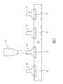
图1至图2B说明传统的倒装芯片封装法。参照图1,裸片(die)10的表面包含焊盘12,其中焊盘12和裸片10中的集成电路相连接。通过一引线接合器(图中未示)的接合头(bond head)15,可在焊盘12上形成凸块(stud bumps)14。当裸片10上的每一接合完成后,引线接合器会施加一个力以剪断对应的接合线,使凸块14附着到焊盘12上。1 to 2B illustrate conventional flip-chip packaging methods. Referring to FIG. 1 , a surface of a die 10 includes
参照图2A,裸片10倒装接合到封装衬底16。典型地,接合工艺包含将凸块14置于封装衬底16的焊盘18上,使焊锡球(solder balls)20位于凸块14和对应的焊盘18之间。接着执行再流(reflow)以熔化焊锡球20,使凸块14能电性连接到焊盘18。Referring to FIG. 2A , die 10 is flip-chip bonded to
图2B是另一倒装芯片接合图,其中裸片10通过各向异性导电膜(Anisotropic Conducting Film,ACF)22,倒装接合到封装衬底16。各向异性导电膜22可将凸块14电性连接到与其对应的焊盘18,而不用提供横向的电路(lateral electrical paths)来短接邻近的凸块14及焊盘18。FIG. 2B is another flip-chip bonding diagram, in which the die 10 is flip-chip bonded to the
使用凸块封装半导体裸片具有降低封装成本的优势特征。然而,传统制造凸块的方法有其缺点。参照图1,欲切断凸块14各自的接合线时,需施加一个力,焊盘12可能会因此与裸片10分层。裸片10要形成互连结构通常需包含低k值的介电材料,而低k值的介电材料极可能会有分层的现象产生。随着集成电路制造技术的发展,所使用的介电材料的k值也越来越低,并因而增加了分层的可能性,因此需要该问题的解决办法。Packaging the semiconductor die using bumps has the advantageous feature of reducing packaging costs. However, conventional methods of making bumps have their drawbacks. Referring to FIG. 1 , when trying to cut off the bonding wires of the
发明内容Contents of the invention
本发明所要解决的技术问题在于提供一种形成封装结构的方法,用以对半导体裸片进行倒装芯片封装。The technical problem to be solved by the present invention is to provide a method for forming a packaging structure for performing flip-chip packaging on semiconductor bare chips.
本发明的另一目的是提供一种集成电路封装结构,该封装结构通过在封装衬底形成凸块,避免对半导体裸片造成损坏。Another object of the present invention is to provide an integrated circuit packaging structure, which avoids damage to the semiconductor die by forming bumps on the packaging substrate.
为了实现上述目的,本发明提供一种形成封装结构的方法,包含提供一半导体裸片、提供一封装衬底、以及形成电性连接于半导体裸片和封装衬底之间的凸块。每一个凸块都具有靠近半导体裸片的第一部分,以及靠近封装衬底的第二部分,其中第一部分的宽度小于第二部分的宽度。To achieve the above object, the present invention provides a method of forming a packaging structure, including providing a semiconductor die, providing a packaging substrate, and forming bumps electrically connected between the semiconductor die and the packaging substrate. Each bump has a first portion proximate to the semiconductor die and a second portion proximate to the packaging substrate, wherein the width of the first portion is smaller than the width of the second portion.
为了实现上述目的,本发明还提供一种形成封装结构的方法,包含提供一半导体裸片、提供一封装衬底、以及形成位于封装衬底的凸块。并将半导体裸片接合到封装衬底,其中凸块电性连接半导体裸片及封装衬底。To achieve the above object, the present invention also provides a method for forming a packaging structure, including providing a semiconductor die, providing a packaging substrate, and forming bumps on the packaging substrate. and bonding the semiconductor die to the package substrate, wherein the bumps are electrically connected to the semiconductor die and the package substrate.
为了实现上述目的,本发明又提供一种集成电路封装结构,包含一半导体裸片、一封装衬底、以及电性连接于半导体裸片和封装衬底之间的凸块。每一个凸块都具有靠近半导体裸片的第一部分,以及靠近封装衬底的第二部分,其中第一部分的宽度小于第二部分的宽度。In order to achieve the above object, the present invention further provides an integrated circuit packaging structure, which includes a semiconductor die, a packaging substrate, and bumps electrically connected between the semiconductor die and the packaging substrate. Each bump has a first portion proximate to the semiconductor die and a second portion proximate to the packaging substrate, wherein the width of the first portion is smaller than the width of the second portion.
为了实现上述目的,本发明又提供一种集成电路封装结构,包含具有顶部表面及位于顶部表面的焊盘的一半导体裸片、一封装衬底、以及电性连接于半导体裸片和封装衬底之间的凸块。凸块以物理方式连接到封装衬底,其中至少一个凸块与其对应的焊盘以物理方式隔离开来。In order to achieve the above object, the present invention further provides an integrated circuit package structure, comprising a semiconductor die having a top surface and a bonding pad located on the top surface, a packaging substrate, and an electrical connection between the semiconductor die and the packaging substrate. bumps between. The bumps are physically connected to the package substrate, with at least one bump being physically isolated from its corresponding pad.
因此,本发明通过先在封装衬底形成凸块,可以消除对半导体裸片造成损坏。Therefore, the present invention can eliminate damage to the semiconductor die by first forming the bumps on the package substrate.
为使本发明和其优点能更明显易懂,下面结合附图进行描述。In order to make the present invention and its advantages more comprehensible, it is described below with reference to the accompanying drawings.
附图说明Description of drawings
图1至图2B说明利用凸块形成集成电路封装结构的传统方法;1 to 2B illustrate a conventional method of forming an integrated circuit package structure using bumps;
图3A至图7是制造本发明的凸块倒装芯片封装结构的一较佳实施例的中间步骤的剖面图;以及3A to 7 are cross-sectional views of intermediate steps in the manufacture of a preferred embodiment of the bump flip-chip package structure of the present invention; and
图8A及图8B示出根据本发明的另一实施例,其中裸片接合到引线框架上。8A and 8B illustrate another embodiment in accordance with the present invention in which a die is bonded to a lead frame.
【主要器件符号说明】【Description of main device symbols】
10:裸片 40:凸块10: bare chip 40: bump
12:焊盘 401:基部12: Pad 401 : Base
14:凸块 402:顶部14: Lug 402 : Top
15:接合头 42:导电指状条15: Bonding head 42: Conductive finger strip
16:封装衬底 50:裸片16: Package substrate 50: Bare chip
18:焊盘 52:焊盘18: Welding pad 52: Welding pad
20:焊锡球 56:各向异性导电膜20: Solder ball 56: Anisotropic conductive film
22:各向异性导电膜 58:导电粒子22: Anisotropic conductive film 58: Conductive particles
30:封装衬底 60:非导电基质30: Package substrate 60: Non-conductive substrate
32:焊盘 62:焊锡球32: Pad 62: Solder ball
34:重布线路 64:模材料34: Rewiring 64: Die material
36:焊盘36: Pad
具体实施方式Detailed ways
以下详细描述本发明较佳实施例的制造与使用。然而应可理解的是,本发明提供诸多可应用的发明概念,其能具体化于各种特定内容中。所描述的特定实施例仅以特定形式说明制造及使用本发明,并非用以限制本发明的范围。The manufacture and use of preferred embodiments of the present invention are described in detail below. It should be appreciated, however, that the present invention provides many applicable inventive concepts, which can be embodied in a wide variety of specific contexts. The specific embodiments described are merely illustrative of specific forms of making and using the invention, and do not limit the scope of the invention.
本发明提供一种新颖的封装结构和形成该封装结构的方法。以下说明一种制造本发明的实施例的中间步骤。在本发明的不同附图和说明性实施例中,相似的元件使用相同的参考编号。The present invention provides a novel packaging structure and a method of forming the packaging structure. An intermediate step in the manufacture of an embodiment of the invention is described below. In the different figures and illustrative embodiments of the invention, similar elements use the same reference numerals.
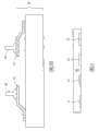
参照图3A,其中示出根据本发明一实施例的一种封装衬底30。在一实施例中,封装衬底30可以是双马来酰亚胺三嗪(Bismaleimide Triazine,BT)衬底、印刷电路板(Print Circuit Board,PCB)衬底、或其它可封装裸片的常用衬底。封装衬底30包含位于顶部表面的焊盘32。焊盘32进一步连接到重布线路(redistribution traces)34而到达底部表面,并和焊盘36相连接。重布线路34也连接封装衬底30顶部表面的焊盘。Referring to FIG. 3A , there is shown a
以使用引线接合器为例,引线接合器会在焊盘32上面形成凸块40。凸块40和引线接合形成的方式相似,不同之处在于引线接合器会使接合线断裂,以让凸块40留在焊盘32上面。在一较佳实施例中,凸块40由具有良好导电及接合性质的金构成,凸块40也可以利用其它金属如铜构成。通过这种凸块形成方法,每一个凸块40包含一基部401(第二部分)及一顶部402(第一部分),基部401宽度W1远大于顶部402宽度W2。Using a wire bonder as an example, the wire bonder will form bumps 40 on
参照图3B的另一实施例,封装衬底30为具有多个导电指状条(conductivefingers)42的引线框架(lead frame),利用类似于前述段落所述的方法,在导电指状条42上面形成凸块40。Referring to another embodiment of FIG. 3B, the
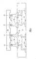
参照图4,其中示出一种半导体裸片50。如本领域公知的技术,半导体裸片形成在半导体晶片(wafer)中,每一个晶片具有多个相同的裸片。当一半导体晶片形成后,该晶片会进行晶片研磨(wafer-grinding)以减少其厚度,并进行晶片测试和晶片切割(sawing)。因此裸片50是优质裸片(Kown-good-die),包含位于顶部表面的焊盘52,其中焊盘52和裸片50内部的集成电路相连接。Referring to FIG. 4, a
参照图5,其中示出裸片50与封装衬底30的接合图。焊盘52与凸块40利用各向异性导电膜56电性连接较佳。各向异性导电膜56包含许多导电粒子(conductive particles)58,导电粒子58彼此之间会被环氧树脂(epoxies)所组成的非导电基质(non-conductive base material)60所隔离开来。在本发明的一个实施例中,各向异性导电膜56会形成在裸片50上。然后通过施加一压力压缩裸片50及封装衬底30,并加热,于是裸片50上的焊盘52通过导电粒子58和凸块40电性连接。各向异性导电膜56有利于使相邻的凸块40及相邻的焊盘32彼此绝缘。Referring to FIG. 5 , a bonding diagram of the
图6与图7示出根据本发明的另一实施例。参照图6,裸片50置于封装衬底30对面,凸块40与焊盘52之间具有焊锡球62。焊锡球62可随着焊剂(Flux)(图中未示)先置于裸片50的焊盘32或凸块40上,接着执行再流而形成如图7所示的结构。经过再流的焊锡球62电性连接焊盘52及凸块40,并应用模材料(molding compound)64以保护该封装结构。6 and 7 show another embodiment according to the present invention. Referring to FIG. 6 , the
图8A与图8B示出根据本发明的又一实施例,其中裸片50和引线框架相接合。参照图8A,裸片50通过一各向异性导电膜56电性连接凸块40。参照图8B,裸片50通过焊锡(如焊锡球)62电性连接凸块40。8A and 8B illustrate yet another embodiment in accordance with the present invention, wherein a
在上述实施例中,封装衬底30与半导体晶片的大小可能类似。在这种情况下,封装衬底30会包含许多子区域,每一个子区域用以接合裸片。不管是整个晶片或是多个彼此隔离的个别裸片,都可接合在封装衬底30上。In the above embodiments, the
本发明的实施例具有以下优点。由于凸块40形成于封装衬底30而非裸片50上,因此在形成凸块的过程中,可避免所施加的力对于裸片50造成的损坏。另一方面,由于封装衬底30不具有低k值的介电材料,因此在凸块形成过程中不容易被损坏。同时,即使是具有k值极低的介电层的裸片,也可以使用本发明的凸块技术。此外,封装裸片的产量也有所提高。因为在传统封装技术中,形成凸块于裸片上的步骤需在裸片和衬底接合之前。然而,在本发明的实施例中,凸块可先形成于衬底上,因此可降低装配工艺的循环时间。Embodiments of the present invention have the following advantages. Since the
虽然本发明及其优点已详细描述,但在不脱离本发明后附的权利要求书的精神和范围的情况下,可以作出各种改变、替代与改进。此外,本发明的应用范围并不局限于上述说明书中的特定实施例的工艺、机器、制造、要素组成、工具、方法及步骤。从本发明的公开范围中,本领域内的任何普通技术人员容易理解,与在此描述的相应的实施例执行大体上相同功能或达到大体上相同的结果的、已存在或以后将被开发的工艺、机械、制造、要素组成、工具、方法或步骤可以根据本发明加以利用。因此,所附权利要求书旨在包含该工艺、机械、制造、要素组成、工具、方法或步骤的范围。Although the present invention and its advantages have been described in detail, various changes, substitutions and improvements can be made without departing from the spirit and scope of the invention as appended claims. In addition, the scope of application of the present invention is not limited to the process, machine, manufacture, component composition, tool, method and steps of the specific embodiments in the above description. From the disclosure scope of the present invention, anyone of ordinary skill in the art can easily understand that the corresponding embodiments described herein perform substantially the same function or achieve substantially the same result, existing or later developed A process, machine, manufacture, composition of elements, means, method or step may be utilized in accordance with the present invention. Accordingly, the appended claims are intended to include within their scope such processes, machines, manufacture, compositions of matter, means, methods or steps.
Claims (22)
Translated fromChineseApplications Claiming Priority (2)
| Application Number | Priority Date | Filing Date | Title |
|---|---|---|---|
| US11/776,387US20090014852A1 (en) | 2007-07-11 | 2007-07-11 | Flip-Chip Packaging with Stud Bumps |
| US11/776,387 | 2007-07-11 |
Publications (2)
| Publication Number | Publication Date |
|---|---|
| CN101345199Atrue CN101345199A (en) | 2009-01-14 |
| CN101345199B CN101345199B (en) | 2010-07-28 |
Family
ID=40247158
Family Applications (1)
| Application Number | Title | Priority Date | Filing Date |
|---|---|---|---|
| CN2007103018933AActiveCN101345199B (en) | 2007-07-11 | 2007-12-20 | Packaging structure and forming method thereof |
Country Status (2)
| Country | Link |
|---|---|
| US (1) | US20090014852A1 (en) |
| CN (1) | CN101345199B (en) |
Cited By (8)
| Publication number | Priority date | Publication date | Assignee | Title |
|---|---|---|---|---|
| CN103050463A (en)* | 2011-10-12 | 2013-04-17 | 联咏科技股份有限公司 | Integrated circuit chip package and glass flip-chip substrate structure applied by same |
| CN103094260A (en)* | 2011-10-31 | 2013-05-08 | 台湾积体电路制造股份有限公司 | Package On Package Devices And Methods Of Packaging Semiconductor Dies |
| CN103187396A (en)* | 2011-12-28 | 2013-07-03 | 美国博通公司 | Semiconductor package with ultra-thin interposer without through-semiconductor vias |
| CN106469699A (en)* | 2015-08-21 | 2017-03-01 | 意法半导体有限公司 | Semiconductor device and manufacturing method thereof |
| CN107768337A (en)* | 2016-08-19 | 2018-03-06 | 联发科技股份有限公司 | Pre-bumped redistribution layer structure and semiconductor package |
| CN110854028A (en)* | 2018-08-20 | 2020-02-28 | 三星电子株式会社 | Flip Chip Bonding Method |
| WO2020215224A1 (en)* | 2019-04-23 | 2020-10-29 | 庆鼎精密电子(淮安)有限公司 | Adapter plate and manufacturing method therefor |
| CN112290338A (en)* | 2019-07-24 | 2021-01-29 | 庆鼎精密电子(淮安)有限公司 | Manufacturing method of adapter plate |
Families Citing this family (8)
| Publication number | Priority date | Publication date | Assignee | Title |
|---|---|---|---|---|
| TW201133745A (en)* | 2009-08-27 | 2011-10-01 | Advanpack Solutions Private Ltd | Stacked bump interconnection structure and semiconductor package formed using the same |
| US8367467B2 (en) | 2010-04-21 | 2013-02-05 | Stats Chippac, Ltd. | Semiconductor method of forming bump on substrate to prevent ELK ILD delamination during reflow process |
| US9230933B2 (en) | 2011-09-16 | 2016-01-05 | STATS ChipPAC, Ltd | Semiconductor device and method of forming conductive protrusion over conductive pillars or bond pads as fixed offset vertical interconnect structure |
| JP5909975B2 (en)* | 2011-10-06 | 2016-04-27 | ソニー株式会社 | Imaging apparatus and electronic apparatus |
| US8912651B2 (en) | 2011-11-30 | 2014-12-16 | Taiwan Semiconductor Manufacturing Company, Ltd. | Package-on-package (PoP) structure including stud bulbs and method |
| CN103151278A (en)* | 2013-02-27 | 2013-06-12 | 南通富士通微电子股份有限公司 | Encapsulation technology |
| TWI696300B (en)* | 2016-03-15 | 2020-06-11 | 晶元光電股份有限公司 | A light-emitting device and the manufacturing method thereof |
| US11444048B2 (en)* | 2017-10-05 | 2022-09-13 | Texas Instruments Incorporated | Shaped interconnect bumps in semiconductor devices |
Family Cites Families (53)
| Publication number | Priority date | Publication date | Assignee | Title |
|---|---|---|---|---|
| US3373481A (en)* | 1965-06-22 | 1968-03-19 | Sperry Rand Corp | Method of electrically interconnecting conductors |
| US4740657A (en)* | 1986-02-14 | 1988-04-26 | Hitachi, Chemical Company, Ltd | Anisotropic-electroconductive adhesive composition, method for connecting circuits using the same, and connected circuit structure thus obtained |
| JP2596960B2 (en)* | 1988-03-07 | 1997-04-02 | シャープ株式会社 | Connection structure |
| US5349495A (en)* | 1989-06-23 | 1994-09-20 | Vlsi Technology, Inc. | System for securing and electrically connecting a semiconductor chip to a substrate |
| WO1996042107A1 (en)* | 1995-06-13 | 1996-12-27 | Hitachi Chemical Company, Ltd. | Semiconductor device, wiring board for mounting semiconductor and method of production of semiconductor device |
| US5874780A (en)* | 1995-07-27 | 1999-02-23 | Nec Corporation | Method of mounting a semiconductor device to a substrate and a mounted structure |
| US5749997A (en)* | 1995-12-27 | 1998-05-12 | Industrial Technology Research Institute | Composite bump tape automated bonding method and bonded structure |
| US5677567A (en)* | 1996-06-17 | 1997-10-14 | Micron Technology, Inc. | Leads between chips assembly |
| JPH1084014A (en)* | 1996-07-19 | 1998-03-31 | Shinko Electric Ind Co Ltd | Manufacture of semiconductor device |
| EP1445995B1 (en)* | 1996-12-27 | 2007-02-14 | Matsushita Electric Industrial Co., Ltd. | Method of mounting an electronic component on a circuit board and system for carrying out the method |
| JPH10270624A (en)* | 1997-03-27 | 1998-10-09 | Toshiba Corp | Chip size package and manufacturing method thereof |
| JP3663938B2 (en)* | 1997-10-24 | 2005-06-22 | セイコーエプソン株式会社 | Flip chip mounting method |
| JP3119230B2 (en)* | 1998-03-03 | 2000-12-18 | 日本電気株式会社 | Resin film and method for connecting electronic components using the same |
| US6332270B2 (en)* | 1998-11-23 | 2001-12-25 | International Business Machines Corporation | Method of making high density integral test probe |
| EP1156520A4 (en)* | 1999-01-29 | 2004-08-25 | Matsushita Electric Industrial Co Ltd | ASSEMBLY METHOD FOR ELECTRONIC COMPONENTS AND THEIR DEVICE |
| JP3346320B2 (en)* | 1999-02-03 | 2002-11-18 | カシオ計算機株式会社 | Semiconductor device and manufacturing method thereof |
| US6410415B1 (en)* | 1999-03-23 | 2002-06-25 | Polymer Flip Chip Corporation | Flip chip mounting technique |
| JP2000323534A (en)* | 1999-05-13 | 2000-11-24 | Sony Corp | Mounting structure of semiconductor element and mounting method thereof |
| JP2001015551A (en)* | 1999-06-29 | 2001-01-19 | Toshiba Corp | Semiconductor device and method of manufacturing the same |
| US6492738B2 (en)* | 1999-09-02 | 2002-12-10 | Micron Technology, Inc. | Apparatus and methods of testing and assembling bumped devices using an anisotropically conductive layer |
| JP2001085470A (en)* | 1999-09-16 | 2001-03-30 | Fujitsu Ltd | Semiconductor device and manufacturing method thereof |
| US6297562B1 (en)* | 1999-09-20 | 2001-10-02 | Telefonaktieboalget Lm Ericsson (Publ) | Semiconductive chip having a bond pad located on an active device |
| JP4403631B2 (en)* | 2000-04-24 | 2010-01-27 | ソニー株式会社 | Manufacturing method of chip-shaped electronic component and manufacturing method of pseudo wafer used for manufacturing the same |
| US6578754B1 (en)* | 2000-04-27 | 2003-06-17 | Advanpack Solutions Pte. Ltd. | Pillar connections for semiconductor chips and method of manufacture |
| US6424031B1 (en)* | 2000-05-08 | 2002-07-23 | Amkor Technology, Inc. | Stackable package with heat sink |
| JP2001332644A (en)* | 2000-05-19 | 2001-11-30 | Sony Corp | Semiconductor device and interposer, and manufacturing method thereof |
| JP4609617B2 (en)* | 2000-08-01 | 2011-01-12 | 日本電気株式会社 | Semiconductor device mounting method and mounting structure |
| JP3822040B2 (en)* | 2000-08-31 | 2006-09-13 | 株式会社ルネサステクノロジ | Electronic device and manufacturing method thereof |
| DE10163799B4 (en)* | 2000-12-28 | 2006-11-23 | Matsushita Electric Works, Ltd., Kadoma | Semiconductor chip mounting substrate and method of manufacturing such a mounting substrate |
| US20020093108A1 (en)* | 2001-01-15 | 2002-07-18 | Grigorov Ilya L. | Flip chip packaged semiconductor device having double stud bumps and method of forming same |
| US20020098620A1 (en)* | 2001-01-24 | 2002-07-25 | Yi-Chuan Ding | Chip scale package and manufacturing method thereof |
| US6940178B2 (en)* | 2001-02-27 | 2005-09-06 | Chippac, Inc. | Self-coplanarity bumping shape for flip chip |
| US7242099B2 (en)* | 2001-03-05 | 2007-07-10 | Megica Corporation | Chip package with multiple chips connected by bumps |
| US20020151164A1 (en)* | 2001-04-12 | 2002-10-17 | Jiang Hunt Hang | Structure and method for depositing solder bumps on a wafer |
| FR2826153B1 (en)* | 2001-06-14 | 2004-05-28 | A S K | METHOD FOR CONNECTING A CHIP TO AN ANTENNA OF A RADIO FREQUENCY IDENTIFICATION DEVICE OF THE CONTACTLESS CHIP CARD TYPE |
| TW508987B (en)* | 2001-07-27 | 2002-11-01 | Phoenix Prec Technology Corp | Method of forming electroplated solder on organic printed circuit board |
| US6550666B2 (en)* | 2001-08-21 | 2003-04-22 | Advanpack Solutions Pte Ltd | Method for forming a flip chip on leadframe semiconductor package |
| US20030116346A1 (en)* | 2001-12-21 | 2003-06-26 | Forster James Allam | Low cost area array probe for circuits having solder-ball contacts are manufactured using a wire bonding machine |
| JP4238124B2 (en)* | 2003-01-07 | 2009-03-11 | 積水化学工業株式会社 | Curable resin composition, adhesive epoxy resin paste, adhesive epoxy resin sheet, conductive connection paste, conductive connection sheet, and electronic component assembly |
| TWI231023B (en)* | 2003-05-27 | 2005-04-11 | Ind Tech Res Inst | Electronic packaging with three-dimensional stack and assembling method thereof |
| JP4175197B2 (en)* | 2003-06-27 | 2008-11-05 | 株式会社デンソー | Flip chip mounting structure |
| KR100604334B1 (en)* | 2003-11-25 | 2006-08-08 | (주)케이나인 | Flip Chip Bondig Method for Enhancing the Performance of Connection in Flip Chip Packaging Process |
| JP2005191541A (en)* | 2003-12-05 | 2005-07-14 | Seiko Epson Corp | Semiconductor device, semiconductor chip, semiconductor device manufacturing method, and electronic apparatus |
| US7176043B2 (en)* | 2003-12-30 | 2007-02-13 | Tessera, Inc. | Microelectronic packages and methods therefor |
| JP4776188B2 (en)* | 2004-08-03 | 2011-09-21 | 古河電気工業株式会社 | Semiconductor device manufacturing method and wafer processing tape |
| US8035225B2 (en)* | 2004-12-28 | 2011-10-11 | Panasonic Corporation | Semiconductor chip assembly and fabrication method therefor |
| US7598600B2 (en)* | 2005-03-30 | 2009-10-06 | Stats Chippac Ltd. | Stackable power semiconductor package system |
| JP4535002B2 (en)* | 2005-09-28 | 2010-09-01 | Tdk株式会社 | Semiconductor IC-embedded substrate and manufacturing method thereof |
| KR100719905B1 (en)* | 2005-12-29 | 2007-05-18 | 삼성전자주식회사 | Sn-based solder alloys and semiconductor devices using the same |
| JP4863746B2 (en)* | 2006-03-27 | 2012-01-25 | 富士通株式会社 | Semiconductor device and manufacturing method thereof |
| US7713782B2 (en)* | 2006-09-22 | 2010-05-11 | Stats Chippac, Inc. | Fusible I/O interconnection systems and methods for flip-chip packaging involving substrate-mounted stud-bumps |
| US8174119B2 (en)* | 2006-11-10 | 2012-05-08 | Stats Chippac, Ltd. | Semiconductor package with embedded die |
| US7759951B2 (en)* | 2007-05-29 | 2010-07-20 | Touchdown Technologies, Inc. | Semiconductor testing device with elastomer interposer |
- 2007
- 2007-07-11USUS11/776,387patent/US20090014852A1/ennot_activeAbandoned
- 2007-12-20CNCN2007103018933Apatent/CN101345199B/enactiveActive
Cited By (16)
| Publication number | Priority date | Publication date | Assignee | Title |
|---|---|---|---|---|
| CN103050463B (en)* | 2011-10-12 | 2017-06-09 | 联咏科技股份有限公司 | Glass Flip-Chip Substrate Structure for Integrated Circuit Chip Packages and Applications |
| CN103050463A (en)* | 2011-10-12 | 2013-04-17 | 联咏科技股份有限公司 | Integrated circuit chip package and glass flip-chip substrate structure applied by same |
| CN103094260A (en)* | 2011-10-31 | 2013-05-08 | 台湾积体电路制造股份有限公司 | Package On Package Devices And Methods Of Packaging Semiconductor Dies |
| CN103187396A (en)* | 2011-12-28 | 2013-07-03 | 美国博通公司 | Semiconductor package with ultra-thin interposer without through-semiconductor vias |
| US9013041B2 (en) | 2011-12-28 | 2015-04-21 | Broadcom Corporation | Semiconductor package with ultra-thin interposer without through-semiconductor vias |
| CN113257766A (en)* | 2015-08-21 | 2021-08-13 | 意法半导体有限公司 | Semiconductor device and method for manufacturing the same |
| US10269583B2 (en) | 2015-08-21 | 2019-04-23 | Stmicroelectronics Pte Ltd | Semiconductor die attachment with embedded stud bumps in attachment material |
| CN106469699A (en)* | 2015-08-21 | 2017-03-01 | 意法半导体有限公司 | Semiconductor device and manufacturing method thereof |
| CN107768337A (en)* | 2016-08-19 | 2018-03-06 | 联发科技股份有限公司 | Pre-bumped redistribution layer structure and semiconductor package |
| CN110854028A (en)* | 2018-08-20 | 2020-02-28 | 三星电子株式会社 | Flip Chip Bonding Method |
| WO2020215224A1 (en)* | 2019-04-23 | 2020-10-29 | 庆鼎精密电子(淮安)有限公司 | Adapter plate and manufacturing method therefor |
| CN112514065A (en)* | 2019-04-23 | 2021-03-16 | 庆鼎精密电子(淮安)有限公司 | Adapter plate and manufacturing method thereof |
| TWI740144B (en)* | 2019-04-23 | 2021-09-21 | 大陸商慶鼎精密電子(淮安)有限公司 | Adapter board and method for making the same |
| US11665820B2 (en) | 2019-04-23 | 2023-05-30 | Qing Ding Precision Electronics (Huaian) Co., Ltd | Adapter board and method for making adapter board |
| CN112514065B (en)* | 2019-04-23 | 2024-05-14 | 庆鼎精密电子(淮安)有限公司 | Adapter plate and manufacturing method thereof |
| CN112290338A (en)* | 2019-07-24 | 2021-01-29 | 庆鼎精密电子(淮安)有限公司 | Manufacturing method of adapter plate |
Also Published As
| Publication number | Publication date |
|---|---|
| CN101345199B (en) | 2010-07-28 |
| US20090014852A1 (en) | 2009-01-15 |
Similar Documents
| Publication | Publication Date | Title |
|---|---|---|
| CN101345199A (en) | Packaging structure and forming method thereof | |
| US12119320B2 (en) | Chip package structure with bump | |
| US8823180B2 (en) | Package on package devices and methods of packaging semiconductor dies | |
| KR102450822B1 (en) | Manufacturing method for semiconductor device | |
| TWI529886B (en) | Packages, methods of packaging a device and package on package devices | |
| TWI496259B (en) | Flip chip package assembly and process for making same | |
| US20090071699A1 (en) | Packaging substrate structure and method for manufacturing the same | |
| US20060043603A1 (en) | Low temperature PB-free processing for semiconductor devices | |
| CN109390306A (en) | Electronic package | |
| US9627325B2 (en) | Package alignment structure and method of forming same | |
| TWI381509B (en) | Semiconductor package and method for manufacturing the same | |
| US8008765B2 (en) | Semiconductor package having adhesive layer and method of manufacturing the same | |
| CN105702648A (en) | Chip package structure and manufacturing method thereof | |
| KR20190136459A (en) | Method of stacking multiple semiconductor dies and semiconductor package including stacked dies | |
| JP2003100948A (en) | Semiconductor device and manufacturing method thereof | |
| US20180204814A1 (en) | Method for preparing a semiconductor package | |
| CN100394566C (en) | Semiconductor package and method of manufacturing the same | |
| TWI763747B (en) | Semiconductor device and method of manufacturing the same | |
| TWI651827B (en) | Substrate-free package structure | |
| TWI590349B (en) | Chip package and chip packaging process | |
| CN101527292B (en) | Chip packaging structure | |
| US20170084562A1 (en) | Package structure, chip structure and fabrication method thereof | |
| KR20130042938A (en) | Semiconductor chip, semiconductor package having the same, and method of fabricating stack type semiconductor package | |
| Essig et al. | High efficient mid power modules by next generation chip embedding technology | |
| TWI418276B (en) | Method for making package substrate with wingless conductive bump |
Legal Events
| Date | Code | Title | Description |
|---|---|---|---|
| C06 | Publication | ||
| PB01 | Publication | ||
| C10 | Entry into substantive examination | ||
| SE01 | Entry into force of request for substantive examination | ||
| C14 | Grant of patent or utility model | ||
| GR01 | Patent grant |