CN101345023B - Control method, display panel and electronic system - Google Patents
Control method, display panel and electronic systemDownload PDFInfo
- Publication number
- CN101345023B CN101345023BCN2007101226838ACN200710122683ACN101345023BCN 101345023 BCN101345023 BCN 101345023BCN 2007101226838 ACN2007101226838 ACN 2007101226838ACN 200710122683 ACN200710122683 ACN 200710122683ACN 101345023 BCN101345023 BCN 101345023B
- Authority
- CN
- China
- Prior art keywords
- terminal
- voltage
- period
- during
- transistor
- Prior art date
- Legal status (The legal status is an assumption and is not a legal conclusion. Google has not performed a legal analysis and makes no representation as to the accuracy of the status listed.)
- Active
Links
Images


Landscapes
- Control Of Indicators Other Than Cathode Ray Tubes (AREA)
- Control Of El Displays (AREA)
Abstract
Description
Translated fromChinese技术领域technical field
本发明涉及一种控制方法,特别是涉及一种控制显示面板的控制方法。The present invention relates to a control method, in particular to a control method for controlling a display panel.
背景技术Background technique
由于显像管具有画质优良和价格低廉的特点,故一直被采用为电视和计算机的显示器。然而,随着科技的进步,陆续开发出新的平面显示器。平面显示器的主要优点在于,当具有大尺寸的显示面板时,平面显示器的总体积并不会因此而有显著的改变。一般而言,平面显示器包含液晶显示器、等离子显示器、场发射显示器以及电发光显示器。Due to its excellent picture quality and low price, picture tubes have been used as monitors for televisions and computers. However, with the advancement of technology, new flat panel displays have been developed one after another. The main advantage of the flat panel display is that the overall volume of the flat panel display does not significantly change when having a large size display panel. In general, flat panel displays include liquid crystal displays, plasma displays, field emission displays, and electroluminescence displays.
电发光显示器包括有机发光二极管(Organic Light Emitting Diode;OLED)显示器以及高分子发光二极管(Polymeric Light Emitting Diode;PLED)显示器。按照驱动方式可将有机发光二极管区分为被动矩阵式有机发光二极管(PM-OLED)及主动矩阵式有机发光二极管(AM-OLED)。AMOLED显示器具有体积薄、重量轻、自发光的高发光效率以及低驱动电压等优点,且具有广视角、高对比、高应答速度、全彩化及可挠曲化的特性。Electroluminescence displays include Organic Light Emitting Diode (OLED) displays and Polymeric Light Emitting Diode (PLED) displays. Organic light emitting diodes can be classified into passive matrix organic light emitting diodes (PM-OLED) and active matrix organic light emitting diodes (AM-OLED) according to their driving methods. AMOLED displays have the advantages of thin size, light weight, high self-luminous luminous efficiency and low driving voltage, and have the characteristics of wide viewing angle, high contrast, high response speed, full color and flexibility.
AMOLED显示器是由电流所驱动的。AMOLED显示器的每一像素单元具有一驱动晶体管以及一OLED。驱动晶体管提供一驱动电流给OLED,使其发光。OLED所发出的光线的强度取决于驱动电流的大小。然而,由于制造过程的影响,将造成不同像素单元里的驱动晶体管可能具有不同的阈电压(threshold voltage),因而造成像素单元呈现错误的亮度。AMOLED displays are driven by electric current. Each pixel unit of the AMOLED display has a driving transistor and an OLED. The driving transistor provides a driving current to the OLED to make it emit light. The intensity of the light emitted by the OLED depends on the magnitude of the driving current. However, due to the influence of the manufacturing process, the driving transistors in different pixel units may have different threshold voltages, thus causing the pixel units to display wrong brightness.
发明内容Contents of the invention
本发明提供一种控制方法,用来控制一显示面板。显示面板包括一像素单元。像素单元耦接一数据线,并具有一电容、一晶体管以及一发光元件。电容的一第一端耦接数据线,其一第二端耦接晶体管。本发明的控制方法包括:在一第一期间,增加该第一端的电压并降低该第二端的电压;在该第一期间之后的一第二期间,控制该第一端及第二端的电压;在该第二期间之后的一第三期间,根据该电容所储存的电压,点亮该发光元件,其中在该第三期间,该数据线的电压电位维持不变。The invention provides a control method for controlling a display panel. The display panel includes a pixel unit. The pixel unit is coupled to a data line and has a capacitor, a transistor and a light emitting element. A first end of the capacitor is coupled to the data line, and a second end of the capacitor is coupled to the transistor. The control method of the present invention includes: increasing the voltage of the first terminal and decreasing the voltage of the second terminal during a first period; controlling the voltages of the first terminal and the second terminal during a second period after the first period ; In a third period following the second period, according to the voltage stored in the capacitor, the light-emitting element is turned on, wherein in the third period, the voltage potential of the data line remains unchanged.
本发明另提供一种显示面板,具有一像素单元以及一阴极开关。像素单元包括,一电容、一晶体管以及一发光元件。阴极开关耦接发光元件。电容具有一第一端以及一第二端。电容的第一端耦接一数据线。在一第一期间,电容的第一端的电压会被增加而电容的第二端的电压会被降低。在第一期间之后的一第二期间,控制电容的第一及第二端的电压。晶体管耦接电容的第二端。发光元件在第二期间之后的一第三期间,根据电容所储存的电压而发光。在第三期间,数据线的电压电位维持不变。The present invention further provides a display panel, which has a pixel unit and a cathode switch. The pixel unit includes a capacitor, a transistor and a light emitting element. The cathode switch is coupled to the light emitting element. The capacitor has a first terminal and a second terminal. The first end of the capacitor is coupled to a data line. During a first period, the voltage at the first terminal of the capacitor is increased and the voltage at the second terminal of the capacitor is decreased. During a second period following the first period, the voltages of the first and second terminals of the capacitor are controlled. The transistor is coupled to the second end of the capacitor. The light emitting element emits light according to the voltage stored in the capacitor during a third period after the second period. During the third period, the voltage level of the data line remains unchanged.
本发明还提供一种电子系统,包括一显示面板以及一电源转换器。电源转换器用来提供一电源信号给显示面板。显示面板具有一像素单元以及一阴极开关。像素单元包括,一电容、一晶体管以及一发光元件。阴极开关耦接发光元件。电容具有一第一端以及一第二端。电容的第一端耦接一数据线。在一第一期间,电容的第一端的电压会被增加而电容的第二端的电压会被降低。在第一期间之后的一第二期间,控制电容的第一及第二端的电压。晶体管耦接电容的第二端。发光元件在第二期间之后的一第三期间,根据电容所储存的电压而发光。在第三期间,数据线的电压电位维持不变。The invention also provides an electronic system including a display panel and a power converter. The power converter is used to provide a power signal to the display panel. The display panel has a pixel unit and a cathode switch. The pixel unit includes a capacitor, a transistor and a light emitting element. The cathode switch is coupled to the light emitting element. The capacitor has a first terminal and a second terminal. The first end of the capacitor is coupled to a data line. During a first period, the voltage at the first terminal of the capacitor is increased and the voltage at the second terminal of the capacitor is decreased. During a second period following the first period, the voltages of the first and second terminals of the capacitor are controlled. The transistor is coupled to the second terminal of the capacitor. The light emitting element emits light according to the voltage stored in the capacitor during a third period after the second period. During the third period, the voltage potential of the data line remains unchanged.
为使得本发明的上述和其它目的、特征、和优点能更明显易懂,下文特举出较佳实施例,并配合附图作详细说明如下:In order to make the above-mentioned and other objects, features, and advantages of the present invention more comprehensible, preferred embodiments are listed below, and are described in detail in conjunction with the accompanying drawings as follows:
附图说明Description of drawings
图1为本发明的电子系统的示意图。FIG. 1 is a schematic diagram of the electronic system of the present invention.
图2为本发明的显示面板的示意图。FIG. 2 is a schematic diagram of a display panel of the present invention.
图3为本发明的像素单元的示意图。FIG. 3 is a schematic diagram of a pixel unit of the present invention.
图4为本发明的控制方法的一可能实施例。Fig. 4 is a possible embodiment of the control method of the present invention.
图5为本发明的控制方法的另一可能实施例。Fig. 5 is another possible embodiment of the control method of the present invention.
附图标记说明如下:The reference signs are explained as follows:
100:电子系统;110:电源转换器;100: electronic system; 110: power converter;
120:显示面板;122:栅极驱动器;120: display panel; 122: gate driver;
124:源极驱动器;126:阴极开关;124: source driver; 126: cathode switch;
128:控制器;312、322:电容;128: controller; 312, 322: capacitor;
316、326:发光元件;330:充电开关;316, 326: light emitting elements; 330: charging switch;
340:电源开关;P11~Pmn:像素单元;340: power switch; P11 ~Pmn : pixel unit;
S1~Sn:扫描线;D1~Dm:数据线;S1 ~Sn : scanning lines; D1 ~Dm : data lines;
STV:启始信号;SPW:电源信号;STV: start signal; SPW : power signal;
SPre:充电信号;SEL_PW:驱动信号;SPre : charging signal; SEL_PW : driving signal;
SEMIT:发光信号;T41~T46、T51~T57:期间;SEMIT : light emitting signal; T41 ~T46 , T51 ~T57 : period;
SDATA:数据信号;PVDD、PVEE:电压信号;SDATA : data signal; PVDD, PVEE: voltage signal;
SSCAN1、SSCAN2:扫描信号;SSCAN1 , SSCAN2 : scanning signal;
Q1~Q3、314、318、324、328:晶体管。Q1 -Q3 , 314, 318, 324, 328: transistors.
具体实施方式Detailed ways
图1为本发明的电子系统的示意图。本发明的电子系统可为个人数字助理(PDA)、移动电话(cellular phone)、笔记本计算机或是台式计算机。如图所示,电子系统100包括电源转换器110以及显示面板120。电源转换器110提供电源信号SPW给显示面板120,使其呈现画面。在一可能实施例中,电源转换器110可将一交流信号转换成一直流信号,以作为电源信号SPW。在其它实施例中,电源转换器110可转换一直流信号的电压电位,以产生电源信号SPW。FIG. 1 is a schematic diagram of the electronic system of the present invention. The electronic system of the present invention can be a personal digital assistant (PDA), a cellular phone, a notebook computer or a desktop computer. As shown in the figure, the
图2为本发明的显示面板的示意图。如图所示,显示面板120包括,栅极驱动器122、源极驱动器124、阴极开关126、控制器128以及像素单元P11~Pmn。栅极驱动器122通过扫描线S1~Sn,提供扫描信号给像素单元P11~Pmn。源极驱动器124通过数据线D1~Dm,提供数据信号给像素单元P11~Pmn。阴极开关126耦接像素单元P11~Pmn里的发光元件。FIG. 2 is a schematic diagram of a display panel of the present invention. As shown in the figure, the
在本实施例中,阴极开关126具有晶体管Q1~Q3。晶体管Q1~Q3并联在一起,并且其栅极均接收发光信号SEMIT。本发明并不限制阴极开关126里的晶体管数量,在其它实施例中,阴极开关126可仅具有单一晶体管。控制器128提供像素单元P11~Pmn所需的控制信号或电压信号。在本实施例中,控制器128是根据像素单元P11~Pmn的内部结构,提供一个或多个控制信号。在其它实施例中,可将控制器128整合在栅极驱动器122或在源极驱动器124之中。In this embodiment, the
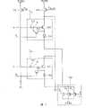
图3为本发明的像素单元的示意图。由于像素单元P11~Pmn的内部结构均相同,故仅显示像素单元P11及P12的内部结构。如图所示,像素单元P11具有电容312、晶体管314、318以及发光元件316。晶体管318的栅极耦接扫描线S1。在其它实施例中,晶体管318可为N型。像素单元P12具有电容322、晶体管324、328以及发光元件326。晶体管328的栅极耦接扫描线S2。FIG. 3 is a schematic diagram of a pixel unit of the present invention. Since the internal structures of the pixel units P11 -Pmn are the same, only the internal structures of the pixel units P11 and P12 are shown. As shown in the figure, the pixel unit P11 has a
充电开关330为一P型晶体管,其源极接收电压信号PVDD,其漏极耦接电容312、322以及数据线D1,其栅极接收充电信号SPre。电源开关340为一P型晶体管,其源极接收电压信号PVDD,其漏极耦接晶体管314及324,其栅极接收驱动信号SEL_PW。在本实施例中,充电开关330及电源开关340被设置在显示面板上,其所需的信号(如电压信号PVDD、充电信号SPre、驱动信号SEL_PW)均来自控制器128(如图2所示)。在其它实施例中,可省略电源开关340,或是以N型晶体管取代电源开关340。当电源开关340被省略时,则晶体管314及324的源极直接接收电压信号PVDD。The charging
另外,如图所示,阴极开关126耦接发光元件316及326。发光元件316及326均为有机发光二极管(OLED),其阴极耦接晶体管Q1~Q3的漏极。晶体管Q1~Q3的源极接收电压信号PVEE,其栅极接收发光信号SEMIT。在本实施例中,发光信号SEMIT是由图2所示的控制器128所提供的,并且电压信号PVEE的电位低于电压信号PVDD的电位。In addition, as shown, the
图4为本发明的控制方法的一可能实施例。本发明的控制方法除了可应用在如图3所示的像素单元,也可应用在其它结构的像素单元。请搭配图2和如3,以下将说明本发明的一可能控制方法。在本实施例中,假设显示面板呈现一画面(frame)的时间为16.6ms,因此启始信号STV的周期为16.63ms。Fig. 4 is a possible embodiment of the control method of the present invention. In addition to being applicable to the pixel unit shown in FIG. 3 , the control method of the present invention can also be applied to pixel units with other structures. With reference to FIG. 2 and FIG. 3 , a possible control method of the present invention will be described below. In this embodiment, it is assumed that the time for the display panel to present a frame is 16.6 ms, so the period of the start signal STV is 16.63 ms.
在期间T41内,驱动信号SEL_PW为高电位,因此不导通电源开关340。由于扫描线S1上的扫描信号SSCAN1为低电位,而发光信号SEMIT为高电位,故导通晶体管318、Q1~Q3。因此,降低节点B的电压。由于充电信号SPre为低电位,故增加节点A的电压。During the periodT41 , the driving signal SEL_PW is at a high potential, so the
在期间T42内,扫描信号SSCAN1为高电位,故不导通晶体管318,因此,节点B的电压维持在一固定值。此时驱动信号SEL_PW为低电位,故电源开关340被导通。由于电源开关340为导通状态,因此晶体管314也为导通状态。由于源极驱动器124通过数据线D1提供数据信号SDATA,故将降低节点A的电压。此时,节点A的电压与数据信号SDATA有关。During the periodT42 , the scan signal SSCAN1 is at a high potential, so the
在期间T43内,发光信号SEMIT为低电位,故不导通晶体管Q1~Q3。充电信号SPre为高电位,故不导通充电开关330。由于数据线D1并未提供数据信号SDATA,故节点A的电压将维持在一固定值。由于扫描信号SSCAN1及电源信号SEL_PW均为低电位,故晶体管318以及电源开关340将被导通。因此,增加节点B的电压。此时,节点B的电压不但与晶体管314的阈电压有关且与PVDD有关。During the period T43 , the light emitting signal SEMIT is at a low potential, so the transistors Q1 -Q3 are not turned on. The charging signal SPre is at a high potential, so the charging
在本实施例中,晶体管314为一驱动晶体管,其根据电容312所储存的电压而产生一驱动电流。发光元件316根据驱动电流而发光。然而,受到制造过程的影响,可能造成不同像素单元里的驱动元件具有不同的阈电压。因此,在期间T43内,使得节点B的电压与对应的驱动晶体管的阈电压有关,因而补偿了不同的驱动元件具有不同的阈电压的问题,并且可补偿不同像素单元接收到不同电位的电压信号PVDD。In this embodiment, the
在期间T44内,扫描信号SSCAN2为高电位,故不导通晶体管328,因此,节点D的电压维持在一固定值。由于驱动信号SEL_PW为低电位,故可导通电源开关340,进而导通晶体管324。此时,由于源极驱动器124通过数据线D1提供数据信号SDATA,故节点C的电压可根据数据信号SDATA而被增加或减少。因此,节点C的电压与数据信号SDATA有关。During the periodT44 , the scan signal SSCAN2 is at a high potential, so the
在期间T45内,发光信号SEMIT为低电位,故不导通晶体管Q1~Q3。充电信号SPre为高电位,故不导通充电开关330。由于数据线D1并未提供数据信号SDATA,故节点C的电压将维持在一固定值。During the period T45 , the light emitting signal SEMIT is at a low potential, so the transistors Q1 -Q3 are not turned on. The charging signal SPre is at a high potential, so the charging
由于扫描信号SSCAN2及电源信号SEL_PW均为低电位,故晶体管328被导通以及电源开关340将被导通。因此,增加节点D的电压。此时,节点D的电压不但与晶体管324的阈电压有关且与PVDD有关。Since the scan signal SSCAN2 and the power signal SEL_PW are both low, the
在期间T46内,充电信号SPre、扫描信号SSCAN1、SSCAN2均为高电位,故不导通充电开关330、晶体管318、328。由于发光信号SEMIT为高电位,而驱动信号SEL_PW为低电位,故使晶体管314及324运行在饱和区。晶体管314及324分别根据电容312及322所储存的电压而产生驱动电流。发光元件316及326分别根据晶体管314及324所产生的驱动电流而发光。当驱动电流愈大时,发光元件所产生的光线强度也愈强。另外,特别需注意的是,在期间T46内,数据信号SDATA的电压电位维持不变。在一可能实施例中,数据信号SDATA的电压电位可维持在接地电位(Ground)。During the period T46 , the charging signal SPre , the scanning signals SSCAN1 , and SSCAN2 are all high potentials, so the charging
图5为本发明的控制方法的另一可能实施例。请搭配图2和图3,以下将针对电源开关340被省略,晶体管314的源极接收电压信号PVDD的情况,说明本发明的一可能控制方法。由于晶体管314的源极接收电压信号PVDD,故晶体管314保持在导通状态。在本实施例中,假设显示面板呈现一画面(frame)的时间为16.6ms,因此启始信号STV的周期为16.63ms。Fig. 5 is another possible embodiment of the control method of the present invention. Please refer to FIG. 2 and FIG. 3 , and a possible control method of the present invention will be described below for the case where the
在期间T51内,由于充电信号SPre以及扫描线S1上的扫描信号SSCAN1为低电位,发光信号SEMIT为高电位,故充电开关330、晶体管318、Q1~Q3均被导通。因此,增加节点A的电压并降低节点B的电压使其维持在一固定值。During the periodT51 , since the charging signal SPre and the scanning signal SSCAN1 on the scanning lineS1 are at low potential, and the light emitting signal SEMIT is at a high potential, the charging
在期间T52内,发光信号SEMIT为低电位,故不导通晶体管Q1~Q3。而充电信号SPre为高电位,故不导通充电开关330。因此,节点A的电压维持在一固定值。由于扫描信号SSCAN1为低电位,故晶体管318仍被导通。因此,增加节点B的电压。此时,节点B的电压与晶体管314的阈电压有关,因此,可补偿因制造过程的关系,而造成不同的驱动元件具有不同的阈电压的问题。During the period T52 , the light emitting signal SEMIT is at a low potential, so the transistors Q1 -Q3 are not turned on. The charging signal SPre is at a high potential, so the charging
另外,若电压信号PVDD是由控制器128所提供时,当像素单元离控制器128愈远时,其所接收到的电压信号PVDD可能会下降。然而借助于本发明的控制方法,在期间T52内,可使得节点B的电压还与电压信号PVDD有关,故可补偿不同像素单元接收到不同电位的电压信号PVDD。In addition, if the voltage signal PVDD is provided by the
在期间T53的第一期间内,由于扫描信号SSCAN1为低电位,故导通晶体管318。因此,增加节点B的电压。在期间T53的第二期间内,由于扫描信号SSCAN1为高电位,故不导通晶体管318。因此,节点B的电压维持在一固定值。当源极驱动器124通过数据线D1提供数据信号SDATA,则降低节点A的电压。此时,节点A的电压与数据信号SDATA有关。During the first period of the periodT53 , since the scan signal SSCAN1 is at a low potential, the
在期间T54的第一期间内,由于充电信号SPre以及扫描线S2上的扫描信号SSCAN2为高电位,发光信号SEMIT为低电位,故充电开关330、晶体管328、Q1~Q3均不被导通。因此,节点D的电压维持在一固定值。由于数据线D1并未提供数据信号SDATA,故节点C的电压将维持在一固定值。在期间T54的第二期间内,由于充电信号SPre以及扫描线S2上的扫描信号SSCAN2为低电位,而发光信号SEMIT为高电位,故充电开关330、晶体管328、Q1~Q3均被导通。因此,降低节点D的电压使其维持在一固定值。由于数据线D1并未提供数据信号SDATA,故节点C的电压将维持在一固定值。During the first period ofT54 , since the charging signal SPre and the scanning signalS SCAN2on the scanning line S2 are at high potential, and the light emitting signal SEMIT is at low potential, the charging
在期间T55内,发光信号SEMIT为低电位,故不导通晶体管Q1~Q3。而充电信号SPre为高电位,故不导通充电开关330。因此,节点C的电压维持在一固定值。由于扫描信号SSCAN2为低电位,故晶体管328仍被导通。因此,增加节点D的电压。此时,节点D的电压除了与晶体管324的阈电压有关,还与电压信号PVDD有关。During the period T55 , the light emitting signal SEMIT is at a low potential, so the transistors Q1 -Q3 are not turned on. The charging signal SPre is at a high potential, so the charging
在期间T56的第一期间内,由于扫描信号SSCAN2为低电位,故导通晶体管328。因此,增加节点D的电压。在期间T56的第二期间内,由于扫描信号SSCAN2为高电位,故不导通晶体管328。因此,节点D的电压维持在一固定值。当源极驱动器124通过数据线D1提供数据信号SDATA,则降低或增加节点C的电压。此时,节点C的电压与数据信号SDATA有关。During the first period of the periodT56 , since the scan signal SSCAN2 is low, the
在期间T57内,充电信号SPre、扫描信号SSCAN1、SSCAN2均为高电位,故不导通充电开关330、晶体管318、328。由于发光信号SEMIT为高电位,故晶体管314及324运行在饱和区。晶体管314及324分别根据电容312及322所储存的电压而产生驱动电流。发光元件316及326分别根据晶体管314及324所产生的驱动电流而发光。当驱动电流愈大时,发光元件所产生的光线强度也愈强。另外,特别需注意的是,在期间T57内,数据信号SDATA的电压电位维持不变。During the period T57 , the charging signal SPre , the scanning signals SSCAN1 , and SSCAN2 are all high potentials, so the charging
虽然本发明已以较佳实施例揭露如上,但是其并不是用来限定本发明,任何熟悉该技术的人,在不脱离本发明的精神和范围的条件下,应该可以作一些更动和润饰,因此本发明的保护范围当视后附的权利要求所界定的为准。Although the present invention has been disclosed above with preferred embodiments, it is not intended to limit the present invention, and anyone familiar with the technology should be able to make some changes and modifications without departing from the spirit and scope of the present invention. , so the scope of protection of the present invention shall prevail as defined by the appended claims.
Claims (9)
Translated fromChinesePriority Applications (1)
| Application Number | Priority Date | Filing Date | Title |
|---|---|---|---|
| CN2007101226838ACN101345023B (en) | 2007-07-12 | 2007-07-12 | Control method, display panel and electronic system |
Applications Claiming Priority (1)
| Application Number | Priority Date | Filing Date | Title |
|---|---|---|---|
| CN2007101226838ACN101345023B (en) | 2007-07-12 | 2007-07-12 | Control method, display panel and electronic system |
Publications (2)
| Publication Number | Publication Date |
|---|---|
| CN101345023A CN101345023A (en) | 2009-01-14 |
| CN101345023Btrue CN101345023B (en) | 2012-01-25 |
Family
ID=40247019
Family Applications (1)
| Application Number | Title | Priority Date | Filing Date |
|---|---|---|---|
| CN2007101226838AActiveCN101345023B (en) | 2007-07-12 | 2007-07-12 | Control method, display panel and electronic system |
Country Status (1)
| Country | Link |
|---|---|
| CN (1) | CN101345023B (en) |
Families Citing this family (1)
| Publication number | Priority date | Publication date | Assignee | Title |
|---|---|---|---|---|
| JP5961125B2 (en)* | 2013-02-26 | 2016-08-02 | 株式会社ジャパンディスプレイ | Display device and electronic device |
Citations (4)
| Publication number | Priority date | Publication date | Assignee | Title |
|---|---|---|---|---|
| CN1716367A (en)* | 2004-06-29 | 2006-01-04 | 三星Sdi株式会社 | Light emitting display and driving method thereof |
| CN1742309A (en)* | 2003-01-24 | 2006-03-01 | 皇家飞利浦电子股份有限公司 | Active matrix display devices |
| CN1851794A (en)* | 2005-04-22 | 2006-10-25 | 中国科学院长春光学精密机械与物理研究所 | Organic electroluminescent display driving method |
| CN1953023A (en)* | 2005-10-18 | 2007-04-25 | 株式会社半导体能源研究所 | Display device and driving method thereof |
- 2007
- 2007-07-12CNCN2007101226838Apatent/CN101345023B/enactiveActive
Patent Citations (4)
| Publication number | Priority date | Publication date | Assignee | Title |
|---|---|---|---|---|
| CN1742309A (en)* | 2003-01-24 | 2006-03-01 | 皇家飞利浦电子股份有限公司 | Active matrix display devices |
| CN1716367A (en)* | 2004-06-29 | 2006-01-04 | 三星Sdi株式会社 | Light emitting display and driving method thereof |
| CN1851794A (en)* | 2005-04-22 | 2006-10-25 | 中国科学院长春光学精密机械与物理研究所 | Organic electroluminescent display driving method |
| CN1953023A (en)* | 2005-10-18 | 2007-04-25 | 株式会社半导体能源研究所 | Display device and driving method thereof |
Non-Patent Citations (1)
| Title |
|---|
| JP特开2005-346025A 2005.12.15 |
Also Published As
| Publication number | Publication date |
|---|---|
| CN101345023A (en) | 2009-01-14 |
Similar Documents
| Publication | Publication Date | Title |
|---|---|---|
| CN115691425B (en) | Pixel circuit and driving method thereof, and display panel | |
| US11069297B2 (en) | Pixel circuit and method of driving the same, display panel, and display apparatus | |
| CN109979394B (en) | Pixel circuit and driving method thereof, array substrate and display device | |
| US8654158B2 (en) | Pixel circuit relating to organic light emitting diode and display using the same and driving method thereof | |
| CN110176213B (en) | Pixel circuit, driving method thereof and display panel | |
| JP7159182B2 (en) | Pixel circuit and its driving method, display panel | |
| US11922881B2 (en) | Pixel circuit and driving method thereof, array substrate and display apparatus | |
| CN114093326B (en) | Pixel circuit and driving method thereof | |
| US8111216B2 (en) | Display system and pixel driving circuit thereof | |
| KR100858618B1 (en) | Organic light emitting display device and driving method thereof | |
| CN101075410A (en) | Image display system and method for driving display assembly | |
| CN108376534A (en) | Pixel circuit and its driving method, display panel | |
| JP4260586B2 (en) | Display device drive circuit and drive method | |
| JP5143499B2 (en) | Image display system | |
| GB2620507A (en) | Pixel circuit and driving method therefor and display panel | |
| WO2019165650A1 (en) | Amoled pixel driving circuit and driving method | |
| KR102171466B1 (en) | Organic Light Emitting diode Display and Driving Method thereof | |
| US11527199B2 (en) | Pixel circuit including discharge control circuit and storage control circuit and method for driving pixel circuit, display panel and electronic device | |
| CN207966467U (en) | Pixel circuit and display panel | |
| CN101345023B (en) | Control method, display panel and electronic system | |
| KR101474023B1 (en) | Organic light emitting diode display device | |
| KR101361983B1 (en) | OLED display apparatus and drive method thereof | |
| US8502755B2 (en) | Control method, display panel and electronic system utilizing the same | |
| KR20070071524A (en) | Method and apparatus for driving organic light emitting diode display device | |
| JP2005091443A (en) | Display device drive circuit and drive method |
Legal Events
| Date | Code | Title | Description |
|---|---|---|---|
| C06 | Publication | ||
| PB01 | Publication | ||
| C10 | Entry into substantive examination | ||
| SE01 | Entry into force of request for substantive examination | ||
| ASS | Succession or assignment of patent right | Owner name:QIMEI ELECTRONIC CO LTD Free format text:FORMER OWNER: TONGBAO OPTOELECTRONICS CO., LTD. Effective date:20111201 | |
| C41 | Transfer of patent application or patent right or utility model | ||
| TA01 | Transfer of patent application right | Effective date of registration:20111201 Address after:Miaoli County, Taiwan, China Applicant after:Chimei Optoelectronics Co., Ltd. Address before:000000 Hsinchu Science Industrial Zone, Taiwan, China Applicant before:Tongbao Optoelectronics Co., Ltd. | |
| C14 | Grant of patent or utility model | ||
| GR01 | Patent grant |