CN101344697A - Pixel structure and liquid crystal display panel - Google Patents
Pixel structure and liquid crystal display panelDownload PDFInfo
- Publication number
- CN101344697A CN101344697ACNA2008101467858ACN200810146785ACN101344697ACN 101344697 ACN101344697 ACN 101344697ACN A2008101467858 ACNA2008101467858 ACN A2008101467858ACN 200810146785 ACN200810146785 ACN 200810146785ACN 101344697 ACN101344697 ACN 101344697A
- Authority
- CN
- China
- Prior art keywords
- contact
- dielectric layer
- contact window
- pixel electrode
- disposed
- Prior art date
- Legal status (The legal status is an assumption and is not a legal conclusion. Google has not performed a legal analysis and makes no representation as to the accuracy of the status listed.)
- Granted
Links
Images


Landscapes
- Liquid Crystal (AREA)
Abstract
Description
Translated fromChinese技术领域technical field
本发明是有关于一种液晶显示面板,且特别是有关于一种液晶显示面板中的像素结构。The present invention relates to a liquid crystal display panel, and in particular to a pixel structure in the liquid crystal display panel.
背景技术Background technique
目前市场对于薄膜晶体管液晶显示器(TFT-LCD)皆朝向高对比度(contrastratio)、无灰阶反转(gray scale inversion)、高亮度(brightness)、高色饱和度(colorsaturation)、快速反应(response)以及广视角(viewing angle)等方向发展。目前常见的广视角技术包括:扭转向列型液晶(TN)加上广视角膜(wide viewing film)、共平面切换式(In-Plane Switching,IPS)液晶显示器、边际场切换式(Fringe FieldSwitching,FFS)液晶显示器与多象限垂直配向(Multi-domain VerticalAlignment,MVA)液晶显示器。以多象限垂直配向液晶显示面板为例,其可通过一些配向图案(alignment patterning),如配向凸起物(alignment protrusion)或狭缝(slit),以使得每一像素中的液晶分子呈多方向排列,进而得到多个不同的配向象限(domain)。对于公知的多象限垂直配向液晶显示面板而言,由于形成于彩色滤光基板或薄膜晶体管阵列基板上的配向凸起物(alignment protrusions)或狭缝(slits)可以使得液晶分子呈多方向排列,而得到多个不同的配向象限(domains),因此多象限垂直配向液晶显示面板能够达成广视角的要求。At present, the market is oriented toward high contrast, no gray scale inversion, high brightness, high color saturation, and fast response for TFT-LCD. And wide viewing angle (viewing angle) and other directions. Currently common wide viewing angle technologies include: twisted nematic liquid crystal (TN) plus wide viewing film (wide viewing film), in-plane switching (In-Plane Switching, IPS) liquid crystal display, marginal field switching (Fringe Field Switching, FFS) liquid crystal display and multi-quadrant vertical alignment (Multi-domain Vertical Alignment, MVA) liquid crystal display. Taking the multi-quadrant vertical alignment liquid crystal display panel as an example, it can pass some alignment patterns, such as alignment protrusions or slits, so that the liquid crystal molecules in each pixel can be multi-directional. Arranged to obtain a plurality of different alignment quadrants (domains). For the known multi-quadrant vertical alignment liquid crystal display panel, since the alignment protrusions (alignment protrusions) or slits (slits) formed on the color filter substrate or the thin film transistor array substrate can make the liquid crystal molecules be arranged in multiple directions, A plurality of different alignment domains are obtained, so the multi-quadrant vertical alignment liquid crystal display panel can meet the requirement of wide viewing angle.
图1A为公知液晶显示面板的上视示意图,而图1B是沿着图1A中的I1-I1’剖面线所示的剖面示意图。在公知的半穿透半反射式多象限垂直配向液晶显示面板100中,其彩色滤光基板上会设置有多个配向凸起物P,且这些配向凸起物P会分布于反射电极103以及穿透电极104上方。且反射电极103与穿透电极104中间会有主狭缝(main slit)SS,其目的是使穿透电极104与反射电极103边缘的液晶LC往配向凸起物P倾倒。由于配向凸起物P是设置于反射电极103与穿透电极104的中间,其能够改变电力线的分布,而使液晶LC往配向凸起物P方向倾倒,以达到广视角的目的。此外,反射电极103与穿透电极104间也会有连接部105,以使反射电极103与穿透电极104彼此电性连接,此连接部105可与反射电极103或穿透电极104使用相同的电极材料。FIG. 1A is a schematic top view of a conventional liquid crystal display panel, and FIG. 1B is a schematic cross-sectional view along line I1-I1' in FIG. 1A. In the known transflective multi-quadrant vertical alignment liquid
然而,连接部105会改变液晶层中电力线的分布。在一般的操作下,液晶分子可以稳定的排列,但是当有外力压迫液晶面板时,连接部105就会成为液晶分子排列不好的主要原因。也就是说,当液晶面板在遭受外力压迫之后,液晶分子受到上述扭曲的电场影响,无法快速回复到原本的排列状态,造成指压色不均(finger press mura)的现象,严重影响液晶显示面板的品质。However, the
发明内容Contents of the invention
本发明提供一种像素结构,其应用于液晶显示面板时可有效地改善指压色不均(finger press mura)的现象。The present invention provides a pixel structure, which can effectively improve the phenomenon of finger press mura when applied to a liquid crystal display panel.
本发明提供一种液晶显示面板,其遭受外力压迫之后,液晶分子能够快速地回复到原本的排列状态。The invention provides a liquid crystal display panel, after being pressed by an external force, the liquid crystal molecules can quickly return to the original arrangement state.
本发明提供一种像素结构,其适于配置于一基板上,并包括一第一像素电极、一第二像素电极以及一顶栅极薄膜晶体管。第一像素电极与第二像素电极配置于基板上方,其中第一像素电极与第二像素电极彼此分离。顶栅极薄膜晶体管配置于基板与第一像素电极之间,并包括一图案化半导体层以及一栅极。图案化半导体层配置于基板上,且具有多个导电掺杂区以及至少一连接于导电掺杂区之间的通道区,而其中一个导电掺杂区由第一像素电极下方延伸至第二像素电极下方,且同时与第一像素电极以及第二像素电极电性连接。栅极则配置于通道区上方。The invention provides a pixel structure, which is suitable for disposing on a substrate, and includes a first pixel electrode, a second pixel electrode and a top gate thin film transistor. The first pixel electrode and the second pixel electrode are disposed above the substrate, wherein the first pixel electrode and the second pixel electrode are separated from each other. The top gate thin film transistor is disposed between the substrate and the first pixel electrode, and includes a patterned semiconductor layer and a gate. The patterned semiconductor layer is disposed on the substrate, and has a plurality of conductive doped regions and at least one channel region connected between the conductive doped regions, and one of the conductive doped regions extends from under the first pixel electrode to the second pixel Under the electrode, and electrically connected with the first pixel electrode and the second pixel electrode at the same time. The gate is disposed above the channel region.
本发明提供一种液晶显示面板,其包括一薄膜晶体管阵列基板、一对向基板以及一液晶层。薄膜晶体管阵列基板具有多个上述的像素结构。对向基板配置于薄膜晶体管阵列基板上方。液晶层配置于薄膜晶体管阵列基板与对向基板之间。The invention provides a liquid crystal display panel, which includes a thin film transistor array substrate, an opposite substrate and a liquid crystal layer. The thin film transistor array substrate has a plurality of the above-mentioned pixel structures. The opposite substrate is arranged above the TFT array substrate. The liquid crystal layer is disposed between the TFT array substrate and the opposite substrate.
在本发明的一实施例中,上述第一像素电极为一反射像素电极,而第二像素电极为一穿透像素电极。In an embodiment of the present invention, the above-mentioned first pixel electrode is a reflective pixel electrode, and the second pixel electrode is a transmissive pixel electrode.
在本发明的一实施例中,上述第一像素电极为一第一穿透像素电极,而第二像素电极为一第二穿透像素电极。In an embodiment of the present invention, the above-mentioned first pixel electrode is a first penetrating pixel electrode, and the second pixel electrode is a second penetrating pixel electrode.
在本发明的一实施例中,上述第一像素电极为一第一反射像素电极,而第二像素电极为一第二反射像素电极。In an embodiment of the present invention, the above-mentioned first pixel electrode is a first reflective pixel electrode, and the second pixel electrode is a second reflective pixel electrode.
在本发明的一实施例中,上述图案化半导体层实质上呈L形。In an embodiment of the present invention, the patterned semiconductor layer is substantially L-shaped.
在本发明的一实施例中,上述图案化半导体层具有三个导电掺杂区以及二个通道区,且各通道区分别连接于二导电掺杂区之间。In an embodiment of the present invention, the patterned semiconductor layer has three conductive doped regions and two channel regions, and each channel region is respectively connected between the two conductive doped regions.
在本发明的一实施例中,上述栅极为一具有分支的导线,而导线同时覆盖于通道区上方。In an embodiment of the present invention, the gate is a wire with branches, and the wire covers the channel region at the same time.
在本发明的一实施例中,上述同时与第一像素电极以及第二像素电极电性连接的导电掺杂区包括一第一型掺杂区以及一第二型掺杂区。第二型掺杂区与第一型掺杂区连接,其中第一像素电极同时与第一型掺杂区以及第二型掺杂区电性连接,而第二像素电极仅与第二型掺杂区电性连接。In an embodiment of the present invention, the conductive doped region electrically connected to the first pixel electrode and the second pixel electrode includes a first-type doped region and a second-type doped region. The second-type doped region is connected to the first-type doped region, wherein the first pixel electrode is electrically connected to the first-type doped region and the second-type doped region at the same time, and the second pixel electrode is only connected to the second-type doped region. Miscellaneous areas are electrically connected.
在本发明的一实施例中,上述像素结构更包括一缓冲层,其配置于基板与图案化半导体层之间。In an embodiment of the present invention, the above-mentioned pixel structure further includes a buffer layer disposed between the substrate and the patterned semiconductor layer.
在本发明的一实施例中,上述像素结构更包括一栅绝缘层、一第一介电层、一第一接触导体、一第二接触导体以及一第二介电层。栅绝缘层配置于基板上以覆盖图案化半导体层,其中栅极配置于栅绝缘层上,且栅绝缘层与第一介电层具有一第一接触窗以及一第二接触窗。第一接触导体配置于第一介电层上,并通过第一接触窗与图案化半导体层电性连接。第二接触导体配置于第一介电层上,并通过第二接触窗与图案化半导体层电性连接。第二介电层配置于第一介电层上,其中第二介电层具有一第三接触窗以及一第四接触窗以分别暴露第一接触导体以及第二接触导体,而第一像素电极通过第三接触窗与第一接触导体电性连接,且第二像素电极通过第四接触窗与第二接触导体电性连接。In an embodiment of the present invention, the above pixel structure further includes a gate insulating layer, a first dielectric layer, a first contact conductor, a second contact conductor and a second dielectric layer. The gate insulating layer is disposed on the substrate to cover the patterned semiconductor layer, wherein the gate is disposed on the gate insulating layer, and the gate insulating layer and the first dielectric layer have a first contact window and a second contact window. The first contact conductor is disposed on the first dielectric layer and is electrically connected to the patterned semiconductor layer through the first contact window. The second contact conductor is disposed on the first dielectric layer and is electrically connected to the patterned semiconductor layer through the second contact window. The second dielectric layer is disposed on the first dielectric layer, wherein the second dielectric layer has a third contact window and a fourth contact window to respectively expose the first contact conductor and the second contact conductor, and the first pixel electrode The second pixel electrode is electrically connected to the first contact conductor through the third contact window, and the second pixel electrode is electrically connected to the second contact conductor through the fourth contact window.
在本发明的一实施例中,上述像素结构更包括一共用电极,其配置于栅绝缘层上,其中共用电极与部分的导电掺杂区重叠。In an embodiment of the present invention, the above-mentioned pixel structure further includes a common electrode disposed on the gate insulating layer, wherein the common electrode overlaps with a part of the conductive doped region.
在本发明的一实施例中,上述共用电极具有一开口(aperture),而开口的位置对应于第一接触窗的位置。In an embodiment of the present invention, the common electrode has an aperture, and the position of the aperture corresponds to the position of the first contact window.
在本发明的一实施例中,上述共用电极呈十字形。In an embodiment of the present invention, the common electrode is cross-shaped.
在本发明的一实施例中,上述像素结构更包括一栅绝缘层、一第一介电层、一第一接触导体、一第二接触导体、一第二介电层以及一垫高层。栅绝缘层配置于基板上以覆盖图案化半导体层,其中栅极配置于栅绝缘层上,且栅绝缘层与第一介电层具有一第一接触窗以及一第二接触窗。第一接触导体配置于第一介电层上,并通过第一接触窗与图案化半导体层电性连接。第二接触导体配置于第一介电层上,并通过第二接触窗与图案化半导体层电性连接。第二介电层配置于第一介电层上。垫高层配置于至少部分的第二介电层上,其中垫高层与第二介电层具有一第三接触窗以暴露第一接触导体,而第二介电层具有一第四接触窗以暴露第二接触导体。第一像素电极通过第三接触窗与第一接触导体电性连接,且第二像素电极通过第四接触窗与第二接触导体电性连接。In an embodiment of the present invention, the above-mentioned pixel structure further includes a gate insulating layer, a first dielectric layer, a first contact conductor, a second contact conductor, a second dielectric layer and a pad layer. The gate insulating layer is disposed on the substrate to cover the patterned semiconductor layer, wherein the gate is disposed on the gate insulating layer, and the gate insulating layer and the first dielectric layer have a first contact window and a second contact window. The first contact conductor is disposed on the first dielectric layer and is electrically connected to the patterned semiconductor layer through the first contact window. The second contact conductor is disposed on the first dielectric layer and is electrically connected to the patterned semiconductor layer through the second contact window. The second dielectric layer is configured on the first dielectric layer. The pad layer is disposed on at least part of the second dielectric layer, wherein the pad layer and the second dielectric layer have a third contact window to expose the first contact conductor, and the second dielectric layer has a fourth contact window to expose second contact conductor. The first pixel electrode is electrically connected to the first contact conductor through the third contact window, and the second pixel electrode is electrically connected to the second contact conductor through the fourth contact window.
在本发明的一实施例中,上述图案化半导体层的材质为多晶硅、单晶硅、微晶硅或非晶硅。In an embodiment of the present invention, the patterned semiconductor layer is made of polysilicon, single crystal silicon, microcrystalline silicon or amorphous silicon.
由于本发明采用图案化半导体层直接将影像数据导至第一像素电极以及第二像素电极,使得第一像素电极与第二像素电极之间不需通过连接部直接连接,有助于液晶显示面板在遭受外力按压之后,较不容易有色不均(Mura)的问题。Since the present invention uses a patterned semiconductor layer to directly guide image data to the first pixel electrode and the second pixel electrode, the first pixel electrode and the second pixel electrode do not need to be directly connected through a connecting portion, which is beneficial to the liquid crystal display panel. After being pressed by external force, it is less prone to the problem of uneven color (Mura).
为让本发明的上述特征和优点能更明显易懂,下文特举具体实施例,并配合所附附图,作详细说明如下,但不作为对本发明的限定。In order to make the above-mentioned features and advantages of the present invention more comprehensible, the following specific examples are given together with the accompanying drawings for a detailed description as follows, but they are not intended to limit the present invention.
附图说明Description of drawings
图1A为公知液晶显示面板的上视示意图;FIG. 1A is a schematic top view of a known liquid crystal display panel;
图1B是沿着图1A中的I1-I1’剖面线所示的剖面示意图;Fig. 1B is a schematic sectional view along the I1-I1' section line shown in Fig. 1A;
图2A是本发明第一实施例的液晶显示面板的上视示意图;2A is a schematic top view of a liquid crystal display panel according to the first embodiment of the present invention;
图2B是沿着图2A中的I2-I2’剖面线所示的剖面示意图;Fig. 2B is a schematic sectional view along the I2-I2' section line shown in Fig. 2A;
图2C为图2B中部份第一接触导体与图案化半导体层在第一接触窗附近的放大示意图;2C is an enlarged schematic view of part of the first contact conductor and the patterned semiconductor layer near the first contact window in FIG. 2B;
图3A是本发明第二实施例的液晶显示面板的上视示意图;3A is a schematic top view of a liquid crystal display panel according to a second embodiment of the present invention;
图3B是沿着图3A中的I3-I3’剖面线所示的剖面示意图;Fig. 3B is a schematic sectional view along the I3-I3' section line shown in Fig. 3A;
图4A是本发明第三实施例的液晶显示面板的上视示意图;4A is a schematic top view of a liquid crystal display panel according to a third embodiment of the present invention;
图4B是沿着图4A中的I4-I4’剖面线所示的剖面示意图;Fig. 4B is a schematic sectional view along the I4-I4' section line shown in Fig. 4A;
图5A是本发明第四实施例的液晶显示面板的上视示意图;5A is a schematic top view of a liquid crystal display panel according to a fourth embodiment of the present invention;
图5B是沿着图5A中的I5-I5’剖面线所示的剖面示意图;Fig. 5B is a schematic cross-sectional view along the I5-I5' section line shown in Fig. 5A;
图6A是本发明第五实施例的液晶显示面板的上视示意图;6A is a schematic top view of a liquid crystal display panel according to a fifth embodiment of the present invention;
图6B是沿着图6A中的I6-I6’剖面线所示的剖面示意图。Fig. 6B is a schematic cross-sectional view along the line I6-I6' in Fig. 6A.
其中,附图标记Among them, reference signs
101:半导体层101: Semiconductor layer
102:像素结构102: Pixel structure
103:反射电极103: reflective electrode
104:穿透电极104: penetrating electrode
105:连接部105: Connecting part
106、203:液晶层106, 203: liquid crystal layer
200、200b、200c、200d、200e:液晶显示面板200, 200b, 200c, 200d, 200e: Liquid crystal display panel
201:薄膜晶体管阵列基板201: TFT array substrate
202:对向基板202: opposite substrate
204:像素结构204: Pixel structure
205:第一像素电极205: the first pixel electrode
206:第二像素电极206: second pixel electrode
207:顶栅极薄膜晶体管207: Top gate thin film transistor
208:图案化半导体层208: Patterned semiconductor layer
208a、208b、208c:导电掺杂区208a, 208b, 208c: conductive doped regions
208’、208”:通道区208’, 208”: access area
209:栅绝缘层209: Gate insulating layer
210:缓冲层210: buffer layer
211:第一介电层211: first dielectric layer
212:第二介电层212: second dielectric layer
213:垫高层213: Pad layer
214:开口214: opening
BM:黑矩阵BM: black matrix
COM:共用电极COM: common electrode
Cst:储存电容Cst: storage capacitor
D1:第一型掺杂区D1: Type I doped region
D2:第二型掺杂区D2: the second type doped region
DL:数据线DL: data line
G:栅极G: grid
I1-I1’、I2-I2’、I3-I3’、I4-I4’、I5-I5’、I6-I6:剖面线I1-I1', I2-I2', I3-I3', I4-I4', I5-I5', I6-I6: hatching
J:二极管接面J: diode junction
M:接触导体M: contact conductor
M1:第一接触导体M1: first contact conductor
M2:第二接触导体M2: second contact conductor
P:配向突起物P: alignment protrusions
R:反射区R: reflective area
SCF:配向图案SCF: alignment pattern
SS:主狭缝SS: main slit
T:穿透区T: Penetration zone
W:接触窗W: contact window
L:空乏区L: empty area
W1:第一接触窗W1: first contact window
W2:第二接触窗W2: second contact window
W3:第三接触窗W3: third contact window
W4:第四接触窗W4: fourth contact window
具体实施方式Detailed ways
第一实施例first embodiment
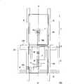
图2A是本发明第一实施例的液晶显示面板的上视示意图,而图2B是沿着图2A中的I2-I2’剖面线所示的剖面示意图。请同时参照图2A及图2B,本实施例的液晶显示面板200包括一薄膜晶体管阵列基板201、一对向基板202以及一液晶层203。薄膜晶体管阵列基板201具有多个像素结构204,而图2A仅示出薄膜晶体管阵列基板201的一个像素结构204及其对向基板202。FIG. 2A is a schematic top view of a liquid crystal display panel according to the first embodiment of the present invention, and FIG. 2B is a schematic cross-sectional view along the line I2-I2' in FIG. 2A. Please refer to FIG. 2A and FIG. 2B at the same time. The liquid
对向基板202配置于薄膜晶体管阵列基板201上方。液晶层203配置于薄膜晶体管阵列基板201与对向基板202之间。对向基板202具有多个配向凸起物P,其目的是使液晶层203中的液晶分子往配向凸起物P倾倒,以使得每一像素中的液晶分子呈多方向排列,进而得到多个不同的配向象限。另外,配向凸起物P上方更有一黑矩阵(Black matrix)BM,其配置于对向基板202上,其中黑矩阵BM的材质例如是由金属、有机材料、彩色光阻或其上述的组合的单层或多层结构所构成,举例而言,黑矩阵BM可由多个彩色光阻叠加而成。The
由图2B可知,薄膜晶体管阵列基板201包括像素结构204,其包括一第一像素电极205、一第二像素电极206以及一顶栅极(Top Gate)薄膜晶体管207。在本实施例中,像素结构204具有一反射区R与一穿透区T。第一像素电极205为一位于反射区R内的反射像素电极,而第二像素电极206为一位于穿透区T内的穿透像素电极。此外,对向基板202的配向凸起物P则分别位于第一像素电极205以及第二像素电极206上方。It can be seen from FIG. 2B that the thin film
本实施例的半穿透半反射式像素结构在显示影像时,穿透区T内的像素电极206为透明电极,以利于让背光源所发出的光线穿透而达到显示的效果,而反射区R内的像素电极205为金属或其他具有良好反射特性材质的反射电极,以利于反射前光源(front-light)或是外界光源搭配而达到显示的效果。在本实施例中,第一像素电极205为表面具有凸块(bump)的铝电极,而穿透像素电极第二像素电极206为可透光的铟锡氧化物(Indium-tin oxide,ITO)。When the semi-transmissive and semi-reflective pixel structure of this embodiment displays an image, the
值得注意的是,在第一像素电极205与第二像素电极206之间存在一连续的主狭缝(continuous main slit)SS使得两像素电极205、206彼此分离。此外,本实施例所描述的像素电极的材料与数目并非用以限定本发明。举例而言,当穿透区T的面积较大时,可将穿透区T的数量增加为2个或是2个以上。另外,像素结构204可进一步包括一栅绝缘层209、一缓冲层210、一第一介电层211、一第一接触导体M1、一第二接触导体M2、一第二介电层212以及一共用电极COM。It should be noted that there is a continuous main slit SS between the
顶栅极薄膜晶体管207配置于薄膜晶体管阵列基板201与第一像素电极205之间,且顶栅极薄膜晶体管207包括一图案化半导体层208以及一栅极G。其中,图案化半导体层208由第一像素电极205下方延伸至第二像素电极206下方,且同时与第一像素电极205以及第二像素电极206电性连接。在本实施例中,图案化半导体层208的材质为多晶硅、单晶硅、微晶硅或非晶硅。由图2B可知,缓冲层210是配置于基板201与图案化半导体层208之间。The top gate
栅绝缘层209配置于基板201上以覆盖图案化半导体层208,其中栅极G配置于栅绝缘层209上。栅绝缘层209与第一介电层211具有一第一接触窗W1以及一第二接触窗W2。第一接触导体M1配置于第一介电层211上,且第一接触导体M1通过第一接触窗W1与图案化半导体层208电性连接。第二接触导体M2配置于第一介电层211上,且第二接触导体M2通过第二接触窗W2与图案化半导体层208电性连接。第二介电层212配置于第一介电层211上,其中第二介电层211具有一第三接触窗W3以及一第四接触窗W4以分别暴露第一接触导体M1以及第二接触导体M2,而第一像素电极205通过第三接触窗W3与第一接触导体M1电性连接,且第二像素电极206通过第四接触窗W4与第二接触导体M2电性连接。The
从图2B可知,第二接触窗W2、第四接触窗W4以及第二接触导体M2的位置与对向基板202的配向凸起物P的位置相对应,如此,配向凸起物P上方的黑矩阵BM可有效地遮蔽第四接触窗W4的漏光,而第二接触导体M2可有效地遮蔽配向凸起物P的漏光。在一些实施例中,依据不同的面板工艺,第二接触窗W2可与第四接触窗W4对准或是稍有错位,同样地,第一接触窗W1亦可与第三接触窗W3对准或稍有错位。在本实施例中,共用电极COM配置于栅绝缘层209上且与图案化半导体层208重叠。详言之,共用电极COM与图案化半导体层208的一部份重叠,且两者之间存在有栅绝缘层209,以形成一储存电容Cst。It can be seen from FIG. 2B that the positions of the second contact window W2, the fourth contact window W4, and the second contact conductor M2 correspond to the positions of the alignment protrusions P on the
请同时参照图2A及图2B,依据上述像素结构204各层之间的配置关系,底下将针对影像信号的传递路径做详细的描述。首先,当经扫描线GL传递一导通信号给栅极G使得顶栅极薄膜晶体管207处于导通状态(ON)时,影像信号由数据线DL传递至第一介电层211上接触窗W的位置,再通过一位于接触窗W位置的接触导体(未示出)与图案化半导体层208电性连接并将信号由数据线DL导入图案化半导体层208。接着,影像信号通过顶栅极薄膜晶体管207后,由图案化半导体层208分别将信号传递至第一介电层211上的第二接触窗W2及第一接触窗W1的位置,再将信号分别导入第二接触导体M2与第一接触导体M1。最后,由于第一像素电极205通过第三接触窗W3与第一接触导体M1电性连接,且第二像素电极206通过第四接触窗W4与第二接触导体M2电性连接,因此通过图案化半导体层208可以将信号成功由数据线DL传递至第一像素电极205与第二像素电极206。在本实施例中,图案化半导体层208将数据线DL的信号,通过多个接触窗W1~W4与接触导体M1、M2直接同时导通到穿透区T与反射区R的电极206、205中,而不是利用公知的连接部105将第一像素电极205的电位导至第二像素电极206。Please refer to FIG. 2A and FIG. 2B at the same time, according to the configuration relationship among the layers of the above-mentioned
由图2A可知,图案化半导体层208实质上呈L形,且其具有多个导电掺杂区208a、208b、208c以及两个连接于导电掺杂区之间的通道区208’、208”,而其中一个导电掺杂区208c由第一像素电极205下方延伸至第二像素电极206下方,且同时与第一像素电极205以及第二像素电极206电性连接。此外,栅极G例如为一具有分支的导线,而此分支导线同时覆盖于上述通道区208’、208”上方,以形成多个顶栅极薄膜晶体管207。It can be seen from FIG. 2A that the patterned
图2C为部份第一接触导体与图案化半导体层在第一接触窗附近的放大示意图。请参照图2C,第一接触导体M1配置于第一介电层211上,并通过第一接触窗W1与图案化半导体层208电性连接。同时与第一像素电极205以及第二像素电极206电性连接的导电掺杂区208c包括一第一型掺杂区D1以及一第二型掺杂区D2。第二型掺杂区D2与第一型掺杂区D1连接,其中第一像素电极205同时与第一型掺杂区D1以及第二型掺杂区D2电性连接,而第二像素电极206仅与第二型掺杂区D2电性连接。2C is an enlarged schematic view of part of the first contact conductor and the patterned semiconductor layer near the first contact window. Referring to FIG. 2C , the first contact conductor M1 is disposed on the
举例而言,储存电容Cst的导电掺杂区208c同时具有N型与P型掺杂,此两种掺杂的分界位在第一接触窗W1正下方。由于第二型掺杂区D2与第一型掺杂区D1连接的接面为一二极管接面J(p-n junction),在接面处会形成一空乏区L(depletion region),不利于电流导通。因此本实施例利用第一接触导体M1通过第一接触窗W1与导电掺杂区208c电性连接,提供电流另一导通路径,使得图案化半导体层208将第一像素电极205的电位导至第二像素电极206时,可以不受二极管接面J的空乏区L影响。For example, the conductive
由于本实施例采用图案化半导体层208直接将影像数据导至第一像素电极205以及第二像素电极206,使得第一像素电极105与第二像素电极106之间不需通过连接部105直接连接,可有效地避免电场在连接部105附近发生严重的扭曲,有助于改善指压色不均(finger press mura)的现象。Since this embodiment uses the patterned
第二实施例second embodiment
在以下的实施例与附图中,相同或相似的标号代表相同或相似的元件,以简化说明。In the following embodiments and drawings, the same or similar reference numerals represent the same or similar components to simplify description.
图3A是本发明第二实施例的液晶显示面板的上视示意图,而图3B是沿着图3A中的I3-I3’剖面线所示的剖面示意图。请同时参照图3A及图3B,本实施例的液晶显示面板200b与第一实施例的液晶显示面板200相似,二者主要差异之处在于:在液晶显示面板200b中,第一像素电极205上方具有一配向图案(alignment patterning)SCF。配向图案SCF配置于对向基板202上,且其下方具有一配向凸起物P。一般而言,多象限垂直配向液晶显示面板通过配向图案SCF搭配多个配向凸起物P,以使得每一像素中的液晶分子呈多方向排列,进而得到多个不同的配向象限,达成广视角的要求。FIG. 3A is a schematic top view of a liquid crystal display panel according to a second embodiment of the present invention, and FIG. 3B is a schematic cross-sectional view along the line I3-I3' in FIG. 3A. Please refer to FIG. 3A and FIG. 3B at the same time. The liquid
因此,通过在第一实施例的第一像素电极205上方配置一配位图案SCF,可改变反射区R中液晶层203的间隙(cell-gap),使本实施例的半穿透半反射式像素结构204为双间隙(Dual cell-gap)结构。也就是说,穿透区T与反射区R分别具有不同厚度的液晶层203。举例而言,穿透区T的液晶层间隙为D1,而在第一实施例的穿透区R的液晶层间隙亦为D1,但在配置配位图案SCF后,本实施例的反射区R的液晶层间隙则变为D2,且D2相当于D1的二分之一。Therefore, by disposing a coordination pattern SCF above the
本实施例的双间隙结构可使穿透区T与反射区R具有相同的相位延迟(phase retardation),以进一步提升半穿透半反射式液晶显示面板200b的显示品质。The double-gap structure of this embodiment can make the transmissive region T and the reflective region R have the same phase retardation, so as to further improve the display quality of the transflective liquid
第三实施例third embodiment
图4A是本发明第三实施例的液晶显示面板的上视示意图,而图4B是沿着图4A中的I4-I4’剖面线所示的剖面示意图。请同时参照图4A及图4B,本实施例的液晶显示面板200c与第二实施例的液晶显示面板200b相似,二者主要差异之处在于:在液晶显示面板200c的反射区R中,垫高层213是配置于部份第二介电层212上。4A is a schematic top view of a liquid crystal display panel according to a third embodiment of the present invention, and FIG. 4B is a schematic cross-sectional view along the line I4-I4' in FIG. 4A. Please refer to FIG. 4A and FIG. 4B at the same time. The liquid
更详细的来说,本实施例的像素结构204进一步包括一栅绝缘层209、一第一介电层211、一第一接触导体M1、一第二接触导体M2、一第二介电层212以及一垫高层213。栅绝缘层209覆盖图案化半导体层208,其中栅极G配置于栅绝缘层209上,且栅绝缘层209与第一介电层211具有一第一接触窗W1以及一第二接触窗W2。第一接触导体M1配置于第一介电层211上,并通过第一接触窗W1与图案化半导体层208电性连接。第二接触导体M2配置于第一介电层211上,并通过第二接触窗W2与图案化半导体层208电性连接。第二介电层212配置于第一介电层211上。垫高层213配置于部分的第二介电层212上,其中垫高层213与第二介电层212具有一第三接触窗W3以暴露第一接触导体M1,而第二介电层212c具有一第四接触窗W4以暴露第二接触导体M2,第一像素电极205通过第三接触窗W3与第一接触导体M1电性连接,且第二像素电极206通过第四接触窗W4与第二接触导体M2电性连接。In more detail, the
垫高层213功用类似于第二实施例的配向图案SCF,可将本实施例的半穿透半反射式像素结构204c变为双间隙结构。也就是说,本实施例的穿透区T的液晶层间隙为D1,反射区R的液晶层间隙则变为D2’,且D2’相当于D1的二分之一,以提升半穿透半反射式液晶显示面板200c的显示品质。The function of the
第四实施例Fourth embodiment
图5A是本发明第四实施例的液晶显示面板的上视示意图,而图5B是沿着图5A中的I5-I5’剖面线所示的剖面示意图。请同时参照图5A及图5B,本实施例的液晶显示面板200d与第一实施例的液晶显示面板200相似,二者其中的一差异之处在于:液晶显示面板200d的第一像素电极205与第二像素电极206皆为穿透像素电极。也就是说,液晶显示面板200d的像素结构204具有两个穿透区T1、T2。值得注意的是,在其他实施例中,液晶显示面板的第一像素电极205与第二像素电极206亦可皆为反射像素电极。FIG. 5A is a schematic top view of a liquid crystal display panel according to a fourth embodiment of the present invention, and FIG. 5B is a schematic cross-sectional view along the line I5-I5' in FIG. 5A. Please refer to FIG. 5A and FIG. 5B at the same time. The liquid crystal display panel 200d of this embodiment is similar to the liquid
由图5B可知,液晶显示面板200d与第一实施例的液晶显示面板200另一不同点在于:本实施例的共用电极COM配置于栅绝缘层209上且于第一接触窗W1的位置具有一开口214,其中共用电极COM与部分的导电掺杂区208重叠,以形成储存电容Cst。It can be seen from FIG. 5B that another difference between the liquid crystal display panel 200d and the liquid
第五实施例fifth embodiment
图6A是本发明第五实施例的液晶显示面板中的一像素结构及其对向基板的上视示意图,图6B是沿着图6A中的I6-I6’剖面线所示的剖面示意图。请同时参照图6A及图6B,本实施例的液晶显示面板200e与第四实施例的液晶显示面板200d相似,但二者主要差异之处在于:本实施例的像素结构204的共用电极COM呈十字形。也就是说,共用电极COM除了分布在第一穿透区T1与第二穿透区T2之间的主狭缝SS下方之外,亦分布在第三接触窗W3与第四接触窗W4的连线上,此十字形的共用电极COM可增加储存电容Cst的大小。6A is a schematic top view of a pixel structure and its opposite substrate in a liquid crystal display panel according to a fifth embodiment of the present invention, and FIG. 6B is a schematic cross-sectional view along line I6-I6' in FIG. 6A. Please refer to FIG. 6A and FIG. 6B at the same time. The liquid
综上所述,本发明的液晶显示面板至少具有下列优点:In summary, the liquid crystal display panel of the present invention has at least the following advantages:
1.由于本发明采用图案化半导体层直接将影像数据导至第一像素电极以及第二像素电极,使得第一像素电极与第二像素电极之间不需通过连接部直接连接,因此液晶分子不会受到公知连接部扭曲电场的影响,有助于液晶显示面板在遭受外力按压之后,较不容易有色不均(Mura)的问题。1. Since the present invention uses a patterned semiconductor layer to directly guide the image data to the first pixel electrode and the second pixel electrode, so that the first pixel electrode and the second pixel electrode do not need to be directly connected through the connecting part, so the liquid crystal molecules do not need to be connected directly. It will be affected by the twisted electric field of the known connection part, which helps the liquid crystal display panel to be less prone to the problem of color unevenness (Mura) after being pressed by an external force.
2.在本发明的部分实施例中,设计者可视需求而将像素结构设计为双间隙结构,以提升半穿透半反射式液晶显示面板的显示品质。2. In some embodiments of the present invention, the designer can design the pixel structure as a double-gap structure according to requirements, so as to improve the display quality of the transflective liquid crystal display panel.
3.在本发明的部分实施例中,利用十字形共用电极增加储存电容Cst的大小,以提升薄膜晶体管保持电位的能力,并可减少因电容耦合效应而产生的电压变化量,进一步改善面板的显示品质。3. In some embodiments of the present invention, the cross-shaped common electrode is used to increase the size of the storage capacitor Cst to improve the ability of the thin film transistor to maintain the potential, and can reduce the voltage variation caused by the capacitive coupling effect, further improving the performance of the panel. display quality.
当然,本发明还可有其它多种实施例,在不背离本发明精神及其实质的情况下,熟悉本领域的技术人员当可根据本发明作出各种相应的改变和变形,但这些相应的改变和变形都应属于本发明所附的权利要求的保护范围。Certainly, the present invention also can have other multiple embodiments, without departing from the spirit and essence of the present invention, those skilled in the art can make various corresponding changes and deformations according to the present invention, but these corresponding Changes and deformations should belong to the scope of protection of the appended claims of the present invention.
Claims (14)
Translated fromChinesePriority Applications (1)
| Application Number | Priority Date | Filing Date | Title |
|---|---|---|---|
| CN2008101467858ACN101344697B (en) | 2008-08-29 | 2008-08-29 | Pixel structure and liquid crystal display panel |
Applications Claiming Priority (1)
| Application Number | Priority Date | Filing Date | Title |
|---|---|---|---|
| CN2008101467858ACN101344697B (en) | 2008-08-29 | 2008-08-29 | Pixel structure and liquid crystal display panel |
Publications (2)
| Publication Number | Publication Date |
|---|---|
| CN101344697Atrue CN101344697A (en) | 2009-01-14 |
| CN101344697B CN101344697B (en) | 2010-04-21 |
Family
ID=40246719
Family Applications (1)
| Application Number | Title | Priority Date | Filing Date |
|---|---|---|---|
| CN2008101467858AActiveCN101344697B (en) | 2008-08-29 | 2008-08-29 | Pixel structure and liquid crystal display panel |
Country Status (1)
| Country | Link |
|---|---|
| CN (1) | CN101344697B (en) |
Cited By (5)
| Publication number | Priority date | Publication date | Assignee | Title |
|---|---|---|---|---|
| CN105116650A (en)* | 2015-09-01 | 2015-12-02 | 深圳市华星光电技术有限公司 | Liquid crystal display panel |
| CN105404061A (en)* | 2014-09-09 | 2016-03-16 | 株式会社日本显示器 | Liquid crystal display device and display device |
| WO2016165264A1 (en)* | 2015-04-13 | 2016-10-20 | 京东方科技集团股份有限公司 | Pixel unit and preparation method therefor, array substrate and display device |
| JP2017227856A (en)* | 2015-08-07 | 2017-12-28 | 株式会社半導体エネルギー研究所 | Display panel, information processing apparatus, and display panel driving method |
| JP2018022038A (en)* | 2016-08-03 | 2018-02-08 | 株式会社半導体エネルギー研究所 | Display device and electronic apparatus |
Family Cites Families (2)
| Publication number | Priority date | Publication date | Assignee | Title |
|---|---|---|---|---|
| CN1288480C (en)* | 2002-11-25 | 2006-12-06 | 统宝光电股份有限公司 | Transflective LCD |
| KR100617290B1 (en)* | 2003-12-30 | 2006-08-30 | 엘지.필립스 엘시디 주식회사 | Reflective Transmissive Liquid Crystal Display Array Substrate and Manufacturing Method Thereof |
- 2008
- 2008-08-29CNCN2008101467858Apatent/CN101344697B/enactiveActive
Cited By (9)
| Publication number | Priority date | Publication date | Assignee | Title |
|---|---|---|---|---|
| CN105404061A (en)* | 2014-09-09 | 2016-03-16 | 株式会社日本显示器 | Liquid crystal display device and display device |
| CN105404061B (en)* | 2014-09-09 | 2018-08-03 | 株式会社日本显示器 | Liquid crystal display device and display device |
| US10353259B2 (en) | 2014-09-09 | 2019-07-16 | Japan Display Inc. | Liquid crystal display device and display device |
| WO2016165264A1 (en)* | 2015-04-13 | 2016-10-20 | 京东方科技集团股份有限公司 | Pixel unit and preparation method therefor, array substrate and display device |
| US10332917B2 (en) | 2015-04-13 | 2019-06-25 | Boe Technology Croup Co., Ltd. | Pixel unit and method for producing the same, array substrate and display apparatus |
| JP2017227856A (en)* | 2015-08-07 | 2017-12-28 | 株式会社半導体エネルギー研究所 | Display panel, information processing apparatus, and display panel driving method |
| CN105116650A (en)* | 2015-09-01 | 2015-12-02 | 深圳市华星光电技术有限公司 | Liquid crystal display panel |
| CN105116650B (en)* | 2015-09-01 | 2019-01-01 | 深圳市华星光电技术有限公司 | Liquid crystal display panel |
| JP2018022038A (en)* | 2016-08-03 | 2018-02-08 | 株式会社半導体エネルギー研究所 | Display device and electronic apparatus |
Also Published As
| Publication number | Publication date |
|---|---|
| CN101344697B (en) | 2010-04-21 |
Similar Documents
| Publication | Publication Date | Title |
|---|---|---|
| JP5165169B2 (en) | Liquid crystal display | |
| US10288955B2 (en) | Liquid crystal display device | |
| US7636144B2 (en) | Liquid crystal display device and method of manufacturing the same | |
| US11467455B2 (en) | Display device | |
| JP2014109777A (en) | Liquid crystal display device | |
| CN101344697B (en) | Pixel structure and liquid crystal display panel | |
| CN101750827B (en) | Active element array substrate | |
| CN105470266A (en) | FFS (fringe field switching) type array substrate and manufacturing method therefor | |
| US10928686B2 (en) | Array substrate, liquid crystal display panel and display device | |
| US9599855B2 (en) | Liquid crystal display | |
| US8085354B2 (en) | Pixel structure with semiconductor of top-gate TFT extended over electrodes and liquid crystal display panel | |
| US8451413B2 (en) | Array substrate for FFS type LCD panel and method for manufacturing the same | |
| US10025137B2 (en) | Liquid crystal display device having transmitting region and reflecting region | |
| CN101126881A (en) | LCD panel and pixels | |
| JP4007338B2 (en) | Liquid crystal display device and electronic device | |
| US20200335531A1 (en) | Thin-film transistor substrate, display panel, and display device | |
| JP2023036194A (en) | Display device | |
| US9134578B2 (en) | Liquid crystal display device | |
| JP4110889B2 (en) | Liquid crystal display | |
| KR20210012194A (en) | Thin film transistor and display device comprising the same | |
| US20110063551A1 (en) | Liquid crystal display device | |
| US8212980B2 (en) | Liquid crystal display and active matrix substrate | |
| US11003031B2 (en) | Display apparatus | |
| TWI435150B (en) | Liquid display panel and manufacturing method thereof | |
| JP2025000212A (en) | Display device and array substrate |
Legal Events
| Date | Code | Title | Description |
|---|---|---|---|
| C06 | Publication | ||
| PB01 | Publication | ||
| C10 | Entry into substantive examination | ||
| SE01 | Entry into force of request for substantive examination | ||
| C14 | Grant of patent or utility model | ||
| GR01 | Patent grant |