CN101339960B - Light-emitting device - Google Patents
Light-emitting deviceDownload PDFInfo
- Publication number
- CN101339960B CN101339960BCN2008101379043ACN200810137904ACN101339960BCN 101339960 BCN101339960 BCN 101339960BCN 2008101379043 ACN2008101379043 ACN 2008101379043ACN 200810137904 ACN200810137904 ACN 200810137904ACN 101339960 BCN101339960 BCN 101339960B
- Authority
- CN
- China
- Prior art keywords
- buffer layer
- semiconductor film
- electrode
- film
- source
- Prior art date
- Legal status (The legal status is an assumption and is not a legal conclusion. Google has not performed a legal analysis and makes no representation as to the accuracy of the status listed.)
- Expired - Fee Related
Links
- 239000004065semiconductorSubstances0.000claimsabstractdescription272
- 239000000872bufferSubstances0.000claimsabstractdescription126
- IJGRMHOSHXDMSA-UHFFFAOYSA-NAtomic nitrogenChemical compoundN#NIJGRMHOSHXDMSA-UHFFFAOYSA-N0.000claimsdescription53
- UFHFLCQGNIYNRP-UHFFFAOYSA-NHydrogenChemical compound[H][H]UFHFLCQGNIYNRP-UHFFFAOYSA-N0.000claimsdescription38
- 239000001257hydrogenSubstances0.000claimsdescription37
- 229910052739hydrogenInorganic materials0.000claimsdescription37
- 229910052757nitrogenInorganic materials0.000claimsdescription26
- 239000011737fluorineSubstances0.000claimsdescription14
- 229910052731fluorineInorganic materials0.000claimsdescription14
- 239000000460chlorineSubstances0.000claimsdescription11
- ZCYVEMRRCGMTRW-UHFFFAOYSA-N7553-56-2Chemical compound[I]ZCYVEMRRCGMTRW-UHFFFAOYSA-N0.000claimsdescription9
- 239000011630iodineSubstances0.000claimsdescription9
- 229910052740iodineInorganic materials0.000claimsdescription9
- WKBOTKDWSSQWDR-UHFFFAOYSA-NBromine atomChemical compound[Br]WKBOTKDWSSQWDR-UHFFFAOYSA-N0.000claimsdescription7
- ZAMOUSCENKQFHK-UHFFFAOYSA-NChlorine atomChemical compound[Cl]ZAMOUSCENKQFHK-UHFFFAOYSA-N0.000claimsdescription7
- GDTBXPJZTBHREO-UHFFFAOYSA-NbromineSubstancesBrBrGDTBXPJZTBHREO-UHFFFAOYSA-N0.000claimsdescription7
- 229910052794bromiumInorganic materials0.000claimsdescription7
- 229910052801chlorineInorganic materials0.000claimsdescription7
- PXGOKWXKJXAPGV-UHFFFAOYSA-NFluorineChemical compoundFFPXGOKWXKJXAPGV-UHFFFAOYSA-N0.000claims5
- 239000010408filmSubstances0.000abstractdescription569
- 239000010409thin filmSubstances0.000abstractdescription202
- 230000015572biosynthetic processEffects0.000abstractdescription59
- 238000000034methodMethods0.000abstractdescription34
- 238000004519manufacturing processMethods0.000abstractdescription25
- 239000013081microcrystalSubstances0.000abstract1
- 239000010410layerSubstances0.000description112
- 239000000758substrateSubstances0.000description79
- 108091006146ChannelsProteins0.000description57
- 239000007789gasSubstances0.000description57
- 239000012535impuritySubstances0.000description52
- 238000006243chemical reactionMethods0.000description46
- 229910021417amorphous siliconInorganic materials0.000description36
- XUIMIQQOPSSXEZ-UHFFFAOYSA-NSiliconChemical compound[Si]XUIMIQQOPSSXEZ-UHFFFAOYSA-N0.000description34
- 229910052710siliconInorganic materials0.000description34
- 239000010703siliconSubstances0.000description34
- 238000012545processingMethods0.000description30
- BLRPTPMANUNPDV-UHFFFAOYSA-NSilaneChemical compound[SiH4]BLRPTPMANUNPDV-UHFFFAOYSA-N0.000description28
- 229910021424microcrystalline siliconInorganic materials0.000description27
- XKRFYHLGVUSROY-UHFFFAOYSA-NArgonChemical compound[Ar]XKRFYHLGVUSROY-UHFFFAOYSA-N0.000description24
- 238000005268plasma chemical vapour depositionMethods0.000description24
- 229910052990silicon hydrideInorganic materials0.000description23
- 230000001681protective effectEffects0.000description21
- 230000008569processEffects0.000description17
- 239000013078crystalSubstances0.000description16
- 229910052581Si3N4Inorganic materials0.000description14
- VYPSYNLAJGMNEJ-UHFFFAOYSA-NSilicium dioxideChemical compoundO=[Si]=OVYPSYNLAJGMNEJ-UHFFFAOYSA-N0.000description14
- 238000005530etchingMethods0.000description14
- 229910052734heliumInorganic materials0.000description14
- 239000001307heliumSubstances0.000description14
- SWQJXJOGLNCZEY-UHFFFAOYSA-Nhelium atomChemical compound[He]SWQJXJOGLNCZEY-UHFFFAOYSA-N0.000description14
- 239000000463materialSubstances0.000description14
- HQVNEWCFYHHQES-UHFFFAOYSA-Nsilicon nitrideChemical compoundN12[Si]34N5[Si]62N3[Si]51N64HQVNEWCFYHHQES-UHFFFAOYSA-N0.000description14
- QVGXLLKOCUKJST-UHFFFAOYSA-Natomic oxygenChemical compound[O]QVGXLLKOCUKJST-UHFFFAOYSA-N0.000description13
- 229910052760oxygenInorganic materials0.000description13
- 239000001301oxygenSubstances0.000description13
- 229910052814silicon oxideInorganic materials0.000description13
- 229910052786argonInorganic materials0.000description12
- 229910052743kryptonInorganic materials0.000description11
- DNNSSWSSYDEUBZ-UHFFFAOYSA-Nkrypton atomChemical compound[Kr]DNNSSWSSYDEUBZ-UHFFFAOYSA-N0.000description11
- 238000010586diagramMethods0.000description10
- QGZKDVFQNNGYKY-UHFFFAOYSA-NAmmoniaChemical compoundNQGZKDVFQNNGYKY-UHFFFAOYSA-N0.000description8
- ZOKXTWBITQBERF-UHFFFAOYSA-NMolybdenumChemical compound[Mo]ZOKXTWBITQBERF-UHFFFAOYSA-N0.000description8
- 229910052782aluminiumInorganic materials0.000description8
- 239000004020conductorSubstances0.000description8
- 230000006870functionEffects0.000description8
- 229910052750molybdenumInorganic materials0.000description8
- 239000011733molybdenumSubstances0.000description8
- 230000003647oxidationEffects0.000description8
- 238000007254oxidation reactionMethods0.000description8
- 229910052736halogenInorganic materials0.000description7
- 150000002367halogensChemical class0.000description7
- 238000003475laminationMethods0.000description7
- 229910052754neonInorganic materials0.000description7
- GKAOGPIIYCISHV-UHFFFAOYSA-Nneon atomChemical compound[Ne]GKAOGPIIYCISHV-UHFFFAOYSA-N0.000description7
- 238000005192partitionMethods0.000description7
- ZOXJGFHDIHLPTG-UHFFFAOYSA-NBoronChemical compound[B]ZOXJGFHDIHLPTG-UHFFFAOYSA-N0.000description6
- YCKRFDGAMUMZLT-UHFFFAOYSA-NFluorine atomChemical compound[F]YCKRFDGAMUMZLT-UHFFFAOYSA-N0.000description6
- GQPLMRYTRLFLPF-UHFFFAOYSA-NNitrous OxideChemical compound[O-][N+]#NGQPLMRYTRLFLPF-UHFFFAOYSA-N0.000description6
- RTAQQCXQSZGOHL-UHFFFAOYSA-NTitaniumChemical compound[Ti]RTAQQCXQSZGOHL-UHFFFAOYSA-N0.000description6
- XAGFODPZIPBFFR-UHFFFAOYSA-NaluminiumChemical compound[Al]XAGFODPZIPBFFR-UHFFFAOYSA-N0.000description6
- 229910052796boronInorganic materials0.000description6
- 239000000969carrierSubstances0.000description6
- 238000009826distributionMethods0.000description6
- 150000002431hydrogenChemical class0.000description6
- 229920005989resinPolymers0.000description6
- 239000011347resinSubstances0.000description6
- 238000004088simulationMethods0.000description6
- 239000002356single layerSubstances0.000description6
- 229910052719titaniumInorganic materials0.000description6
- 239000010936titaniumSubstances0.000description6
- 125000004429atomChemical group0.000description5
- 230000005540biological transmissionEffects0.000description5
- 229920001940conductive polymerPolymers0.000description5
- 238000002425crystallisationMethods0.000description5
- 230000008025crystallizationEffects0.000description5
- 238000001312dry etchingMethods0.000description5
- 239000011521glassSubstances0.000description5
- AMGQUBHHOARCQH-UHFFFAOYSA-Nindium;oxotinChemical compound[In].[Sn]=OAMGQUBHHOARCQH-UHFFFAOYSA-N0.000description5
- 229910052751metalInorganic materials0.000description5
- 239000002184metalSubstances0.000description5
- 239000000203mixtureSubstances0.000description5
- 229910000077silaneInorganic materials0.000description5
- 238000004544sputter depositionMethods0.000description5
- OAICVXFJPJFONN-UHFFFAOYSA-NPhosphorusChemical compound[P]OAICVXFJPJFONN-UHFFFAOYSA-N0.000description4
- 238000001069Raman spectroscopyMethods0.000description4
- GWEVSGVZZGPLCZ-UHFFFAOYSA-NTitan oxideChemical compoundO=[Ti]=OGWEVSGVZZGPLCZ-UHFFFAOYSA-N0.000description4
- 229910021529ammoniaInorganic materials0.000description4
- 230000015556catabolic processEffects0.000description4
- 229910021419crystalline siliconInorganic materials0.000description4
- 238000006731degradation reactionMethods0.000description4
- 238000005401electroluminescenceMethods0.000description4
- 229910003437indium oxideInorganic materials0.000description4
- PJXISJQVUVHSOJ-UHFFFAOYSA-Nindium(iii) oxideChemical compound[O-2].[O-2].[O-2].[In+3].[In+3]PJXISJQVUVHSOJ-UHFFFAOYSA-N0.000description4
- 238000011068loading methodMethods0.000description4
- 150000004767nitridesChemical class0.000description4
- QGLKJKCYBOYXKC-UHFFFAOYSA-NnonaoxidotritungstenChemical compoundO=[W]1(=O)O[W](=O)(=O)O[W](=O)(=O)O1QGLKJKCYBOYXKC-UHFFFAOYSA-N0.000description4
- 239000002245particleSubstances0.000description4
- 229910052698phosphorusInorganic materials0.000description4
- 239000011574phosphorusSubstances0.000description4
- 238000009832plasma treatmentMethods0.000description4
- 239000003566sealing materialSubstances0.000description4
- 150000003376siliconChemical class0.000description4
- 230000005236sound signalEffects0.000description4
- OGIDPMRJRNCKJF-UHFFFAOYSA-Ntitanium oxideInorganic materials[Ti]=OOGIDPMRJRNCKJF-UHFFFAOYSA-N0.000description4
- WFKWXMTUELFFGS-UHFFFAOYSA-NtungstenChemical compound[W]WFKWXMTUELFFGS-UHFFFAOYSA-N0.000description4
- 229910052721tungstenInorganic materials0.000description4
- 239000010937tungstenSubstances0.000description4
- 229910001930tungsten oxideInorganic materials0.000description4
- 229910052724xenonInorganic materials0.000description4
- FHNFHKCVQCLJFQ-UHFFFAOYSA-Nxenon atomChemical compound[Xe]FHNFHKCVQCLJFQ-UHFFFAOYSA-N0.000description4
- YVTHLONGBIQYBO-UHFFFAOYSA-Nzinc indium(3+) oxygen(2-)Chemical compound[O--].[Zn++].[In+3]YVTHLONGBIQYBO-UHFFFAOYSA-N0.000description4
- 229910000838Al alloyInorganic materials0.000description3
- VYZAMTAEIAYCRO-UHFFFAOYSA-NChromiumChemical compound[Cr]VYZAMTAEIAYCRO-UHFFFAOYSA-N0.000description3
- NIXOWILDQLNWCW-UHFFFAOYSA-Nacrylic acid groupChemical groupC(C=C)(=O)ONIXOWILDQLNWCW-UHFFFAOYSA-N0.000description3
- 238000004140cleaningMethods0.000description3
- 238000000151depositionMethods0.000description3
- 238000011161developmentMethods0.000description3
- 238000001678elastic recoil detection analysisMethods0.000description3
- 230000005685electric field effectEffects0.000description3
- 230000005669field effectEffects0.000description3
- 230000007246mechanismEffects0.000description3
- 229910021421monocrystalline siliconInorganic materials0.000description3
- 229960001730nitrous oxideDrugs0.000description3
- 150000002894organic compoundsChemical class0.000description3
- 239000000126substanceSubstances0.000description3
- 229910052715tantalumInorganic materials0.000description3
- GUVRBAGPIYLISA-UHFFFAOYSA-Ntantalum atomChemical compound[Ta]GUVRBAGPIYLISA-UHFFFAOYSA-N0.000description3
- 238000001039wet etchingMethods0.000description3
- 229910017073AlLiInorganic materials0.000description2
- OKTJSMMVPCPJKN-UHFFFAOYSA-NCarbonChemical compound[C]OKTJSMMVPCPJKN-UHFFFAOYSA-N0.000description2
- CURLTUGMZLYLDI-UHFFFAOYSA-NCarbon dioxideChemical compoundO=C=OCURLTUGMZLYLDI-UHFFFAOYSA-N0.000description2
- MYMOFIZGZYHOMD-UHFFFAOYSA-NDioxygenChemical compoundO=OMYMOFIZGZYHOMD-UHFFFAOYSA-N0.000description2
- 206010052128GlareDiseases0.000description2
- VEXZGXHMUGYJMC-UHFFFAOYSA-NHydrochloric acidChemical compoundClVEXZGXHMUGYJMC-UHFFFAOYSA-N0.000description2
- 239000004642PolyimideSubstances0.000description2
- 238000001237Raman spectrumMethods0.000description2
- 229910003902SiCl 4Inorganic materials0.000description2
- WGLPBDUCMAPZCE-UHFFFAOYSA-NTrioxochromiumChemical compoundO=[Cr](=O)=OWGLPBDUCMAPZCE-UHFFFAOYSA-N0.000description2
- 238000004380ashingMethods0.000description2
- DQXBYHZEEUGOBF-UHFFFAOYSA-Nbut-3-enoic acid;etheneChemical compoundC=C.OC(=O)CC=CDQXBYHZEEUGOBF-UHFFFAOYSA-N0.000description2
- 229910052799carbonInorganic materials0.000description2
- SLLGVCUQYRMELA-UHFFFAOYSA-NchlorosiliconChemical compoundCl[Si]SLLGVCUQYRMELA-UHFFFAOYSA-N0.000description2
- 229910052804chromiumInorganic materials0.000description2
- 239000011651chromiumSubstances0.000description2
- 229910000423chromium oxideInorganic materials0.000description2
- 238000004891communicationMethods0.000description2
- 238000011109contaminationMethods0.000description2
- 230000007423decreaseEffects0.000description2
- 238000013461designMethods0.000description2
- 238000001514detection methodMethods0.000description2
- 229910001882dioxygenInorganic materials0.000description2
- -1etc.Substances0.000description2
- 239000005038ethylene vinyl acetateSubstances0.000description2
- 230000005281excited stateEffects0.000description2
- 239000000945fillerSubstances0.000description2
- 238000002347injectionMethods0.000description2
- 239000007924injectionSubstances0.000description2
- 230000001678irradiating effectEffects0.000description2
- 239000007769metal materialSubstances0.000description2
- 235000013842nitrous oxideNutrition0.000description2
- AHLBNYSZXLDEJQ-FWEHEUNISA-NorlistatChemical compoundCCCCCCCCCCC[C@H](OC(=O)[C@H](CC(C)C)NC=O)C[C@@H]1OC(=O)[C@H]1CCCCCCAHLBNYSZXLDEJQ-FWEHEUNISA-N0.000description2
- 230000000737periodic effectEffects0.000description2
- 229920001200poly(ethylene-vinyl acetate)Polymers0.000description2
- 229920002037poly(vinyl butyral) polymerPolymers0.000description2
- 229920001721polyimidePolymers0.000description2
- 229920000915polyvinyl chloridePolymers0.000description2
- 239000004800polyvinyl chlorideSubstances0.000description2
- 239000002994raw materialSubstances0.000description2
- 230000006798recombinationEffects0.000description2
- 238000005215recombinationMethods0.000description2
- 230000009467reductionEffects0.000description2
- 238000005001rutherford backscattering spectroscopyMethods0.000description2
- UGFAIRIUMAVXCW-UHFFFAOYSA-NCarbon monoxideChemical compound[O+]#[C-]UGFAIRIUMAVXCW-UHFFFAOYSA-N0.000description1
- RYGMFSIKBFXOCR-UHFFFAOYSA-NCopperChemical compound[Cu]RYGMFSIKBFXOCR-UHFFFAOYSA-N0.000description1
- 229910019974CrSiInorganic materials0.000description1
- 229910016006MoSiInorganic materials0.000description1
- 102000004129N-Type Calcium ChannelsHuman genes0.000description1
- 108090000699N-Type Calcium ChannelsProteins0.000description1
- 229910052779NeodymiumInorganic materials0.000description1
- 238000006124Pilkington processMethods0.000description1
- 239000004952PolyamideSubstances0.000description1
- NRTOMJZYCJJWKI-UHFFFAOYSA-NTitanium nitrideChemical compound[Ti]#NNRTOMJZYCJJWKI-UHFFFAOYSA-N0.000description1
- 239000000956alloySubstances0.000description1
- 239000005407aluminoborosilicate glassSubstances0.000description1
- 239000005354aluminosilicate glassSubstances0.000description1
- 230000003321amplificationEffects0.000description1
- 239000010405anode materialSubstances0.000description1
- 229910052788bariumInorganic materials0.000description1
- DSAJWYNOEDNPEQ-UHFFFAOYSA-Nbarium atomChemical compound[Ba]DSAJWYNOEDNPEQ-UHFFFAOYSA-N0.000description1
- 230000004888barrier functionEffects0.000description1
- 239000011230binding agentSubstances0.000description1
- 239000005388borosilicate glassSubstances0.000description1
- 229910002092carbon dioxideInorganic materials0.000description1
- 239000001569carbon dioxideSubstances0.000description1
- 239000000919ceramicSubstances0.000description1
- 239000011248coating agentSubstances0.000description1
- 238000000576coating methodMethods0.000description1
- 150000001875compoundsChemical class0.000description1
- 229920001577copolymerPolymers0.000description1
- 229910052802copperInorganic materials0.000description1
- 239000010949copperSubstances0.000description1
- 238000009792diffusion processMethods0.000description1
- 238000010790dilutionMethods0.000description1
- 239000012895dilutionSubstances0.000description1
- 229910001873dinitrogenInorganic materials0.000description1
- KPUWHANPEXNPJT-UHFFFAOYSA-NdisiloxaneChemical class[SiH3]O[SiH3]KPUWHANPEXNPJT-UHFFFAOYSA-N0.000description1
- 239000006185dispersionSubstances0.000description1
- 230000005684electric fieldEffects0.000description1
- 230000005611electricityEffects0.000description1
- 230000005274electronic transitionsEffects0.000description1
- 239000003344environmental pollutantSubstances0.000description1
- 239000003822epoxy resinSubstances0.000description1
- 230000005284excitationEffects0.000description1
- 239000000284extractSubstances0.000description1
- 238000011049fillingMethods0.000description1
- 230000004313glareEffects0.000description1
- 230000005283ground stateEffects0.000description1
- LNEPOXFFQSENCJ-UHFFFAOYSA-NhaloperidolChemical compoundC1CC(O)(C=2C=CC(Cl)=CC=2)CCN1CCCC(=O)C1=CC=C(F)C=C1LNEPOXFFQSENCJ-UHFFFAOYSA-N0.000description1
- 238000010438heat treatmentMethods0.000description1
- 230000005525hole transportEffects0.000description1
- 239000011261inert gasSubstances0.000description1
- 150000002484inorganic compoundsChemical class0.000description1
- 229910010272inorganic materialInorganic materials0.000description1
- 238000007689inspectionMethods0.000description1
- 230000002452interceptive effectEffects0.000description1
- 150000002500ionsChemical class0.000description1
- 238000005499laser crystallizationMethods0.000description1
- 238000012423maintenanceMethods0.000description1
- 239000011159matrix materialSubstances0.000description1
- 230000008018meltingEffects0.000description1
- 238000002844meltingMethods0.000description1
- 229910021645metal ionInorganic materials0.000description1
- QLOAVXSYZAJECW-UHFFFAOYSA-Nmethane;molecular fluorineChemical compoundC.FFQLOAVXSYZAJECW-UHFFFAOYSA-N0.000description1
- QEFYFXOXNSNQGX-UHFFFAOYSA-Nneodymium atomChemical compound[Nd]QEFYFXOXNSNQGX-UHFFFAOYSA-N0.000description1
- GVGCUCJTUSOZKP-UHFFFAOYSA-Nnitrogen trifluorideChemical compoundFN(F)FGVGCUCJTUSOZKP-UHFFFAOYSA-N0.000description1
- 239000001272nitrous oxideSubstances0.000description1
- 229910052756noble gasInorganic materials0.000description1
- 238000003199nucleic acid amplification methodMethods0.000description1
- 230000003287optical effectEffects0.000description1
- 239000012788optical filmSubstances0.000description1
- 230000003071parasitic effectEffects0.000description1
- 238000000206photolithographyMethods0.000description1
- 229920002120photoresistant polymerPolymers0.000description1
- 238000002294plasma sputter depositionMethods0.000description1
- 229920003023plasticPolymers0.000description1
- 239000004033plasticSubstances0.000description1
- 239000002985plastic filmSubstances0.000description1
- 231100000719pollutantToxicity0.000description1
- 229920002647polyamidePolymers0.000description1
- 229920000767polyanilinePolymers0.000description1
- 229920000647polyepoxidePolymers0.000description1
- 229920006267polyester filmPolymers0.000description1
- 229920000128polypyrrolePolymers0.000description1
- 229920001296polysiloxanePolymers0.000description1
- 229920000123polythiophenePolymers0.000description1
- 238000003672processing methodMethods0.000description1
- 239000010453quartzSubstances0.000description1
- 239000000376reactantSubstances0.000description1
- 230000004043responsivenessEffects0.000description1
- 230000000630rising effectEffects0.000description1
- 229910052706scandiumInorganic materials0.000description1
- SIXSYDAISGFNSX-UHFFFAOYSA-Nscandium atomChemical compound[Sc]SIXSYDAISGFNSX-UHFFFAOYSA-N0.000description1
- 238000000926separation methodMethods0.000description1
- 229920002050silicone resinPolymers0.000description1
- 238000009751slip formingMethods0.000description1
- 238000001228spectrumMethods0.000description1
- 230000002269spontaneous effectEffects0.000description1
- 229910001256stainless steel alloyInorganic materials0.000description1
- 230000003068static effectEffects0.000description1
- 238000006557surface reactionMethods0.000description1
- 229920001187thermosetting polymerPolymers0.000description1
- XOLBLPGZBRYERU-UHFFFAOYSA-Ntin dioxideChemical compoundO=[Sn]=OXOLBLPGZBRYERU-UHFFFAOYSA-N0.000description1
- 229910001887tin oxideInorganic materials0.000description1
- 238000012546transferMethods0.000description1
- 238000002834transmittanceMethods0.000description1
- 238000001771vacuum depositionMethods0.000description1
- 238000007738vacuum evaporationMethods0.000description1
- XLYOFNOQVPJJNP-UHFFFAOYSA-NwaterChemical compoundOXLYOFNOQVPJJNP-UHFFFAOYSA-N0.000description1
Images


Classifications
- H—ELECTRICITY
- H10—SEMICONDUCTOR DEVICES; ELECTRIC SOLID-STATE DEVICES NOT OTHERWISE PROVIDED FOR
- H10D—INORGANIC ELECTRIC SEMICONDUCTOR DEVICES
- H10D30/00—Field-effect transistors [FET]
- H10D30/60—Insulated-gate field-effect transistors [IGFET]
- H10D30/67—Thin-film transistors [TFT]
- H10D30/6704—Thin-film transistors [TFT] having supplementary regions or layers in the thin films or in the insulated bulk substrates for controlling properties of the device
- H10D30/6713—Thin-film transistors [TFT] having supplementary regions or layers in the thin films or in the insulated bulk substrates for controlling properties of the device characterised by the properties of the source or drain regions, e.g. compositions or sectional shapes
- H—ELECTRICITY
- H10—SEMICONDUCTOR DEVICES; ELECTRIC SOLID-STATE DEVICES NOT OTHERWISE PROVIDED FOR
- H10D—INORGANIC ELECTRIC SEMICONDUCTOR DEVICES
- H10D30/00—Field-effect transistors [FET]
- H10D30/01—Manufacture or treatment
- H10D30/021—Manufacture or treatment of FETs having insulated gates [IGFET]
- H10D30/031—Manufacture or treatment of FETs having insulated gates [IGFET] of thin-film transistors [TFT]
- H10D30/0312—Manufacture or treatment of FETs having insulated gates [IGFET] of thin-film transistors [TFT] characterised by the gate electrodes
- H10D30/0316—Manufacture or treatment of FETs having insulated gates [IGFET] of thin-film transistors [TFT] characterised by the gate electrodes of lateral bottom-gate TFTs comprising only a single gate
- H—ELECTRICITY
- H10—SEMICONDUCTOR DEVICES; ELECTRIC SOLID-STATE DEVICES NOT OTHERWISE PROVIDED FOR
- H10D—INORGANIC ELECTRIC SEMICONDUCTOR DEVICES
- H10D30/00—Field-effect transistors [FET]
- H10D30/01—Manufacture or treatment
- H10D30/021—Manufacture or treatment of FETs having insulated gates [IGFET]
- H10D30/031—Manufacture or treatment of FETs having insulated gates [IGFET] of thin-film transistors [TFT]
- H10D30/0321—Manufacture or treatment of FETs having insulated gates [IGFET] of thin-film transistors [TFT] comprising silicon, e.g. amorphous silicon or polysilicon
- H—ELECTRICITY
- H10—SEMICONDUCTOR DEVICES; ELECTRIC SOLID-STATE DEVICES NOT OTHERWISE PROVIDED FOR
- H10D—INORGANIC ELECTRIC SEMICONDUCTOR DEVICES
- H10D30/00—Field-effect transistors [FET]
- H10D30/60—Insulated-gate field-effect transistors [IGFET]
- H10D30/67—Thin-film transistors [TFT]
- H10D30/6729—Thin-film transistors [TFT] characterised by the electrodes
- H10D30/673—Thin-film transistors [TFT] characterised by the electrodes characterised by the shapes, relative sizes or dispositions of the gate electrodes
- H10D30/6732—Bottom-gate only TFTs
- H—ELECTRICITY
- H10—SEMICONDUCTOR DEVICES; ELECTRIC SOLID-STATE DEVICES NOT OTHERWISE PROVIDED FOR
- H10D—INORGANIC ELECTRIC SEMICONDUCTOR DEVICES
- H10D30/00—Field-effect transistors [FET]
- H10D30/60—Insulated-gate field-effect transistors [IGFET]
- H10D30/67—Thin-film transistors [TFT]
- H10D30/674—Thin-film transistors [TFT] characterised by the active materials
- H10D30/6741—Group IV materials, e.g. germanium or silicon carbide
- H10D30/6743—Silicon
- H10D30/6745—Polycrystalline or microcrystalline silicon
- H—ELECTRICITY
- H10—SEMICONDUCTOR DEVICES; ELECTRIC SOLID-STATE DEVICES NOT OTHERWISE PROVIDED FOR
- H10D—INORGANIC ELECTRIC SEMICONDUCTOR DEVICES
- H10D86/00—Integrated devices formed in or on insulating or conducting substrates, e.g. formed in silicon-on-insulator [SOI] substrates or on stainless steel or glass substrates
- H10D86/01—Manufacture or treatment
- H10D86/021—Manufacture or treatment of multiple TFTs
- H10D86/0231—Manufacture or treatment of multiple TFTs using masks, e.g. half-tone masks
- H—ELECTRICITY
- H10—SEMICONDUCTOR DEVICES; ELECTRIC SOLID-STATE DEVICES NOT OTHERWISE PROVIDED FOR
- H10D—INORGANIC ELECTRIC SEMICONDUCTOR DEVICES
- H10D86/00—Integrated devices formed in or on insulating or conducting substrates, e.g. formed in silicon-on-insulator [SOI] substrates or on stainless steel or glass substrates
- H10D86/40—Integrated devices formed in or on insulating or conducting substrates, e.g. formed in silicon-on-insulator [SOI] substrates or on stainless steel or glass substrates characterised by multiple TFTs
- H10D86/60—Integrated devices formed in or on insulating or conducting substrates, e.g. formed in silicon-on-insulator [SOI] substrates or on stainless steel or glass substrates characterised by multiple TFTs wherein the TFTs are in active matrices
Landscapes
- Thin Film Transistor (AREA)
- Shift Register Type Memory (AREA)
- Electroluminescent Light Sources (AREA)
- Weting (AREA)
Abstract
Translated fromChinese
Description
Translated fromChinese技术领域technical field
本发明涉及对至少像素部使用薄膜晶体管的发光显示装置。The present invention relates to a light-emitting display device using a thin film transistor for at least a pixel portion.
背景技术Background technique
近年来,将形成在具有绝缘表面的衬底上的半导体薄膜(厚度为几十nm至几百nm左右)用于沟道形成区域构成薄膜晶体管的技术引人注目。薄膜晶体管广泛地应用于电子器件如IC及电光装置,尤其是,正在加快开发作为图像显示装置的开关元件的薄膜晶体管。In recent years, a technique of using a semiconductor thin film (about tens to hundreds of nm in thickness) formed on a substrate having an insulating surface as a channel formation region to constitute a thin film transistor has attracted attention. Thin film transistors are widely used in electronic devices such as ICs and electro-optical devices, and in particular, development of thin film transistors as switching elements of image display devices is being accelerated.
作为图像显示装置的开关元件,采用将非晶半导体膜用于沟道形成区域的薄膜晶体管、或将多晶半导体膜用于沟道形成区域的薄膜晶体管等。作为多晶半导体膜的形成方法,一般知道由光学系统将脉冲振荡的受激准分子激光束加工为线形,并对于非晶硅膜进行线形光束的扫描和照射来晶化的技术。As a switching element of an image display device, a thin film transistor using an amorphous semiconductor film in a channel formation region, a thin film transistor using a polycrystalline semiconductor film in a channel formation region, or the like is used. As a method of forming a polycrystalline semiconductor film, a technique is generally known in which a pulsed excimer laser beam is processed into a line by an optical system, and an amorphous silicon film is crystallized by scanning and irradiating the line beam.
此外,作为图像显示装置的开关元件,采用将微晶半导体膜用于沟道形成区域的薄膜晶体管(参照专利文献1及2)。In addition, thin film transistors using a microcrystalline semiconductor film in a channel formation region are used as switching elements of image display devices (see
[专利文献1]日本专利申请公开Hei4-242724号公报[Patent Document 1] Japanese Patent Application Publication No. Hei4-242724
[专利文献2]日本专利申请公开2005-49832号公报[Patent Document 2] Japanese Patent Application Publication No. 2005-49832
将多晶半导体膜用于沟道形成区域的薄膜晶体管具有如下优点:其电场效应迁移率比将非晶半导体膜用于沟道形成区域的薄膜晶体管高两个数量级以上,并且可以将半导体显示装置的像素部和其周边的驱动电路一体形成在相同衬底上。然而,有如下问题:与将非晶半导体膜用于沟道形成区域的情况相比,因使半导体膜晶化而工序较复杂,由此成品率降低且成本升高。A thin film transistor using a polycrystalline semiconductor film for a channel forming region has advantages in that its electric field effect mobility is higher than that of a thin film transistor using an amorphous semiconductor film for a channel forming region by more than two orders of magnitude, and a semiconductor display device can be used. The pixel portion and its surrounding driver circuits are integrally formed on the same substrate. However, there is a problem that, compared with the case where an amorphous semiconductor film is used for the channel formation region, the process of crystallizing the semiconductor film is complicated, resulting in lower yield and higher cost.
此外,有微晶半导体膜的晶粒的表面容易氧化的问题。这个情况还引起如下问题:当沟道形成区域的晶粒氧化时,在晶粒的表面上形成氧化膜,并且该氧化膜障碍载流子的移动,从而薄膜晶体管的电特性降低。In addition, there is a problem that the surfaces of crystal grains of the microcrystalline semiconductor film are easily oxidized. This situation also causes a problem that when the crystal grains of the channel formation region are oxidized, an oxide film is formed on the surface of the crystal grains, and this oxide film hinders the movement of carriers, so that the electrical characteristics of the thin film transistor are degraded.
发明内容Contents of the invention
鉴于上述问题,本发明的目的在于提供包括电特性良好且可靠性高的薄膜晶体管的发光装置、以及批量生产性高地制造该发光装置的方法。In view of the above problems, an object of the present invention is to provide a light emitting device including a thin film transistor having good electrical characteristics and high reliability, and a method of manufacturing the light emitting device with high mass productivity.
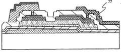
在包括反交错型薄膜晶体管的发光装置的反交错型薄膜晶体管中,在栅电极上形成栅极绝缘膜,在栅极绝缘膜上形成用作沟道形成区域的微晶半导体膜(也称为半非晶半导体膜),在微晶半导体膜上形成缓冲层,在缓冲层上形成一对源区域及漏区域,以使源区域及漏区域的一部分露出的方式形成与源区域及漏区域接触的一对源电极及漏电极。因此,源区域及漏区域具有与源电极及漏电极接触的区域和不与源电极及漏电极接触的区域。此外,在源电极及漏电极的外侧,源区域及漏区域的一部分、以及缓冲层的一部分露出。此外,在源电极及漏电极的端部的外侧形成源区域及漏区域的端部、以及缓冲层的端部。In an inverted staggered thin film transistor of a light emitting device including an inverted staggered thin film transistor, a gate insulating film is formed on a gate electrode, and a microcrystalline semiconductor film (also referred to as a channel formation region) is formed on the gate insulating film. Semi-amorphous semiconductor film), a buffer layer is formed on the microcrystalline semiconductor film, a pair of source region and drain region are formed on the buffer layer, and a part of the source region and drain region is exposed to form a contact with the source region and the drain region. A pair of source and drain electrodes. Therefore, the source region and the drain region have a region in contact with the source electrode and the drain electrode and a region not in contact with the source electrode and the drain electrode. In addition, a part of the source region and the drain region and a part of the buffer layer are exposed outside the source electrode and the drain electrode. In addition, the ends of the source region and the drain region and the end of the buffer layer are formed outside the ends of the source electrode and the drain electrode.
通过源电极及漏电极的端部和源区域及漏区域的端部不一致,并在源电极及漏电极的端部的外侧形成源区域及漏区域的端部,源电极及漏电极的端部之间的距离变长,从而可以防止源电极及漏电极之间的漏电流及短路。Since the ends of the source electrode and the drain electrode are inconsistent with the ends of the source region and the drain region, and the ends of the source region and the drain region are formed outside the ends of the source electrode and the drain electrode, the ends of the source electrode and the drain electrode The distance between them becomes longer, so that leakage current and short circuit between the source electrode and the drain electrode can be prevented.
此外,缓冲层的一部分具有凹部,并且该凹部的侧面与源区域及漏区域的端部一致。由于缓冲层的一部分具有凹部而源区域及漏区域之间的载流子移动的距离长,因此可以减少源区域及漏区域的之间产生的漏电流。In addition, a part of the buffer layer has a recess, and the side surfaces of the recess coincide with the ends of the source region and the drain region. Since a portion of the buffer layer has a concave portion, the distance for carriers to move between the source region and the drain region is long, thereby reducing leakage current generated between the source region and the drain region.
此外,在微晶半导体膜和源区域及漏区域之间形成有缓冲层。微晶半导体膜用作沟道形成区域。另外,缓冲层在防止微晶半导体膜的氧化的同时用作高电阻区域。在微晶半导体膜和源区域及漏区域之间使用高电阻率的非晶半导体膜形成有缓冲层。由此,本发明的薄膜晶体管的电场效应迁移率高,且截止时(即,对栅电极施加负电压时)的漏电流少,而漏耐压性高。In addition, a buffer layer is formed between the microcrystalline semiconductor film and the source and drain regions. The microcrystalline semiconductor film is used as a channel formation region. In addition, the buffer layer serves as a high-resistance region while preventing oxidation of the microcrystalline semiconductor film. A buffer layer is formed using a high-resistivity amorphous semiconductor film between the microcrystalline semiconductor film and the source and drain regions. Accordingly, the thin film transistor of the present invention has high field effect mobility, low leakage current at off time (that is, when a negative voltage is applied to the gate electrode), and high drain withstand voltage.
采用非晶半导体膜作为缓冲层。再者,优选采用包含氮、氢、卤素的任何一种以上的非晶半导体膜。通过非晶半导体膜包含氮、氢、卤素的任何一种,可以减少包含在微晶半导体膜中的晶粒的氧化。An amorphous semiconductor film is used as a buffer layer. Furthermore, it is preferable to use an amorphous semiconductor film containing any one or more of nitrogen, hydrogen, and halogen. When the amorphous semiconductor film contains any of nitrogen, hydrogen, and halogen, oxidation of crystal grains included in the microcrystalline semiconductor film can be reduced.
可以通过等离子体CVD法、溅射法等形成缓冲层。此外,在形成非晶半导体膜之后,通过对于非晶半导体膜进行使用氮等离子体、氢等离子体、或卤素等离子体的处理,来可以使非晶半导体膜氮化、氢化、或卤化。The buffer layer can be formed by a plasma CVD method, a sputtering method, or the like. In addition, after forming the amorphous semiconductor film, the amorphous semiconductor film can be nitrided, hydrogenated, or halogenated by treating the amorphous semiconductor film with nitrogen plasma, hydrogen plasma, or halogen plasma.
通过在微晶半导体膜的表面上设置缓冲层来可以减少包含在微晶半导体膜中的晶粒的氧化,因此可以减少薄膜晶体管的电特性的退化。Oxidation of crystal grains contained in the microcrystalline semiconductor film can be reduced by providing a buffer layer on the surface of the microcrystalline semiconductor film, and thus degradation of electrical characteristics of the thin film transistor can be reduced.
与多晶半导体膜不同,微晶半导体膜可以直接形成在衬底上。具体而言,可以将氢化硅作为原料气体并使用等离子体CVD装置来形成。通过上述方法制造的微晶半导体膜也包括在非晶半导体中含有0.5nm至20nm的晶粒的微晶半导体膜。因此,与使用多晶半导体膜的情况不同,不需要在形成半导体膜之后进行晶化工序。可以缩减制造薄膜晶体管时的工序数,并且还可以提高发光装置的成品率并抑制成本。此外,使用频率为1GHz以上的微波的等离子体具有高电子密度,从而容易离解原料气体的氢化硅。因此,通过使用频率为1GHz以上的微波的等离子体CVD法,与频率为几十MHz至几百MHz的微波等离子体CVD法相比,可以较容易制造微晶半导体膜,并可以提高成膜速度。因而,可以提高发光装置的批量生产性。Unlike polycrystalline semiconductor films, microcrystalline semiconductor films can be directly formed on a substrate. Specifically, silicon hydride can be used as a source gas and formed using a plasma CVD apparatus. The microcrystalline semiconductor film produced by the above method also includes a microcrystalline semiconductor film containing crystal grains of 0.5 nm to 20 nm in an amorphous semiconductor. Therefore, unlike the case of using a polycrystalline semiconductor film, it is not necessary to perform a crystallization process after forming the semiconductor film. The number of steps in manufacturing a thin film transistor can be reduced, and the yield of the light-emitting device can be improved and the cost can be suppressed. In addition, plasma using microwaves with a frequency of 1 GHz or higher has a high electron density and easily dissociates silicon hydride which is a source gas. Therefore, the plasma CVD method using microwaves with a frequency of 1 GHz or higher can produce a microcrystalline semiconductor film more easily and increase the film formation speed compared with the microwave plasma CVD method with a frequency of several tens of MHz to several hundreds of MHz. Therefore, mass productivity of the light emitting device can be improved.
此外,将微晶半导体膜用于沟道形成区域,制造薄膜晶体管(TFT),并且将该薄膜晶体管使用于像素部、驱动电路来制造发光装置。将微晶半导体膜用于沟道形成区域的薄膜晶体管的电场效应迁移率为1cm2/V·sec至20cm2/V·sec,其是将非晶半导体膜用于沟道形成区域的薄膜晶体管的2倍至20倍。因此可以将驱动电路的一部分或全部形成于与像素部相同的衬底上,来形成系统型面板(system onpanel)。In addition, a thin film transistor (TFT) is produced by using a microcrystalline semiconductor film in a channel formation region, and a light emitting device is produced by using the thin film transistor in a pixel portion and a driver circuit. Field effect mobility of a thin film transistor using a microcrystalline semiconductor film in a channel forming region is 1 cm2 /V·sec to 20 cm2 /V·sec, which is a thin film transistor using an amorphous semiconductor film in a
此外,发光装置包括发光元件。在发光元件的范围中,包括由电流或电压控制亮度的元件。具体而言,包括无机EL(Electro Luminescence;电致发光)、有机EL等。In addition, the light emitting device includes a light emitting element. Within the scope of light-emitting elements are included elements whose brightness is controlled by current or voltage. Specifically, inorganic EL (Electro Luminescence; electroluminescence), organic EL, and the like are included.
另外,发光装置还包括发光元件处于密封状态的面板、以及处于将包括控制器的IC等安装在该面板上的状态的模块。再者,本发明涉及对于制造该发光装置的过程中的相当于发光元件完成之前的一个方式的元件衬底,该元件衬底的多个像素的各个中具备将电流供给给发光元件的单元。元件衬底采用各种方式,既可以处于只形成有发光元件的像素电极的状态,又可以处于在形成成为像素电极的导电膜之后并进行蚀刻来形成像素电极之前的状态。In addition, the light-emitting device also includes a panel in which a light-emitting element is sealed, and a module in which an IC including a controller is mounted on the panel. Furthermore, the present invention relates to an element substrate in an embodiment corresponding to before the completion of the light-emitting element in the process of manufacturing the light-emitting device, wherein each of the plurality of pixels of the element substrate is provided with a unit for supplying current to the light-emitting element. The element substrate may be formed in various forms, and may be in a state where only the pixel electrodes of the light-emitting elements are formed, or may be in a state before forming the pixel electrodes by etching after forming the conductive film to be the pixel electrodes.
注意,本说明书中的发光装置是指图像显示器件、发光器件、或光源(包括照明装置)。此外,如下模块也都包括在发光装置中:安装有连接器如FPC(柔性印刷衬底)、TAB(带式自动接合)胶带、或TCP(带载封装)的模块;TAB胶带及TCP的前端设置有印刷布线板的模块;或通过COG(晶玻接装,chip on glass)方式将IC(集成电路)直接安装在发光元件中的模块。Note that a light emitting device in this specification refers to an image display device, a light emitting device, or a light source (including a lighting device). In addition, the following modules are also included in the light-emitting device: a module mounted with a connector such as FPC (flexible printed substrate), TAB (tape automated bonding) tape, or TCP (tape carrier package); front end of TAB tape and TCP A module provided with a printed wiring board; or a module in which an IC (integrated circuit) is directly installed in a light-emitting element by means of COG (chip on glass).
根据本发明,可以批量生产性高地制造包括电特性良好且可靠性高的薄膜晶体管的发光装置。According to the present invention, a light-emitting device including a thin film transistor having good electrical characteristics and high reliability can be manufactured with high mass productivity.
附图说明Description of drawings
图1A和1B是说明本发明的发光装置的制造方法的截面图;1A and 1B are cross-sectional views illustrating a method of manufacturing a light emitting device of the present invention;
图2A至2C是说明本发明的发光装置的制造方法的截面图;2A to 2C are cross-sectional views illustrating a method of manufacturing a light emitting device of the present invention;
图3A和3B是说明本发明的发光装置的制造方法的截面图;3A and 3B are cross-sectional views illustrating a method of manufacturing a light emitting device of the present invention;
图4A和4B是说明本发明的发光装置的制造方法的截面图;4A and 4B are cross-sectional views illustrating a method of manufacturing a light emitting device of the present invention;
图5A至5C是说明本发明的发光装置的制造方法的俯视图;5A to 5C are top views illustrating a method of manufacturing a light emitting device of the present invention;
图6A至6C是说明本发明的发光装置的制造方法的截面图;6A to 6C are cross-sectional views illustrating a method of manufacturing a light emitting device of the present invention;
图7A至7C是说明本发明的发光装置的制造方法的截面图;7A to 7C are cross-sectional views illustrating a method of manufacturing a light emitting device of the present invention;
图8A和8B是说明本发明的发光装置的制造方法的截面图;8A and 8B are cross-sectional views illustrating a method of manufacturing a light emitting device of the present invention;
图9A至9D是说明本发明的发光装置的制造方法的俯视图;9A to 9D are top views illustrating a method of manufacturing a light-emitting device of the present invention;
图10是说明本发明的微波等离子体CVD装置的俯视图;Fig. 10 is a plan view illustrating a microwave plasma CVD apparatus of the present invention;
图11A至11D是说明可以应用于本发明的多灰度级掩模的图;11A to 11D are diagrams illustrating a multi-grayscale mask that can be applied to the present invention;
图12A至12C是说明本发明的显示面板的透视图;12A to 12C are perspective views illustrating a display panel of the present invention;
图13A至13D是说明使用本发明的发光装置的电子设备的透视图;13A to 13D are perspective views illustrating electronic equipment using the light emitting device of the present invention;
图14是说明使用本发明的发光装置的电子设备的图;14 is a diagram illustrating an electronic device using the light emitting device of the present invention;
图15A和15B是说明本发明的发光装置的制造方法的截面图;15A and 15B are cross-sectional views illustrating a method of manufacturing a light-emitting device of the present invention;
图16A至16C是说明可以应用于本发明的发光装置的像素的截面图;16A to 16C are cross-sectional views illustrating pixels that can be applied to a light emitting device of the present invention;
图17A和17B是说明本发明的发光显示面板的俯视图及截面图;17A and 17B are top and cross-sectional views illustrating a light-emitting display panel of the present invention;
图18是说明本发明的发光装置的结构的框图;18 is a block diagram illustrating the structure of the light emitting device of the present invention;
图19是说明本发明的发光装置的驱动电路的结构的等效电路图;19 is an equivalent circuit diagram illustrating the structure of a driving circuit of the light emitting device of the present invention;
图20是说明本发明的发光装置的驱动电路的结构的等效电路图;20 is an equivalent circuit diagram illustrating the structure of a driving circuit of a light emitting device of the present invention;
图21是说明本发明的发光装置的驱动电路的布局的俯视图;21 is a plan view illustrating the layout of the driving circuit of the light emitting device of the present invention;
图22A和22B是示出通过拉曼光谱法检测微晶半导体膜的结果的图;22A and 22B are graphs showing the results of detecting a microcrystalline semiconductor film by Raman spectroscopy;
图23是用于器件模拟的模型图;Figure 23 is a model diagram for device simulation;
图24是示出根据器件模拟得到的电流电压特性的图;FIG. 24 is a graph showing current-voltage characteristics obtained from device simulations;
图25A和25B是示出根据器件模拟得到的薄膜晶体管的电子浓度分布的图。25A and 25B are graphs showing electron concentration distributions of thin film transistors obtained from device simulations.
本发明的选择图为图2A至2C。A selection diagram of the present invention is shown in Figures 2A to 2C.
具体实施方式Detailed ways
下面,关于本发明的实施方式将参照附图给予说明。但是,所属技术领域的普通技术人员可以很容易地理解一个事实,就是本发明可以以多个不同形式来实施,其方式和详细内容可以被变换为各种各样的形式而不脱离本发明的宗旨及其范围。因此,本发明不应该被解释为仅限定在本实施方式所记载的内容中。Hereinafter, embodiments of the present invention will be described with reference to the drawings. However, those skilled in the art can easily understand the fact that the present invention can be implemented in many different forms, and its modes and details can be changed into various forms without departing from the spirit of the present invention. purpose and scope. Therefore, the present invention should not be interpreted as being limited only to the contents described in this embodiment mode.
实施方式1
在本实施方式中,对于用于发光装置的薄膜晶体管的制造工序,参照图1A至图12C进行说明。图1A至图4B、图6A至图8B是示出薄膜晶体管的制造工序的截面图,而图5A至5C以及图9A至9D是一个像素中的薄膜晶体管及像素电极的连接区域的俯视图。In this embodiment mode, a manufacturing process of a thin film transistor used in a light-emitting device will be described with reference to FIGS. 1A to 12C . FIGS. 1A to 4B and FIGS. 6A to 8B are cross-sectional views illustrating the manufacturing process of a thin film transistor, and FIGS. 5A to 5C and FIGS. 9A to 9D are plan views of a connection region between a thin film transistor and a pixel electrode in one pixel.
具有微晶半导体膜的n型薄膜晶体管更优选用于驱动电路,因为其电场效应迁移率高于具有微晶半导体膜的p型薄膜晶体管的迁移率。优选使形成在相同衬底上的所有薄膜晶体管的极性为相同,以抑制工序数的增加。在此,使用n沟道型的薄膜晶体管来进行说明。An n-type thin film transistor having a microcrystalline semiconductor film is more preferably used for a driving circuit because its electric field effect mobility is higher than that of a p-type thin film transistor having a microcrystalline semiconductor film. It is preferable to make the polarity of all the thin film transistors formed on the same substrate the same in order to suppress an increase in the number of steps. Here, an n-channel type thin film transistor will be used for description.
如图1A所示,在衬底50上形成栅电极51。衬底50可以使用通过熔化方法或浮发方法(float method)制造的无碱玻璃衬底例如钡硼硅酸盐玻璃、铝硼硅酸盐玻璃、铝硅酸盐玻璃等、或陶瓷衬底,还可以使用具有可承受本制造工序的处理温度的耐热性的塑料衬底等。此外,还可以使用在不锈钢合金等金属衬底表面上设置绝缘膜的衬底。在衬底50是母玻璃的情况下,其尺寸可以采用第一代(320mm×400mm)、第二代(400mm×500mm)、第三代(550mm×650mm)、第四代(680mm×880mm或730mm×920mm)、第五代(1000mm×1200mm或1100mm×1250mm)、第六代(1500mm×1800mm)、第七代(1900mm×2200mm)、第八代(2160mm×2460mm)、第九代(2400mm×2800mm或2450mm×3050mm)、第十代(2950mm×3400mm)等。As shown in FIG. 1A , a
使用钛、钼、铬、钽、钨、铝等的金属材料或其合金材料形成栅电极51。可以通过溅射法、真空蒸镀法在衬底50上形成导电膜,通过光刻技术或喷墨法在该导电膜上形成掩模,并使用该掩模蚀刻导电膜,来形成栅电极51。注意,作为用来提高栅电极51的紧密性并防止扩散到基底的阻挡金属,也可以将上述金属材料的氮化物膜设置在衬底50和栅电极51之间。在此,通过采用使用第一光掩模形成的抗蚀剂掩模来蚀刻形成在衬底50上的导电膜,来形成栅电极51。The
注意,因为在栅电极51上形成绝缘膜、半导体膜及布线等,所以其端部优选加工为锥形形状,以便防止断开。此外,虽然未图示,但可以通过该工序同时形成连接到栅电极的布线。Note that since an insulating film, a semiconductor film, wiring, and the like are formed on the
其次,在栅电极51上按顺序形成栅极绝缘膜52a、52b、微晶半导体膜53、缓冲层54、以及添加有赋予一导电型的杂质元素的半导体膜55、导电膜65a至65c。接着,在导电膜65c上涂敷抗蚀剂80。注意,优选至少连续形成栅极绝缘膜52a、52b、微晶半导体膜53及缓冲层54。再者,优选连续形成栅极绝缘膜52a、52b、微晶半导体膜53、缓冲层54、以及添加有赋予一导电型的杂质元素的半导体膜55。通过在不接触大气的状态下至少连续形成栅极绝缘膜52a、52b、微晶半导体膜53、及缓冲层54,可以形成各个叠层界面而不被大气成分及悬浮在大气中的污染杂质元素污染,因此可以减少薄膜晶体管特性的不均匀。Next,
栅极绝缘膜52a、52b分别可以通过CVD法或溅射法等并使用氧化硅膜、氮化硅膜、氧氮化硅膜、或氮氧化硅膜来形成。在此示出,按顺序层叠氧化硅膜或氧氮化硅膜、和氮化硅膜或氮氧化硅膜来形成栅极绝缘膜52a、52b的方式。另外,栅极绝缘膜还可以不采用两层结构,而从衬底一侧按顺序层叠氮化硅膜或氮氧化硅膜、氧化硅膜或氧氮化硅膜、和氮化硅膜或氮氧化硅膜的三层来形成栅极绝缘膜。此外,还可以使用氧化硅膜、氮化硅膜、氧氮化硅膜或者氮氧化硅膜的单层来形成栅极绝缘膜。The
在此,氧氮化硅膜是指具有如下组成的膜:氧的含有量比氮的含有量多,并且在采用卢瑟福背散射光谱学法(RBS:Rutherford BackscatteringSpectrometry)以及氢前方散射法(HFS:Hydrogen Forward Scattering)检测时,作为浓度范围,包含50原子%至70原子%的氧,包含0.5原子%至15原子%的氮,包含25原子%至35原子%的硅,包含0.1原子%至10原子%的氢。此外,氮氧化硅膜是指具有如下组成的膜:氮的含量比氧的含量多,并且在采用RBS及HFS检测时,作为浓度范围,包含5原子%至30原子%的氧,包含20原子%至55原子%的氮,包含25原子%至35原子%的硅,包含10原子%至30原子%的氢。但是,在构成氧氮化硅或氮氧化硅的原子的总和为100原子%时,氮、氧、硅及氢的含有比率包括在上述范围内。Here, the silicon oxynitride film refers to a film having a composition in which the content of oxygen is larger than the content of nitrogen, and is obtained by Rutherford Backscattering Spectroscopy (RBS: Rutherford Backscattering Spectrometry) and Hydrogen Front Scattering ( HFS: Hydrogen Forward Scattering) detection, as a concentration range, containing 50 atomic % to 70 atomic % of oxygen, containing 0.5 atomic % to 15 atomic % of nitrogen, containing 25 atomic % to 35 atomic % of silicon, containing 0.1 atomic % to 10 at% hydrogen. In addition, the silicon oxynitride film refers to a film having a composition in which the content of nitrogen is larger than the content of oxygen, and when detected by RBS and HFS, the concentration range includes 5 atomic % to 30 atomic % of oxygen, including 20 atomic % % to 55 atomic % nitrogen, containing 25 atomic % to 35 atomic % silicon, containing 10 atomic % to 30 atomic % hydrogen. However, when the sum of atoms constituting silicon oxynitride or silicon oxynitride is 100 atomic %, the content ratios of nitrogen, oxygen, silicon, and hydrogen are included in the above-mentioned ranges.
微晶半导体膜53是指包括非晶结构和结晶结构(包括单晶、多晶)之间的中间结构的半导体的膜。该半导体为具有在自由能方面上很稳定的第三状态的半导体,并且具有短程有序且具有晶格应变的结晶质的半导体,粒径为0.5nm至20nm的柱状或针状结晶在对于衬底表面成为法线的方向上生长。此外,微晶半导体与非晶半导体混合在一起。在微晶半导体的典型例子的微晶硅中,其拉曼光谱转移到比表示单晶硅的521cm-1低波数一侧。即,微晶硅的拉曼光谱的峰值位于表示单晶硅的521cm-1和表示非晶硅的480cm-1之间。此外,包含有至少1原子%或更多的氢或卤素,以便终止悬空键。再者,可以通过将氦、氩、氪、氖等的稀有气体元素包含在微晶半导体膜中而进一步促进晶格应变来提高稳定性以获得良好的微晶半导体膜。关于这种微晶半导体膜的记述例如在美国专利文件4,409,134号中公开。The
可以通过使用频率为几十MHz至几百MHz的高频率等离子体CVD法、或频率为1GHz以上的微波等离子体CVD装置形成该微晶半导体膜。代表性地,可以使用氢稀释SiH4、Si2H6等的氢化硅形成。另外,除了使用氢化硅及氢之外,还可以使用选自氦、氩、氪、氖中的一种或多种稀有气体元素进行稀释,来形成微晶半导体膜。将氢的流量比设定为此时的氢化硅的50倍以上1000倍以下,优选设定为50倍以上200倍以下,更优选为100倍。注意,也可以使用SiH2Cl2、SiHCl3、SiCl4、SiF4等代替氢化硅。The microcrystalline semiconductor film can be formed by using a high-frequency plasma CVD method with a frequency of several tens of MHz to several hundreds of MHz, or a microwave plasma CVD apparatus with a frequency of 1 GHz or more. Representatively, hydrogenated silicon formation of SiH4 , Si2 H6 , etc. may be diluted with hydrogen. In addition, in addition to silicon hydride and hydrogen, one or more rare gas elements selected from helium, argon, krypton, and neon can be diluted to form a microcrystalline semiconductor film. The flow ratio of hydrogen is set to 50 times to 1000 times that of silicon hydride at this time, preferably 50 times to 200 times, more preferably 100 times. Note that SiH2 Cl2 , SiHCl3 , SiCl4 , SiF4 , etc. may also be used instead of silicon hydride.
此外,由于当示意性地不添加用于价电子控制的杂质元素时,微晶半导体膜呈现弱n型导电性,因此可以通过在形成膜的同时或形成膜之后对于用作薄膜晶体管的沟道形成区域的微晶半导体膜添加赋予p型的杂质元素,来控制阈值。作为赋予p型的杂质元素的典型,可举出硼,优选将B2H6、BF3等的杂质气体以1ppm至1000ppm的比例,优选以1ppm至100ppm的比例混入到氢化硅中。而且,硼的浓度例如优选为1×10014atoms/cm3至6×1016atoms/cm3。In addition, since the microcrystalline semiconductor film exhibits weak n-type conductivity when an impurity element for valence electron control is schematically not added, it is possible to control the channel functioning as a thin film transistor by simultaneously forming the film or after forming the film. A p-type impurity element is added to the microcrystalline semiconductor film forming the region to control the threshold value. Typical p-type impurity elements include boron, and impurity gases such as B2 H6 and BF3 are preferably mixed into silicon hydride at a ratio of 1 ppm to 1000 ppm, preferably at a ratio of 1 ppm to 100 ppm. Also, the concentration of boron is preferably, for example, 1×10014 atoms/cm3 to 6×10¹⁶ atoms/cm3 .
此外,微晶半导体膜的氧浓度优选为5×1019cm-3以下,更优选为1×1019cm-3以下,且氮及碳的浓度分别为3×1018cm-3以下。通过降低混入到微晶半导体膜中的氧、氮、及碳的浓度,可以防止微晶半导体膜的n型化。In addition, the oxygen concentration of the microcrystalline semiconductor film is preferably 5×1019 cm−3 or less, more preferably 1×1019 cm−3 or less, and the concentrations of nitrogen and carbon are each 3×1018 cm−3 or less. By reducing the concentration of oxygen, nitrogen, and carbon mixed into the microcrystalline semiconductor film, n-type conversion of the microcrystalline semiconductor film can be prevented.
微晶半导体膜53以厚于0nm至200nm以下的厚度,优选以1nm以上100nm以下的厚度,更优选以5nm以上50nm以下的厚度形成。微晶半导体膜53用作后面形成的薄膜晶体管的沟道形成区域。通过以5nm以上50nm的范围内的厚度形成微晶半导体膜53,后面形成的薄膜晶体管成为完全耗尽型。此外,因为微晶半导体膜53的成膜速度比非晶半导体膜慢,即为非晶半导体膜的成膜速度的1/10至1/100,所以通过减薄膜厚度,可以提高生产率。由于微晶半导体膜由微晶构成,因此其电阻比非晶半导体膜低。由此,在将微晶半导体膜用于沟道形成区域的薄膜晶体管中表示电流电压特性的曲线的上升部分的倾斜急剧,其作为开关元件的响应性优良且可以进行高速驱动。此外,通过将微晶半导体膜用于薄膜晶体管的沟道形成区域,可以抑制薄膜晶体管的阈值变动。因此,可以制造电特性的不均匀少的发光装置。The
另外,微晶半导体膜的迁移率比非晶半导体膜高。因此,通过使用其沟道形成区域由微晶半导体膜形成的薄膜晶体管作为发光元件的开关,可以缩小沟道形成区域的面积,即薄膜晶体管的面积。由此,在每一个像素中薄膜晶体管所占的面积缩小,可以提高像素的开口率。结果,可以制造分辨率高的装置In addition, the mobility of the microcrystalline semiconductor film is higher than that of the amorphous semiconductor film. Therefore, by using a thin film transistor whose channel formation region is formed of a microcrystalline semiconductor film as a switch of a light emitting element, the area of the channel formation region, that is, the area of the thin film transistor can be reduced. Therefore, the area occupied by the thin film transistor in each pixel is reduced, and the aperture ratio of the pixel can be increased. As a result, devices with high resolution can be fabricated
可以通过使用SiH4、Si2H6等的氢化硅并采用等离子体CVD法形成缓冲层54。此外,可以对上述氢化硅添加选自氦、氩、氪、氖中的一种或多种的稀有气体元素进行稀释形成非晶半导体膜。通过使用其流量为氢化硅的流量的1倍以上20倍以下,优选为1倍以上10倍以下,更优选为1倍以上5倍以下的氢,可以形成包含氢的非晶半导体膜。此外,通过使用上述氢化硅和氮或氨,可以形成包含氮的非晶半导体膜。另外,通过使用上述氢化硅和包含氟、氯、溴、或碘的气体(F2、Cl2、Br2、I2、HF、HCl、HBr、HI等),可以形成包含氟、氯、溴、或碘的非晶半导体膜。注意,可以使用SiH2Cl2、SiHCl3、SiCl4、SiF4等。The
此外,作为缓冲层54,可以将非晶半导体用作靶子并使用氢或稀有气体进行溅射来形成非晶半导体膜。此时,通过将氨、氮、或N2O包含在气氛中,可以形成含有氮的非晶半导体膜。另外,通过将含有氟、氯、溴、或碘的气体(F2、Cl2、Br2、I2、HF、HCl、HBr、HI等)包含在气氛中,可以形成含有氟、氯、溴、或碘的非晶半导体膜。In addition, as the
此外,作为缓冲层54,也可以在微晶半导体膜53的表面上采用等离子体CVD法或溅射法形成非晶半导体膜,然后对非晶半导体膜的表面进行使用氢等离子体、氮等离子体、或卤素等离子体的处理,来使非晶半导体膜表面氢化、氮化、或卤化。或者,也可以对非晶半导体膜的表面进行使用氦等离子体、氖等离子体、氩等离子体、氪等离子体等的处理。In addition, as the
优选使用不包含晶粒的非晶半导体膜形成缓冲层54。因此,在采用频率为几十MHz至几百MHz的高频等离子体CVD法、或微波等离子体CVD法形成非晶半导体膜的情况下,优选控制成膜条件以使它成为不包含晶粒的非晶半导体膜。
缓冲层54的一部分有时会在后面的源区域及漏区域的形成过程中被蚀刻,从而缓冲层54优选以在蚀刻之后其一部分残留的厚度来形成。典型地说,优选以150nm以上200nm以下的厚度形成缓冲层54。A part of the
注意,缓冲层54优选不添加有赋予一导电型的杂质元素如磷、硼等。尤其是,用来控制阈值包含在微晶半导体膜中的硼、或包含在添加有赋予一导电型的杂质元素的半导体膜中的磷优选不混入在缓冲层54中。结果,通过消除PN结所导致的漏电流的产生区域,可以实现漏电流的减少。此外,通过在添加有赋予一导电型的杂质元素的半导体膜和微晶半导体膜之间形成不添加有赋予一导电型的杂质元素如磷、硼等的非晶半导体膜,可以防止分别包含在微晶半导体膜和源区域及漏区域中的杂质扩散。Note that the
通过在微晶半导体膜53的表面上形成非晶半导体膜,进一步形成包含氢、氮、或卤素的非晶半导体膜,来可以防止包含在微晶半导体膜53的晶粒表面的自然氧化。特别是,在非晶半导体和微晶粒相接触的区域中,因受局部应力而容易产生裂缝。当该裂缝与氧接触时产生晶粒的氧化,并形成氧化硅。然而,通过在微晶半导体膜53的表面上形成缓冲层,可以防止微晶粒的氧化。此外,通过形成缓冲层,可以防止当后面形成源区域及漏区域之际产生的蚀刻残渣混入到微晶半导体膜中。By forming an amorphous semiconductor film on the surface of the
此外,使用非晶半导体膜或使用包含氢、氮、或卤素的非晶半导体膜形成缓冲层54。因此非晶半导体膜的能隙比微晶半导体膜的能隙大(非晶半导体膜的能隙为1.1eV至1.5eV,而微晶半导体膜的能隙为1.6eV至1.8eV),电阻高,并且迁移率低,即为微晶半导体膜的1/5至1/10。由此,在后面形成的薄膜晶体管中,形成在源区域及漏区域和微晶半导体膜之间的缓冲层用作高电阻区域,而微晶半导体膜用作沟道形成区域。因此,可以减少薄膜晶体管的截止电流。当将该薄膜晶体管用作发光装置的开关元件时,可以提高发光装置的对比度。Further, the
在形成n沟道型薄膜晶体管的情况下,添加磷作为典型杂质元素,即对于氢化硅添加PH3等的杂质气体,来形成添加有赋予一导电型的杂质元素的半导体膜55,即可。此外,在形成p沟道型薄膜晶体管的情况下,添加硼作为典型杂质元素即可,即对于氢化硅添加B2H6等的杂质气体即可。可以使用微晶半导体膜或非晶半导体膜形成添加有赋予一导电型的杂质元素的半导体膜55。再者,也可以使用添加有赋予一导电型的杂质的非晶半导体膜和添加有赋予一导电型的杂质的微晶半导体膜的叠层形成添加有赋予一导电型的杂质元素的半导体膜55。通过在缓冲层54一侧形成添加有赋予一导电型的杂质元素的非晶半导体膜,并在其上形成添加有赋予一导电型的杂质元素的微晶半导体膜,电阻逐渐变化,所以载流子容易流过,而可以提高迁移率。以2nm以上50nm以下的厚度形成添加有赋予一导电型的杂质元素的半导体膜55。通过减薄添加有赋予一导电型的杂质元素的半导体膜的膜厚度,可以提高生产率。When forming an n-channel thin film transistor, phosphorus is added as a typical impurity element, that is, an impurity gas such as PH3 is added to silicon hydride to form the
在此,参照图10示出一种等离子体CVD装置,该微波等离子体CVD装置能够连续进行从形成栅极绝缘膜52a、52b的步骤到形成添加有赋予一导电型的杂质元素的半导体膜55。图10是示出等离子体CVD装置的俯视截面的示意图,其具有在公共室1120的周围具备装载室1110、卸载室1115、反应室(1)1111至反应室(4)1114的结构。在公共室1120和每个室之间具备闸阀1122至1127,以防止在每个室内进行的处理互相干涉。衬底装载在装载室1110、卸载室1115的盒子1128、1129,然后由公共室1120的传送单元1121传送到反应室(1)1111至反应室(4)1114。该微波等离子体CVD装置能够对于每个堆积膜种类分配反应室,从而可以在不与大气接触的状态下连续形成多个不同的覆盖膜。Here, referring to FIG. 10, there is shown a plasma CVD apparatus capable of continuously performing the steps from forming the
在反应室(1)至反应室(4)的各个中,分别层叠形成栅极绝缘膜52a、52b、微晶半导体膜53、缓冲层54、以及添加有赋予一导电型的杂质元素的半导体膜55。在此情况下,通过转换原料气体,可以连续地层叠多个不同种类的膜。在此情况下,形成栅极绝缘膜,然后将硅烷等的氢化硅引入到反应室内,使残留氧及氢化硅反应,并将反应物排出到反应室的外部,从而可以降低反应室内的残留氧浓度。结果,可以降低包含在微晶半导体膜中的氧浓度。此外,可以防止包含在微晶半导体膜中的晶粒的氧化。In each of the reaction chamber (1) to the reaction chamber (4), the
或者,在反应室(1)及反应室(3)中形成栅极绝缘膜52a、52b、微晶半导体膜53、以及缓冲层54,而在反应室(2)及反应室(4)中形成添加有赋予一导电型的杂质元素的半导体膜55。通过只使用赋予一导电型的杂质单独地进行成膜,可以防止残留在反应室中的赋予一导电型的杂质元素混入到其他膜中。Alternatively, the
像这样,由于可以使用连接有多个反应室的微波等离子体CVD装置同时形成栅极绝缘膜52a、52b、微晶半导体膜53、缓冲层54、以及添加有赋予一导电型的杂质元素的半导体膜55,因此提高批量生产性。此外,即使在某个反应室中进行维护及清洗,也可以在其他反应室中形成膜,从而可以缩短成膜周期(cycle time)。另外,因为可以在不被大气成分及悬浮在大气中的污染杂质元素污染的状态下形成各个叠层界面,所以可以减少薄膜晶体管的特性的不均匀。In this way, since the
此外,可以在反应室(1)中形成栅极绝缘膜52a、52b,在反应室(2)中形成微晶半导体膜53及缓冲层54,在反应室(3)中形成添加有赋予一导电型的杂质元素的半导体膜55。另外,在使用氧化硅膜或氧氮化硅膜形成栅极绝缘膜52a,并使用氮化硅膜或氮氧化硅膜形成栅极绝缘膜52b的情况下,也可以设置五个反应室,并且在反应室(1)中形成栅极绝缘膜52a的氧化硅膜或氧氮化硅膜,在反应室(2)中形成栅极绝缘膜52b的氮化硅膜或氮氧化硅膜,在反应室(3)中形成微晶半导体膜,在反应室(4)中形成缓冲层,在反应室(5)中形成添加有赋予一导电型的杂质元素的半导体膜。此外,因为微晶半导体膜的成膜速度较慢,所以也可以在多个反应室中形成微晶半导体膜。例如,也可以在反应室(1)中形成栅极绝缘膜52a、52b,在反应室(2)及(3)中形成微晶半导体膜53,在反应室(4)中形成缓冲层54,在反应室(5)中形成添加有赋予一导电型的杂质元素的半导体膜55。像这样,通过在多个反应室中同时形成微晶半导体膜53,可以提高生产率。注意,此时优选使用要形成的种类的膜涂敷各个反应室的内壁。In addition, the
由于当使用这种结构的等离子体CVD装置时,可以在各个反应室中形成类似种类的膜或一种膜,并且在不暴露在大气的状态下连续形成上述膜,因此可以在不被已形成的膜的残留物及悬浮在大气中的杂质元素污染的状态下形成各个叠层界面。Since when using the plasma CVD apparatus of this structure, a similar kind of film or a film can be formed in each reaction chamber, and the above-mentioned film can be continuously formed in a state not exposed to the atmosphere, so it is possible to Each stack interface is formed under the contamination state of film residues and impurity elements suspended in the atmosphere.
注意,虽然在图10所示的等离子体CVD装置中分别设置有装载室及卸装室,但是也可以设置一个装载/卸装室。此外,在微波等离子体CVD装置中也可以设置备用室。由于可以通过在备用室中对衬底进行预热而在各个反应室中缩短到形成膜的加热时间,因此可以提高生产率。Note that although a loading chamber and an unloading chamber are separately provided in the plasma CVD apparatus shown in FIG. 10, one loading/unloading chamber may be provided. In addition, a spare chamber may also be provided in the microwave plasma CVD apparatus. Since the heating time up to film formation can be shortened in each reaction chamber by preheating the substrate in the spare chamber, productivity can be improved.
下面,说明成膜处理。在这种成膜处理中,根据其目的而选择从气体供给部供给的气体,即可。Next, the film formation process will be described. In such a film forming process, the gas supplied from the gas supply unit may be selected according to the purpose.
在此,作为一例举出如下方法:形成氧氮化硅膜作为栅极绝缘膜52a,并形成氮氧化硅膜作为栅极绝缘膜52b。Here, as an example, a method of forming a silicon oxynitride film as the
首先,对于微波等离子体CVD装置的反应室的处理容器内部使用氟自由基进行清洗。注意,通过将氟化碳、氟化氮、或氟引入到设置在反应室外侧的等离子体产生器中并离解,然后将氟自由基引入到反应室中,可以对反应室进行清洗。First, the inside of the processing container in the reaction chamber of the microwave plasma CVD apparatus is cleaned with fluorine radicals. Note that the reaction chamber can be cleaned by introducing fluorinated carbon, nitrogen fluoride, or fluorine into a plasma generator provided outside the reaction chamber and dissociated, and then introducing fluorine radicals into the reaction chamber.
通过在使用氟自由基进行清洗之后,将大量的氢引入到反应室内,来使反应室内的残留氟和氢彼此反应,从而可以降低残留氟的浓度。由此,可以减少对于后面在反应室内壁形成的保护膜的氟混入量,并可以减薄保护膜的厚度。After cleaning with fluorine radicals, a large amount of hydrogen is introduced into the reaction chamber to cause residual fluorine and hydrogen in the reaction chamber to react with each other, thereby reducing the concentration of residual fluorine. Thereby, the amount of fluorine mixed into the protective film formed on the inner wall of the reaction chamber can be reduced, and the thickness of the protective film can be reduced.
接着,在反应室的处理容器的内壁的表面上堆积氧氮化膜作为保护膜。在此,处理容器内的压力为1Pa至200Pa,优选为1Pa至100Pa,并且引入氦、氩、氙、氪等的稀有气体的任何一种以上的气体作为等离子体点燃用气体。再者,引入稀有气体的任何一种及氢。特别是,优选使用氦作为等离子体点燃用气体,更优选使用氦和氢作为等离子体点燃用气体。Next, an oxynitride film is deposited as a protective film on the surface of the inner wall of the processing container in the reaction chamber. Here, the pressure in the processing container is 1 Pa to 200 Pa, preferably 1 Pa to 100 Pa, and any one or more of rare gases such as helium, argon, xenon, krypton is introduced as a gas for plasma ignition. Furthermore, any of rare gases and hydrogen are introduced. In particular, it is preferable to use helium as the gas for plasma ignition, and it is more preferable to use helium and hydrogen as the gas for plasma ignition.
氦的离子化能量较高,即为24.5eV。但是,由于准稳定状态位于大约20eV,因此在放电中可以以大约4eV进行离子化。由此,放电开始电压低,且容易维持放电。从而可以均匀地维持等离子体且实现节能。The ionization energy of helium is relatively high, namely 24.5eV. However, since the metastable state is at about 20eV, ionization can be performed at about 4eV in discharge. Accordingly, the discharge start voltage is low, and the discharge is easily maintained. Thereby, plasma can be maintained uniformly and energy saving can be achieved.
此外,也可以引入使用氦、氩、氙、氪等的稀有气体的任何一种以上及氧气体作为等离子体点燃用气体。通过将氧气体与稀有气体一起引入到处理容器中,可以容易进行等离子体的点燃。In addition, any one or more of rare gases such as helium, argon, xenon, and krypton and oxygen gas may be introduced as the gas for plasma ignition. Ignition of plasma can be easily performed by introducing oxygen gas into the processing container together with a rare gas.
接着,使电源装置的电源开启,并且在电源装置的输出为500W至6000W,优选为4000W至6000W的情况下产生等离子体。接着,将原料气体从气体供应部引入到处理容器内。具体而言,通过引入一氧化二氮、稀有气体、及硅烷作为原料气体,在处理容器的内壁表面上形成氧氮化硅膜作为保护膜。此时的氢化硅的流量为50sccm至300sccm,一氧化二氮的流量为500sccm至6000sccm,保护膜的膜厚度为500nm至2000nm。Next, the power of the power supply device is turned on, and plasma is generated with the output of the power supply device being 500W to 6000W, preferably 4000W to 6000W. Next, the source gas is introduced into the processing container from the gas supply unit. Specifically, a silicon oxynitride film is formed as a protective film on the inner wall surface of the processing container by introducing dinitrogen monoxide, a rare gas, and silane as source gases. At this time, the flow rate of silicon hydride is 50 sccm to 300 sccm, the flow rate of nitrous oxide is 500 sccm to 6000 sccm, and the film thickness of the protective film is 500 nm to 2000 nm.
接着,在停止原料气体的供给,降低处理容器内的压力,并使电源装置的电源关闭之后,将衬底设置在处理容器内的支架台上。Next, after the supply of the source gas is stopped, the pressure in the processing chamber is reduced, and the power of the power supply unit is turned off, the substrate is set on the holder in the processing chamber.
接着,通过与上述保护膜相同的工序,在衬底上堆积氧氮化硅膜作为栅极绝缘膜52a。Next, a silicon oxynitride film is deposited as a
在堆积预定的厚度的氧氮化硅膜之后,停止原料气体的供给,降低处理容器内的压力,并使电源装置的电源关闭。After depositing the silicon oxynitride film with a predetermined thickness, the supply of source gas is stopped, the pressure in the processing chamber is lowered, and the power of the power supply unit is turned off.
接着,处理容器内的压力为1Pa至200Pa,优选为1Pa至100Pa,作为等离子体点燃用气体,引入氦、氩、氙、氪等的稀有气体的任何一种以上、原料气体的硅烷、一氧化二氮、及氨。注意,作为原料气体,也可以引入氮代替氨。接着,使电源装置的电源开启,并且在电源装置的输出为500W至6000W,优选为4000W至6000W的情况下产生等离子体。接着,将原料气体从气体供应部引入到处理容器内,在衬底1130的氧氮化硅膜上形成氮氧化硅膜作为栅极绝缘膜52b。接着,停止原料气体的供给,降低处理容器内的压力,并使电源装置的电源关闭,来结束成膜过程。Next, the pressure in the processing container is 1Pa to 200Pa, preferably 1Pa to 100Pa, and as the gas for plasma ignition, any one or more of rare gases such as helium, argon, xenon, krypton, silane, monoxide, etc. Dinitrogen, and ammonia. Note that, as the raw material gas, nitrogen may also be introduced instead of ammonia. Next, the power of the power supply device is turned on, and plasma is generated with the output of the power supply device being 500W to 6000W, preferably 4000W to 6000W. Next, a source gas is introduced into the processing chamber from a gas supply unit, and a silicon oxynitride film is formed on the silicon oxynitride film of the
根据上述步骤,通过以反应室内壁的保护膜为氧氮化硅膜并在衬底上连续形成氧氮化硅膜及氮氧化硅膜,可以减少氧化硅等的杂质混入到上层一侧的氮氧化硅膜中。通过采用将能够产生微波的电源装置用作电源装置的微波等离子体CVD法形成上述膜,等离子体密度提高而可以形成高耐压性的膜。当将该膜用作栅极绝缘膜时,可以减少晶体管的阈值的不均匀。此外,可以提高BT特性。另外,对于静电的耐性提高,从而可以制造即使被施加高电压也不容易破坏的晶体管。而且,还可以制造随时间破坏少的晶体管、以及热载流子损坏少的晶体管。According to the above steps, by using the silicon oxynitride film as the protective film on the inner wall of the reaction chamber and continuously forming the silicon oxynitride film and the silicon oxynitride film on the substrate, it is possible to reduce impurities such as silicon oxide mixed into the nitrogen on the upper layer side. in the silicon oxide film. By forming the film by the microwave plasma CVD method using a power supply device capable of generating microwaves as a power supply device, the plasma density is increased and a film with high withstand voltage can be formed. When this film is used as a gate insulating film, variations in threshold value of transistors can be reduced. In addition, BT characteristics can be improved. In addition, the resistance to static electricity is improved, and a transistor that is not easily broken even when a high voltage is applied can be manufactured. Furthermore, transistors that are less damaged over time and transistors that are less damaged by hot carriers can also be manufactured.
此外,在将使用微波等离子体CVD装置形成的氧氮化硅膜的单层作为栅极绝缘膜的情况下,采用上述保护膜的形成方法及氧氮化硅膜的形成方法。特别是,通过将对于硅烷的一氧化二氮的流量比设定为50倍以上300倍以下,优选设定为50倍以上250倍以下,可以形成高耐压性的氧氮化硅膜。In addition, when a single layer of a silicon oxynitride film formed using a microwave plasma CVD apparatus is used as a gate insulating film, the above-described method of forming a protective film and the method of forming a silicon oxynitride film are employed. In particular, by setting the flow ratio of dinitrogen monoxide to silane to 50 times to 300 times, preferably 50 times to 250 times, a silicon oxynitride film with high withstand voltage can be formed.
接着,示出一种成膜处理方法,其中通过等离子体CVD法连续地形成微晶半导体膜及用作缓冲层非晶半导体膜。首先,与上述栅极绝缘膜同样地进行反应室的清洗。接着,在处理容器内堆积硅膜作为保护膜。在此,处理容器内的压力为1Pa至200Pa,优选为1Pa至100Pa,并且引入氦、氩、氙、氪等的稀有气体的任何一种以上的气体作为等离子体点燃用气体。此外,也可以与稀有气体一起引入氢。Next, a film formation processing method in which a microcrystalline semiconductor film and an amorphous semiconductor film used as a buffer layer are successively formed by a plasma CVD method is shown. First, the reaction chamber is cleaned in the same manner as the gate insulating film described above. Next, a silicon film is deposited as a protective film in the processing container. Here, the pressure in the processing container is 1 Pa to 200 Pa, preferably 1 Pa to 100 Pa, and any one or more of rare gases such as helium, argon, xenon, krypton is introduced as a gas for plasma ignition. Furthermore, hydrogen can also be introduced together with the noble gas.
接着,使电源装置的电源开启,并且在电源装置的输出为500W至6000W,优选为4000W至6000W的情况下产生等离子体。接着,将原料气体从气体供应部引入到处理容器内。具体而言,通过引入氢化硅气体、及氢气体作为原料气体,在处理容器的内壁表面上形成微晶硅膜作为保护膜。此外,可以对氢化硅气体及氢气体添加选自氦、氩、氪、氖中的一种或多种稀有气体元素进行稀释来形成微晶半导体膜。此时的对于氢化硅的氢的流量比为5倍以上1000倍以下,优选为50倍以上200倍以下,更优选为100倍以上150倍以下。另外,此时的保护膜的膜厚度为500nm至2000nm。注意,也可以在使电源装置的电源开启之前,在处理容器中除了上述稀有气体之外还可以引入氢化硅气体及氢气体。Next, the power of the power supply device is turned on, and plasma is generated with the output of the power supply device being 500W to 6000W, preferably 4000W to 6000W. Next, the source gas is introduced into the processing container from the gas supply unit. Specifically, by introducing silicon hydride gas and hydrogen gas as source gases, a microcrystalline silicon film is formed as a protective film on the inner wall surface of the processing container. In addition, silicon hydride gas and hydrogen gas may be diluted by adding one or more rare gas elements selected from helium, argon, krypton, and neon to form a microcrystalline semiconductor film. The flow ratio of hydrogen to silicon hydride at this time is 5 times to 1000 times, preferably 50 times to 200 times, more preferably 100 times to 150 times. In addition, the film thickness of the protective film at this time is 500 nm to 2000 nm. Note that silicon hydride gas and hydrogen gas may be introduced into the processing container in addition to the above-mentioned rare gases before turning on the power of the power supply device.
此外,可以使用利用选自氦、氩、氪、氖中的一种或多种稀有气体元素稀释的氢化硅气体及氢气体来形成非晶半导体膜作为保护膜。In addition, an amorphous semiconductor film may be formed as a protective film using silicon hydride gas and hydrogen gas diluted with one or more rare gas elements selected from helium, argon, krypton, and neon.
接着,在停止原料气体的供给,降低处理容器内的压力,并使电源装置的电源关闭之后,将衬底设置在处理容器内的支架台上。Next, after the supply of the source gas is stopped, the pressure in the processing chamber is reduced, and the power of the power supply unit is turned off, the substrate is set on the holder in the processing chamber.
接着,也可以对于形成在衬底上的栅极绝缘膜52b的表面进行氢等离子体处理。通过在形成微晶半导体膜之前进行氢等离气体处理,可以减少栅极绝缘膜及微晶半导体膜的界面上的晶格应变,并可以提高栅极绝缘膜及微晶半导体膜的界面特性。因此,可以提高后面形成的薄膜晶体管的电特性。Next, hydrogen plasma treatment may be performed on the surface of the
此外,在上述氢等离子体处理中,通过也对形成在处理容器内的保护膜的非晶半导体膜或微晶半导体膜进行氢等离子体处理,保护膜被蚀刻而在栅极绝缘膜52b的表面上堆积有少量的半导体。该半导体成为结晶生长的核,因该核而微晶半导体膜堆积。结果,可以减少栅极绝缘膜及微晶半导体膜的界面的晶格应变,并可以提高栅极绝缘膜及微晶半导体膜的界面特性。由此,可以提高后面形成的薄膜晶体管的电特性。In addition, in the above-mentioned hydrogen plasma treatment, by performing hydrogen plasma treatment also on the amorphous semiconductor film or the microcrystalline semiconductor film of the protective film formed in the processing container, the protective film is etched and the surface of the
接着,通过与上述保护膜相同的工序,在衬底上堆积微晶硅膜。微晶硅膜的膜厚度为厚于0nm至50nm以下,优选厚于0nm至20nm以下。Next, a microcrystalline silicon film is deposited on the substrate through the same process as the protective film described above. The film thickness of the microcrystalline silicon film is thicker than 0 nm to 50 nm or less, preferably thicker than 0 nm to 20 nm or less.
在堆积预定的厚度的微晶硅膜之后,停止原料气体的供给,降低处理容器内的压力,并使电源装置的电源关闭,来结束形成微晶硅膜的过程。After depositing the microcrystalline silicon film with a predetermined thickness, the supply of source gas is stopped, the pressure in the processing chamber is lowered, and the power of the power supply unit is turned off to complete the process of forming the microcrystalline silicon film.
接着,降低处理容器内的压力并调节原料气体的流量。具体而言,将氢气体的流量比微晶半导体膜的成膜条件大幅度地降低。典型地,要引入的氢气体的流量为氢化硅的流量的1倍以上20倍以下,优选为1倍以上10倍以下,更优选为1倍以上5倍以下。或者,不将氢气体引入到处理容器内而引入氢化硅气体。像这样,通过减少对于氢化硅的氢的流量,可以提高作为缓冲层的非晶半导体膜的成膜速度。或者,除了氢化硅气体之外还使用选自氦、氩、氪、氖中的一种或多种稀有气体元素进行稀释。接着,通过使电源装置的电源开启并将其输出设定为500W至6000W,优选为4000W至6000W来产生等离子体,从而可以形成非晶半导体膜。由于非晶半导体膜的成膜速度比微晶半导体膜的成膜速度高,因此可以将处理容器内的压力设定得低。此时的非晶半导体膜的膜厚度为200nm至400nm。Next, the pressure in the processing vessel is lowered and the flow rate of the source gas is adjusted. Specifically, the flow rate of the hydrogen gas was significantly lower than the film forming conditions of the microcrystalline semiconductor film. Typically, the flow rate of hydrogen gas to be introduced is 1 to 20 times the flow rate of silicon hydride, preferably 1 to 10 times, more preferably 1 to 5 times the flow rate of silicon hydride. Alternatively, instead of introducing hydrogen gas into the processing vessel, silicon hydride gas is introduced. In this manner, by reducing the flow rate of hydrogen to silicon hydride, the film formation rate of the amorphous semiconductor film serving as the buffer layer can be increased. Alternatively, in addition to silicon hydride gas, one or more rare gas elements selected from helium, argon, krypton, and neon are used for dilution. Next, by turning on the power of the power supply device and setting its output to 500W to 6000W, preferably 4000W to 6000W to generate plasma, an amorphous semiconductor film can be formed. Since the film formation rate of the amorphous semiconductor film is higher than that of the microcrystalline semiconductor film, the pressure in the processing chamber can be set low. The film thickness of the amorphous semiconductor film at this time is 200 nm to 400 nm.
在堆积预定的厚度的非晶半导体膜之后,停止原料气体的供给,降低处理容器内的压力,并使电源装置的电源关闭,来结束形成非晶半导体膜的过程。After depositing an amorphous semiconductor film with a predetermined thickness, the supply of source gas is stopped, the pressure in the processing chamber is lowered, and the power of the power supply unit is turned off to complete the process of forming the amorphous semiconductor film.
注意,也可以在点燃等离子体的状态下形成微晶半导体膜53及用作缓冲层54的非晶半导体膜。具体而言,逐渐减少对于用来形成微晶半导体膜53的原料气体的氢化硅的氢的流量比而层叠微晶半导体膜53及用作缓冲层54的非晶半导体膜。通过上述方法,可以不使杂质堆积在微晶半导体膜54及缓冲层54的界面上而形成应变少的界面,并且可以提高后面形成的薄膜晶体管的电特性。Note that the
在形成微晶半导体膜53的情况下,优选使用频率为1GHz以上的微波等离子体CVD装置。由于微波等离子体的电子密度高,且从原料气体形成多个自由基而供给给衬底1130,因此促进衬底上的自由基表面反应,来可以提高微晶硅的成膜速度。可以使用1MHz至20MHz的高频,典型为13.56MHz或大于20MHz至120MHz左右的VHF带的高频,典型为27.12MHz、60MHz的等离子体CVD法来形成微晶半导体膜。When forming the
注意,在栅极绝缘膜及半导体膜的各个制造工序中,当在反应室的内壁上形成有500nm至2000nm的保护膜时,可以省略上述清洗处理及保护膜形成处理。Note that when a protective film of 500 nm to 2000 nm is formed on the inner wall of the reaction chamber in each manufacturing process of the gate insulating film and the semiconductor film, the above-mentioned cleaning treatment and protective film formation process can be omitted.
接着,在添加有赋予一导电型的杂质元素的半导体膜55上形成导电膜65a至65c。优选使用铝、铜、或者添加有、硅、钛、钕、钪、钼等耐热性提高元素或小丘防止元素的铝合金的单层或叠层形成导电膜65a至65c。此外,也可以采用如下叠层结构:使用钛、钽、钼、钨或上述元素的氮化物形成与添加有赋予一导电型的杂质元素的半导体膜接触一侧的膜,在其上形成铝或铝合金。再者,还可以采用如下叠层结构:使用钛、钽、钼、钨或上述元素的氮化物夹铝或铝合金的上面及下面。在此,作为导电膜示出具有层叠有导电膜65a至65c的三层的结构的导电膜,例如示出将钼膜用作导电膜65a、65c并将铝膜用作导电膜65b的叠层导电膜、以及将钛膜用作导电膜65a、65c并将铝膜用作导电膜65b的叠层导电膜。通过溅射法或真空蒸镀法形成导电膜65a至65c。Next,
作为抗蚀剂80可以使用正型抗蚀剂或负型抗蚀剂。在此使用正型抗蚀剂来示出。A positive resist or a negative resist can be used as the resist 80 . Here, a positive resist is used for illustration.
接着,使用多级灰度掩模59作为第二光掩模并对抗蚀剂80照射光来使抗蚀剂80曝光。Next, the resist 80 is exposed by irradiating light to the resist 80 using the
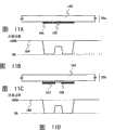
在此,参照图11A至11D说明使用多级灰度掩模59的曝光。Here, exposure using the
多级灰度掩模是可以对于曝光部分、中间曝光部分、以及未曝光部分以三种的曝光标准进行曝光的掩模,并且可以通过一次的曝光及显影工序形成具有多种(典型的是两种)厚度的区域的抗蚀剂掩模。因此,通过使用多级灰度掩模,可以缩减光掩模的数量。The multi-level grayscale mask is a mask that can be exposed with three exposure standards for the exposed part, the intermediate exposed part, and the unexposed part, and can be formed with a variety of (typically two) through one exposure and development process. species) thick regions of the resist mask. Therefore, by using a multi-tone mask, the number of photomasks can be reduced.
作为多级灰度掩模的典型例子,具有图11A所示的灰色色调掩模59a、图11C所示的半色调掩模59b。Typical examples of the multi-tone mask include a
如图11A所示,灰色色调掩模59a由具有透光性的衬底163、形成在其上的遮光部164、以及衍射光栅165构成。在遮光部164中,光的透过量为0%。另一方面,衍射光栅165通过将槽缝、点、网孔等光透过部的间隔成为用于曝光的光的分辨率限制以下的间隔来可以控制光的透过量。注意,衍射光栅165都可以使用周期性的槽缝、点、网孔、或非周期性的槽缝、点、网孔。As shown in FIG. 11A , the gray tone mask 59 a is composed of a light-transmitting
具有透光性的衬底163可以使用石英等的具有透光性的衬底。遮光部164及衍射光栅165可以使用铬、氧化铬等的吸收光的遮光材料形成。A light-transmitting substrate such as quartz can be used as the light-transmitting
在对灰色色调掩模59a照射曝光光线的情况下,如图11B所示,遮光部164中的光透过量166为0%,而不设置有遮光部164及衍射光栅165的区域中的光透过量166为100%。此外,在衍射光栅165中,可以在10%至70%的范围内调节光透过量166。通过调节衍射光栅165的槽缝、点、或网孔的间隔或间距,可以调节衍射光栅165中的光透过量。When the
如图11C所示,半色调掩模59b由具有透光性的衬底163及形成在其上的半透过部167以及遮光部168构成。半透过部167可以使用MoSiN、MoSi、MoSiO、MoSiON、CrSi等。遮光部168可以使用铬、氧化铬等的吸收光的遮光材料形成。As shown in FIG. 11C , the
在对半色调掩模59b照射曝光光线的情况下,如图11D所示,遮光部168中的光透过量169为0%,而不设置有遮光部168及半透过部167的区域中的光透过量169为100%。此外,在半透过部167中,可以在10%至70%的范围内调节光透过量169。通过调节半透过部167的材料,可以调节半透过部167中的光透过量。When the exposure light is irradiated to the
在使用多级灰度掩模曝光之后,通过进行显影,可以如图1B所示那样地形成具有膜厚度不同的区域的抗蚀剂掩模81。After exposure using a grayscale mask, development is performed to form a resist
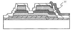
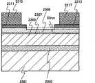
接着,通过使用抗蚀剂掩模81,蚀刻微晶半导体膜53、缓冲层54、添加有赋予一导电型的杂质元素的半导体膜55、以及导电膜65a至65c来进行分离。结果,可以形成如图2A所示那样的微晶半导体膜61、缓冲层62、添加有赋予一导电型的杂质元素的半导体膜63、以及导电膜85a至85c。注意,图2A相当于沿着图5A的A-B线的截面图(但是抗蚀剂掩模86除外)。Next, separation is performed by using the resist
通过微晶半导体膜61、缓冲层62的端部侧面倾斜,可以防止形成在缓冲层62上的源区域及漏区域和微晶半导体膜61之间产生的漏电流。此外,还可以防止源电极及漏电极和微晶半导体膜61之间产生的漏电流。微晶半导体膜61及缓冲层62的端部侧面的倾斜角度为30°至90°,优选为45°至80°。通过以这种角度形成,可以防止台阶状所引起的源电极或漏电极的断开。The inclination of the end side surfaces of the
接着,对抗蚀剂掩模81进行灰化处理。结果,抗蚀剂的面积缩小,而厚度减薄。此时,膜厚度薄的区域的抗蚀剂(与栅电极51的一部分重叠的区域)被去除,可以如图2A所示那样地形成被分离的抗蚀剂掩模86。Next, ashing treatment is performed on the resist
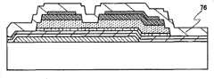
接着,使用抗蚀剂掩模86蚀刻添加有赋予一导电型的杂质元素的半导体膜63、以及导电膜85a至85c并使它们分离。在此,通过干蚀刻分离导电膜85a至85c。结果,可以形成如图2B所示那样的一对导电膜89a至89c、以及一对源区域及漏区域89。注意,在该蚀刻工序中,还蚀刻缓冲层62的一部分。将其一部分被蚀刻的缓冲层示出为缓冲层88。可以通过与形成源区域及漏区域相同的工序形成缓冲层的凹部。在此,因为缓冲层88的一部分被其面积缩小了的抗蚀剂掩模86蚀刻,所以缓冲层88突出在导电层85a至85c的外侧。Next, the
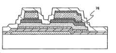
接着,如图2C所示,蚀刻导电膜89a至89c的一部分形成源电极及漏电极92a至92c。在此,当使用抗蚀剂掩模86对导电膜89a至89c湿蚀刻时,导电膜89a至89c的端部选择性地被蚀刻。结果,可以形成其面积比抗蚀剂掩模86及导电膜89a至89c小的源电极及漏电极92a至92c。源电极92a至92c的端部和源区域及漏区域89的端部不一致而偏离,即在源电极及漏电极92a至92c的端部的外侧形成源区域及漏区域89的端部。然后,去除抗蚀剂掩模86。Next, as shown in FIG. 2C, part of the
注意,图2C相当于沿着图5B的A-B线的截面图。参照图5B就知道源区域及漏区域89的端部位于源电极及漏电极92c的端部的外侧。此外缓冲层88的端部位于源电极及漏电极92c以及源区域及漏区域89的端部的外侧。此外,源电极及漏电极的一方具有部分地围绕源区域及漏区域的另一方的形状(具体而言,U字型、C字型)。由此,可以增加载流子移动的区域的面积和电流量,以可以缩小薄膜晶体管的面积。另外,因为在栅电极的内侧重叠微晶半导体膜87和源电极及漏电极92c,所以在栅电极的端部产生的凹凸的影响少。从而可以抑制覆盖率的降低和漏电流的产生。注意,源电极或漏电极的一方也起到源布线或漏布线的作用。Note that FIG. 2C corresponds to a cross-sectional view along line A-B of FIG. 5B. Referring to FIG. 5B , it can be seen that the ends of the source and drain
如图2C所示,由于通过将源电极及漏电极92a至92c的端部和源区域及漏区域89的端部形成为不一致而偏离,使源电极及漏电极92a至92c的端部的距离远离,因此可以防止源电极及漏电极之间的漏电流和短路。由此,可以制造可靠性高且耐压性高的薄膜晶体管。As shown in FIG. 2C, since the ends of the source and
通过上述工序,可以形成沟道蚀刻型薄膜晶体管83。此外,可以使用两个光掩模形成薄膜晶体管。Through the above steps, the channel-etched
在本实施方式所示的薄膜晶体管中,在栅电极上层叠有栅极绝缘膜、微晶半导体膜、缓冲层、源区域及漏区域、源电极及漏电极,并且缓冲层覆盖用作沟道形成区域的微晶半导体膜的表面。此外,在缓冲层的一部分中形成有凹部(沟槽),该凹部以外的区域被源区域及漏区域覆盖。就是说,由于源区域及漏区域之间的载流子移动的距离因形成在缓冲层的凹部而变长,因此可以减少源区域及漏区域之间的漏电流。此外,因为通过蚀刻缓冲层的一部分形成凹部,所以可以去除在源区域及漏区域的形成工序中产生的蚀刻残渣。从而可以避免在源区域及漏区域中介于残渣而产生漏电流(寄生沟道)。In the thin film transistor described in this embodiment mode, a gate insulating film, a microcrystalline semiconductor film, a buffer layer, a source region and a drain region, a source electrode and a drain electrode are stacked on the gate electrode, and the buffer layer covers the gate electrode used as the channel. The surface of the microcrystalline semiconductor film forming the region. In addition, a concave portion (trench) is formed in a part of the buffer layer, and the region other than the concave portion is covered with the source region and the drain region. That is, since the distance that carriers move between the source region and the drain region becomes longer due to the concave portion formed in the buffer layer, leakage current between the source region and the drain region can be reduced. In addition, since the concave portion is formed by etching a part of the buffer layer, it is possible to remove the etching residue generated in the process of forming the source region and the drain region. Therefore, leakage current (parasitic channel) generated by residues in the source region and the drain region can be avoided.
另外,在用作沟道形成区域的微晶半导体膜和源区域及漏区域之间形成有缓冲层。此外,微晶半导体膜的表面被缓冲层覆盖。由于使用高电阻的非晶半导体膜形成的缓冲层延伸到微晶半导体膜和源区域及漏区域之间,可以减少在薄膜晶体管截止的情况(即,对栅电极施加负电压的情况)下产生的漏电流和通过施加高电压而发生的退化。另外,因为在微晶半导体膜的表面上形成有由氢终结表面的非晶半导体膜作为缓冲层,所以可以防止微晶半导体膜的氧化,并可以在源区域及漏区域的形成工序中产生的蚀刻残渣混入到微晶半导体膜中。由此,成为电特性高且漏耐压性优良的薄膜晶体管。In addition, a buffer layer is formed between the microcrystalline semiconductor film serving as a channel formation region and the source and drain regions. In addition, the surface of the microcrystalline semiconductor film is covered with a buffer layer. Since the buffer layer formed using a high-resistance amorphous semiconductor film extends between the microcrystalline semiconductor film and the source region and the drain region, it is possible to reduce the generation of the thin film transistor when it is turned off (that is, when a negative voltage is applied to the gate electrode). leakage current and degradation by applying high voltage. In addition, since the amorphous semiconductor film whose surface is terminated by hydrogen is formed as a buffer layer on the surface of the microcrystalline semiconductor film, oxidation of the microcrystalline semiconductor film can be prevented, and problems occurring in the formation process of the source region and the drain region can be prevented. Etching residues are mixed into the microcrystalline semiconductor film. As a result, a thin film transistor having high electrical characteristics and excellent drain withstand voltage is obtained.
此外,通过将源电极及漏电极的端部和源区域及漏区域的端部形成为不一致而偏离,使源电极及漏电极的端部的距离远离,从而可以防止源电极及漏电极之间的漏电流和短路。In addition, by forming the ends of the source electrode and the drain electrode and the ends of the source region and the drain region so as to deviate from each other, the distance between the ends of the source electrode and the drain electrode is increased, thereby preventing a gap between the source electrode and the drain electrode. leakage current and short circuit.
接着,如图3A所示,在源电极及漏电极92a至92c、源区域及漏区域89、缓冲层88、微晶半导体膜87、以及栅极绝缘膜52b上形成绝缘膜76。绝缘膜76可以与栅极绝缘膜52a、52b同样地形成。注意,绝缘膜76用来防止悬浮在大气中的有机物及金属物、水蒸气等的污染杂质的侵入,优选为致密的膜。此外,通过将氮化硅膜用作绝缘膜76,缓冲层88中的氧浓度可以为5×10¹⁹atoms/cm3以下,并优选为1×1019atoms/cm3以下。Next, as shown in FIG. 3A, an insulating
接着,在绝缘膜76中形成接触孔,然后在该接触孔中形成与源电极或漏电极92c接触的像素电极77。注意,图3B相当于沿着图5C的A-B线的截面图。Next, a contact hole is formed in the insulating
作为像素电极77,可以使用具有透光性的导电材料诸如包含氧化钨的氧化铟、包含氧化钨的氧化铟锌、包含氧化钛的氧化铟、包含氧化钛的氧化铟锡、氧化铟锡(下面,称为ITO)、氧化铟锌、添加有氧化硅的氧化铟锡等。As the
另外,可以使用包含导电高分子(也称为导电聚合体)的导电组成物来形成像素电极77。在使用导电组成物形成的像素电极优选具有如下条件:薄层电阻为10000Ω/口以下,当波长为550nm时的透光率为70%以上。此外,包含在导电组成物中的导电高分子的电阻率优选为0.1Ω·cm以下。In addition, the
作为导电高分子,可以使用所谓的π电子共轭类导电高分子。例如,可以举出聚苯胺或其衍生物、聚吡咯或其衍生物、聚噻吩或其衍生物、或者由上述物质中的两种以上而成的共聚体等。As the conductive polymer, a so-called π-electron conjugated conductive polymer can be used. For example, polyaniline or its derivatives, polypyrrole or its derivatives, polythiophene or its derivatives, or the copolymer which consists of two or more of these substances etc. are mentioned.
通过上述步骤,可以形成可使用于发光装置的元件衬底。Through the above steps, an element substrate usable in a light emitting device can be formed.
注意,如图2A所示,在形成微晶半导体膜61、缓冲层62、添加有赋予一导电型的杂质元素的半导体膜63、以及导电膜85a至85c之后,如图4A所示,使用抗蚀剂掩模86蚀刻导电膜85a至85c。在此,通过使用抗蚀剂掩模86并采用湿蚀刻来各向同性地蚀刻,导电膜85a至85c的露出部及其附近选择性地被蚀刻。结果,可以形成其面积与抗蚀剂掩模86小的源电极及漏电极92a至92c。Note that, as shown in FIG. 2A, after forming the
接着,如图4B所示,使用抗蚀剂掩模86蚀刻添加有赋予一导电型的杂质元素的半导体膜63。在此,通过以干蚀刻各向异性地蚀刻添加有赋予一导电型的杂质元素的半导体膜63,可以形成其面积与抗蚀剂掩模86大致相同的源区域及漏区域89。Next, as shown in FIG. 4B , the
由于通过将源电极及漏电极92a至92c的端部和源区域及漏区域89的端部形成为不一致而偏离,使源电极及漏电极92a至92c的端部的距离远离,因此可以防止源电极及漏电极之间的漏电流和短路。由此,可以制造可靠性高且耐压性高的薄膜晶体管。Since the ends of the source and
图1A至图4B所示,通过采用湿蚀刻对导电膜进行蚀刻并采用干蚀刻对添加有赋予一导电型的杂质元素的半导体膜进行蚀刻,可以以少量的光掩模将源电极及漏电极的端部和源区域及漏区域的端部构成为不一致而不同。As shown in FIGS. 1A to 4B, by etching the conductive film by wet etching and etching the semiconductor film to which an impurity element imparting one conductivity type is added by dry etching, the source electrode and the drain electrode can be formed with a small amount of photomask. The end of the source region and the end of the drain region are configured differently and inconsistently.
接着,对于与上述方式不同的薄膜晶体管的制造方法,参照图6A至图9D进行说明。在此,下面示出源电极或漏电极和源布线或漏布线互不相同的结构。Next, a method of manufacturing a thin film transistor different from the one described above will be described with reference to FIGS. 6A to 9D . Here, the structure in which the source electrode or the drain electrode and the source wiring or the drain wiring are different from each other is shown below.
如图6A所示,在衬底50上形成栅电极51。其次,在栅电极51上按顺序形成栅极绝缘膜52a、52b、微晶半导体膜53、缓冲层54、添加有赋予一导电型的杂质元素的半导体膜55、以及导电膜65a。接着,在导电膜65a上涂敷抗蚀剂,使用图1A所示的多级灰度掩模形成具有厚度不同的区域的抗蚀剂掩模81。As shown in FIG. 6A , a
接着,使用抗蚀剂掩模81蚀刻微晶半导体膜53、缓冲层54、添加有赋予一导电型的杂质元素的半导体膜55、以及导电膜65a以进行分离。结果,可以形成如图6B所示那样的微晶半导体膜61、缓冲层62、添加有赋予一导电型的杂质元素的半导体膜63、以及导电膜85a。注意,图6B相当于沿着图9A的A-B线的截面图(但是,抗蚀剂掩模86除外)。Next, the
接着,通过对抗蚀剂掩模81进行灰化来形成分离了的抗蚀剂掩模86。然后,使用抗蚀剂掩模86蚀刻添加有赋予一导电型的杂质元素的半导体膜63、以及导电膜85a以使它们分离。在此,通过干蚀刻分离添加有赋予一导电型的杂质元素的半导体膜63、以及导电膜85a。结果,可以形成如图6C所示那样的一对导电膜89a、以及一对源区域及漏区域88。注意,在该蚀刻工序中,缓冲层62的一部分也被蚀刻。其一部分被蚀刻的缓冲层表示为缓冲层88。在此,因为缓冲层88的一部分被其面积缩小了的抗蚀剂掩模86蚀刻,所以缓冲层88突出在导电层89a的外侧。由于如本实施方式所示,缓冲层的侧面成为阶梯形状,因此后面形成的绝缘膜的覆盖率提高。由此,可以减少薄膜晶体管和形成在绝缘膜上的像素电极之间产生的漏电流。Next, the resist
接着,对抗蚀剂掩模86进行灰化。结果,如图7A所示,抗蚀剂掩模的面积缩小,且其厚度变薄。然后,通过使用被灰化的抗蚀剂掩模91蚀刻导电膜89a的一部分,如图7B所示那样地形成源电极及漏电极92a。源电极及漏电极92a的端部和源区域及漏区域89的端部不一致而偏离。在此,使用抗蚀剂掩模91并采用干蚀刻来各向异性地蚀刻导电膜89a的露出部。之后,去除抗蚀剂掩模91。Next, the resist
结果,形成与导电膜89a的面积小的源电极及漏电极92a。然后,去除抗蚀剂掩模91。注意,图7B相当于沿着图9B的A-B线的截面图。参照图9B就知道源区域及漏区域89的端部位于源电极及漏电极92a的端部的外侧。此外,缓冲层88的端部位于源电极及漏电极92a、以及源区域及漏区域89的外侧。此外,源电极及漏电极92a分别被分离,并不与形成在相邻的像素中的电极接触。注意,虽然在此使用对抗蚀剂掩模86灰化形成的抗蚀剂掩模91形成源电极及漏电极92a,但是,如图1A至图4B所示,也可以使用抗蚀剂掩模86进行湿蚀刻形成源电极及漏电极92a。As a result, the source electrode and the
如图7B所示,通过将源电极及漏电极92a的端部和源区域及漏区域89的端部形成为不一致而偏离,使源电极及漏电极92a的端部的距离远离,从而可以防止源电极及漏电极之间的漏电流和短路。由此,可以制造可靠性高且耐压性高的薄膜晶体管。As shown in FIG. 7B, by forming the ends of the source and
接着,图7C所示,在源电极及漏电极92a、源区域及漏区域89、缓冲层88、以及栅极绝缘膜52b上形成绝缘膜76。可以与栅极绝缘膜52a、52b同样地形成绝缘膜76。Next, as shown in FIG. 7C, an insulating
接着,图8A所示,在绝缘膜76中形成接触孔,并且还形成在该接触孔中与源电极及漏电极92a的一方接触并层叠的布线93b、93c。注意,图8A相当于沿着图9C的A-B线的截面图。此外,布线93a、93b是使形成在相邻的像素中的源电极或漏电极连接的布线。Next, as shown in FIG. 8A , a contact hole is formed in the insulating
接着,如图8B所示形成,在接触孔中与源电极或漏电极92a的另一方接触的像素电极77。注意,图8B相当于沿着图9D的A-B线的截面图。Next, as shown in FIG. 8B , a
通过上述工序,可以形成沟道蚀刻型薄膜晶体管84。沟道蚀刻型薄膜晶体管的制造工序少,从而可以缩减成本。此外,通过使用微晶半导体膜构成沟道形成区域,可以获得1cm2/V·sec至20cm2/V·sec的迁移率。因此,该薄膜晶体管可以用作像素部的像素的开关元件,还可以用作形成扫描线(栅极线)一侧的驱动电路的元件。Through the above steps, the channel-etched
根据本实施方式,可以制造电特性的可靠性高的薄膜晶体管。According to this embodiment mode, it is possible to manufacture a thin film transistor with high reliability in electrical characteristics.
实施方式2
下面,参照图2A至2C及图15A和15B对发光装置的制造工序进行说明。在此使用利用电致发光的发光元件来表示发光装置。根据发光材料是有机化合物还是无机化合物,对利用电致发光的发光元件进行分类。一般地,前者被称为有机EL元件,后者被称为无机EL元件。另外,在此虽然使用图1A和1B及图2A至2C示出薄膜晶体管的制造工序,但也可适当地使用图4A和4B、图6A至图8B。Next, the manufacturing process of the light emitting device will be described with reference to FIGS. 2A to 2C and FIGS. 15A and 15B. Here, a light emitting device utilizing electroluminescence is used to represent a light emitting device. Light-emitting elements utilizing electroluminescence are classified according to whether the light-emitting material is an organic compound or an inorganic compound. Generally, the former is called an organic EL element, and the latter is called an inorganic EL element. 1A and 1B and FIGS. 2A to 2C are used to illustrate the manufacturing process of the thin film transistor. However, FIGS. 4A and 4B and FIGS. 6A to 8B may be used as appropriate.
有机EL元件通过对发光元件施加电压,来自一对电极的电子及空穴分别注入到包含发光有机化合物的层中,由此电流流通。然后,通过这些载流子(电子及空穴)重组,该发光有机化合物形成激发态,并且从激发态回到基态时发光。由于这样的机理,这样的发光元件被称为电流激发型发光元件。In the organic EL element, when a voltage is applied to the light-emitting element, electrons and holes from a pair of electrodes are respectively injected into a layer containing a light-emitting organic compound, whereby a current flows. Then, by recombination of these carriers (electrons and holes), the light-emitting organic compound forms an excited state, and emits light when returning from the excited state to the ground state. Due to such a mechanism, such a light emitting element is called a current excitation type light emitting element.
无机EL元件根据其元件结构分类为分散型无机EL元件和薄膜型无机EL元件。分散型无机EL元件包括将发光材料颗粒分散在粘合剂中的发光层,并且其发光机理是利用施主能级和受主能级的施主-受主复合型发光。薄膜型无机EL元件是将发光层夹在电介质层中,并将其夹在电极中的结构,其发光机理是利用金属离子内壳层电子跃迁的局限型发光。注意,在此,使用有机EL元件作为发光元件进行说明。另外,虽然使用图2C所示的沟道蚀刻型薄膜晶体管示出用来控制发光元件的驱动的薄膜晶体管,也可适当地使用沟道保护型薄膜晶体管。Inorganic EL elements are classified into dispersion type inorganic EL elements and thin film type inorganic EL elements according to their element structures. The dispersion-type inorganic EL element includes a light-emitting layer in which particles of a light-emitting material are dispersed in a binder, and its light-emitting mechanism is a donor-acceptor recombination light emission using a donor level and an acceptor level. The thin-film inorganic EL element is a structure in which the light-emitting layer is sandwiched between the dielectric layer and the electrode, and its light-emitting mechanism is a confined light emission using the electronic transition of the inner shell of metal ions. Note that, here, an organic EL element is used as a light-emitting element for description. In addition, although the thin film transistor used to control the driving of the light emitting element is shown using the channel etching type thin film transistor shown in FIG. 2C , a channel protecting type thin film transistor may be suitably used.
经过图1A和1B及图2A至2C的工序,如图15A和15B所示,在衬底50上形成薄膜晶体管83以及85,在薄膜晶体管83上形成用作保护膜的绝缘膜76。注意,薄膜晶体管85是形成在驱动电路121中的,而薄膜晶体管83是形成在像素部122中的。接着,在绝缘膜76上形成平坦化膜111,并在平坦化膜111上形成与薄膜晶体管83的源电极或漏电极连接的像素电极112。1A and 1B and 2A to 2C, as shown in FIGS. 15A and 15B,
平坦化膜111优选由丙烯、聚酰亚胺、聚酰胺等的有机树脂或者硅氧烷形成。The
在图15A中,由于像素的薄膜晶体管是n型,所以优选将像素电极112用作阴极,但是相反的,如果像素的薄膜晶体管是p型的情况下则优选用作阳极。具体地说,可以使用已知的功函数小的材料如Ca、Al、CaF、MgAg、AlLi等作为阴极。In FIG. 15A, since the thin film transistor of the pixel is n-type, the
接着,如图15B所示,在平坦化膜111及像素电极112的端部上形成分隔壁113。分隔壁113具有开口部,在该开口部中,像素电极112露出。分隔壁113使用有机树脂膜、无机绝缘膜或有机聚硅氧烷形成。特别是,优选使用感光材料,在像素电极上形成开口部,并以该开口部的侧壁成为具有连续曲率形成的倾斜面的方式形成分隔壁113。Next, as shown in FIG. 15B ,
接着,以在分隔壁113的开口部中与像素电极112接触的方式形成发光层114。发光层114既可以由单层构成,又可以由多个层的叠层构成。Next, the
而且,覆盖发光层114地形成使用阳极材料的共同电极115。可以采用在实施方式1中作为像素电极77举出的使用具有透光性的导电材料的透光导电膜来形成共同电极115。作为共同电极115,除了上述透光导电膜之外,还可以使用氮化钛膜或钛膜。在图15B中,使用ITO作为共同电极115。在分隔壁113的开口部中,通过像素电极112、发光层114以及共同电极115彼此重叠,形成发光元件117。然后,优选在共同电极115及分隔壁113上形成保护膜116,以免氧、氢、水分、二氧化碳等侵入到发光元件117中。作为保护膜116,可以形成氮化硅膜、氮氧化硅膜、DLC膜等。Furthermore, a
再者,实际上,在图15B的步骤之后,优选使用气密性高且漏气少的保护薄膜(层压薄膜、紫外线固化树脂薄膜等)及覆盖材料封装(密封),以免露出到外气。Furthermore, in fact, after the step of FIG. 15B, it is preferable to use a protective film (lamination film, ultraviolet curable resin film, etc.) with high airtightness and little air leakage and a covering material to encapsulate (seal) so as not to expose to the outside air. .
接着,参照图16A至16C说明发光元件的结构。在此,作为例子举出驱动TFT是n型的情况来说明像素的截面结构。Next, the structure of the light emitting element will be described with reference to FIGS. 16A to 16C. Here, the cross-sectional structure of a pixel will be described by taking a case where the driving TFT is an n-type as an example.
在发光元件中,为取出光而阳极及阴极的至少一方是透明,即可。而且,作为发光元件,具有在衬底上形成薄膜晶体管及发光元件且从与衬底相反一侧取出光的顶部发射结构、从衬底一侧取出光的底部发射结构、从与衬底一侧以及衬底相反一侧的面取出光的双面发射结构。本发明的像素结构可以应用于任何发射结构的发光元件。In the light-emitting element, at least one of the anode and the cathode may be transparent in order to extract light. Furthermore, as a light-emitting element, there are a top emission structure in which a thin film transistor and a light-emitting element are formed on a substrate and takes out light from the side opposite to the substrate, a bottom emission structure in which light is taken out from the substrate side, and a bottom emission structure in which light is taken out from the side of the substrate. And a double-sided emission structure that extracts light from the surface on the opposite side of the substrate. The pixel structure of the present invention can be applied to light-emitting elements of any emission structure.
对于顶部发射结构的发光元件,参照图16A来说明。A light-emitting element with a top emission structure will be described with reference to FIG. 16A .
图16A示出一种像素的截面图,其中驱动TFT7001是n型,且从发光元件7002发射的光穿过到阳极7005一侧。在图16A中,发光元件7002的阴极7003和驱动TFT7001电连接,并且在阴极7003上按顺序层叠发光层7004和阳极7005。阴极7003只要是功函数小且反射光的导电膜的导电膜,而可以使用已知的材料。例如,优选使用Ca、Al、CaF、MgAg、AlLi等。此外,发光层7004既可以由单层构成,又可以多个层构成。在由多个层构成的情况下,在阴极7003上按顺序层叠电子注入层、电子传输层、发光层、空穴传输层、以及空穴注入层。注意,不需要设置这种层的全部。阳极7005使用透过光的具有透光性的导电材料形成,例如,可以使用具有透光性的导电膜诸如包含氧化钨的氧化铟、包含氧化钨的氧化铟锌、包含氧化钛的氧化铟、包含氧化钛的氧化铟锡、氧化铟锡(下面,称为ITO)、氧化铟锌、添加有氧化硅的氧化锡等。FIG. 16A shows a cross-sectional view of a pixel in which a driving
由阴极7003以及阳极7005夹着发光层7004的区域相当于发光元件7002。在图16A所示的像素中,从发光元件7002发射的光如空心箭头所示那样发射到阳极7005一侧。The region where the light-emitting
接着,参照图16B来说明底部发射结构的发光元件。图16B示出一种像素的截面图,其中驱动TFT7011是n型,从发光元件7012发射的光发射到阴极7013一侧。在图16B中,在与驱动TFT7011电连接的具有透光性的导电材料7017上形成了发光元件7012的阴极7013,而在阴极7013上按顺序层叠发光层7014、阳极7015。注意,在阳极7015具有透光性的情况下,也可以以覆盖阳极上的方式形成用来反射光或屏蔽光的屏蔽膜7016。与图16A的情况相同,只要是功函数小的导电膜而可以使用已知的材料作为阴极7013。但是,其膜厚度为透过光的程度(优选为5nm至30nm左右)。例如,可以将具有20nm的膜厚度的Al用作阴极7013。而且,与图16A的情况相同,发光层7014既可以由单层构成,又可以由多个层构成。阳极7015不需要透过光,但是可以与图16A的情况相同地使用具有透光性的导电材料形成。而且,例如可以使用反射光的金属等作为屏蔽膜7016,然而不局限于金属膜。比如说,也可以使用添加有黑颜料的树脂等。Next, a light emitting element having a bottom emission structure will be described with reference to FIG. 16B . 16B shows a cross-sectional view of a pixel in which the driving
由阴极7013及阳极7015夹着发光层7014的区域相当于发光元件7012。在图16B所示的像素中,从发光元件7012发射的光如空心箭头所示那样发射到阴极7013一侧。The region where the light-emitting
接着,参照图16C来说明双面发射结构的发光元件。在图16C中,与驱动TFT7021电连接的具有透光性的导电材料7027上形成发光元件7022的阴极7023,在阴极7023上按顺序层叠有发光层7024、阳极7025。与图16A的情况相同,阴极7023只要是功函数小的导电膜,而可以使用已知的材料。但是,其膜厚度为透过光的程度。例如,可以将具有20nm的膜厚度的Al用作阴极7023。而且,与图16A的情况相同,发光层7024既可以由单层构成,又可以多个层的叠层构成。阳极7025可以与图16A的情况相同地使用具有透光性的导电材料形成。Next, a light-emitting element with a double-sided emission structure will be described with reference to FIG. 16C . In FIG. 16C , a
阴极7023、发光层7024、阳极7025重叠的部分相当于发光元件7022。在图16C所示的像素中,从发光元件7022发射的光如空心箭头所示那样发射到阳极7025一侧和阴极7023一侧。The portion where the
注意,在此描述有机EL元件作为发光元件,但是也可以设置无机EL元件作为发光元件。Note that an organic EL element is described here as a light emitting element, but an inorganic EL element may also be provided as a light emitting element.
注意,在本实施方式中,示出了控制发光元件的驱动的薄膜晶体管(驱动TFT)和发光元件彼此电连接的例子,但是也可以采用电流控制TFT连接到驱动TFT和发光元件之间的结构。Note that in this embodiment mode, an example in which a thin film transistor (driving TFT) for controlling the driving of the light emitting element and the light emitting element are electrically connected to each other is shown, but a structure in which a current control TFT is connected between the driving TFT and the light emitting element may also be employed. .
注意,本实施方式所示的发光装置不局限于图16A至16C所示的结构,而可以根据本发明的技术想法改变为各种方式。Note that the light emitting device shown in this embodiment mode is not limited to the structure shown in FIGS. 16A to 16C , but can be changed in various ways according to the technical idea of the present invention.
通过上述工序,可以制造发光装置。由于本实施方式的发光装置使用截止电流少且电特性的可靠性高的薄膜晶体管,因此成为对比度高且可见度高的发光装置。此外,因为采用没有激光晶化工序的微晶半导体膜的薄膜晶体管,所以可以批量生产性高地制造可见度高的发光装置。Through the above steps, a light emitting device can be manufactured. Since the light-emitting device of this embodiment uses a thin film transistor with a small off-state current and high reliability of electrical characteristics, it is a light-emitting device with high contrast and high visibility. In addition, since a thin-film transistor of a microcrystalline semiconductor film without a laser crystallization process is used, a high-visibility light-emitting device can be manufactured with high mass productivity.
实施方式3Embodiment 3
接着,下面示出本发明的发光装置的一个方式的发光面板结构。Next, the light emitting panel structure of one embodiment of the light emitting device of the present invention is shown below.
图12A示出一种发光面板的方式,其中另行形成信号线驱动电路6013且将该信号线驱动电路6013与形成在衬底6011上的像素部6012连接。像素部6012及扫描线驱动电路6014采用将微晶半导体膜用于沟道形成区域的薄膜晶体管形成。通过采用可获得比将微晶半导体膜用于沟道形成区域的薄膜晶体管高的电场效应迁移率的晶体管形成信号线驱动电路,可以使被要求比扫描线驱动电路高的驱动频率的信号线驱动电路的工作稳定。注意,信号线驱动电路6013也可以是将单晶半导体用于沟道形成区域的晶体管、将多晶半导体用于沟道形成区域的薄膜晶体管、或使用SOI的晶体管。对于像素部6012、信号线驱动电路6013、扫描线驱动电路6014分别通过FPC6015供给电源电位、各种信号等。FIG. 12A shows a form of a light-emitting panel in which a signal
此外,信号线驱动电路及扫描线驱动电路也可以一起形成在与像素部相同的衬底上。In addition, the signal line driver circuit and the scan line driver circuit may be formed together on the same substrate as the pixel portion.
另外,在另行形成驱动电路的情况下,不一定需要将形成有驱动电路的衬底贴附在形成有像素部的衬底上,例如也可以贴附在FPC上。图12B示出一种发光装置面板的方式,其中另行形成信号线驱动电路6023,且将形成在衬底6021上的像素部6022和信号线驱动电路6023彼此连接。像素部6022及扫描线驱动电路6024采用将微晶半导体膜用于沟道形成区域的薄膜晶体管形成。信号线驱动电路6023通过FPC6025与像素部6022连接。对于像素部6022、信号线驱动电路6023、扫描线驱动电路6024分别通过FPC6025供给电源电位、各种信号等。In addition, when the driver circuit is formed separately, the substrate on which the driver circuit is formed does not necessarily have to be attached to the substrate on which the pixel portion is formed, and may be attached to an FPC, for example. 12B shows a form of a light-emitting device panel in which a signal
此外,也可以采用将微晶半导体膜用于沟道形成区域的薄膜晶体管只将信号线驱动电路的一部分或扫描线驱动电路的一部分形成在与像素部相同的衬底上,并且另行形成其他部分并使它电连接到像素部。图12C示出一种发光装置面板的方式,将信号线驱动电路所具有的模拟开关6033a形成在与像素部6032、扫描线驱动电路6034相同的衬底6031上,并且将信号线驱动电路所具有的移位寄存器6033b另行形成在不同的衬底上并彼此贴合。像素部6032及扫描线驱动电路6034采用将微晶半导体膜用于沟道形成区域的薄膜晶体管形成。信号线驱动电路所具有的移位寄存器6033b通过FPC6035与像素部6032连接。对于像素部6032、信号线驱动电路、扫描线驱动电路6034分别通过FPC6035供给电源电位、各种信号等。In addition, it is also possible to use a thin film transistor using a microcrystalline semiconductor film as a channel formation region, forming only a part of the signal line driver circuit or a part of the scanning line driver circuit on the same substrate as the pixel portion, and forming other parts separately. And make it electrically connected to the pixel portion. 12C shows a method of a light-emitting device panel. The
如图12A至12C所示,在本发明的发光装置中,可以采用将微晶半导体膜用于沟道形成区域的薄膜晶体管将驱动电路的一部分或全部形成在与像素部相同的衬底上。As shown in FIGS. 12A to 12C, in the light-emitting device of the present invention, part or all of the driver circuit can be formed on the same substrate as the pixel portion using a thin film transistor using a microcrystalline semiconductor film for the channel formation region.
注意,对于另行形成的衬底的连接方法没有特别的限制,可以采用已知的COG方法、引线键合方法、或TAB方法等。此外,若是能够电连接,连接位置不局限于图12A至12C所示的位置。另外,也可以另行形成控制器、CPU、存储器等而连接。Note that there is no particular limitation on the connection method of the separately formed substrates, and a known COG method, a wire bonding method, or a TAB method, etc. may be employed. In addition, the connection positions are not limited to those shown in FIGS. 12A to 12C if they can be electrically connected. In addition, a controller, a CPU, a memory, and the like may be separately formed and connected.
注意,用于本发明的信号线驱动电路不局限于只有移位寄存器和模拟开关的方式。除了移位寄存器和模拟开关之外,也可以具有其他电路如缓冲器、电平转移器、源极跟随器等。此外,不一定设置移位寄存器和模拟开关,例如既可以使用如译码器电路的能够选择信号线的其他电路代替移位寄存器,又可以使用锁存器等代替模拟开关。Note that the signal line driver circuit used in the present invention is not limited to only shift registers and analog switches. In addition to shift registers and analog switches, there may also be other circuits such as buffers, level shifters, source followers, etc. In addition, it is not necessary to provide a shift register and an analog switch. For example, a circuit such as a decoder circuit capable of selecting a signal line may be used instead of the shift register, or a latch or the like may be used instead of the analog switch.
图18示出本发明的发光装置的框图。图18所示的发光装置包括具有多个具备发光元件的像素的像素部700、选择各个像素的扫描线驱动电路702、控制对被选择的像素的视频信号的输入的信号线驱动电路703。Fig. 18 shows a block diagram of a light emitting device of the present invention. The light emitting device shown in FIG. 18 includes a pixel unit 700 having a plurality of pixels including light emitting elements, a scanning
在图18中,信号线驱动电路703包括移位寄存器704和模拟开关705。时钟信号(CLK)、起始脉冲信号(SP)输入到移位寄存器704中。当时钟信号(CLK)和起始脉冲信号(SP)被输入时,在移位寄存器704中产生时序信号,并输入到模拟开关705。In FIG. 18 , a signal
此外,模拟开关705提供有视频信号。模拟开关705根据被输入的时序信号对视频信号进行取样,然后供给给后级的信号线。Also, the
接着,说明扫描线驱动电路702的结构。扫描线驱动电路702包括移位寄存器706、缓冲器707。此外,也可以根据情况包括电平转移器。在扫描线驱动电路702的移位寄存器706中,通过时钟信号(CLK)及起始脉冲信号(SP)被输入,产生选择信号。产生了的选择信号在缓冲器707中被缓冲放大,并被供给到对应的扫描线。一个像素的晶体管的栅极连接到扫描线。而且,由于需要使一条线上的像素的晶体管同时导通,因此使用能够流过大电流的缓冲器707。Next, the configuration of the scanning
在全彩色发光装置中,在将对应于R(红)、G(绿)、B(蓝)的视频信号按顺序进行取样而供给给对应的信号线的情况下,用来连接移位寄存器704和模拟开关705的端子数相当于用来连接模拟开关705和像素部700的信号线的端子数的1/3左右。因此,通过将模拟开关705形成在与像素部700相同的衬底上,与将模拟开关705形成在与像素部700不同的衬底上时相比,可以减少用来连接另行形成的衬底的端子数,并且抑制连接不良的发生比率,以可以提高成品率。In a full-color light-emitting device, when video signals corresponding to R (red), G (green), and B (blue) are sequentially sampled and supplied to corresponding signal lines, it is used to connect the
此外,图18的扫描线驱动电路702包括移位寄存器706、及缓冲器707,但是也可以由移位寄存器706构成扫描线驱动电路702。In addition, the scanning
注意,图18所示的结构只是本发明的发光装置的一个方式,信号线驱动电路和扫描线驱动电路的结构不局限于此。Note that the structure shown in FIG. 18 is only one form of the light-emitting device of the present invention, and the structures of the signal line driver circuit and the scan line driver circuit are not limited thereto.
接着,参照图19及图20说明包括将极性都相同的微晶半导体膜用于沟道形成区域的薄膜晶体管的移位寄存器的一个方式。图19示出本实施方式的移位寄存器的结构。图19所示的移位寄存器由多个触发器(触发器701-1至701-n)构成。此外,被输入第一时钟信号、第二时钟信号、起始脉冲信号、复位信号而工作。Next, an embodiment of a shift register including a thin film transistor using a microcrystalline semiconductor film having the same polarity for a channel formation region will be described with reference to FIGS. 19 and 20 . FIG. 19 shows the structure of the shift register of this embodiment. The shift register shown in FIG. 19 is composed of a plurality of flip-flops (flip-flops 701-1 to 701-n). In addition, the first clock signal, the second clock signal, the start pulse signal, and the reset signal are input to operate.
说明图19的移位寄存器的连接关系。在图19的移位寄存器的第i级的触发器701-i(触发器701-1至701-n中任何一个)中,图20所示的第一布线501连接到第七布线717-i-1,图20所示的第二布线502连接到第七布线717-i+1,图20所示的第三布线503连接到第七布线717-i,图20所示的第六布线506连接到第五布线715。The connection relation of the shift register in Fig. 19 will be described. In the flip-flop 701-i (any one of the flip-flops 701-1 to 701-n) of the i-th stage of the shift register of FIG. 19 , the
此外,图20所示的第四布线504在第奇数级的触发器中连接到第二布线712,在第偶数级的触发器中连接到第三布线713,图20所示的第五布线505连接到第四布线714。In addition, the
但是,第一级的触发器701-1中的图20所示的第一布线501连接到第一布线71 1,第n级的触发器701-n的图20所示的第二布线502连接到第六布线716。However, the
注意,第一布线711、第二布线712、第三布线713、第六布线716也可以分别称为第一信号线、第二信号线、第三信号线、第四信号线。再者,第四布线714、第五布线715也可以分别称为第一电源线、第二电源线。Note that the
接着,图20示出图19所示的触发器的详细结构。图20所示的触发器包括第一薄膜晶体管171、第二薄膜晶体管172、第三薄膜晶体管173、第四薄膜晶体管174、第五薄膜晶体管175、第六薄膜晶体管176、第七薄膜晶体管177、以及第八薄膜晶体管178。在本实施方式中,第一薄膜晶体管171、第二薄膜晶体管172、第三薄膜晶体管173、第四薄膜晶体管174、第五薄膜晶体管175、第六薄膜晶体管176、第七薄膜晶体管177、以及第八薄膜晶体管178是n型沟道晶体管,并且当栅极-漏极之间的电压(Vgs)大于阈值电压(Vth)时其处于导通状态。Next, FIG. 20 shows a detailed structure of the flip-flop shown in FIG. 19 . The trigger shown in FIG. 20 includes a first
接着,下面示出图20所示的触发器的连接结构。Next, the connection structure of the flip-flop shown in FIG. 20 is shown below.
第一薄膜晶体管171的第一电极(源电极及漏电极的一方)连接到第四布线504,第一薄膜晶体管171的第二电极(源电极及漏电极的另一方)连接到第三布线503。The first electrode (one of the source electrode and the drain electrode) of the first
第二薄膜晶体管172的第一电极连接到第六布线506,第二薄膜晶体管172的第二电极连接到第三布线503。The first electrode of the second
第三薄膜晶体管173的第一电极连接到第五布线505,第三薄膜晶体管173的第二电极连接到第二薄膜晶体管172的栅电极,第三薄膜晶体管173的栅电极连接到第五布线505。The first electrode of the third
第四薄膜晶体管174的第一电极连接到第六布线506,第四薄膜晶体管174的第二电极连接到第二薄膜晶体管172的栅电极,第四薄膜晶体管174的栅电极连接到第一薄膜晶体管171的栅电极。The first electrode of the fourth
第五薄膜晶体管175的第一电极连接到第五布线505,第五薄膜晶体管175的第二电极连接到第一薄膜晶体管171的栅电极,第五薄膜晶体管175的栅电极连接到第一布线501。The first electrode of the fifth
第六薄膜晶体管176的第一电极连接到第六布线506,第六薄膜晶体管176的第二电极连接到第一薄膜晶体管171的栅电极,第六薄膜晶体管176的栅电极连接到第二薄膜晶体管172的栅电极。The first electrode of the sixth
第七薄膜晶体管177的第一电极连接到第六布线506,第七薄膜晶体管177的第二电极连接到第一薄膜晶体管171的栅电极,第七薄膜晶体管177的栅电极连接到第二布线502。第八薄膜晶体管178的第一电极连接到第六布线506,第八薄膜晶体管178的第二电极连接到第二薄膜晶体管172的栅电极,第八薄膜晶体管178的栅电极连接到第一布线501。The first electrode of the seventh
注意,以第一薄膜晶体管171的栅电极、第四薄膜晶体管174的栅电极、第五薄膜晶体管175的第二电极、第六薄膜晶体管176的第二电极、以及第七薄膜晶体管177的第二电极的连接部分为节点143。再者,以第二薄膜晶体管172的栅电极、第三薄膜晶体管173的第二电极、第四薄膜晶体管174的第二电极、第六薄膜晶体管176的栅电极、以及第八薄膜晶体管178的第二电极的连接部分为节点144。Note that, with the gate electrode of the first
注意,第一布线501、第二布线502、第三布线503、第四布线504也可以分别称为第一信号线、第二信号线、第三信号线、第四信号线。再者,第五布线505、第六布线506也可以分别称为第一电源线、第二电源线。Note that the
图21示出图20所示的触发器的俯视图的一个例子。FIG. 21 shows an example of a top view of the trigger shown in FIG. 20 .
导电膜901包括用作第一薄膜晶体管171的第一电极的部分,并通过与像素电极同时形成的布线951与第四布线504连接。The conductive film 901 includes a portion serving as the first electrode of the first
导电膜902包括用作第一薄膜晶体管171的第二电极的部分,并通过与像素电极同时形成的布线952与第三布线503连接。The conductive film 902 includes a portion serving as the second electrode of the first
导电膜903包括用作第一薄膜晶体管171的栅电极的部分、以及第四薄膜晶体管174的用作栅电极的部分。The conductive film 903 includes a portion serving as the gate electrode of the first
导电膜904包括用作第二薄膜晶体管172的第一电极的部分、用作第六薄膜晶体管176的第一电极的部分、用作第四薄膜晶体管174的第一电极的部分、以及用作第八薄膜晶体管178的第一电极的部分,并与第六布线506连接。The conductive film 904 includes a portion serving as the first electrode of the second
导电膜905包括用作第二薄膜晶体管172的第二电极的部分,并通过与像素电极同时形成的布线954与第三布线503连接。The conductive film 905 includes a portion serving as the second electrode of the second
导电膜906包括用作第二薄膜晶体管172的栅电极的部分、以及用作第六薄膜晶体管176的栅电极的部分。The conductive film 906 includes a portion serving as the gate electrode of the second
导电膜907包括用作第三薄膜晶体管173的第一电极的部分,并通过布线955与第五布线505连接。The conductive film 907 includes a portion serving as the first electrode of the third
导电膜908包括用作第三薄膜晶体管173的第二电极的部分、以及用作第四薄膜晶体管174的第二电极的部分,并通过与像素电极同时形成的布线956与导电膜906连接。The conductive film 908 includes a portion serving as the second electrode of the third
导电膜909包括用作第三薄膜晶体管173的栅电极的部分,并通过布线955与第五布线505连接。The conductive film 909 includes a portion serving as a gate electrode of the third
导电膜910包括用作第五薄膜晶体管175的第一电极的部分,并通过与像素电极同时形成的布线959与第五布线505连接。The conductive film 910 includes a portion serving as the first electrode of the fifth
导电膜911包括用作第五薄膜晶体管175的第二电极的部分、以及用作第七薄膜晶体管177的第二电极的部分,并通过与像素电极同时形成的布线958与导电膜903连接。The conductive film 911 includes a portion serving as the second electrode of the fifth
导电膜912包括用作第五薄膜晶体管175的栅电极的部分,并通过与像素电极同时形成的布线960与第一布线501连接。The conductive film 912 includes a portion serving as a gate electrode of the fifth
导电膜913包括用作第六薄膜晶体管176的第二电极的部分,并通过与像素电极同时形成的布线957与导电膜903连接。The conductive film 913 includes a portion serving as the second electrode of the sixth
导电膜914包括用作第七薄膜晶体管177的栅电极的部分,并通过与像素电极同时形成的布线962与第二布线502连接。The conductive film 914 includes a portion serving as a gate electrode of the seventh
导电膜915包括用作第八薄膜晶体管178的栅电极的部分,并通过与像素电极同时形成的布线961与导电膜912连接。The conductive film 915 includes a portion serving as a gate electrode of the eighth
导电膜916包括第八薄膜晶体管178的用作第二电极的部分,并通过与像素电极同时形成的布线953与导电膜906连接。The conductive film 916 includes a portion serving as the second electrode of the eighth
注意,微晶半导体膜981至988的一部分分别用作第一至第八薄膜晶体管的沟道形成区域。Note that parts of the microcrystalline semiconductor films 981 to 988 serve as channel formation regions of the first to eighth thin film transistors, respectively.
注意,通过由将微晶半导体用于沟道形成区域的晶体管构成图19和图20所示的电路,可以缩小设计面积。因此,可以缩小发光装置的边框。例如,当对将非晶半导体膜用于沟道形成区域的情况和将微晶半导体膜用于沟道形成区域的情况进行比较时,将微晶半导体膜用于沟道形成区域的情况下的薄膜晶体管的电场效应迁移率较高,因此可以缩小晶体管的沟道宽度。结果,可以实现发光装置的窄边框化。作为一个例子,第二薄膜晶体管172的沟道宽度为3000μm以下,更优选为2000μm以下。Note that the design area can be reduced by configuring the circuits shown in FIGS. 19 and 20 with transistors using a microcrystalline semiconductor for the channel formation region. Therefore, the frame of the light emitting device can be reduced. For example, when comparing the case where an amorphous semiconductor film is used for a channel formation region and the case where a microcrystalline semiconductor film is used for a channel formation region, in the case where a microcrystalline semiconductor film is used for a channel formation region, the The electric field effect mobility of the thin film transistor is high, so the channel width of the transistor can be narrowed. As a result, frame narrowing of the light emitting device can be realized. As an example, the channel width of the second
注意,在图20的第二薄膜晶体管172中,对于第三布线503输出低电平的信号的期间长。其间,第二薄膜晶体管172一直处于导通状态。因此,第二薄膜晶体管172受到很强的压力,而晶体管特性容易退化。当晶体管特性退化时,阈值电压逐渐增大。结果,电流值逐渐缩小。于是,第二薄膜晶体管172的沟道宽度优选大,以便即使晶体管退化也能够供给充分的电流。或者,优选被补偿以便防止在晶体管的退化时产生的电路工作的障碍。例如,优选通过与第二薄膜晶体管172并列地配置晶体管,并使它与第二薄膜晶体管172交替处于导通状态,不容易受到退化的影响。Note that in the second
然而,当对将非晶半导体膜用于沟道形成区域的情况和将微晶半导体膜用于沟道形成区域的情况进行比较时,将微晶半导体膜用于沟道形成区域的晶体管较不容易退化。因此,在将微晶半导体膜用于沟道形成区域的情况下,可以缩小晶体管的沟道宽度。或者,即使不设置对于退化的补偿用电路也可以进行正常工作。由此,可以缩小设计面积。However, when the case of using the amorphous semiconductor film for the channel formation region and the case of using the microcrystalline semiconductor film for the channel formation region are compared, the transistor using the microcrystalline semiconductor film for the channel formation region is inferior. easy to degrade. Therefore, when the microcrystalline semiconductor film is used for the channel formation region, the channel width of the transistor can be reduced. Alternatively, normal operation can be performed without providing a circuit for compensating for degradation. Thus, the design area can be reduced.
接着,参照图17A和17B说明相当于本发明的发光装置的一个方式的发光显示面板的外观及截面。图17A是一种面板的俯视图,其中在与第二衬底之间使用密封材料密封将形成在第一衬底上的具有微晶半导体膜用作沟道形成区域的薄膜晶体管及发光元件。图17B相当于沿着图17A的A-A’线的截面图。Next, the appearance and cross-section of a light-emitting display panel corresponding to one embodiment of the light-emitting device of the present invention will be described with reference to FIGS. 17A and 17B . 17A is a plan view of a panel in which thin film transistors and light emitting elements having a microcrystalline semiconductor film serving as a channel formation region formed on a first substrate are sealed with a sealing material between the second substrate. Fig. 17B corresponds to a cross-sectional view along line A-A' of Fig. 17A.
以围绕形成在第一衬底4001上的像素部4002和扫描线驱动电路4004的方式设置有密封材料4005。此外,在像素部4002和扫描线驱动电路4004上设置第二衬底4006。因此,使用第一衬底4001、密封材料4005以及第二衬底4006将像素部4002和扫描线驱动电路4004与填充材料4007一起密封。另外,在第一衬底4001上的与由密封材料4005围绕的区域不同的区域中安装有使用多晶半导体膜形成在另行准备的衬底上的信号线驱动电路4003。注意,本实施方式说明具有将多晶半导体膜用于沟道形成区域的薄膜晶体管的信号线驱动电路贴附到第一衬底4001的例子,但是也可以采用将单晶半导体用于沟道形成区域的晶体管形成信号线驱动电路并贴合。图17A和17B例示包括在信号线驱动电路4003中的由多晶半导体膜形成的薄膜晶体管4009。A sealing
此外,设置在第一衬底4001上的像素部4002和扫描线驱动电路4004包括多个薄膜晶体管,图17B例示包括在像素部4002中的薄膜晶体管4010。注意,虽然在本实施方式中,薄膜晶体管4010假定是驱动TFT,但是薄膜晶体管4010既可以是电流控制TFT,又可以是擦除TFT。薄膜晶体管4010相当于将微晶半导体膜用于沟道形成区域的薄膜晶体管。Furthermore, the
另外,附图标记4011相当于发光元件,发光元件4011所具有的像素电极4030与薄膜晶体管4010的源电极或漏电极4017电连接。而且,在本实施方式中,发光元件4011的具有透光性的导电材料4012电连接。注意,发光元件4011的结构不局限于本实施方式所示的结构。可以根据从发光元件4011取出的光的方向、以及薄膜晶体管4010的极性而适当地改变发光元件4011的结构。In addition,
此外,虽然在图17B所示的截面图中未图示,但是提供到另行形成的信号线驱动电路4003和扫描线驱动电路4004或像素部4002的各种信号及电位通过引导布线4014以及4015从FPC4018供给。In addition, although not shown in the cross-sectional view shown in FIG. 17B , various signals and potentials supplied to the separately formed signal
在本实施方式中,连接端子4016由与发光元件4011所具有的像素电极4030相同的导电膜形成。此外,引导布线4014、4015由与布线4017相同的导电膜形成。In this embodiment, the
连接端子4016通过各向异性导电膜4019电连接到FPC4018所具有的端子。The
位于从发光元件4011取出光的方向上的衬底必须是透明的衬底。在此情况下,使用具有透光性的材料如玻璃片、塑料片、聚酯薄膜、或丙烯薄膜。The substrate located in the direction in which light is extracted from the
此外,作为填充材料4007,除了氮、氩等的惰性气体之外,还可以使用紫外线固化树脂、热固化树脂、PVC(聚氯乙烯)、丙烯、聚酰亚胺、环氧树脂、硅树脂、PVB(聚乙烯醇缩丁醛)、或EVA(乙烯-醋酸乙烯酯)。在本实施方式中,使用氮作为填充材料。In addition, as the
另外,如果需要,也可以在发光元件的发射面上适当地设置光学薄膜如偏振片、圆偏振片(椭圆偏振片)、相位差板(λ/4板、λ/2板)、或颜色滤光片等。此外,还可以在偏振片或圆偏振片上设置防反射膜。例如,可以执行抗眩光处理,该处理是利用表面的凹凸来扩散反射光并降低眩光的。In addition, if necessary, an optical film such as a polarizer, a circular polarizer (elliptical polarizer), a phase difference plate (λ/4 plate, λ/2 plate), or a color filter can also be appropriately arranged on the emitting surface of the light-emitting element. light sheet etc. In addition, an antireflection film may be provided on the polarizing plate or the circular polarizing plate. For example, anti-glare treatment can be performed, which uses the unevenness of the surface to diffuse reflected light and reduce glare.
注意,图17A和17B示出另行形成信号线驱动电路4003而安装到第一衬底4001的例子,但是本实施方式不局限于此。既可以另行形成扫描线驱动电路而安装,又可以另行形成信号线驱动电路的一部分或扫描线驱动电路的一部分而安装。Note that FIGS. 17A and 17B show an example in which the signal
本实施方式可以与其他实施方式所记载的结构组合而实施。This embodiment mode can be implemented in combination with the structures described in other embodiment modes.
实施方式4Embodiment 4
通过采用根据本发明获得的发光装置等,可以使用于有源矩阵型EL模块。就是说,在将它们安装到显示部中的所有电子设备中可以实施本发明。By employing the light-emitting device and the like obtained according to the present invention, it can be used in an active matrix type EL module. That is, the present invention can be implemented in all electronic devices that mount them in display sections.
作为这种电子设备的例子,可以举出如下:拍摄装置如摄影机及数字照相机等;头戴式显示器(护目镜型显示器);汽车导航系统;投影机;汽车音响;个人计算机;便携式信息终端(便携式计算机、移动电话、或电子书籍等)。图13A至13D示出了它们的一个例子。As the example of this electronic equipment, can enumerate as follows: photographing device such as video camera and digital camera etc.; Head-mounted display (goggle type display); Car navigation system; Projector; laptops, mobile phones, or e-books, etc.). One example of them is shown in Figs. 13A to 13D.
图13A示出电视装置。如图13A所示,可以将显示模块嵌入到框体中来完成电视装置。还安装有FPC的显示面板称为显示模块。由显示模块形成主屏2003,并且作为其他辅助设备还具有扬声器部2009、操作开关等。像这样,可以完成电视装置。Fig. 13A shows a television set. As shown in FIG. 13A , the display module can be embedded in the frame to complete the television set. The display panel on which the FPC is also mounted is called a display module. The
如图13A所示,将利用发光元件的显示用面板2002安装在框体2001中,不仅可以由接收器2005接收普通的电视广播,而且可以通过经由调制解调器2004连接到采用有线或无线方式的通信网络,进行单方向(从发送者到接收者)或双方向(在发送者和接收者之间或在接收者之间)的信息通信。可以使用安装在框体中的开关或遥控装置2006来操作电视装置。也可以在遥控装置2006中设置用于显示输出信息的显示部2007。As shown in FIG. 13A , by installing a
另外,除了主屏2003之外,在电视装置中,可以使用第二显示用面板形成子屏2008,且附加有显示频道或音量等的结构。在这种结构中,可以使用视角优良的发光显示面板形成主屏2003,而使用能够以低耗电量来显示的发光显示面板形成子屏。另外,为了优先降低耗电量,也可以使用发光显示面板形成主屏2003,而使用发光显示面板形成子屏,并使子屏可以闪亮和闪灭。In addition, in addition to the
图14示出表示电视装置的主要结构的框图。在显示面板900中,形成有像素部921。信号线驱动电路922和扫描线驱动电路923也可以以COG方式安装到显示面板900。FIG. 14 is a block diagram showing the main configuration of the television set. In the
作为其他外部电路的结构,在图像信号的输入一侧包括图像信号放大电路925、图像信号处理电路926、以及控制电路927等。该图像信号放大电路925放大由调谐器924接收的信号中的放大图像信号,该图像信号处理电路926将从图像信号放大电路925输出的信号转换为与红、绿、蓝每种颜色相应的色信号,该控制电路927将该图像信号转换为驱动器IC的输入规格。控制电路927将信号分别输出到扫描线一侧和信号线一侧。在进行数字驱动的情况下,也可以具有如下结构,即在信号线一侧设置信号分割电路928,并且将输入数字信号分成m个来供给。As configurations of other external circuits, an image
由调谐器924接收的信号中的音频信号被传送到音频信号放大电路929,并且其输出经过音频信号处理电路930供给到扬声器933。控制电路931从输入部932接收接收站(接收频率)和音量的控制信息,并且将信号传送到调谐器924、音频信号处理电路930。The audio signal among the signals received by the
当然,本发明不局限于电视装置,并且可以适用于各种各样的用途,如个人计算机的监视器、以及大面积的显示媒体如火车站或机场等的信息显示板或者街头上的广告显示板等。Of course, the present invention is not limited to television sets, and can be applied to various uses such as monitors of personal computers, and large-area display media such as information display boards at train stations or airports, etc., or advertisement displays on streets. board etc.
图13B示出移动电话2201的一个例子。该移动电话2201包括显示部2202、操作部2203等构成。在显示部2202中,通过应用上述实施方式所说明的发光装置可以提高批量生产性。An example of a
此外,图13C所示的便携式计算机包括主体2401、显示部2402等。通过将上述实施方式所示的发光装置应用于显示部2402,可以提高批量生产性。In addition, the portable computer shown in FIG. 13C includes a
图13D示出了台式照明设备,包括照明部2501、灯罩2502、可变臂(adjustable arm)2503、支柱2504、台子2505、电源2506。该台式照明设备是通过将使用本发明形成的发光装置用于其照明部2501来制造的。另外,照明设备还包括固定在天花板上的照明设备或挂壁式照明设备等。借助于本发明,可以大幅度地减少制造成本,并且可以提供廉价的台式照明设备。FIG. 13D shows a desktop lighting device, including a
实施例1Example 1
图22A和22B示出形成微晶硅膜并通过拉曼光谱法检测该膜的结晶性的结果。22A and 22B show the results of forming a microcrystalline silicon film and examining the crystallinity of the film by Raman spectroscopy.
以如下成膜条件形成微晶硅膜:RF电源频率为13.56MHz;成膜温度为280℃;氢流量和硅烷气体流量的比率为100∶1;压力为280Pa。此外,图22A是拉曼散射光谱,并且是对成膜时的RF电源的电力为100W的微晶硅膜和成膜时的RF电源的电力为300W的微晶硅膜进行比较的检测结果。The microcrystalline silicon film was formed under the following film forming conditions: the RF power frequency was 13.56 MHz; the film forming temperature was 280° C.; the ratio of hydrogen flow rate to silane gas flow rate was 100:1; and the pressure was 280 Pa. In addition, FIG. 22A is a Raman scattering spectrum, and is a detection result comparing a microcrystalline silicon film formed with an RF power supply of 100 W and a microcrystalline silicon film formed with an RF power supply of 300 W.
注意,单晶硅膜的结晶峰值位置为521cm-1。注意,当然非晶硅不能检测可说结晶峰值的值。如图22B所示,只检测出以480cm-1为顶点的不陡的山形。本说明书中的微晶硅膜是指当使用拉曼光谱器检测时在481cm-1以上至520cm-1以下确认结晶峰值的膜。Note that the crystallization peak position of the single crystal silicon film is 521 cm-1 . Note that of course amorphous silicon cannot detect values that can be said to be crystalline peaks. As shown in FIG. 22B, only a not-steep mountain-shape with an apex at 480 cm-1 is detected. The microcrystalline silicon film in this specification refers to a film in which a crystalline peak is confirmed at 481 cm-1 or more and 520 cm-1 or less when detected using a Raman spectrometer.
成膜时的RF电源的电力为100W的微晶硅膜的结晶峰值位置为518.6cm-1,半峰全宽(FWHM)为11.9cm-1,结晶/非晶峰值强度比(Ic/Ia)为4.1。The crystallization peak position of the microcrystalline silicon film with an RF power supply of 100 W during film formation is 518.6 cm-1 , the full width at half maximum (FWHM) is 11.9 cm-1 , and the crystalline/amorphous peak intensity ratio (Ic/Ia) is 4.1.
此外,成膜时的RF电源的电力为300W的微晶硅膜的结晶峰值位置为514.8cm-1,半峰全宽(FWHM)为18.7cm-1,结晶/非晶峰值强度比(Ic/Ia)为4.4。In addition, the crystallization peak position of the microcrystalline silicon film with an RF power supply of 300 W during film formation was 514.8 cm-1 , the full width at half maximum (FWHM) was 18.7 cm-1 , and the crystalline/amorphous peak intensity ratio (Ic/ Ia) is 4.4.
如图22A所示,因RF电力而产生结晶峰值位置和半峰全宽之间的大差异。这是因为如下缘故:具有在使用大电力的情况下增加离子冲击而障碍粒子的生长,从而粒径小的倾向。此外,由于形成用于图22A的检测的微晶硅膜的CVD装置的电源频率为13.56MHz,因此结晶/非晶峰值强度比(Ic/Ia)为4.1或4.4。但是,已确认若是RF电源频率为27MHz就可以将结晶/非晶峰值强度比(Ic/Ia)设定为6。因此,通过将RF电源频率设定为比27MHz更高,例如2.45GHz,可以进一步提高结晶/非晶峰值强度比(Ic/Ia)。As shown in Fig. 22A, a large difference between the crystallization peak position and the full width at half maximum was generated due to the RF power. This is because, when a large electric power is used, ion impact is increased to hinder the growth of particles, and the particle diameter tends to be small. Also, since the power frequency of the CVD apparatus for forming the microcrystalline silicon film used for the inspection of FIG. 22A is 13.56 MHz, the crystalline/amorphous peak intensity ratio (Ic/Ia) is 4.1 or 4.4. However, it has been confirmed that the crystalline/amorphous peak intensity ratio (Ic/Ia) can be set to 6 if the RF power supply frequency is 27 MHz. Therefore, by setting the RF power supply frequency higher than 27 MHz, eg 2.45 GHz, the crystalline/amorphous peak intensity ratio (Ic/Ia) can be further increased.
实施例2Example 2
在本实施例中,示出对于本发明所示的薄膜晶体管的晶体管特性以及电子密度分布,进行器件模拟而获得的结果。使用矽谷科技(Silvaco)公司制造的器件模拟器“ATLAS”进行器件模拟。In this example, results of device simulations performed on the transistor characteristics and electron density distribution of the thin film transistor described in the present invention are shown. The device simulation was performed using a device simulator "ATLAS" manufactured by Silvaco.
图23示出器件结构。假定绝缘衬底2301是以氧化硅(介电常数为4.1)为主要成分的玻璃衬底(厚度为0.5μm)。注意,在实际的制造工序上,大多使用0.5mm、0.7mm等的绝缘衬底作为绝缘衬底2301,,但是以绝缘衬底2301之下面的电场不影响到薄膜晶体管特性的程度,定义充分的厚度。Figure 23 shows the device structure. Assume that insulating
在绝缘衬底2301上层叠由钼形成的栅电极2303(厚度为150nm)。钼的功函数设定为4.6eV。On an insulating
在栅电极2303上层叠具有氮化硅膜(介电常数为7.0,厚度为110nm)和氧氮化硅膜(介电常数为4.1,厚度为110nm)的叠层结构的栅绝缘膜2305。A
在栅极绝缘膜2305上层叠μc-Si膜2307和a-Si膜2309。在此的各个叠层条件为如下:厚度为0nm的μc-Si膜2307和厚度为100nm的a-Si膜2309的叠层;厚度为10nm的μc-Si膜2307和厚度为90nm的a-Si膜2309的叠层;厚度为50nm的μc-Si膜2307和厚度为50nm的a-Si膜2309的叠层;厚度为90nm的μc-Si膜2307和厚度为10nm的a-Si膜2309的叠层;以及厚度为100nm的μc-Si膜2307和厚度为0nm的a-Si膜2309的叠层。On the
此外,在与第一a-Si(n+)膜2311和第二a-Si(n+)膜2313重叠的区域中,a-Si膜2309除了上述厚度之外还层叠有50nm的a-Si。就是说,在不形成第一a-Si(n+)膜2311和第二a-Si(n+)膜2313的区域中,a-Si2309具有其一部分被蚀刻50nm的凹部状。In addition, in a region overlapping with the first a-Si(n+ )
在a-Si2309上层叠有第一a-Si(n+)膜2311(厚度为50nm)和第二a-Si(n+)膜2313(厚度为50nm)。在图23所示的薄膜晶体管中,第一a-Si(n+)膜2311和第二a-Si(n+)膜2313之间的距离成为沟道长度L。在此,沟道长度L设定为6μm。此外,沟道宽度W设定为15μm。A first a-Si (n+ ) film 2311 (50 nm in thickness) and a second a-Si (n+ ) film 2313 (50 nm in thickness) are stacked on the
在第一a-Si(n+)膜2311和第二a-Si(n+)膜2313上分别层叠由钼(Mo)形成的源电极2315和漏电极2317(厚度为300nm)。将源电极2315和第一a-Si(n+)膜2311之间、以及漏电极2317和第二a-Si(n+)膜2313之间定义为欧姆接触。On the first a-Si(n+ )
图24示出当在图23所示的薄膜晶体管中,改变μc-Si膜及a-Si膜的膜厚度来进行器件模拟之际获得的DC特性(Vg-Id特性、Vd=14V)的结果。此外,图25A和25B示出当μc-Si膜2307的厚度为10nm,而a-Si膜的厚度为90nm时的薄膜晶体管的电子浓度分布。图25A示出当薄膜晶体管处于导通状态(Vg为+10V,Vd为14V)时的电子浓度分布,而图25B示出当薄膜晶体管处于截止状态(Vg为-10V,Vd为14V)时的电子浓度的分布结果。FIG. 24 shows the results of DC characteristics (Vg-Id characteristics, Vd=14V) obtained when device simulations were performed while changing the film thicknesses of the μc-Si film and the a-Si film in the thin film transistor shown in FIG. 23 . In addition, FIGS. 25A and 25B show the electron concentration distribution of the thin film transistor when the thickness of the c-
参照图24就知道,随着使a-Si膜的膜厚度变厚而截止电流减少。此外,通过将a-Si膜的厚度设定为50nm以上,可以将Vg是-20V时的漏电流设定为低于1×10-13A。Referring to FIG. 24, it can be seen that the off-state current decreases as the film thickness of the a-Si film becomes thicker. In addition, by setting the thickness of the a-Si film to 50 nm or more, the leakage current at Vg of -20 V can be set below 1×10-13 A.
另外,在此知道,随着使μc-Si膜的膜厚度变厚而导通电流增加。此外,通过将μc-Si膜的厚度设定为10nm以上,可以将Vg是20V时的漏电流设定为1×10⁻⁵A以上。In addition, it is known here that the conduction current increases as the thickness of the μc-Si film becomes thicker. In addition, by setting the thickness of the µc-Si film to 10 nm or more, the leakage current at Vg of 20 V can be set to 1×10⁻⁵ A or more.
参照图25A就知道,在导通状态下,μc-Si膜中的电子密度比a-Si膜中的电子密度高。就是说,由于导电率高的μc-Si膜中的电子密度高,因此在导通状态下电子容易流过,从而漏电流升高。Referring to FIG. 25A, it is known that in the on state, the electron density in the µc-Si film is higher than that in the a-Si film. That is, since the electron density in the μc-Si film having high conductivity is high, electrons flow easily in the on state, thereby increasing the leakage current.
参照图25B就知道,在截止状态下,a-Si膜中的电子密度比μc-Si膜中的电子密度高。就是说,由于导电率低的a-Si膜中的电子密度高,因此在截止状态下电子难以流过,从而产生与将a-Si膜用作沟道形成区域的薄膜晶体管同样的漏电流。Referring to Fig. 25B, it is known that in the off state, the electron density in the a-Si film is higher than that in the µc-Si film. That is, since the electron density in the a-Si film with low conductivity is high, electrons are difficult to flow in the off state, and leakage current similar to that of a thin film transistor using the a-Si film as a channel formation region occurs.
根据上述事实就知道,如图23所示那样的薄膜晶体管可以在减少截止电流的同时提高导通电流,在该薄膜晶体管中,在栅极绝缘膜上形成μc-Si膜,在μc-Si膜上形成a-Si膜,并在a-Si膜上形成源区域及漏区域。From the above facts, it is known that the thin film transistor as shown in FIG. 23 can increase the on current while reducing the off current. In this thin film transistor, the μc-Si film is formed on the gate insulating film, and the μc-Si film An a-Si film is formed on the a-Si film, and a source region and a drain region are formed on the a-Si film.
本说明书根据2007年7月6日在日本专利局受理的日本专利申请编号2007-179091而制作,所述申请内容包括在本说明书中。This specification is prepared based on Japanese Patent Application No. 2007-179091 accepted at the Japan Patent Office on July 6, 2007, and the content of the application is included in this specification.
Claims (31)
Translated fromChineseApplications Claiming Priority (3)
| Application Number | Priority Date | Filing Date | Title |
|---|---|---|---|
| JP2007179091 | 2007-07-06 | ||
| JP2007-179091 | 2007-07-06 | ||
| JP2007179091 | 2007-07-06 |
Publications (2)
| Publication Number | Publication Date |
|---|---|
| CN101339960A CN101339960A (en) | 2009-01-07 |
| CN101339960Btrue CN101339960B (en) | 2012-07-04 |
Family
ID=40213976
Family Applications (1)
| Application Number | Title | Priority Date | Filing Date |
|---|---|---|---|
| CN2008101379043AExpired - Fee RelatedCN101339960B (en) | 2007-07-06 | 2008-07-03 | Light-emitting device |
Country Status (5)
| Country | Link |
|---|---|
| US (1) | US8334537B2 (en) |
| JP (9) | JP2009038354A (en) |
| KR (1) | KR101465188B1 (en) |
| CN (1) | CN101339960B (en) |
| TW (1) | TWI493720B (en) |
Families Citing this family (36)
| Publication number | Priority date | Publication date | Assignee | Title |
|---|---|---|---|---|
| US9176353B2 (en)* | 2007-06-29 | 2015-11-03 | Semiconductor Energy Laboratory Co., Ltd. | Liquid crystal display device |
| US8921858B2 (en)* | 2007-06-29 | 2014-12-30 | Semiconductor Energy Laboratory Co., Ltd. | Light-emitting device |
| TWI456663B (en) | 2007-07-20 | 2014-10-11 | Semiconductor Energy Lab | Display device manufacturing method |
| US8330887B2 (en)* | 2007-07-27 | 2012-12-11 | Semiconductor Energy Laboratory Co., Ltd. | Liquid crystal display device and electronic device |
| JP5137798B2 (en) | 2007-12-03 | 2013-02-06 | 株式会社半導体エネルギー研究所 | Method for manufacturing semiconductor device |
| JP5627071B2 (en) | 2008-09-01 | 2014-11-19 | 株式会社半導体エネルギー研究所 | Method for manufacturing semiconductor device |
| EP2184783B1 (en) | 2008-11-07 | 2012-10-03 | Semiconductor Energy Laboratory Co, Ltd. | Semiconductor device and method for manufacturing the same |
| JP5711463B2 (en)* | 2009-01-16 | 2015-04-30 | 株式会社半導体エネルギー研究所 | Thin film transistor |
| US8841661B2 (en)* | 2009-02-25 | 2014-09-23 | Semiconductor Energy Laboratory Co., Ltd. | Staggered oxide semiconductor TFT semiconductor device and manufacturing method thereof |
| JP5564331B2 (en)* | 2009-05-29 | 2014-07-30 | 株式会社半導体エネルギー研究所 | Method for manufacturing semiconductor device |
| JP5322805B2 (en)* | 2009-06-26 | 2013-10-23 | 三菱電機株式会社 | Image display element and manufacturing method thereof |
| WO2011074407A1 (en) | 2009-12-18 | 2011-06-23 | Semiconductor Energy Laboratory Co., Ltd. | Semiconductor device and method for manufacturing the same |
| TWI535028B (en)* | 2009-12-21 | 2016-05-21 | 半導體能源研究所股份有限公司 | Thin film transistor |
| KR101863941B1 (en)* | 2010-06-08 | 2018-06-04 | 삼성디스플레이 주식회사 | Thin film transistor with offset structure |
| US9178071B2 (en) | 2010-09-13 | 2015-11-03 | Semiconductor Energy Laboratory Co., Ltd. | Method for manufacturing semiconductor device |
| US9911858B2 (en) | 2010-12-28 | 2018-03-06 | Semiconductor Energy Laboratory Co., Ltd. | Semiconductor device and method for manufacturing the same |
| US9443984B2 (en) | 2010-12-28 | 2016-09-13 | Semiconductor Energy Laboratory Co., Ltd. | Semiconductor device and manufacturing method thereof |
| WO2012090799A1 (en) | 2010-12-28 | 2012-07-05 | Semiconductor Energy Laboratory Co., Ltd. | Semiconductor device and method for manufacturing the same |
| JP5975635B2 (en) | 2010-12-28 | 2016-08-23 | 株式会社半導体エネルギー研究所 | Semiconductor device |
| US8941112B2 (en) | 2010-12-28 | 2015-01-27 | Semiconductor Energy Laboratory Co., Ltd. | Semiconductor device and method for manufacturing the same |
| US8883556B2 (en) | 2010-12-28 | 2014-11-11 | Semiconductor Energy Laboratory Co., Ltd. | Semiconductor device and manufacturing method thereof |
| US8629445B2 (en) | 2011-02-21 | 2014-01-14 | Semiconductor Energy Laboratory Co., Ltd. | Semiconductor device, manufacturing method thereof, and electronic appliance |
| JP2012209543A (en) | 2011-03-11 | 2012-10-25 | Semiconductor Energy Lab Co Ltd | Semiconductor device |
| US9082663B2 (en) | 2011-09-16 | 2015-07-14 | Semiconductor Energy Laboratory Co., Ltd. | Semiconductor device and manufacturing method thereof |
| WO2013039126A1 (en) | 2011-09-16 | 2013-03-21 | Semiconductor Energy Laboratory Co., Ltd. | Semiconductor device |
| US8952379B2 (en) | 2011-09-16 | 2015-02-10 | Semiconductor Energy Laboratory Co., Ltd. | Semiconductor device |
| CN103828061B (en)* | 2011-10-07 | 2018-02-13 | 应用材料公司 | Carry out the method for deposit silicon-containing materials using argon-dilution |
| US9653614B2 (en) | 2012-01-23 | 2017-05-16 | Semiconductor Energy Laboratory Co., Ltd. | Semiconductor device and method for manufacturing the same |
| KR20150011472A (en)* | 2013-07-23 | 2015-02-02 | 삼성디스플레이 주식회사 | Thin film transistor and method of manufacturing the same |
| US9530808B2 (en)* | 2013-09-12 | 2016-12-27 | Boe Technology Group Co., Ltd. | TFT array substrate, manufacturing method thereof, and display device |
| US9671084B2 (en) | 2015-07-23 | 2017-06-06 | Kuroi Electric Co., Ltd. | Display device |
| TWI656815B (en)* | 2016-06-21 | 2019-04-11 | 中華精測科技股份有限公司 | Circuit board with via capacitor structure and manufacture method for the same |
| US9653537B1 (en)* | 2016-09-26 | 2017-05-16 | International Business Machines Corporation | Controlling threshold voltage in nanosheet transistors |
| CN108106973B (en)* | 2017-12-18 | 2020-01-10 | 大连理工大学 | Method for simultaneously measuring stress and displacement of saturated particle medium based on transparent photoelastic material |
| CN109037037B (en)* | 2018-09-27 | 2023-09-01 | 武汉华星光电技术有限公司 | Low temperature polysilicon layer, thin film transistor and manufacturing method thereof |
| DE102019116103B4 (en)* | 2019-06-13 | 2021-04-22 | Notion Systems GmbH | Method for labeling a printed circuit board by creating shading in a functional lacquer layer |
Citations (2)
| Publication number | Priority date | Publication date | Assignee | Title |
|---|---|---|---|---|
| US6104042A (en)* | 1999-06-10 | 2000-08-15 | Chi Mei Optoelectronics Corp. | Thin film transistor with a multi-metal structure a method of manufacturing the same |
| CN1956225A (en)* | 2005-10-28 | 2007-05-02 | 三星电子株式会社 | Thin film transistor and manufacturing method thereof, liquid crystal display panel and electroluminescence display panel having thin film transistor |
Family Cites Families (92)
| Publication number | Priority date | Publication date | Assignee | Title |
|---|---|---|---|---|
| JPS56122123A (en)* | 1980-03-03 | 1981-09-25 | Shunpei Yamazaki | Semiamorphous semiconductor |
| JPS6262073A (en) | 1985-09-11 | 1987-03-18 | Ishikawajima Harima Heavy Ind Co Ltd | Device for controlling temperature of poppet valve |
| JPH0253941A (en) | 1988-08-17 | 1990-02-22 | Tsudakoma Corp | Operation apparatus for loom |
| JPH02275672A (en)* | 1989-03-30 | 1990-11-09 | Nippon Steel Corp | thin film transistor |
| US5084777A (en)* | 1989-11-14 | 1992-01-28 | Greyhawk Systems, Inc. | Light addressed liquid crystal light valve incorporating electrically insulating light blocking material of a-SiGe:H |
| JPH03278466A (en)* | 1990-03-27 | 1991-12-10 | Toshiba Corp | Thin film transistor and its manufacturing method |
| EP0473988A1 (en)* | 1990-08-29 | 1992-03-11 | International Business Machines Corporation | Method of fabricating a thin film transistor having amorphous/polycrystalline semiconductor channel region |
| US5849601A (en)* | 1990-12-25 | 1998-12-15 | Semiconductor Energy Laboratory Co., Ltd. | Electro-optical device and method for manufacturing the same |
| KR950013784B1 (en)* | 1990-11-20 | 1995-11-16 | 가부시키가이샤 한도오따이 에네루기 겐큐쇼 | Field effect trasistor and its making method and tft |
| US5514879A (en)* | 1990-11-20 | 1996-05-07 | Semiconductor Energy Laboratory Co., Ltd. | Gate insulated field effect transistors and method of manufacturing the same |
| JP2791422B2 (en) | 1990-12-25 | 1998-08-27 | 株式会社 半導体エネルギー研究所 | Electro-optical device and manufacturing method thereof |
| US7115902B1 (en)* | 1990-11-20 | 2006-10-03 | Semiconductor Energy Laboratory Co., Ltd. | Electro-optical device and method for manufacturing the same |
| US7576360B2 (en)* | 1990-12-25 | 2009-08-18 | Semiconductor Energy Laboratory Co., Ltd. | Electro-optical device which comprises thin film transistors and method for manufacturing the same |
| US7098479B1 (en)* | 1990-12-25 | 2006-08-29 | Semiconductor Energy Laboratory Co., Ltd. | Electro-optical device and method for manufacturing the same |
| JP2794678B2 (en)* | 1991-08-26 | 1998-09-10 | 株式会社 半導体エネルギー研究所 | Insulated gate semiconductor device and method of manufacturing the same |
| JP3255942B2 (en)* | 1991-06-19 | 2002-02-12 | 株式会社半導体エネルギー研究所 | Method for manufacturing inverted staggered thin film transistor |
| JP2868168B2 (en)* | 1991-08-23 | 1999-03-10 | 株式会社半導体エネルギー研究所 | Method for manufacturing semiconductor device |
| US6835523B1 (en)* | 1993-05-09 | 2004-12-28 | Semiconductor Energy Laboratory Co., Ltd. | Apparatus for fabricating coating and method of fabricating the coating |
| US5932302A (en)* | 1993-07-20 | 1999-08-03 | Semiconductor Energy Laboratory Co., Ltd. | Method for fabricating with ultrasonic vibration a carbon coating |
| JPH07321202A (en)* | 1994-05-25 | 1995-12-08 | Fuji Xerox Co Ltd | Forming method for multilayer interconnection |
| JPH0888397A (en)* | 1994-09-16 | 1996-04-02 | Casio Comput Co Ltd | Photoelectric conversion element |
| TW303526B (en)* | 1994-12-27 | 1997-04-21 | Matsushita Electric Industrial Co Ltd | |
| US5539219A (en)* | 1995-05-19 | 1996-07-23 | Ois Optical Imaging Systems, Inc. | Thin film transistor with reduced channel length for liquid crystal displays |
| JPH09120062A (en)* | 1995-08-18 | 1997-05-06 | Toshiba Electron Eng Corp | Color filter substrate, manufacturing method thereof, liquid crystal display device using the same, and manufacturing method thereof |
| JP3999824B2 (en)* | 1995-08-21 | 2007-10-31 | 東芝電子エンジニアリング株式会社 | Liquid crystal display element |
| US6888608B2 (en)* | 1995-09-06 | 2005-05-03 | Kabushiki Kaisha Toshiba | Liquid crystal display device |
| JPH0980447A (en)* | 1995-09-08 | 1997-03-28 | Toshiba Electron Eng Corp | Liquid crystal display element |
| KR0175410B1 (en)* | 1995-11-21 | 1999-02-01 | 김광호 | Thin film transistor substrate for liquid crystal display device and manufacturing method thereof |
| JPH10270701A (en)* | 1997-03-27 | 1998-10-09 | Advanced Display:Kk | Thin film transistor and its production |
| JPH1117188A (en) | 1997-06-23 | 1999-01-22 | Sharp Corp | Active matrix substrate |
| KR100257158B1 (en)* | 1997-06-30 | 2000-05-15 | 김영환 | Thin film transistor and method of manufacturing the same |
| KR100269521B1 (en)* | 1997-11-01 | 2000-10-16 | 구본준 | Thin film transistor and its manufacturing method |
| JP3798133B2 (en) | 1997-11-21 | 2006-07-19 | 株式会社アドバンスト・ディスプレイ | Thin film transistor, liquid crystal display device using the same, and manufacturing method of TFT array substrate |
| JPH11177094A (en)* | 1997-12-08 | 1999-07-02 | Advanced Display Inc | Semiconductor thin film transistor and semiconductor thin film transistor array substrate including semiconductor thin film transistor |
| KR100269518B1 (en)* | 1997-12-29 | 2000-10-16 | 구본준 | Method for fabricating thin film transistor |
| JP4011725B2 (en)* | 1998-04-24 | 2007-11-21 | 東芝松下ディスプレイテクノロジー株式会社 | Liquid crystal display |
| JP4215905B2 (en)* | 1999-02-15 | 2009-01-28 | シャープ株式会社 | Liquid crystal display |
| JP2000277439A (en) | 1999-03-25 | 2000-10-06 | Kanegafuchi Chem Ind Co Ltd | Plasma cvd method for crystalline silicon thin-film and manufacture of silicon thin-film photoelectric conversion device |
| JP4292350B2 (en)* | 1999-04-22 | 2009-07-08 | 栄 田中 | Liquid crystal display device and manufacturing method thereof |
| JP2001007024A (en) | 1999-06-18 | 2001-01-12 | Sanyo Electric Co Ltd | Method of forming of polycrystalline silicon film |
| US6493050B1 (en)* | 1999-10-26 | 2002-12-10 | International Business Machines Corporation | Wide viewing angle liquid crystal with ridge/slit pretilt, post spacer and dam structures and method for fabricating same |
| JP4700160B2 (en)* | 2000-03-13 | 2011-06-15 | 株式会社半導体エネルギー研究所 | Semiconductor device |
| JP2001339072A (en)* | 2000-03-15 | 2001-12-07 | Advanced Display Inc | Liquid crystal display device |
| KR100840423B1 (en)* | 2000-04-04 | 2008-06-20 | 마쯔시다덴기산교 가부시키가이샤 | Method for manufacturing thin film, apparatus for manufacturing same, thin film transistor and method for manufacturing same |
| JP2001311963A (en)* | 2000-04-27 | 2001-11-09 | Toshiba Corp | Liquid crystal display device and method of manufacturing liquid crystal display device |
| US6900084B1 (en)* | 2000-05-09 | 2005-05-31 | Semiconductor Energy Laboratory Co., Ltd. | Semiconductor device having a display device |
| JP2001324725A (en)* | 2000-05-12 | 2001-11-22 | Hitachi Ltd | Liquid crystal display device and manufacturing method thereof |
| JP4342711B2 (en)* | 2000-09-20 | 2009-10-14 | 株式会社日立製作所 | Manufacturing method of liquid crystal display device |
| JP3992922B2 (en)* | 2000-11-27 | 2007-10-17 | シャープ株式会社 | LIQUID CRYSTAL DISPLAY SUBSTRATE, ITS MANUFACTURING METHOD, AND LIQUID CRYSTAL DISPLAY DEVICE EQUIPPED WITH THE SAME |
| SG117406A1 (en)* | 2001-03-19 | 2005-12-29 | Miconductor Energy Lab Co Ltd | Method of manufacturing a semiconductor device |
| KR100776768B1 (en)* | 2001-07-21 | 2007-11-16 | 삼성전자주식회사 | LCD panel and its manufacturing method |
| JP2003043523A (en)* | 2001-08-03 | 2003-02-13 | Casio Comput Co Ltd | Thin film transistor panel |
| JP3831868B2 (en)* | 2001-08-13 | 2006-10-11 | 大林精工株式会社 | Active matrix display device and manufacturing method thereof |
| KR100803163B1 (en) | 2001-09-03 | 2008-02-14 | 삼성전자주식회사 | LCD Display |
| JP4004835B2 (en)* | 2002-04-02 | 2007-11-07 | 株式会社アドバンスト・ディスプレイ | Method for manufacturing thin film transistor array substrate |
| KR100436181B1 (en)* | 2002-04-16 | 2004-06-12 | 엘지.필립스 엘시디 주식회사 | method for fabricating of an array substrate for a liquid crystal display device |
| KR100846464B1 (en) | 2002-05-28 | 2008-07-17 | 삼성전자주식회사 | Amorphous Silicon Thin Film Transistor-Liquid Crystal Display and Manufacturing Method Thereof |
| WO2003107314A2 (en) | 2002-06-01 | 2003-12-24 | Samsung Electronics Co., Ltd. | Method of driving a shift register, a shift register, a liquid crystal display device having the shift register |
| WO2003104879A2 (en)* | 2002-06-01 | 2003-12-18 | Samsung Electronics Co., Ltd. | Shift register, liquid crystal display device having the shift register and method of driving scan lines using the same |
| JP2004014958A (en) | 2002-06-11 | 2004-01-15 | Fuji Electric Holdings Co Ltd | Thin film polycrystalline solar cell and method of manufacturing the same |
| TW577176B (en)* | 2003-03-31 | 2004-02-21 | Ind Tech Res Inst | Structure of thin-film transistor, and the manufacturing method thereof |
| JP4748954B2 (en) | 2003-07-14 | 2011-08-17 | 株式会社半導体エネルギー研究所 | Liquid crystal display |
| US8319219B2 (en)* | 2003-07-14 | 2012-11-27 | Semiconductor Energy Laboratory Co., Ltd. | Light-emitting device |
| DE10334265A1 (en)* | 2003-07-25 | 2005-02-24 | Basf Ag | Thermoplastic polyurethane containing silane groups |
| JP2005050905A (en) | 2003-07-30 | 2005-02-24 | Sharp Corp | Method for manufacturing silicon thin film solar cell |
| JP2005167051A (en) | 2003-12-04 | 2005-06-23 | Sony Corp | THIN FILM TRANSISTOR AND METHOD FOR PRODUCING THIN FILM TRANSISTOR |
| KR20050060963A (en)* | 2003-12-17 | 2005-06-22 | 엘지.필립스 엘시디 주식회사 | Thin film transistor array substrate and fabricating method thereof |
| JP4299717B2 (en)* | 2004-04-14 | 2009-07-22 | Nec液晶テクノロジー株式会社 | Thin film transistor and manufacturing method thereof |
| JP2005322845A (en) | 2004-05-11 | 2005-11-17 | Sekisui Chem Co Ltd | Semiconductor device, manufacturing apparatus and manufacturing method thereof |
| US7433004B2 (en)* | 2004-06-11 | 2008-10-07 | Sharp Kabushiki Kaisha | Color filter substrate, method of making the color filter substrate and display device including the color filter substrate |
| TWI234288B (en)* | 2004-07-27 | 2005-06-11 | Au Optronics Corp | Method for fabricating a thin film transistor and related circuits |
| US7417249B2 (en)* | 2004-08-20 | 2008-08-26 | Semiconductor Energy Laboratory Co., Ltd. | Semiconductor device having a wiring including an aluminum carbon alloy and titanium or molybdenum |
| US8148895B2 (en)* | 2004-10-01 | 2012-04-03 | Semiconductor Energy Laboratory Co., Ltd. | Display device and manufacturing method of the same |
| JP2006164477A (en) | 2004-12-10 | 2006-06-22 | Casio Comput Co Ltd | Shift register, drive control method for the shift register, and display drive device including the shift register |
| KR20060073826A (en)* | 2004-12-24 | 2006-06-29 | 삼성전자주식회사 | Thin film transistor array panel |
| KR101157240B1 (en)* | 2005-04-11 | 2012-06-15 | 엘지디스플레이 주식회사 | Method for driving shift register, gate driver and display device having the same |
| JP5052033B2 (en)* | 2005-04-28 | 2012-10-17 | 株式会社半導体エネルギー研究所 | Method for manufacturing semiconductor device |
| US7579220B2 (en)* | 2005-05-20 | 2009-08-25 | Semiconductor Energy Laboratory Co., Ltd. | Semiconductor device manufacturing method |
| KR20070019458A (en)* | 2005-08-12 | 2007-02-15 | 삼성전자주식회사 | Wiring, its formation method, thin film transistor substrate and its manufacturing method |
| KR101298940B1 (en)* | 2005-08-23 | 2013-08-22 | 주식회사 동진쎄미켐 | Photoresist composition and method of manufacturing thin film transistor substrate using the same |
| JP4732118B2 (en)* | 2005-10-18 | 2011-07-27 | 株式会社半導体エネルギー研究所 | Method for manufacturing semiconductor device |
| JP2007142324A (en)* | 2005-11-22 | 2007-06-07 | Kyocera Corp | Thin film transistor and image display device |
| US7432737B2 (en) | 2005-12-28 | 2008-10-07 | Semiconductor Energy Laboratory Co., Ltd. | Semiconductor device, display device, and electronic device |
| US8022466B2 (en)* | 2006-10-27 | 2011-09-20 | Macronix International Co., Ltd. | Non-volatile memory cells having a polysilicon-containing, multi-layer insulating structure, memory arrays including the same and methods of operating the same |
| JP5331389B2 (en)* | 2007-06-15 | 2013-10-30 | 株式会社半導体エネルギー研究所 | Method for manufacturing display device |
| US9176353B2 (en)* | 2007-06-29 | 2015-11-03 | Semiconductor Energy Laboratory Co., Ltd. | Liquid crystal display device |
| US8921858B2 (en)* | 2007-06-29 | 2014-12-30 | Semiconductor Energy Laboratory Co., Ltd. | Light-emitting device |
| US8354674B2 (en)* | 2007-06-29 | 2013-01-15 | Semiconductor Energy Laboratory Co., Ltd. | Semiconductor device wherein a property of a first semiconductor layer is different from a property of a second semiconductor layer |
| US7738050B2 (en)* | 2007-07-06 | 2010-06-15 | Semiconductor Energy Laboratory Co., Ltd | Liquid crystal display device |
| US7968885B2 (en)* | 2007-08-07 | 2011-06-28 | Semiconductor Energy Laboratory Co., Ltd. | Display device and manufacturing method thereof |
| JP5004101B2 (en)* | 2008-12-07 | 2012-08-22 | 栄 田中 | High performance display device and manufacturing method thereof |
| JP5553531B2 (en)* | 2009-06-03 | 2014-07-16 | 株式会社ジャパンディスプレイ | Liquid crystal display |
- 2008
- 2008-06-24USUS12/213,726patent/US8334537B2/ennot_activeExpired - Fee Related
- 2008-06-25KRKR1020080060338Apatent/KR101465188B1/ennot_activeExpired - Fee Related
- 2008-06-27JPJP2008168472Apatent/JP2009038354A/ennot_activeWithdrawn
- 2008-07-01TWTW097124726Apatent/TWI493720B/ennot_activeIP Right Cessation
- 2008-07-03CNCN2008101379043Apatent/CN101339960B/ennot_activeExpired - Fee Related
- 2014
- 2014-11-04JPJP2014224186Apatent/JP5953357B2/enactiveActive
- 2016
- 2016-06-13JPJP2016116901Apatent/JP2016192561A/ennot_activeWithdrawn
- 2017
- 2017-12-12JPJP2017237549Apatent/JP6640823B2/ennot_activeExpired - Fee Related
- 2019
- 2019-12-26JPJP2019236332Apatent/JP2020061573A/ennot_activeWithdrawn
- 2022
- 2022-04-01JPJP2022061805Apatent/JP7290769B2/enactiveActive
- 2023
- 2023-06-01JPJP2023090807Apatent/JP7526854B2/enactiveActive
- 2024
- 2024-07-22JPJP2024116932Apatent/JP7689609B2/enactiveActive
- 2025
- 2025-05-27JPJP2025088227Apatent/JP2025123242A/enactivePending
Patent Citations (2)
| Publication number | Priority date | Publication date | Assignee | Title |
|---|---|---|---|---|
| US6104042A (en)* | 1999-06-10 | 2000-08-15 | Chi Mei Optoelectronics Corp. | Thin film transistor with a multi-metal structure a method of manufacturing the same |
| CN1956225A (en)* | 2005-10-28 | 2007-05-02 | 三星电子株式会社 | Thin film transistor and manufacturing method thereof, liquid crystal display panel and electroluminescence display panel having thin film transistor |
Also Published As
| Publication number | Publication date |
|---|---|
| KR101465188B1 (en) | 2014-11-25 |
| US8334537B2 (en) | 2012-12-18 |
| JP2018046300A (en) | 2018-03-22 |
| JP7526854B2 (en) | 2024-08-01 |
| JP2009038354A (en) | 2009-02-19 |
| KR20090004555A (en) | 2009-01-12 |
| JP5953357B2 (en) | 2016-07-20 |
| JP6640823B2 (en) | 2020-02-05 |
| JP2015073106A (en) | 2015-04-16 |
| TWI493720B (en) | 2015-07-21 |
| JP2025123242A (en) | 2025-08-22 |
| JP2024150626A (en) | 2024-10-23 |
| JP7290769B2 (en) | 2023-06-13 |
| JP2023118704A (en) | 2023-08-25 |
| JP7689609B2 (en) | 2025-06-06 |
| CN101339960A (en) | 2009-01-07 |
| TW200915578A (en) | 2009-04-01 |
| JP2016192561A (en) | 2016-11-10 |
| JP2022089874A (en) | 2022-06-16 |
| US20090008645A1 (en) | 2009-01-08 |
| JP2020061573A (en) | 2020-04-16 |
Similar Documents
| Publication | Publication Date | Title |
|---|---|---|
| JP7290769B2 (en) | semiconductor equipment | |
| JP5542269B2 (en) | Light emitting device | |
| CN102903759B (en) | The manufacture method of thin film transistor (TFT) and the manufacture method of display device | |
| TWI749565B (en) | Liquid crystal display device | |
| US7994502B2 (en) | Semiconductor device | |
| US8253138B2 (en) | Thin film transistor and display device having the thin film transistor | |
| US8420462B2 (en) | Display device and manufacturing method thereof | |
| US8030147B2 (en) | Method for manufacturing thin film transistor and display device including the thin film transistor | |
| US7910929B2 (en) | Semiconductor device | |
| JP2016170417A (en) | Semiconductor device | |
| CN101369541A (en) | Manufacturing method of semiconductor device |
Legal Events
| Date | Code | Title | Description |
|---|---|---|---|
| C06 | Publication | ||
| PB01 | Publication | ||
| C10 | Entry into substantive examination | ||
| SE01 | Entry into force of request for substantive examination | ||
| C14 | Grant of patent or utility model | ||
| GR01 | Patent grant | ||
| CF01 | Termination of patent right due to non-payment of annual fee | ||
| CF01 | Termination of patent right due to non-payment of annual fee | Granted publication date:20120704 Termination date:20190703 |