CN101339924B - Semiconductor device - Google Patents
Semiconductor deviceDownload PDFInfo
- Publication number
- CN101339924B CN101339924BCN200810097711XACN200810097711ACN101339924BCN 101339924 BCN101339924 BCN 101339924BCN 200810097711X ACN200810097711X ACN 200810097711XACN 200810097711 ACN200810097711 ACN 200810097711ACN 101339924 BCN101339924 BCN 101339924B
- Authority
- CN
- China
- Prior art keywords
- plug
- wiring
- insulating film
- sealing
- cylindrical
- Prior art date
- Legal status (The legal status is an assumption and is not a legal conclusion. Google has not performed a legal analysis and makes no representation as to the accuracy of the status listed.)
- Expired - Fee Related
Links
- 239000004065semiconductorSubstances0.000titleclaimsabstractdescription55
- 230000000149penetrating effectEffects0.000claimsabstractdescription3
- 238000007789sealingMethods0.000claimsdescription78
- 239000010949copperSubstances0.000claimsdescription27
- 239000002184metalSubstances0.000claimsdescription15
- 229910052751metalInorganic materials0.000claimsdescription15
- RYGMFSIKBFXOCR-UHFFFAOYSA-NCopperChemical compound[Cu]RYGMFSIKBFXOCR-UHFFFAOYSA-N0.000claimsdescription2
- 229910052802copperInorganic materials0.000claimsdescription2
- 239000007769metal materialSubstances0.000claims1
- 239000010408filmSubstances0.000description149
- 239000011229interlayerSubstances0.000description62
- 239000010410layerSubstances0.000description31
- 238000000034methodMethods0.000description30
- 230000035882stressEffects0.000description24
- 238000009792diffusion processMethods0.000description18
- 230000008569processEffects0.000description10
- 230000004888barrier functionEffects0.000description9
- 239000000463materialSubstances0.000description8
- 238000005498polishingMethods0.000description7
- ATJFFYVFTNAWJD-UHFFFAOYSA-NTinChemical compound[Sn]ATJFFYVFTNAWJD-UHFFFAOYSA-N0.000description5
- 238000005229chemical vapour depositionMethods0.000description5
- 238000010586diagramMethods0.000description5
- 230000006870functionEffects0.000description5
- 238000006243chemical reactionMethods0.000description4
- 238000004519manufacturing processMethods0.000description4
- 239000012299nitrogen atmosphereSubstances0.000description4
- 230000002265preventionEffects0.000description4
- 229910004298SiO 2Inorganic materials0.000description3
- 238000000137annealingMethods0.000description3
- 239000000470constituentSubstances0.000description3
- 230000006378damageEffects0.000description3
- 230000007423decreaseEffects0.000description3
- 230000009977dual effectEffects0.000description3
- 238000009713electroplatingMethods0.000description3
- 239000007789gasSubstances0.000description3
- 239000012528membraneSubstances0.000description3
- 230000004048modificationEffects0.000description3
- 238000012986modificationMethods0.000description3
- 238000007747platingMethods0.000description3
- 229920003209poly(hydridosilsesquioxane)Polymers0.000description3
- 230000001902propagating effectEffects0.000description3
- 238000004544sputter depositionMethods0.000description3
- WFKWXMTUELFFGS-UHFFFAOYSA-NtungstenChemical compound[W]WFKWXMTUELFFGS-UHFFFAOYSA-N0.000description3
- 229910052721tungstenInorganic materials0.000description3
- 239000010937tungstenSubstances0.000description3
- 239000004642PolyimideSubstances0.000description2
- VYPSYNLAJGMNEJ-UHFFFAOYSA-NSilicium dioxideChemical compoundO=[Si]=OVYPSYNLAJGMNEJ-UHFFFAOYSA-N0.000description2
- 229910008482TiSiNInorganic materials0.000description2
- 230000015572biosynthetic processEffects0.000description2
- 239000005380borophosphosilicate glassSubstances0.000description2
- 238000011161developmentMethods0.000description2
- 238000001312dry etchingMethods0.000description2
- 230000000694effectsEffects0.000description2
- 238000005516engineering processMethods0.000description2
- 238000005530etchingMethods0.000description2
- 230000006355external stressEffects0.000description2
- 239000012535impuritySubstances0.000description2
- 230000010354integrationEffects0.000description2
- QRXWMOHMRWLFEY-UHFFFAOYSA-NisoniazideChemical compoundNNC(=O)C1=CC=NC=C1QRXWMOHMRWLFEY-UHFFFAOYSA-N0.000description2
- 229920000052poly(p-xylylene)Polymers0.000description2
- 229920001721polyimidePolymers0.000description2
- 238000012545processingMethods0.000description2
- 239000000758substrateSubstances0.000description2
- 239000010409thin filmSubstances0.000description2
- XUIMIQQOPSSXEZ-UHFFFAOYSA-NSiliconChemical compound[Si]XUIMIQQOPSSXEZ-UHFFFAOYSA-N0.000description1
- 239000004809TeflonSubstances0.000description1
- 229920006362Teflon®Polymers0.000description1
- 230000002411adverseEffects0.000description1
- 229910003481amorphous carbonInorganic materials0.000description1
- 230000015556catabolic processEffects0.000description1
- 238000000576coating methodMethods0.000description1
- 238000006731degradation reactionMethods0.000description1
- 230000032798delaminationEffects0.000description1
- 239000003989dielectric materialSubstances0.000description1
- -1for exampleSubstances0.000description1
- 238000010438heat treatmentMethods0.000description1
- 239000001307heliumSubstances0.000description1
- 229910052734heliumInorganic materials0.000description1
- SWQJXJOGLNCZEY-UHFFFAOYSA-Nhelium atomChemical compound[He]SWQJXJOGLNCZEY-UHFFFAOYSA-N0.000description1
- 230000008595infiltrationEffects0.000description1
- 238000001764infiltrationMethods0.000description1
- 230000015654memoryEffects0.000description1
- 125000002496methyl groupChemical group[H]C([H])([H])*0.000description1
- 238000005268plasma chemical vapour depositionMethods0.000description1
- 229920000642polymerPolymers0.000description1
- 229920006254polymer filmPolymers0.000description1
- 229910021426porous siliconInorganic materials0.000description1
- 230000002035prolonged effectEffects0.000description1
- 230000002787reinforcementEffects0.000description1
- 238000011160researchMethods0.000description1
- 229910052710siliconInorganic materials0.000description1
- 239000010703siliconSubstances0.000description1
- 239000000377silicon dioxideSubstances0.000description1
- 229910052814silicon oxideInorganic materials0.000description1
- 238000004528spin coatingMethods0.000description1
- 230000007480spreadingEffects0.000description1
- XLYOFNOQVPJJNP-UHFFFAOYSA-NwaterSubstancesOXLYOFNOQVPJJNP-UHFFFAOYSA-N0.000description1
Images


Classifications
- H—ELECTRICITY
- H01—ELECTRIC ELEMENTS
- H01L—SEMICONDUCTOR DEVICES NOT COVERED BY CLASS H10
- H01L23/00—Details of semiconductor or other solid state devices
- H01L23/58—Structural electrical arrangements for semiconductor devices not otherwise provided for, e.g. in combination with batteries
- H01L23/585—Structural electrical arrangements for semiconductor devices not otherwise provided for, e.g. in combination with batteries comprising conductive layers or plates or strips or rods or rings
- H—ELECTRICITY
- H01—ELECTRIC ELEMENTS
- H01L—SEMICONDUCTOR DEVICES NOT COVERED BY CLASS H10
- H01L21/00—Processes or apparatus adapted for the manufacture or treatment of semiconductor or solid state devices or of parts thereof
- H01L21/02—Manufacture or treatment of semiconductor devices or of parts thereof
- H01L21/04—Manufacture or treatment of semiconductor devices or of parts thereof the devices having potential barriers, e.g. a PN junction, depletion layer or carrier concentration layer
- H01L21/18—Manufacture or treatment of semiconductor devices or of parts thereof the devices having potential barriers, e.g. a PN junction, depletion layer or carrier concentration layer the devices having semiconductor bodies comprising elements of Group IV of the Periodic Table or AIIIBV compounds with or without impurities, e.g. doping materials
- H01L21/28—Manufacture of electrodes on semiconductor bodies using processes or apparatus not provided for in groups H01L21/20 - H01L21/268
- H—ELECTRICITY
- H01—ELECTRIC ELEMENTS
- H01L—SEMICONDUCTOR DEVICES NOT COVERED BY CLASS H10
- H01L21/00—Processes or apparatus adapted for the manufacture or treatment of semiconductor or solid state devices or of parts thereof
- H01L21/02—Manufacture or treatment of semiconductor devices or of parts thereof
- H01L21/04—Manufacture or treatment of semiconductor devices or of parts thereof the devices having potential barriers, e.g. a PN junction, depletion layer or carrier concentration layer
- H01L21/18—Manufacture or treatment of semiconductor devices or of parts thereof the devices having potential barriers, e.g. a PN junction, depletion layer or carrier concentration layer the devices having semiconductor bodies comprising elements of Group IV of the Periodic Table or AIIIBV compounds with or without impurities, e.g. doping materials
- H01L21/30—Treatment of semiconductor bodies using processes or apparatus not provided for in groups H01L21/20 - H01L21/26
- H01L21/31—Treatment of semiconductor bodies using processes or apparatus not provided for in groups H01L21/20 - H01L21/26 to form insulating layers thereon, e.g. for masking or by using photolithographic techniques; After treatment of these layers; Selection of materials for these layers
- H01L21/3205—Deposition of non-insulating-, e.g. conductive- or resistive-, layers on insulating layers; After-treatment of these layers
- H—ELECTRICITY
- H01—ELECTRIC ELEMENTS
- H01L—SEMICONDUCTOR DEVICES NOT COVERED BY CLASS H10
- H01L23/00—Details of semiconductor or other solid state devices
- H01L23/562—Protection against mechanical damage
- H—ELECTRICITY
- H01—ELECTRIC ELEMENTS
- H01L—SEMICONDUCTOR DEVICES NOT COVERED BY CLASS H10
- H01L2924/00—Indexing scheme for arrangements or methods for connecting or disconnecting semiconductor or solid-state bodies as covered by H01L24/00
- H01L2924/0001—Technical content checked by a classifier
- H01L2924/0002—Not covered by any one of groups H01L24/00, H01L24/00 and H01L2224/00
Landscapes
- Engineering & Computer Science (AREA)
- Physics & Mathematics (AREA)
- Condensed Matter Physics & Semiconductors (AREA)
- General Physics & Mathematics (AREA)
- Computer Hardware Design (AREA)
- Microelectronics & Electronic Packaging (AREA)
- Power Engineering (AREA)
- Manufacturing & Machinery (AREA)
- Internal Circuitry In Semiconductor Integrated Circuit Devices (AREA)
- Semiconductor Integrated Circuits (AREA)
Abstract
Translated fromChinese
Description
Translated fromChinese技术领域technical field
本发明涉及一种半导体器件,特别涉及一种包围半导体元件的外周、防止向芯片内部传播应力的密封环的构造。 The present invention relates to a semiconductor device, and more particularly to a structure of a seal ring that surrounds the periphery of a semiconductor element and prevents stress from spreading to the inside of the chip. the
背景技术Background technique
随着微处理器和存储器等半导体器件向精细化的发展,晶体管等元件级的集成度飞速提高。因此,为了适应基底级的高集成化,需要实现布线类的高集成化的多层布线。但是,随着布线类的精细化,以往,处理延长,布线层中的信号延迟、即RC延迟将增大,从而阻碍动作速度的高速化。因此,为了实现微处理器等的更高速化,不可或缺地需要减小布线电阻R和布线间电容C。关于减小布线电阻R,可以通过将布线材料从以往的Al更改为Cu来大幅度地减小电阻值。Cu不同于Al,其蚀刻加工极其困难,但另一方面,却比较容易利用台阶覆盖(stepcoverage)良好的作为薄膜形成法的CVD法和用于进行嵌入的镀敷法来形成厚膜,作为有效利用所述Cu的优点而消除其缺点的加工处理工艺,众所周知有镶嵌(damascene)法。所说的镶嵌法是指以下技术:预先在层间绝缘膜上形成布线用的槽,以嵌入该槽的方式在晶片的整个面上淀积Cu膜,并利用CMP法除去除了嵌入槽内的部分之外的Cu膜,在层间绝缘膜内形成Cu布线。 With the development of semiconductor devices such as microprocessors and memories, the level of integration of components such as transistors has increased rapidly. Therefore, in order to adapt to the high integration of the substrate level, it is necessary to realize highly integrated multilayer wiring such as wiring. However, conventionally, as the wiring becomes finer, the processing is prolonged, and the signal delay in the wiring layer, that is, the RC delay increases, which hinders the speed-up of the operation speed. Therefore, in order to achieve a higher speed of a microprocessor or the like, it is absolutely necessary to reduce the wiring resistance R and the inter-wiring capacitance C. With regard to reducing the wiring resistance R, the resistance value can be greatly reduced by changing the wiring material from conventional Al to Cu. Cu is different from Al, and its etching process is extremely difficult, but on the other hand, it is relatively easy to form a thick film by the CVD method as a thin film forming method with good step coverage and the plating method for embedding. A damascene method is well known as a processing technology that utilizes the advantages of Cu and eliminates its disadvantages. The so-called damascene method refers to the following technology: a groove for wiring is formed on the interlayer insulating film in advance, a Cu film is deposited on the entire surface of the wafer in such a way as to be embedded in the groove, and the Cu film except for the embedded groove is removed by the CMP method. For the Cu film other than the part, Cu wiring is formed in the interlayer insulating film. the
另一方面,关于减小布线间电容C,正在研究引入相对介电常数更低的所谓low-k膜作为层间绝缘膜材料来取代以往的SiO2膜的技术。作为low-k膜的材料,受到人们关注的甲基倍半硅氧烷(MSQ)由于甲基的存在使得分子构造内产生间隙,因此膜就成了多孔膜。人们担心这种膜密度低的low-k膜,由于吸湿性高,再加上渗透进来杂质而导致介电常数增加,会影响可靠性。并且,在因划片(dicing)和CMP研磨等而产生应力作用时,可能由于low-k膜的机械强度脆弱而容易发生破坏,再有,可能由于low-k膜的低界面紧密性而产生层间剥离。因此,在具有low-k膜的半导体器件中,利用金属布线包围形成有电路元件的有源区域的周围,设置所谓的密封环。通过利用金属布线包围有源区域的周 围,可以防止CMP研磨时和划片时的应力传播,防止low-k膜发生破坏以及层间剥离。 On the other hand, with regard to reducing the inter-wiring capacitance C, research is under way to introduce a so-called low-k film with a lower relative permittivity as an interlayer insulating film material instead of the conventional SiO2 film. As a low-k membrane material, methylsilsesquioxane (MSQ), which has attracted attention, creates gaps in the molecular structure due to the presence of methyl groups, so the membrane becomes a porous membrane. There is concern that this low-k film with low film density will affect reliability due to high hygroscopicity and increased dielectric constant due to infiltration of impurities. In addition, when stress occurs due to dicing and CMP polishing, etc., the mechanical strength of the low-k film may be easily broken, and furthermore, it may be caused by the low interface tightness of the low-k film. Layer peeling. Therefore, in a semiconductor device having a low-k film, a so-called seal ring is provided by surrounding an active region where circuit elements are formed with a metal wiring. By surrounding the active region with metal wiring, stress propagation during CMP polishing and dicing can be prevented, and low-k film destruction and delamination can be prevented.
专利文献1:日本特开2005-167198号公报 Patent Document 1: Japanese Patent Laid-Open No. 2005-167198
专利文献2:日本特开2006-93407号公报 Patent Document 2: Japanese Patent Laid-Open No. 2006-93407
为了要使层间绝缘膜的介电常数更低,目前正在积极地研究low-k膜的开发,还在研究采用更低介电常数的多孔硅(porous silica)等的多孔质膜。然而,其机械强度随着介电常数的降低而显著降低。因此,相对于划片时的来自外部的应力,加在密封环上的负荷也相对地增加。即,密封环防止划片时在划片线(scribe line)附近所产生的局部应力向芯片内部传播,但是,由于密封环附近的low-k膜的强度降低,因而加到密封环自身的应力增加。由此,密封环不能承受应力而发生部分破坏或裂纹(crack),从而不能充分发挥作为密封环的功能。其结果是,任由水等杂质渗进有源区域内部,导致性能劣化。这样,要使层间绝缘膜的介电常数更低,同时提高密封环自身的应力耐性是不可或缺的。 In order to lower the dielectric constant of the interlayer insulating film, the development of a low-k film is being actively studied, and a porous film using porous silicon (porous silica) with a lower dielectric constant is also being studied. However, its mechanical strength decreases significantly with a decrease in the dielectric constant. Therefore, the load applied to the seal ring relatively increases with respect to the external stress during dicing. That is, the seal ring prevents local stress generated near the scribe line from propagating to the inside of the chip during scribing. However, since the strength of the low-k film near the seal ring decreases, the stress added to the seal ring itself Increase. As a result, the seal ring cannot withstand the stress and is partially broken or cracked, so that it cannot fully function as a seal ring. As a result, impurities such as water are allowed to seep into the inside of the active region, resulting in performance degradation. In this way, it is essential to lower the dielectric constant of the interlayer insulating film and at the same time improve the stress resistance of the seal ring itself. the
发明内容Contents of the invention
本发明就是鉴于上述问题而做出的,目的在于提供一种具有应力耐性更高的密封环构造的半导体器件。 The present invention has been made in view of the above problems, and an object of the present invention is to provide a semiconductor device having a seal ring structure with higher stress resistance. the
本发明的半导体器件包括:包括多个半导体元件的半导体层、设置在上述半导体层之上的绝缘膜、贯通上述绝缘膜并且包围整个上述半导体元件的筒状体,其特征在于,上述筒状体具有:在其周向分别相互分离并平行的多个筒状插塞(plug)、以及与各上述筒状插塞交叉的多个壁部。 The semiconductor device of the present invention includes: a semiconductor layer including a plurality of semiconductor elements, an insulating film provided on the semiconductor layer, and a cylindrical body penetrating through the insulating film and surrounding the entire semiconductor element, wherein the cylindrical body It has a plurality of cylindrical plugs (plugs) separated from each other and parallel to each other in the circumferential direction, and a plurality of wall portions intersecting each of the cylindrical plugs. the
根据本发明的半导体器件,和以往构造的密封环相比,可以提高密封环自身的应力耐性,因此,即使在随着构成布线层的层间绝缘膜的低介电常数化,施加应力时加在密封环上的负荷增加的情况下,也能防止密封环自身发生破坏。 According to the semiconductor device of the present invention, the stress resistance of the seal ring itself can be improved compared with the seal ring of the conventional structure. In the event of an increased load on the sealing ring, damage to the sealing ring itself is also prevented. the
附图说明Description of drawings
图1(a)是表示形成有本发明之半导体器件的晶片的一部分的俯视图,图1(b)是对图1(a)中以虚线A包围的区域进行放大后的俯视图。 1( a ) is a plan view showing a part of a wafer on which the semiconductor device of the present invention is formed, and FIG. 1( b ) is an enlarged plan view of the area surrounded by a dotted line A in FIG. 1( a ). the
图2是沿图1(b)中的2-2线的剖视图。 Fig. 2 is a sectional view along line 2-2 in Fig. 1(b). the
图3是表示本发明的实施例的密封插塞的构造的立体图。 Fig. 3 is a perspective view showing the structure of a sealing plug according to an embodiment of the present invention. the
图4是针对施加到密封环上的应力与以往构造进行比较的图,是表示本发明效果的图。 Fig. 4 is a diagram comparing the stress applied to the seal ring with a conventional structure, and is a diagram showing the effects of the present invention. the
图5是本发明的半导体器件的制造工序图。 Fig. 5 is a diagram showing a manufacturing process of the semiconductor device of the present invention. the
图6是表示本发明的实施例2的半导体器件的一部分的俯视图。 6 is a plan view showing part of a semiconductor device according to Embodiment 2 of the present invention. the
图7是沿图6中的7-7线的剖视图。 Fig. 7 is a cross-sectional view along line 7-7 in Fig. 6 . the
图8是表示本发明的实施例2的密封插塞的构造的立体图。 Fig. 8 is a perspective view showing the structure of a sealing plug according to Example 2 of the present invention. the
图9是表示本发明的密封插塞的其它构造例子的俯视图。 Fig. 9 is a plan view showing another structural example of the sealing plug of the present invention. the
符号说明 Symbol Description
1:半导体器件,10:密封环,11:密封插塞,12:第1密封布线,13:密封插塞,13-1:筒状插塞,13-2:壁部,14:第2密封布线,15:密封插塞,15-1:筒状插塞,15-2:壁部,16:第3密封布线,21:半导体层,22~27:层间绝缘膜 1: semiconductor device, 10: seal ring, 11: seal plug, 12: first seal wiring, 13: seal plug, 13-1: cylindrical plug, 13-2: wall portion, 14: second seal Wiring, 15: sealing plug, 15-1: cylindrical plug, 15-2: wall, 16: third sealing wiring, 21: semiconductor layer, 22-27: interlayer insulating film
具体实施方式Detailed ways
以下,参照附图对本发明的实施例进行说明。并且,在以下所示的附图中,对于实质相同或等效的构成要素、部分,标记同一参照符号。 Hereinafter, embodiments of the present invention will be described with reference to the drawings. In addition, in the drawings shown below, substantially the same or equivalent components and parts are denoted by the same reference numerals. the
(实施例1) (Example 1)
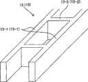
图1(a)是表示形成有本发明的实施例1之半导体器件1的晶片100的一部分的俯视图。在晶片100上格子状地设置有成为划片时的切割区的划片线200,通过沿着划片线200进行划片,而将半导体器件1切割为单片化的芯片。半导体器件1在以包围其周围的方式形成的划线200的附近形成有密封环10。即,密封环10形成在被切割成芯片的半导体器件1的端面附近,并且以包围形成有电路部分的有源区域20的 方式,形成为筒形形状。由此,密封环10在进行划片等时,可以防止在芯片端面附近产生的局部应力向有源区域20传播。 FIG. 1(a) is a plan view showing part of a
图1(b)是图1(a)中以实线包围的区域A的放大图,图2是沿图1(b)中的2-2线的剖视图。如图2所示,半导体器件1由下述部分构成:半导体层21,其形成有晶体管等电路元件;布线层,其在半导体层21的上部,在多个层立体地形成布线。在布线层中,例如层叠有由6个层构成的层间绝缘膜22~27,在该层间绝缘膜22~27内形成有构成多层布线的接触插塞31、通孔插塞33和35、第1~第3布线32、34、36,此外,在芯片端面的附近,以贯通层间绝缘膜22~27的方式形成有密封环10。 Fig. 1(b) is an enlarged view of the area A surrounded by a solid line in Fig. 1(a), and Fig. 2 is a cross-sectional view along line 2-2 in Fig. 1(b). As shown in FIG. 2 , the
第1层间绝缘膜22,是在半导体层21上形成的、形成金属布线前的平坦化膜,其消除在基板工序中所形成的所有台阶。作为第1层间绝缘膜22的材料,例如使用BPSG等。在第1层间绝缘膜22内,形成有和半导体层21上形成的电路元件进行电连接的接触插塞31、以及在密封环10的下方形成的插塞11。接触插塞31和插塞11,例如利用钨等形成。 The first
第2、第4和第6层间绝缘膜23、25、27分别具有依次层叠了防止扩散膜23a、25a、27a、low-k膜23b、25b、27b、帽(cap)膜23c、25c、27c的层叠构造。另一方面,第3和第5层间绝缘膜24、26分别具有依次层叠了防止扩散膜24a、26a、low-k膜24b、26b的层叠构造。防止扩散膜23a~27a例如由SiN或SiC等构成,作为用于防止布线和密封环的构成材料Cu的扩散的屏障层发挥作用。帽膜23c、25c、27c例如由SiO2、SiC、SiOC、SiCN、SiN、SiON等构成,发挥作为low-k膜23b~27b的表面保护膜的功能。low-k膜23b~27b为了抑制RC延迟,由介电常数比较低的例如甲基倍半硅氧烷(MSQ:methylsilsesquioxane)、氢倍半硅氧烷(HSQ:hydrogensilsesquioxane)、CDO膜(Carbon-Doped Oxide)、高分子膜(聚酰亚胺(polyimide)类、聚对二甲苯(parylene)类、特富龙(注册商标)类、其它聚合类)、非结晶碳膜等形成。并且,作为low-k膜所使用的材料的相对介电常数最好在3.0以下。 The second, fourth, and sixth
第1布线32形成在第2层间绝缘膜23内,第2布线34形成在第4 层间绝缘膜25内,第3布线36形成在第6层间绝缘膜27内。第1布线32通过接触插塞31而和形成于半导体层21的电路元件进行电连接。通孔插塞33形成在第3层间绝缘膜24内,使第1布线32和第2布线34进行电连接。通孔插塞35形成在第5层间绝缘膜26内,使第2布线34和第3布线36进行电连接。这些布线和通孔插塞为了抑制RC延迟,而使用电阻比较低的Cu。Cu因为扩散系数大,容易在硅和层间绝缘膜内扩散,所以为了防止Cu的扩散,这些布线和通孔插塞的表面,例如,形成了由Ta、TaN、W、WN、WSi、Ti、TiN、TiSiN等构成的屏障金属层32a~36a。 The
密封环10是对各层间绝缘膜22~27内形成的各构成部分进行结合而构成的。即,密封环10由下述部分构成:第1密封布线12,其形成在第2层间绝缘膜23内,并和插塞11连接;第2密封布线14,其形成在第4层间绝缘膜25内;第3密封布线16,其形成在第6层间绝缘膜27内;密封插塞13,其在第3层间绝缘膜24内,与第2密封布线14一体形成,并也和第1密封布线12连接;密封插塞15,其在第5层间绝缘膜26内,与第3密封布线16一体形成,并也和第2密封布线14连接。即,密封环10,通过交替地层叠密封布线和密封插塞,而以贯通层间绝缘膜23~27的方式形成。这些密封布线和密封插塞,和在有源区域20上形成的多层布线一样,都由铜形成。因此,为了防止Cu向层间绝缘膜内扩散,在密封布线和密封插塞的表面也形成了由Ta、TaN、W、WN、WSi、Ti、TiN、TiSiN等构成的屏障金属层12a~16a。 The
在这里,图1(b)是包括密封环10的半导体器件1的俯视图,在形成有密封10的部分,为了能够理解内部的密封插塞13、15的构造而利用虚线表示了形成密封插塞的部分。图3是仅抽出了密封插塞13、15的立体图。如图1~图3所示,密封插塞13、15由下述部分构成:2个筒状插塞13-1、15-1,其沿着密封10的延伸方向相互分离、并且呈平行设置的筒状;壁部13-2、15-2,其在上述二重构造的筒状插塞之间,以大致和上述插塞垂直相交的方式等间隔地配置,并且和筒状插塞13-1、15-1连接。即,如图1和图3所示,密封插塞13、15由二重构造的筒状插塞13-1、15-1,和与之以正交方式连接的壁部13-2、15-2构成梯形构造体。密封插塞13、15通过采用上述构造,可以提高密封环的机械强度。即,通过密封插塞13、15构成沿密封环10的2个平行的 筒状插塞13-1、15-1,密封环10部分变为2重构造,所以和以单一构造构成筒状插塞的情况相比,机械强度提高了。并且,因为在由2个平行的构造体构成的筒状插塞13-1、15-1之间,等间隔地形成与之大致垂直相交的壁部13-2、15-2,所以加强了整个密封环的强度,密封环10的机械强度进一步提高。由此,即使在由于使用脆弱的low-k膜而导致加到密封环10上的应力相对增加的情况下,也能够避免密封环自身发生破坏这一不良现象。 Here, FIG. 1( b ) is a plan view of a
图4是和以往的密封环进行比较的、表示本实施例的密封环构造的效果的图。划片等时在芯片端面附近所产生的应力,被施加到密封环10上,如图4所示,在以单一构造形成的以往的密封环构造的情况下,对从外部施加的应力的抗力小,因而所施加的应力的大部分加到密封环10上。与此相对,在本实施例的密封环的情况下,因为在二重构造的筒状插塞13-1、15-1之间以与之大致垂直相交的方式形成有壁部13-2、15-2,所以,对所施加的应力的抗力发挥作用,施加到构成密封环10的其它部分、即密封布线和筒状插塞上的应力就大幅度减小,从而可以提高整个密封环的应力耐性。更详细而言,因为应力的作用方向和壁部13-2、15-2的长度方向基本一致,所以能确保壁部13-2、15-2自身的应力耐性。因为壁部13-2、15-2受到来自外部的应力而产生作为其反作用力的抗力,所以,将大幅度地减小加到密封环的构成部分中壁部以外的其它构成部分上的应力,从而整个密封环的应力耐性提高。 FIG. 4 is a diagram showing the effect of the seal ring structure of this embodiment in comparison with a conventional seal ring. The stress generated near the end face of the chip during dicing is applied to the
接下来,参照图5所示的制造工序图,对具有上述构造的半导体器件1的制造方法进行说明。首先,经过公知的电路元件形成工序,在半导体层21(晶片)的有源区域20内形成晶体管等电路元件。然后,在形成了电路元件的晶片上淀积例如PBSG膜,之后,在大约850℃的N2 气氛中实施回流平坦化处理,形成第1层间绝缘膜22。之后,在平坦化之后的BPSG膜上形成用于形成接触插塞31和插塞11的开口。然后,利用使用WF6和H2作为反应气体的CVD法,以嵌入上述开口内部的方式淀积钨,形成接触插塞31和插塞11。之后,利用CMP法等除去淀积在第1层间绝缘膜22上的多余的钨,并且使第1层间绝缘膜22平坦化(图5(a))。 Next, a method of manufacturing the
然后,在第1层间绝缘膜22上形成第2层间绝缘膜23。首先,利用等离子体CVD法在第1层间绝缘膜22上淀积5~200nm左右的SiN 膜,形成防止扩散膜23a。通过形成该防止扩散膜23a来防止构成布线和密封环的Cu向第1层间绝缘膜22内扩散。然后,在防止扩散膜23a上形成厚度100~5000nm左右的low-k膜23b。作为low-k膜的材料,例如可以使用甲基倍半硅氧烷(MSQ),作为其形成方法可以使用SOD(Spin on dielectrics)法,即、在旋涂(spin coating)溶液之后,实施热处理,而形成薄膜。另外,作为low-k膜的形成方法,不限于涂敷法,也可以使用CVD法来形成。此外,也可以在形成low-k膜23b之后,向low-k膜23b的表面照射氦等离子体来进行表面改质处理。由此,来改善和low-k膜23b上所形成的帽膜23c的接合性,从而很难发生界面剥离。然后,利用使用SiH4和O2作为反应气体的CVD法在low-k膜23b上淀积5~200nm左右的SiO2膜,形成帽膜23c。该帽膜23c除了发挥作为low-k膜23b的表面保护膜的功能之外,还发挥作为对low-k膜实施后述的蚀刻处理时的硬掩模的功能。由以上的防止扩散膜23a、low-k膜23b、帽膜23c形成第2层间绝缘膜23。然后,在帽膜23c上形成在要形成第1布线32和第1密封布线12的部位具有开口的光掩模,利用各向异性干式蚀刻处理,对帽膜23c、low-w膜23b以及防止扩散膜23a进行蚀刻,形成布线槽40a和40b(图5(b)),布线槽40a和40b用于利用镶嵌法形成第1布线32和第1密封布线12。 Then, the second
然后,利用溅射法在之前的工序中所形成的布线槽40a和40b的底面和侧面上淀积2~50nm的TiN膜,形成屏障金属层12a和32a。通过形成屏障金属层,来防止作为布线32和第1密封布线12的材料的Cu的扩散。此外,作为屏障金属层的形成方法,也可以采用使用TiCl4和NH3作为反应气体的CVD法。然后,利用电镀法,以填充布线槽40a和40b的方式淀积Cu膜,形成第1布线32并形成第1密封布线12。另外,也可以在实施Cu镀层之前,利用CVD法在形成了屏障金属层的布线槽40a和40b内淀积Cu,生成电镀籽层。然后,例如在250℃的N2气氛中进行退火处理。之后,利用CMP法除去淀积在帽层23c上的Cu,并且进行表面的平坦化处理。在该Cu除去工序中,作为能确保高研磨率且晶片面内的研磨率的均匀性的研磨条件,例如最好设定为研磨压力为2.5~4.5psi、研磨垫(pad)和晶片间的相对速度为60~80m/min。由此,在布线槽40a和40b内利用镶嵌法形成第1布线32和第1密封布线12(图5(c))。 Then, a TiN film of 2 to 50 nm is deposited on the bottom and side surfaces of the
然后,在形成了第1布线32和第1密封布线12的晶片上依次形成第3层间绝缘膜24和第4层间绝缘膜25。第3层间绝缘膜由防止扩散膜24a和low-k膜24b构成,第4层间绝缘膜25由防止扩散膜25a和low-k膜25b以及帽层25c构成。这些构成第3和第4层间绝缘膜的防止扩散膜、low-k膜和帽膜,利用和上述第2层间绝缘膜的形成方法相同的方法形成。在形成了第3和第4层间绝缘膜24和25之后,在帽膜25c上形成在要形成通孔插塞33和密封插塞13的部位上具有开口的光掩模,利用各向异性干式蚀刻对第3和第4层间绝缘膜24和25进行蚀刻,形成用于形成通孔插塞33和密封插塞13的布线槽41a和41b(图5(d))。并且,最好以相同规格来形成布线槽41a和41b的宽度尺寸。 Then, the third
然后,在帽膜25c上形成在要形成第2布线34和第2密封布线14的部位具有开口的光掩模,利用各向异性干式蚀刻处理对第4层间绝缘膜25进行蚀刻,形成用于形成第2布线34和第2密封布线14的布线槽42a和42b(图5(e))。 Then, on the
接下来,利用溅射法,在上述工序中在第3和第4层间绝缘膜内形成的布线槽41a、41b、42a、42b的底面和侧面上淀积TiN膜,形成屏障金属层13a、14a、33a、34a。然后利用电镀法,以填充布线槽41a、41b、42a、42b的方式淀积Cu膜,形成通孔插塞33和第2布线34,并且形成密封插塞13和第2密封布线14。即,利用一举形成通孔部和布线部的双镶嵌法形成通孔插塞33和第2布线34、以及密封插塞13和第2密封布线14。在形成了Cu膜后,例如,在250℃的N2气氛中进行退火处理。之后,利用CMP法除去淀积在帽层25c上的Cu,并进行表面的平坦化处理(图5(f))。 Next, by sputtering, a TiN film is deposited on the bottom and side surfaces of the
接下来,在经过上述工序后的晶片上依次形成第5层间绝缘膜26和第6层间绝缘膜27。第5层间绝缘膜和第3层间绝缘膜一样,由防止扩散膜26a和low-k膜26b构成,第6层间绝缘膜27和第2及第4层间绝缘膜一样,由防止扩散膜27a、low-k膜27b和帽膜27c构成。这些构成第5和第6层间绝缘膜的防止扩散膜、low-k膜以及帽膜,利用和上述第2层间绝缘膜的形成方法相同的方法形成。接下来,在第5层间绝缘膜26和第6层间绝缘膜27内形成用于形成第3布线36的布线槽44b、用于形成通孔插塞35的布线槽43b、用于形成密封布线16的布线槽44a、以及用于形成密封插塞15的布线槽43a。这些布线槽,利 用和在上述第3及第4层间绝缘膜24及25内形成的布线槽的形成方法相同的方法来形成(图5(g))。 Next, a fifth
接下来,利用溅射法,在上述工序中在第5和第6层间绝缘膜内所形成的布线槽43a、43b、44a、44b的底面和侧面上淀积TiN膜,形成屏障金属层15a、16a、35a、36a。然后,利用电镀法,以填充布线槽43a、43b、44a、44b的方式淀积Cu膜,形成通孔插塞35和第3布线36,并形成密封插塞15和密封布线16。即,利用一举形成通孔部和布线部的双镶嵌法来形成通孔插塞35和第3布线36、以及密封插塞15和密封布线16。在形成了Cu膜之后,例如,在250℃的N2气氛中进行退火处理。之后,利用CMP法除去淀积在帽层25c上的Cu,并进行表面的平坦化处理(图5(h))。经过以上工序就完成了本发明的半导体器件1。 Next, by sputtering, a TiN film is deposited on the bottom and side surfaces of the
另外,在本实施例中,使用双镶嵌法来同时形成密封环和多层布线,即同时形成密封插塞、密封布线和通孔插塞、电路布线,但是也可以使用单镶嵌法。即,在这种情况下,在层间绝缘膜内形成密封插塞和通孔插塞后,形成上层的层间绝缘膜,利用镶嵌法仅形成密封布线和电路布线部分。 In addition, in this embodiment, the dual damascene method is used to simultaneously form the seal ring and the multilayer wiring, that is, the seal plug, the seal wiring and the via plug, and the circuit wiring are simultaneously formed, but a single damascene method may also be used. That is, in this case, after the sealing plug and the via plug are formed in the interlayer insulating film, an upper interlayer insulating film is formed, and only the sealing wiring and the circuit wiring portion are formed by the damascene method. the
(实施例2) (Example 2)
接下来,参照附图对本发明的实施例2的半导体器件2的结构进行说明。实施例2中的半导体器件2,其构成密封环的密封插塞的构造与上述实施例1中的不同。图6是对本实施例中的半导体器件的密封环50进行了放大的俯视图,图7是沿图6的7-7线的剖视图。在图6中,和上述实施例1一样,利用虚线表示形成密封插塞的部分,以便能够理解内部的密封插塞的构造。图8是仅抽出本实施例中的密封插塞的立体图。如图7所示,作为构成本实施例中的密封环50的构成部分的密封插塞53,设置在第3层间绝缘膜24内,并和第1密封布线52以及第2密封布线54连接。此外,密封插塞55设置在第5层间绝缘膜26内,并和第2密封布线54以及第3密封布线56连接。如图6和图8所示,密封插塞53、55由下述部分构成:2个筒状插塞53-1、55-1,其沿着密封环50延伸的方向相互分离、并且呈平行设置的筒形形状;壁部53-2、55-2,其在上述的二重构造的筒状插塞53-1、55-1之间,以在斜向右的方向和斜向左的方向上交替地和筒状插塞53-1、55-1相交的方式均匀配置。 Next, the structure of the semiconductor device 2 according to Embodiment 2 of the present invention will be described with reference to the drawings. The semiconductor device 2 in Embodiment 2 differs from that in
通过使密封插塞53、55采用上述构造,和实施例1一样,可以提高密封环的机械强度。即,筒状插塞构成沿密封环50的2个平行的构造体,由此,密封环50就部分地变为2重构造,因此,和以单一构造构成筒状插塞的情况相比,提高了机械强度。此外,因为在这2个筒状插塞之间,形成有在斜向右的方向和斜向左的方向上交替地和筒状插塞相交的壁部,所以,加强了筒状插塞的强度,进一步提高了密封环50的机械强度。由此,和实施例1一样,即使由于使用脆弱的low-k膜而导致施加到密封环50上的应力和以往相比增加了,也可以避免密封环自身发生破坏这一不良状况。 By making the seal plugs 53, 55 adopt the above-mentioned structure, as in the first embodiment, the mechanical strength of the seal ring can be improved. That is, the cylindrical plug constitutes two parallel structures along the seal ring 50, whereby the seal ring 50 partially becomes a double structure. Therefore, compared with the case of constituting the cylindrical plug with a single structure, Improved mechanical strength. In addition, since the wall portions intersecting the cylindrical plugs alternately in the oblique right direction and oblique left direction are formed between the two cylindrical plugs, the strength of the cylindrical plugs is strengthened. strength, further improving the mechanical strength of the sealing ring 50. Thus, as in Example 1, even if the stress applied to the seal ring 50 is increased compared with conventional ones due to the use of a fragile low-k film, the failure of the seal ring itself to be broken can be avoided. the
本实施例的半导体器件2,可以利用和上述实施例1的半导体器件1相同的制造工艺来制造,可以通过变更实施例1的在形成密封插塞53、55时所使用的光掩模的形状来制作。 The semiconductor device 2 of this embodiment can be manufactured by the same manufacturing process as the
根据以上的说明可知,根据本发明的半导体器件,在交替地层叠密封布线和密封插塞而构成的密封环中,构成密封环的筒状插塞呈二重构造,并以和筒状插塞正交或斜向地相交的方式设置有壁部,所以,和未设置壁部的以往构造的密封环相比,可以提高密封环自身的强度。因此,即使在随着构成布线层的层间绝缘膜的低介电常数化,其机械强度变得更加脆弱,施加应力时加到密封环上的负荷进一步增加的情况下,也能防止密封环本身发生破坏。此外,由于密封环的机械强度增加,密封环自身变得不易被破坏,因此,也可降低所施加的应力向密封环内部的有源区域传播、给电路部分带来不良影响的可能性。 As can be seen from the above description, according to the semiconductor device of the present invention, in the seal ring formed by alternately stacking the seal wiring and the seal plug, the cylindrical plug constituting the seal ring has a double structure, and the cylindrical plug and the cylindrical plug Since the wall portions are provided so as to intersect each other perpendicularly or obliquely, the strength of the seal ring itself can be increased compared to a seal ring of a conventional structure in which no wall portion is provided. Therefore, even if the mechanical strength of the interlayer insulating film constituting the wiring layer becomes weaker as the dielectric constant becomes lower, and the load applied to the seal ring when stress is applied further increases, the seal ring can be prevented from being damaged. damage itself. In addition, since the mechanical strength of the seal ring is increased, the seal ring itself is less likely to be damaged, so the possibility of the applied stress propagating to the active region inside the seal ring and adversely affecting the circuit portion can also be reduced. the
(变形例) (Modification)
图9(a)~(d)是表示密封环的其它构造例子的俯视图。图9(a)和实施例1中的密封环构造相似,在筒状插塞由相互分离并且平行的三个构造体构成这一点上与实施例1不同。图9(b)和实施例2中的密封环构造相似,在平行的两个筒状插塞之间,在斜向右的方向和斜向左的方向与筒状插塞相交的壁部的构成部分,呈现在筒状插塞的大致中间部位相交的状态。即,以X形构成壁部。图9(c)和图9(b)所示的构造相比,筒状插塞由相互分离并且平行的三个构造体构成。图9(d)将壁部设计成所谓的蜂窝(Honeycomb)构造。通过将密封环的构造设置成如上述各变形例的构造,可以进一步提高密封环的机械强度。 9( a ) to ( d ) are plan views showing other structural examples of seal rings. FIG. 9( a ) is similar to the structure of the seal ring in Example 1, but differs from Example 1 in that the cylindrical plug is composed of three structures separated from each other and parallel to each other. Figure 9(b) is similar to the structure of the sealing ring in Example 2, between two parallel cylindrical plugs, the wall portion intersecting the cylindrical plugs in the oblique right direction and oblique left direction The constituent parts intersect at approximately the middle of the cylindrical plug. That is, the wall portion is formed in an X shape. Compared with the structures shown in FIG. 9( c ) and FIG. 9( b ), the cylindrical plug is composed of three structures separated from each other and parallel to each other. FIG. 9( d ) designs the wall into a so-called honeycomb structure. The mechanical strength of the seal ring can be further improved by providing the structure of the seal ring as in the above-mentioned modification examples. the
Claims (8)
Translated fromChineseApplications Claiming Priority (3)
| Application Number | Priority Date | Filing Date | Title |
|---|---|---|---|
| JP2007176204AJP5106933B2 (en) | 2007-07-04 | 2007-07-04 | Semiconductor device |
| JP2007-176204 | 2007-07-04 | ||
| JP2007176204 | 2007-07-04 |
Publications (2)
| Publication Number | Publication Date |
|---|---|
| CN101339924A CN101339924A (en) | 2009-01-07 |
| CN101339924Btrue CN101339924B (en) | 2012-04-04 |
Family
ID=40213949
Family Applications (1)
| Application Number | Title | Priority Date | Filing Date |
|---|---|---|---|
| CN200810097711XAExpired - Fee RelatedCN101339924B (en) | 2007-07-04 | 2008-05-20 | Semiconductor device |
Country Status (4)
| Country | Link |
|---|---|
| US (1) | US20090008750A1 (en) |
| JP (1) | JP5106933B2 (en) |
| KR (1) | KR20090004469A (en) |
| CN (1) | CN101339924B (en) |
Families Citing this family (23)
| Publication number | Priority date | Publication date | Assignee | Title |
|---|---|---|---|---|
| JP5423029B2 (en)* | 2009-02-12 | 2014-02-19 | 富士通セミコンダクター株式会社 | Manufacturing method of semiconductor device |
| US8643149B2 (en)* | 2009-03-03 | 2014-02-04 | Taiwan Semiconductor Manufacturing Company, Ltd. | Stress barrier structures for semiconductor chips |
| KR101581431B1 (en) | 2009-09-04 | 2015-12-30 | 삼성전자주식회사 | Semiconductor chips having guard rings and methods of fabricating the same |
| US8624348B2 (en) | 2011-11-11 | 2014-01-07 | Invensas Corporation | Chips with high fracture toughness through a metal ring |
| US20150111005A1 (en)* | 2012-05-08 | 2015-04-23 | Asahi Kasei E-Materials Corporation | Transfer method and thermal nanoimprinting apparatus |
| JP6093556B2 (en)* | 2012-11-13 | 2017-03-08 | 富士通株式会社 | Semiconductor device, semiconductor integrated circuit device, and electronic device |
| CN104701271A (en) | 2013-12-05 | 2015-06-10 | 中芯国际集成电路制造(上海)有限公司 | Semiconductor structure and forming method thereof |
| CN105990313B (en)* | 2015-02-17 | 2019-01-29 | 中芯国际集成电路制造(上海)有限公司 | A kind of sealing ring of chip |
| JPWO2018020713A1 (en)* | 2016-07-28 | 2019-05-09 | パナソニックIpマネジメント株式会社 | Semiconductor device and method of manufacturing the same |
| JP6419762B2 (en)* | 2016-09-06 | 2018-11-07 | 株式会社Kokusai Electric | Semiconductor device manufacturing method, substrate processing apparatus, and program |
| US9728474B1 (en) | 2016-09-28 | 2017-08-08 | Globalfoundries Singapore Pte. Ltd. | Semiconductor chips with seal rings and electronic test structures, semiconductor wafers including the semiconductor chips, and methods for fabricating the same |
| JP6230676B2 (en)* | 2016-10-11 | 2017-11-15 | ルネサスエレクトロニクス株式会社 | Semiconductor device |
| US10790240B2 (en)* | 2017-03-17 | 2020-09-29 | Taiwan Semiconductor Manufacturing Co., Ltd. | Metal line design for hybrid-bonding application |
| CN107452756B (en) | 2017-07-28 | 2020-05-19 | 京东方科技集团股份有限公司 | Thin film transistor structure, manufacturing method thereof, display panel and display device |
| US10804140B2 (en)* | 2018-03-29 | 2020-10-13 | Taiwan Semiconductor Manufacturing Co., Ltd. | Interconnect formation and structure |
| US10381403B1 (en)* | 2018-06-21 | 2019-08-13 | Globalfoundries Singapore Pte. Ltd. | MRAM device with improved seal ring and method for producing the same |
| CN112292757B (en)* | 2018-08-24 | 2024-03-05 | 铠侠股份有限公司 | Semiconductor device and manufacturing method thereof |
| CN111564411B (en)* | 2020-06-08 | 2022-12-23 | 深圳铨力半导体有限公司 | Semiconductor device and forming method thereof |
| US11373962B2 (en) | 2020-08-14 | 2022-06-28 | Taiwan Semiconductor Manufacturing Co., Ltd. | Advanced seal ring structure and method of making the same |
| CN113053828B (en)* | 2021-03-12 | 2022-05-27 | 长鑫存储技术有限公司 | Sealing ring and forming method thereof |
| US20230029241A1 (en)* | 2021-07-22 | 2023-01-26 | Taiwan Semiconductor Manufacturing Company, Ltd. | Seal ring structures |
| US12300636B2 (en)* | 2021-07-29 | 2025-05-13 | Taiwan Semiconductor Manufacturing Company, Ltd | Seal ring structure and method of fabricating the same |
| US12342695B2 (en)* | 2021-09-30 | 2025-06-24 | Yunnan Invensight Optoelectronics Technology Co., Ltd. | Display substrate, display motherboard and display panel related thereto |
Citations (1)
| Publication number | Priority date | Publication date | Assignee | Title |
|---|---|---|---|---|
| CN1519924A (en)* | 2003-02-03 | 2004-08-11 | �����ɷ� | Semiconductor device and manufacturing method thereof |
Family Cites Families (9)
| Publication number | Priority date | Publication date | Assignee | Title |
|---|---|---|---|---|
| JP3813562B2 (en)* | 2002-03-15 | 2006-08-23 | 富士通株式会社 | Semiconductor device and manufacturing method thereof |
| JP4519411B2 (en)* | 2003-04-01 | 2010-08-04 | ルネサスエレクトロニクス株式会社 | Semiconductor device |
| US20050035455A1 (en)* | 2003-08-14 | 2005-02-17 | Chenming Hu | Device with low-k dielectric in close proximity thereto and its method of fabrication |
| JP2005129717A (en)* | 2003-10-23 | 2005-05-19 | Renesas Technology Corp | Semiconductor device |
| JP4280204B2 (en)* | 2004-06-15 | 2009-06-17 | Okiセミコンダクタ株式会社 | Semiconductor device |
| JP2006190839A (en)* | 2005-01-06 | 2006-07-20 | Matsushita Electric Ind Co Ltd | Semiconductor device and manufacturing method thereof |
| JP2006351878A (en)* | 2005-06-16 | 2006-12-28 | Matsushita Electric Ind Co Ltd | Semiconductor device |
| US7622364B2 (en)* | 2006-08-18 | 2009-11-24 | International Business Machines Corporation | Bond pad for wafer and package for CMOS imager |
| US8643147B2 (en)* | 2007-11-01 | 2014-02-04 | Taiwan Semiconductor Manufacturing Company, Ltd. | Seal ring structure with improved cracking protection and reduced problems |
- 2007
- 2007-07-04JPJP2007176204Apatent/JP5106933B2/ennot_activeExpired - Fee Related
- 2008
- 2008-05-20CNCN200810097711XApatent/CN101339924B/ennot_activeExpired - Fee Related
- 2008-05-20KRKR1020080046625Apatent/KR20090004469A/ennot_activeCeased
- 2008-06-20USUS12/142,875patent/US20090008750A1/ennot_activeAbandoned
Patent Citations (1)
| Publication number | Priority date | Publication date | Assignee | Title |
|---|---|---|---|---|
| CN1519924A (en)* | 2003-02-03 | 2004-08-11 | �����ɷ� | Semiconductor device and manufacturing method thereof |
Also Published As
| Publication number | Publication date |
|---|---|
| CN101339924A (en) | 2009-01-07 |
| JP5106933B2 (en) | 2012-12-26 |
| JP2009016542A (en) | 2009-01-22 |
| US20090008750A1 (en) | 2009-01-08 |
| KR20090004469A (en) | 2009-01-12 |
Similar Documents
| Publication | Publication Date | Title |
|---|---|---|
| CN101339924B (en) | Semiconductor device | |
| US11056450B2 (en) | Semiconductor device | |
| JP5324822B2 (en) | Semiconductor device | |
| US7687915B2 (en) | Semiconductor device having crack stop structure | |
| JP4360881B2 (en) | Semiconductor device including multilayer wiring and manufacturing method thereof | |
| TW202006796A (en) | Method for integrated circuit fabrication | |
| KR20180110011A (en) | Semiconductor device and manufacturing method thereof | |
| US20070290361A1 (en) | Via layout with via groups placed in interlocked arrangement | |
| US20060145347A1 (en) | Semiconductor device and method for fabricating the same | |
| US20140273453A1 (en) | Semiconductor device and method for manufacturing semiconductor device | |
| KR101674057B1 (en) | Semiconductor chip structure having a complex reinforced insulator and method of fabricating the same | |
| JP4280204B2 (en) | Semiconductor device | |
| JP2005142351A (en) | Semiconductor device and its manufacturing method | |
| KR100818108B1 (en) | Multi-layer metallization method of semiconductor device using damascene process | |
| KR100871551B1 (en) | Semiconductor device and manufacturing method | |
| JP5932079B2 (en) | Semiconductor device | |
| JP2008041804A (en) | Semiconductor device and manufacturing method thereof | |
| KR101051808B1 (en) | Method of manufacturing semiconductor device using local connection wiring | |
| US20240136291A1 (en) | Low-stress passivation layer | |
| JP5801329B2 (en) | Semiconductor device | |
| JP5214571B2 (en) | Semiconductor device | |
| KR20060011384A (en) | Method of manufacturing semiconductor device using dual damascene process | |
| JP2009105148A (en) | Semiconductor device |
Legal Events
| Date | Code | Title | Description |
|---|---|---|---|
| C06 | Publication | ||
| PB01 | Publication | ||
| C10 | Entry into substantive examination | ||
| SE01 | Entry into force of request for substantive examination | ||
| C14 | Grant of patent or utility model | ||
| GR01 | Patent grant | ||
| ASS | Succession or assignment of patent right | Owner name:OKI SEMICONDUCTOR CO., LTD. Free format text:FORMER OWNER: OKI ELECTRIC INDUSTRY CO., LTD. Effective date:20131108 | |
| C41 | Transfer of patent application or patent right or utility model | ||
| C56 | Change in the name or address of the patentee | ||
| CP01 | Change in the name or title of a patent holder | Address after:Kanagawa Patentee after:LAPIS SEMICONDUCTOR Co.,Ltd. Address before:Kanagawa Patentee before:Oki Semiconductor Co.,Ltd. | |
| TR01 | Transfer of patent right | Effective date of registration:20131108 Address after:Kanagawa Patentee after:Oki Semiconductor Co.,Ltd. Address before:Tokyo, Japan Patentee before:Oki Electric Industry Co.,Ltd. | |
| CF01 | Termination of patent right due to non-payment of annual fee | Granted publication date:20120404 Termination date:20160520 | |
| CF01 | Termination of patent right due to non-payment of annual fee |