CN101335483A - power conversion device - Google Patents
power conversion deviceDownload PDFInfo
- Publication number
- CN101335483A CN101335483ACNA2008101288631ACN200810128863ACN101335483ACN 101335483 ACN101335483 ACN 101335483ACN A2008101288631 ACNA2008101288631 ACN A2008101288631ACN 200810128863 ACN200810128863 ACN 200810128863ACN 101335483 ACN101335483 ACN 101335483A
- Authority
- CN
- China
- Prior art keywords
- electrode
- conduction
- switching element
- voltage
- switching circuit
- Prior art date
- Legal status (The legal status is an assumption and is not a legal conclusion. Google has not performed a legal analysis and makes no representation as to the accuracy of the status listed.)
- Pending
Links
Images


Classifications
- H—ELECTRICITY
- H02—GENERATION; CONVERSION OR DISTRIBUTION OF ELECTRIC POWER
- H02M—APPARATUS FOR CONVERSION BETWEEN AC AND AC, BETWEEN AC AND DC, OR BETWEEN DC AND DC, AND FOR USE WITH MAINS OR SIMILAR POWER SUPPLY SYSTEMS; CONVERSION OF DC OR AC INPUT POWER INTO SURGE OUTPUT POWER; CONTROL OR REGULATION THEREOF
- H02M7/00—Conversion of AC power input into DC power output; Conversion of DC power input into AC power output
- H02M7/42—Conversion of DC power input into AC power output without possibility of reversal
- H02M7/44—Conversion of DC power input into AC power output without possibility of reversal by static converters
- H02M7/48—Conversion of DC power input into AC power output without possibility of reversal by static converters using discharge tubes with control electrode or semiconductor devices with control electrode
- H02M7/53—Conversion of DC power input into AC power output without possibility of reversal by static converters using discharge tubes with control electrode or semiconductor devices with control electrode using devices of a triode or transistor type requiring continuous application of a control signal
- H02M7/537—Conversion of DC power input into AC power output without possibility of reversal by static converters using discharge tubes with control electrode or semiconductor devices with control electrode using devices of a triode or transistor type requiring continuous application of a control signal using semiconductor devices only, e.g. single switched pulse inverters
- H02M7/5387—Conversion of DC power input into AC power output without possibility of reversal by static converters using discharge tubes with control electrode or semiconductor devices with control electrode using devices of a triode or transistor type requiring continuous application of a control signal using semiconductor devices only, e.g. single switched pulse inverters in a bridge configuration
- H—ELECTRICITY
- H02—GENERATION; CONVERSION OR DISTRIBUTION OF ELECTRIC POWER
- H02M—APPARATUS FOR CONVERSION BETWEEN AC AND AC, BETWEEN AC AND DC, OR BETWEEN DC AND DC, AND FOR USE WITH MAINS OR SIMILAR POWER SUPPLY SYSTEMS; CONVERSION OF DC OR AC INPUT POWER INTO SURGE OUTPUT POWER; CONTROL OR REGULATION THEREOF
- H02M1/00—Details of apparatus for conversion
- H02M1/08—Circuits specially adapted for the generation of control voltages for semiconductor devices incorporated in static converters
- H—ELECTRICITY
- H02—GENERATION; CONVERSION OR DISTRIBUTION OF ELECTRIC POWER
- H02M—APPARATUS FOR CONVERSION BETWEEN AC AND AC, BETWEEN AC AND DC, OR BETWEEN DC AND DC, AND FOR USE WITH MAINS OR SIMILAR POWER SUPPLY SYSTEMS; CONVERSION OF DC OR AC INPUT POWER INTO SURGE OUTPUT POWER; CONTROL OR REGULATION THEREOF
- H02M3/00—Conversion of DC power input into DC power output
- H02M3/02—Conversion of DC power input into DC power output without intermediate conversion into AC
- H02M3/04—Conversion of DC power input into DC power output without intermediate conversion into AC by static converters
- H02M3/10—Conversion of DC power input into DC power output without intermediate conversion into AC by static converters using discharge tubes with control electrode or semiconductor devices with control electrode
- H02M3/145—Conversion of DC power input into DC power output without intermediate conversion into AC by static converters using discharge tubes with control electrode or semiconductor devices with control electrode using devices of a triode or transistor type requiring continuous application of a control signal
- H02M3/155—Conversion of DC power input into DC power output without intermediate conversion into AC by static converters using discharge tubes with control electrode or semiconductor devices with control electrode using devices of a triode or transistor type requiring continuous application of a control signal using semiconductor devices only
- H02M3/156—Conversion of DC power input into DC power output without intermediate conversion into AC by static converters using discharge tubes with control electrode or semiconductor devices with control electrode using devices of a triode or transistor type requiring continuous application of a control signal using semiconductor devices only with automatic control of output voltage or current, e.g. switching regulators
- H02M3/158—Conversion of DC power input into DC power output without intermediate conversion into AC by static converters using discharge tubes with control electrode or semiconductor devices with control electrode using devices of a triode or transistor type requiring continuous application of a control signal using semiconductor devices only with automatic control of output voltage or current, e.g. switching regulators including plural semiconductor devices as final control devices for a single load
- H02M3/1588—Conversion of DC power input into DC power output without intermediate conversion into AC by static converters using discharge tubes with control electrode or semiconductor devices with control electrode using devices of a triode or transistor type requiring continuous application of a control signal using semiconductor devices only with automatic control of output voltage or current, e.g. switching regulators including plural semiconductor devices as final control devices for a single load comprising at least one synchronous rectifier element
- Y—GENERAL TAGGING OF NEW TECHNOLOGICAL DEVELOPMENTS; GENERAL TAGGING OF CROSS-SECTIONAL TECHNOLOGIES SPANNING OVER SEVERAL SECTIONS OF THE IPC; TECHNICAL SUBJECTS COVERED BY FORMER USPC CROSS-REFERENCE ART COLLECTIONS [XRACs] AND DIGESTS
- Y02—TECHNOLOGIES OR APPLICATIONS FOR MITIGATION OR ADAPTATION AGAINST CLIMATE CHANGE
- Y02B—CLIMATE CHANGE MITIGATION TECHNOLOGIES RELATED TO BUILDINGS, e.g. HOUSING, HOUSE APPLIANCES OR RELATED END-USER APPLICATIONS
- Y02B70/00—Technologies for an efficient end-user side electric power management and consumption
- Y02B70/10—Technologies improving the efficiency by using switched-mode power supplies [SMPS], i.e. efficient power electronics conversion e.g. power factor correction or reduction of losses in power supplies or efficient standby modes
Landscapes
- Engineering & Computer Science (AREA)
- Power Engineering (AREA)
- Power Conversion In General (AREA)
- Inverter Devices (AREA)
Abstract
Translated fromChinese
Description
Translated fromChinese技术领域technical field
本发明涉及一种用于驱动电压驱动型晶体管的栅极驱动电路(gatedrive circuit),特别是涉及一种在由电压驱动型晶体管对大电流进行开关控制的电力变换装置或对电感负载的施加电压或电流进行控制的电力变换装置上使用的栅极驱动电路。The present invention relates to a gate drive circuit (gate drive circuit) for driving a voltage-driven transistor, in particular to a power conversion device in which a large current is switched by a voltage-driven transistor or an applied voltage to an inductive load. Or a gate drive circuit used in a power conversion device that controls current.
背景技术Background technique
在用于产业用机器或混合动力汽车的电力变换装置中,作为高效率地开关控制大电流的元件,使用MOSFET(Metal-Oxide-Semiconductor FieldEffect Transistor)或IGBT(Insulated Gate bipolar Transistor)等的电压驱动型晶体管。在开关控制大电流时,为了保护元件不受浪涌电压的影响,需要增大栅极(gate)电阻并缓慢进行开关。In power conversion devices used in industrial equipment and hybrid vehicles, voltage drives such as MOSFETs (Metal-Oxide-Semiconductor Field Effect Transistor) and IGBTs (Insulated Gate Bipolar Transistor) are used as elements that efficiently switch and control large currents type transistor. When switching and controlling a large current, in order to protect the device from surge voltage, it is necessary to increase the gate resistance and switch slowly.
但是,缓慢进行开关会使开关时间和开关损失增加,造成系统的电压的利用率或效率降低的不良影响。为了高度地兼顾存在于浪涌电压、和开关时间及开关损失之间的平衡,设法在栅极驱动电路设置有源钳位电路或可变栅极电阻电路等。However, slow switching increases the switching time and switching loss, which adversely affects the utilization rate or efficiency of the voltage of the system. In order to achieve a high balance between surge voltage, switching time, and switching loss, an active clamp circuit or a variable gate resistance circuit is provided in the gate drive circuit.
利用图2,对技术问题进行说明。MOSFET 1具有源电极11、漏电极12和栅电极13。通过控制源电极11和漏电极13之间的电位差,来控制源电极11和漏电极12之间的导通/非导通。为了控制MOSFET 1的导通/非导通,将栅极驱动指令3输入电压切换电路4来切换栅极电压。Using Fig. 2, the technical problem will be described.
电压切换电路4接受栅极ON指令31后,栅极ON用开关41闭合,从栅极驱动用电源2通过ON用栅极电阻51向寄生于栅电极13上的栅极输入电容供给电荷。其结果,MOSFET成为ON,源电极11和漏电极12之间导通。When the
另外,接受栅极OFF指令32后,栅极OFF用开关42闭合,通过OFF用栅极电阻52短接栅电极13和源电极11之间,栅极输入电容的电荷放电。其结果,MOSFET1 OFF,源电极11和漏电极12之间成为非导通。In addition, when the
这里,确定将MOSFET 1 OFF的速度的是OFF用栅极电阻52。若OFF用栅极电阻52增大,由于电荷放电缓慢,开关时间变长,造成由电压利用率的降低或开关损失的增加而引起的元件温度上升的不良影响。另一方面,可以通过切断的电流路径的电感成分来抑制源电极11和漏电极12之间重叠的浪涌电压的峰值。Here, it is the
相反地,若OFF用栅极电阻52减小,由于电荷放电快速,可以使开关时间缩短,具有提高电压利用率和降低开关损失的效果,但是,浪涌电压的峰值会变大,需要考虑和MOSFET 1的耐压破坏和EMC噪声增加等的影响的平衡。Conversely, if the
在图3表示在MOSFET 1截止时的栅极-源极间电压和漏极-源极间电压的波形。Figure 3 shows the waveforms of the gate-source voltage and the drain-source voltage when
在区间t1中,在栅极切断的阈值附近,ON时的栅极电压放电。区间t1的长度由OFF用栅极电阻52和MOSFET 1的栅极输入电容的积决定。在t2区间,漏极-源极间电压上升,并且,在OFF用栅极电阻52吸引由MOSFET 1的米勒电容流入的电荷。由于通过吸引由米勒电容流入的电荷的程度来决定漏极-源极间的电压变化率,所以在这个区间的栅极电阻的值决定浪涌电压。In the interval t1, the gate voltage at the ON time is discharged near the gate cut-off threshold. The length of the interval t1 is determined by the product of the
若为了缩短开关时间而使OFF用栅极电阻52减小,则如图4所示,可以缩短区间t1的长度以及区间t2的长度。但是,有浪涌电压变大的弊病。为了抑制浪涌电压并同时缩短开关时间,需要尽可能减小对浪涌电压未影响的区间t1,还要将决定浪涌电压的区间t2调整为适当的时间。If the
另外,在短路和过电流的切断中,虽然需要尽可能设法增大栅极电阻来抑制浪涌电压,但栅极电阻增大时,由于区间t1增加,所以会成为电流切断迟缓的原因,有在迟缓的部分电流会增加的弊病。In addition, in the interruption of short circuit and overcurrent, although it is necessary to increase the gate resistance as much as possible to suppress the surge voltage, when the gate resistance increases, the interval t1 increases, so it will cause the current interruption to be delayed. The disadvantage that the current will increase in the sluggish part.
这里,在特开2000-77537号公报(专利文献1)中,使用了栅极驱动电路,该栅极驱动电路利用在栅极-漏极间由齐纳二极管构成的有源钳位电路。有源钳位电路在栅极-漏极之间由用于将在漏电极产生的浪涌电压反馈给栅极的齐纳二极管、和防止在栅极ON时从栅极到漏极的电荷的流出的逆接防止二极管构成。Here, in Japanese Unexamined Patent Publication No. 2000-77537 (Patent Document 1), a gate drive circuit using an active clamp circuit composed of a Zener diode between the gate and the drain is used. The active clamp circuit consists of a Zener diode between the gate and the drain to feed back the surge voltage generated at the drain electrode to the gate, and a device that prevents charge from the gate to the drain when the gate is ON. Outflow reverse connection prevents diode formation.
漏极-源极间的浪涌电压若超过齐纳二极管的齐纳电压,则漏极-栅极间导通,抬高栅极电压。因此,可以将漏极-源极间电压钳位在齐纳电压加上栅极阈电压的电压值附近。由于浪涌电压可以通过齐纳电压加上栅极阈电压的电压值限制,所以可以使OFF用栅极电阻相对较小。其结果,可以缩短区间和t1,高度地兼顾浪涌电压和开关时间的平衡。When the surge voltage between the drain and the source exceeds the Zener voltage of the Zener diode, the drain and the gate are turned on and the gate voltage is raised. Therefore, the voltage between the drain and the source can be clamped to a voltage value near the Zener voltage plus the gate threshold voltage. Since the surge voltage can be limited by the voltage value of the Zener voltage plus the gate threshold voltage, the gate resistance for OFF can be relatively small. As a result, the interval and t1 can be shortened, and the balance between the surge voltage and the switching time can be achieved at a high level.
但是,由齐纳二极管流入的电荷被OFF用栅极电阻消耗,若过分减小电阻值则电阻的消耗功率就会增大。因此,OFF用栅极电阻需要使用额定功率较大的电阻。为了抑制消耗功率,作为栅极电阻要求的要素,希望在区间t1中减小电阻值,在齐纳二极管导通的区间t2中电阻值较大。该技术问题,在图2所示的只使用固定电阻的栅极驱动电路和以前相比没有变化。However, the charge flowing through the Zener diode is consumed by the OFF gate resistor, and if the resistance value is reduced too much, the power consumption of the resistor will increase. Therefore, it is necessary to use a resistor with a large power rating for the gate resistor for OFF. In order to suppress power consumption, it is desirable to reduce the resistance value in the interval t1 as an element required for the gate resistance, and to increase the resistance value in the interval t2 in which the Zener diode conducts. This technical problem has not changed in the gate drive circuit shown in Figure 2 using only fixed resistors compared to the previous ones.
另外,在特开2002-369495号公报(专利文献2)中,为了解决上述技术问题,使用了根据区间切换OFF用栅极电阻的电阻值的栅极驱动电路。In addition, in JP-A-2002-369495 (Patent Document 2), in order to solve the above-mentioned technical problems, a gate drive circuit that switches the resistance value of the gate resistor for OFF according to the section is used.
在本文献的图1中,具有第一OFF用栅极电阻R1和第二OFF用栅极电阻R2,通过各个第一栅极OFF用开关Q2和第二栅极OFF用开关Q3切换和源极电位的导通。另外,截止初期使Q2和Q3两方ON,通过R1和R2的并联电阻快速吸引栅极电荷,漏极电压或栅极电压成为规定的电压后Q2闭合,只用R2使MOSFET 1截止,实现希望的栅极特性。但是,用于对漏极电压或栅极电压进行监视的电路或切换电阻值的电路等,由于电路复杂化,有电路的大规模化、高成本化等的弊病。In FIG. 1 of this document, there is a first OFF gate resistor R1 and a second OFF gate resistor R2, and the source and source are switched by each of the first gate OFF switch Q2 and the second gate OFF switch Q3. Potential conduction. In addition, both Q2 and Q3 are turned ON at the beginning of the cut-off, and the gate charge is quickly attracted by the parallel resistance of R1 and R2. After the drain voltage or gate voltage reaches the specified voltage, Q2 is closed, and only R2 is used to turn off
专利文献1:日本特开2000-77537号公报Patent Document 1: Japanese Patent Laid-Open No. 2000-77537
专利文献2:特开2002-369495号公报Patent Document 2: JP-A-2002-369495
发明内容Contents of the invention
本发明为了解决所述现有技术的问题,目的在于提供一种电力变换装置,高度地兼顾存在于浪涌电压和开关时间、开关损失之间的平衡,并且实现其简单、低成本的电路构成。In order to solve the above-mentioned problems of the prior art, the object of the present invention is to provide a power conversion device that takes into account the balance among surge voltage, switching time, and switching loss, and realizes its simple and low-cost circuit configuration. .
本发明的电力变换装置中的有代表性的一个,其具有:开关元件,其根据施加在控制电极的电压,在从第2电极朝向第1电极的方向上流过主电流;电压切换电路,其控制施加在控制电极上的电压;和导通切换电路,其连接在第2电极和控制电极之间。A typical power conversion device of the present invention includes: a switching element for passing a main current in a direction from the second electrode toward the first electrode according to a voltage applied to the control electrode; and a voltage switching circuit for controlling a voltage applied to the control electrode; and conducting a switching circuit connected between the second electrode and the control electrode.
更为优选,在电压切换电路输出使开关元件OFF的信号时,导通切换电路根据第2电极和第1电极间的第1电位差、以及控制电极和第1电极间的第2电位差进行导通控制。More preferably, when the voltage switching circuit outputs a signal for turning off the switching element, the switching circuit is turned on based on a first potential difference between the second electrode and the first electrode, and a second potential difference between the control electrode and the first electrode. conduction control.
另外,更为优选,导通切换电路在第1电位差小于第2电位差时进行导通控制,在第1电位差大于第2电位差时,进行非导通控制。In addition, more preferably, the conduction switching circuit performs conduction control when the first potential difference is smaller than the second potential difference, and performs non-conduction control when the first potential difference is greater than the second potential difference.
对于本发明的其他特征,在后述的实施方式进行说明。Other features of the present invention will be described in the embodiments described later.
根据本发明,可以提供一种抑制浪涌电压的同时缩短开关时间的电力变换装置。According to the present invention, it is possible to provide a power conversion device capable of shortening switching time while suppressing surge voltage.
附图说明Description of drawings
图1是表示本发明的构成的模块图。FIG. 1 is a block diagram showing the configuration of the present invention.
图2是表示现有技术的电路构成图。FIG. 2 is a circuit configuration diagram showing a prior art.
图3是在现有技术中栅极电阻较大的情况下的开关波形图。FIG. 3 is a switching waveform diagram in the case of a large gate resistance in the prior art.
图4是在现有技术中栅极电阻较小的情况下的开关波形图。FIG. 4 is a switching waveform diagram in the case of a relatively small gate resistance in the prior art.
图5是本发明的开关波形图。Fig. 5 is a switching waveform diagram of the present invention.
图6是表示在本发明的实施方式1的电力变换装置的电路图。6 is a circuit diagram showing a power conversion device according to
图7是表示在本发明的实施方式2的电力变换装置的电路图。7 is a circuit diagram showing a power conversion device according to
图8是表示在本发明的实施方式3的电力变换装置的电路图。8 is a circuit diagram showing a power conversion device according to
图9是在实施方式1中使用面安装独立部件时的安装形态。FIG. 9 is a mounting form when surface-mounting individual components are used in
图10是表示本发明的实施方式4的逆变器系统的图。FIG. 10 is a diagram showing an inverter system according to
图11是表示本发明的实施方式5的DCDC变换器的图。FIG. 11 is a diagram showing a DCDC converter according to Embodiment 5 of the present invention.
图12是使用现有技术的情况的波形图。Fig. 12 is a waveform diagram of a case where the prior art is used.
图13是采用本发明的构成的情况的波形图。Fig. 13 is a waveform diagram in the case of adopting the configuration of the present invention.
符号说明Symbol Description
1、111、112、121、122、131、132-MOSFET,2-栅极驱动用电源,3、311、312、321、322、331、332-栅极驱动指令,4、411、412、421、422、431、432-电压切换电路,8、811、812、821、822、831、832-导通切换电路,11-源电极,12-漏电极,13-栅电极,31-栅极ON指令,32-栅极OFF指令,41-栅极ON用开关,42-栅极OFF用开关,51-ON用栅极电阻,52-OFF用栅极电阻,61-主电路寄生电感,62、67-平滑电容器,63、68-蓄电池,64-电动机,65、66-控制器,69-电感器,71-NOT电路,81a-P型MOSFET,81b-N型MOSFET,82-二极管,82a、82b-齐纳二极管,83-旁路用二极管。1, 111, 112, 121, 122, 131, 132-MOSFET, 2-gate drive power supply, 3, 311, 312, 321, 322, 331, 332-gate drive command, 4, 411, 412, 421 , 422, 431, 432-voltage switching circuit, 8, 811, 812, 821, 822, 831, 832-conduction switching circuit, 11-source electrode, 12-drain electrode, 13-gate electrode, 31-gate ON Command, 32-gate OFF command, 41-switch for gate ON, 42-switch for gate OFF, 51-gate resistor for ON, 52-gate resistor for OFF, 61-main circuit parasitic inductance, 62, 67-smoothing capacitor, 63, 68-battery, 64-motor, 65, 66-controller, 69-inductor, 71-NOT circuit, 81a-P type MOSFET, 81b-N type MOSFET, 82-diode, 82a, 82b-zener diode, 83-bypass diode.
具体实施方式Detailed ways
下面,参照附图对本发明的实施方式进行详细说明。Hereinafter, embodiments of the present invention will be described in detail with reference to the drawings.
实施方式1
在图1表示本发明的实施方式1的构成。FIG. 1 shows the configuration of
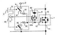
在本实施方式中,说明了使用MOSFET 1作为电压驱动型晶体管(开关元件)的情况。本实施方式的电力变换装置在MOSFET 1的栅电极13(控制电极)和漏电极12之间,具有将二极管82和P型MOSFET 81a串联地连接的导通切换电路8。In this embodiment, a case where the
P型MOSFET 81a的源电极连接于MOSFET 1的栅电极13。P型MOSFET 81a的漏电极连接于二极管82的阳极,二极管82的阴极连接于MOSFET 1的漏电极12。另外,P型MOSFET 81a的栅电极连接于电压切换电路4的栅极OFF用开关42和OFF用栅极电阻52之间。The source electrode of the P-
MOSFET 1在ON稳定的情况下,P型MOSFET 81a的栅极电压通过OFF用栅极电阻52放电。即P型MOSFET 81a处于OFF状态。栅极OFF用开关42闭合,MOSFET 1的截止动作开始后,P型MOSFET 81a导通,MOSFET 1的栅极电荷通过P型MOSFET 81a和二极管82,向MOSFET 1的漏电极放电。通过在该通路上吸引MOSFET 1的栅极电荷,可以缩短表示在图5的区间t1的长度。When the
另外,在该通路上,不包括OFF用栅极电阻52。因此,OFF用栅极电阻的52电阻值,不会影响到区间t1的长度。其结果,可以选择OFF用栅极电阻52的电阻值,尽量能获得区间t2中的希望的特性。In addition, the
在区间t1的后半段,若漏极-源极间电压(第1电位差)上升,漏极-源极间电压比栅极-源极间电压(第2电位差)大,则由于设置了二极管82,所以MOSFET 1的栅极-漏极间的导通被切断。即导通切换电路8成为非导通状态。之后,MOSFET 1的截止特性受OFF用栅极电阻52制约。In the second half of the interval t1, if the drain-source voltage (first potential difference) rises and the drain-source voltage becomes larger than the gate-source voltage (second potential difference), due to the setting
如以上,根据本实施方式的电力变换装置,在电压切换电路4输出使MOSFET 1 OFF信号后,即栅极OFF用开关42闭合,MOSFET 1截止动作开始的情况下,导通切换电路8根据MOSFET 1的漏电极12和源电极11之间的漏极-源极间电压(第1电位差:Vds),和栅电极13和源电极11之间的栅极-源极间电压(第2电位差:Vgs)来进行导通控制。As described above, according to the power conversion device of this embodiment, after the
更具体地,导通切换电路8按照在漏极-源极间电压(Vds)比栅极-源极间电压(Vgs)小的情况下(Vds<Vgs)导通的方式进行控制,另外按照在漏极-源极间电压(Vds)比栅极-源极间电压(Vgs)大的情况下(Vds>Vgs)成为非导通的方式进行控制。More specifically, the on-
通过这样的控制,在MOSFET 1的截止期间(tOFF)中,可以只缩短区间t1的长度。Through such control, only the length of section t1 can be shortened during the off period (tOFF) of
另外,将本实施方式的二极管82作为齐纳二极管,通过使其齐纳电压在电源电压以上并且在MOSFET 1的耐压以下,可以作为保护MOSFET1不受浪涌电压影响的有源钳位电路。In addition, by using the
这时,齐纳二极管82的消耗功率依存于OFF用栅极电阻52的电阻值。但是,OFF用栅极电阻52的电阻值由于可以和区间t1独立进行选择,所以可以容易地选择最合适的常数。通过在电力变换装置上设置有源钳位电路,可以将浪涌电压钳位在齐纳电压加上栅极阈电压的值的附近。另外,由于部件的数量和图6的电路相同,所以可以构成性价比较高的电路。At this time, the power consumption of the
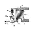
另外,在本实施方式中,图9表示使用面安装独立部件时的安装例。在本图中,表示了具有源电极11、漏电极12、和栅电极13的MOSFET 1,P型MOSFET 81a,二极管82,OFF用栅极电阻52的安装形态。如本图所示,可以以简单的构成来进行安装。另外,导通切换电路8也可以是在构成MOSFET 1的半导体芯片上形成电路而成的电路。在这种情况下,安装形态可以进一步简化。In addition, in this embodiment, FIG. 9 shows an example of mounting when using surface mounting of individual components. In this figure, a
实施方式2
在图7表示本发明的实施方式2的构成。FIG. 7 shows the configuration of
在将导通切换电路8中的二极管设为齐纳二极管来作为有源钳位电路的情况下,从齐纳二极管的电压范围的选定、温度特性和发热的问题出发,可以将齐纳二极管如齐纳二极管82a、82b那样设成多级。在该情况下,在区间t1即使使栅极-漏极间导通,由于齐纳二极管的顺方向电压也是多级,所以不能充分地放净栅极电荷。In the case where the diode in the
因此,如图7所示,和多级的齐纳二极管82a、82b并联地连接有旁路用二极管83,设定旁路用二极管83的逆向耐压比多级的齐纳二极管82a、82b的齐纳电压总和要大。通过采用这样的构成,可以在截止初期的区间t1中在旁路用二极管83的顺方向电压放电,在截止后期的区间t2中的有源钳位动作时,可以以齐纳二极管82a、82b的齐纳电压的总和来规定钳位电压。Therefore, as shown in FIG. 7, a bypass diode 83 is connected in parallel with the multistage Zener diodes 82a, 82b, and the reverse withstand voltage of the bypass diode 83 is set to be higher than that of the multistage Zener diodes 82a, 82b. The sum of the zener voltages should be large. By adopting such a configuration, the forward voltage of the bypass diode 83 can be discharged in the period t1 at the beginning of the turn-off period, and the voltage of the Zener diodes 82a and 82b can be used during the active clamp operation in the period t2 at the later period of the turnoff period. The sum of the zener voltages to specify the clamping voltage.
本实施方式的构成,特别是在浪涌能量较大的应用和驱动栅极输入电容较大的电压驱动型晶体管的情况下有效。The configuration of the present embodiment is particularly effective in the application of a large surge energy and in the case of driving a voltage-driven transistor with a large gate input capacitance.
实施方式3
在图8表示本发明的实施方式3的构成。FIG. 8 shows the configuration of
在本实施方式中,使用N型MOSFET 81b作为导通切换电路8的开关。另外,N型MOSFET 81b的栅电极由栅极OFF指令32驱动。栅极OFF指令32通过NOT电路71输入到N型MOSFET 81b的栅电极。本实施方式的构成,不依存于栅极OFF用开关42的状态,在可以独立控制N型MOSFET 81b的栅极电压的点上有利。In this embodiment, an N-
在上述的实施方式1、2中,P型MOSFET 81a的输入电容和OFF用栅极电阻52并联地连接,所以,可以带来与在栅极常数附加高通滤波器的情况相同的效果。因此,需要考虑P型MOSFET 81a的输入电容所带来的影响来设计栅极常数。In
与此相对,在本实施方式中,N型MOSFET 81b的反馈电容并联地连接,通常反馈电容相对于输入电容是十分小的值。因此,可以减小反馈电容的影响。即栅极常数的选择范围进一步扩大。On the other hand, in the present embodiment, the feedback capacitance of the N-
实施方式4
在图10表示本发明的实施方式4的构成。图10表示3相的逆变器系统100。FIG. 10 shows the configuration of
在逆变器系统100中,控制器65输出栅极驱动指令311、312、321、322、331、332。上支路(arm)的U相、V相、W相的MOSFET 111、121、131,以及下支路的U相、V相、W相的MOSFET 112、122、132分别根据控制器65输出的栅极驱动指令311、312、321、322、331、332,通过电压切换电路411、412、421、422、431、432,进行ON/OFF的开关控制。逆变器系统100通过MOSFET 111、112、121、122、131、132的开关动作,对电动机64输出U相、V相、W相的交流电流来驱动电动机。In the inverter system 100 , the
在串联连接的上支路和下支路之间,连接有蓄电池63,供给直流电。逆变器系统100将蓄电池63供给的直流电变换成3相的交流电。另外,由于在MOSFET 111、112、121、122、131、132的开关动作时电压变动平滑化,所以平滑电容器62和蓄电池63并联地连接。在含有平滑电容器62的线路上存在有主电路寄生电感61,所以,在各个MOSFET的开关动作时会产生浪涌电压。Between the upper branch and the lower branch connected in series, a
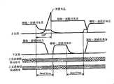
这里,在图12表示通过现有技术的固定电阻栅极驱动电路驱动逆变器系统时的上下支路的活动。为了抑制由主电路寄生电感61引起的浪涌电压,截止需要一定程度的时间。因此,需要调整栅极电阻。作为结果,截止时间(tOFF)也有增大的倾向。Here, FIG. 12 shows the activities of the upper and lower branches when the inverter system is driven by a conventional fixed resistance gate drive circuit. In order to suppress the surge voltage caused by the main circuit
另外,为了防止上下短路,直到上支路的截止时间(tOFF)结束为止,作为一支路的下支路不能为ON。因此,设置被称为空载时间(dead time)的上下支路的两方均为OFF的期间。In addition, in order to prevent short-circuiting up and down, the lower branch which is a branch cannot be turned ON until the off time (tOFF) of the upper branch ends. Therefore, a period called dead time (dead time) in which both the upper and lower branches are OFF is set.
若截止时间(tOFF)增大,则空载时间也需要较大地取值。其结果,在上下支路分别缩短了ON的时间。即电压利用效率变差,不能实现本来在控制器65希望的电压。If the cut-off time (tOFF) increases, the dead time also needs to take a larger value. As a result, the ON time is shortened in the upper and lower branches respectively. That is, the voltage utilization efficiency deteriorates, and the voltage originally desired by the
因此,在本实施方式的逆变器系统100中,分别在MOSFET 111、112、121、122、131、132,使用具有导通切换电路811、812、821、822、831、832的栅极驱动电路。Therefore, in the inverter system 100 of the present embodiment, gate drive circuits including
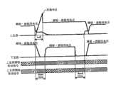
在图13表示在驱动具有这样的栅极驱动电路的逆变器系统时的上下支路的活动。即使将浪涌电压抑制到和现有技术相同的水平,也不会极端地缩短所述的区间t1。其结果,可以减小截止时间(tOFF)。因此,也可以减小空载时间,改善电压的利用率,可以接近控制器65的预期的理想的动作。FIG. 13 shows the movement of the upper and lower arms when driving an inverter system having such a gate drive circuit. Even if the surge voltage is suppressed to the same level as in the prior art, the above-mentioned interval t1 will not be extremely shortened. As a result, the off time (tOFF) can be reduced. Therefore, the dead time can also be reduced, the utilization rate of the voltage can be improved, and the expected ideal operation of the
如上所述,根据本实施方式的逆变器系统100,由于电流失真较少可以实现低噪声化以及平滑的控制动作。As described above, according to the inverter system 100 of the present embodiment, noise reduction and smooth control operation can be realized due to less current distortion.
实施方式5Embodiment 5
在图11表示本发明的实施方式5的构成。图11表示了DCDC变换器200。FIG. 11 shows the configuration of Embodiment 5 of the present invention. FIG. 11 shows a DCDC converter 200 .
DCDC变换器200的构成是在逆变器系统100中1相的构成中再加上电感69、平滑电容器67、和蓄电池68后的构成。The configuration of the DCDC converter 200 is a configuration in which an
DCDC变换器200与所述实施方式的逆变器系统100相比载波频率较高(数十到数百赫兹),需要尽量缩短截止时间(tOFF)。一般,载波频率变得越高,使用的电感69和变压器的体积可以越小。因此,通过采用本发明的构成,可以以更低成本实现高效率DCDC变换器。The DCDC converter 200 has a higher carrier frequency (tens to hundreds of hertz) than the inverter system 100 of the above-mentioned embodiment, and it is necessary to shorten the off time (tOFF) as much as possible. Generally, the higher the carrier frequency becomes, the smaller the size of the
以上对本发明的实施方式进行了具体的说明,但本发明并不限定于所述实施方式的内容,可以在不脱离本发明的技术思想的范围内进行各种变更。As mentioned above, although embodiment of this invention was concretely demonstrated, this invention is not limited to the content of the said embodiment, Various changes are possible in the range which does not deviate from the technical idea of this invention.
例如,在所述实施方式中,对使用MOSFET作为电压驱动型晶体管的情况进行了说明,也可以使用IGBT来代替MOSFET。在使用IGBT的情况下,MOSFET的源极相当于IGBT的发射极,MOSFET的漏极相当于IGBT的集电极。另外,虽然在MOSFET的构造上,回流用的二极管被内置,但在使用IGBT的情况需要将二极管外设。For example, in the above-described embodiments, a case where a MOSFET is used as a voltage-driven transistor has been described, but an IGBT may be used instead of a MOSFET. When using an IGBT, the source of the MOSFET corresponds to the emitter of the IGBT, and the drain of the MOSFET corresponds to the collector of the IGBT. In addition, in the structure of the MOSFET, a diode for return flow is built in, but when using an IGBT, the diode needs to be provided externally.
另外,漏极-源极间电压(Vds)和栅极-源极间电压(Vgs)的大小关系,和导通切换电路8的导通/非导通之间的关系,若能实际一致最好,但并不要求严格的一致。由于电路特性或其他理由,在必要的情况下,可以在不脱离本发明的宗旨的范围内适当地变更所述关系。因此,可以按照在漏极-源极间电压(Vds)和栅极-源极间电压(Vgs)的差比0以外的规定值(Va)小的情况下(Vds-Vgs<Va),导通切换电路8导通的方式控制,按照该差比规定值大的情况下(Vds-Vgs>Va)导通切换电路8非导通的方式控制。In addition, the relationship between the magnitude of the drain-source voltage (Vds) and the gate-source voltage (Vgs), and the relationship between conduction/non-conduction of the
以上,根据本发明的所述实施方式,在截止时的区间(t1),在栅电极13和源电极11之间充电的电荷与OFF用栅极电阻52无关,可以通过导通切换电路8和漏电极12放电。因此,可以极端地缩短区间(t1),并且,可以和区间(t1)的特性分离地选择抑制浪涌电压用的OFF用栅极电阻52的最合适的值。As described above, according to the above-described embodiment of the present invention, in the interval (t1) at the time of OFF, the charge charged between the
作为结果,由于截止时间缩短,可以实现提高电压利用率和减少电压失真。例如,在用于电动机驱动用的逆变器系统的情况下,可以实现平滑的电动机驱动和低噪声化。另外,在用于DCDC变换器的情况下,由于良好的控制性能以及载波频率得到提高,可以实现小型化、低成本化以及高效率化。As a result, improved voltage utilization and reduced voltage distortion can be achieved due to shortened off-time. For example, when used in an inverter system for driving a motor, smooth motor driving and noise reduction can be realized. In addition, when used in a DCDC converter, since the control performance is good and the carrier frequency is improved, miniaturization, cost reduction, and high efficiency can be achieved.
另外,即使在为了切断短路以及过电流而使栅极电阻增大的情况下,由于区间(t1)可以与栅极电阻不相关地缩短,所以可以将电流切断延迟降至最小,有防止由延迟部分引起的电流增加的效果。In addition, even when the gate resistance is increased to cut off a short circuit or an overcurrent, since the interval (t1) can be shortened independently of the gate resistance, the current cut-off delay can be minimized, preventing delays caused by The effect of the current increase caused by the part.
产业上的可利用性Industrial availability
本发明可以适用于存在抑制浪涌电压和缩短截止时间的双重需求的所有栅极驱动电路。特别是适用于混合动力汽车或电动车等的逆变器系统或DCDC变换器等。The present invention can be applied to all gate drive circuits that have dual demands of suppressing surge voltage and shortening turn-off time. In particular, it is suitable for inverter systems, DCDC converters, etc. of hybrid vehicles or electric vehicles.
Claims (13)
Translated fromChineseApplications Claiming Priority (2)
| Application Number | Priority Date | Filing Date | Title |
|---|---|---|---|
| JP2007167069AJP2009011013A (en) | 2007-06-26 | 2007-06-26 | Power converter |
| JP2007167069 | 2007-06-26 |
Publications (1)
| Publication Number | Publication Date |
|---|---|
| CN101335483Atrue CN101335483A (en) | 2008-12-31 |
Family
ID=39832223
Family Applications (1)
| Application Number | Title | Priority Date | Filing Date |
|---|---|---|---|
| CNA2008101288631APendingCN101335483A (en) | 2007-06-26 | 2008-06-20 | power conversion device |
Country Status (4)
| Country | Link |
|---|---|
| US (1) | US20090001410A1 (en) |
| EP (1) | EP2009775A2 (en) |
| JP (1) | JP2009011013A (en) |
| CN (1) | CN101335483A (en) |
Cited By (6)
| Publication number | Priority date | Publication date | Assignee | Title |
|---|---|---|---|---|
| CN102386799A (en)* | 2010-08-31 | 2012-03-21 | 日立汽车系统株式会社 | Power supply circuit and power conversion device |
| CN102403968A (en)* | 2010-08-27 | 2012-04-04 | 瑞萨电子株式会社 | Output circuit |
| CN102684541A (en)* | 2011-03-18 | 2012-09-19 | 三菱电机株式会社 | Inverter controller and refrigerating and air-conditioning unit |
| CN102957306A (en)* | 2011-08-19 | 2013-03-06 | 株式会社安川电机 | Gate drive circuit and power converter |
| CN107155387A (en)* | 2014-09-11 | 2017-09-12 | 三菱电机株式会社 | Semiconductor device |
| CN109314509A (en)* | 2016-06-17 | 2019-02-05 | 日产自动车株式会社 | Driving device |
Families Citing this family (6)
| Publication number | Priority date | Publication date | Assignee | Title |
|---|---|---|---|---|
| US7277782B2 (en)* | 2001-01-31 | 2007-10-02 | Oshkosh Truck Corporation | Control system and method for electric vehicle |
| JP5736243B2 (en)* | 2011-06-13 | 2015-06-17 | 本田技研工業株式会社 | Power circuit |
| JP6390515B2 (en)* | 2015-05-22 | 2018-09-19 | 株式会社デンソー | Switching speed setting method |
| JP6757637B2 (en)* | 2016-09-23 | 2020-09-23 | 株式会社ケーヒン | Inductive load drive |
| JP6953176B2 (en)* | 2017-05-18 | 2021-10-27 | キヤノン株式会社 | Power supply and image forming equipment |
| US12122251B2 (en)* | 2022-09-28 | 2024-10-22 | BorgWarner US Technologies LLC | Systems and methods for bidirectional message architecture for inverter for electric vehicle |
Family Cites Families (6)
| Publication number | Priority date | Publication date | Assignee | Title |
|---|---|---|---|---|
| JP3462032B2 (en)* | 1997-03-04 | 2003-11-05 | 株式会社東芝 | Power converter |
| JPH11178318A (en)* | 1997-12-04 | 1999-07-02 | Toshiba Corp | Drive circuit for voltage-driven power devices |
| JP3255147B2 (en) | 1998-06-19 | 2002-02-12 | 株式会社デンソー | Surge protection circuit for insulated gate transistor |
| JP3598933B2 (en)* | 2000-02-28 | 2004-12-08 | 株式会社日立製作所 | Power converter |
| JP2002369495A (en) | 2001-06-12 | 2002-12-20 | Nissan Motor Co Ltd | Drive circuit for voltage-driven elements |
| DK1801233T3 (en) | 2005-12-22 | 2010-02-08 | Siemens Healthcare Diagnostics | Diagnostic method for recognition of carriers of the Marburg I variant of the factor VII activating protease (FSAP) by differential modulation of FSAP activity |
- 2007
- 2007-06-26JPJP2007167069Apatent/JP2009011013A/enactivePending
- 2008
- 2008-06-20CNCNA2008101288631Apatent/CN101335483A/enactivePending
- 2008-06-24EPEP08011415Apatent/EP2009775A2/ennot_activeWithdrawn
- 2008-06-25USUS12/145,894patent/US20090001410A1/ennot_activeAbandoned
Cited By (10)
| Publication number | Priority date | Publication date | Assignee | Title |
|---|---|---|---|---|
| CN102403968A (en)* | 2010-08-27 | 2012-04-04 | 瑞萨电子株式会社 | Output circuit |
| CN102386799A (en)* | 2010-08-31 | 2012-03-21 | 日立汽车系统株式会社 | Power supply circuit and power conversion device |
| CN102386799B (en)* | 2010-08-31 | 2014-09-17 | 日立汽车系统株式会社 | Power supply circuit and power conversion device |
| CN102684541A (en)* | 2011-03-18 | 2012-09-19 | 三菱电机株式会社 | Inverter controller and refrigerating and air-conditioning unit |
| CN102684541B (en)* | 2011-03-18 | 2014-10-29 | 三菱电机株式会社 | Inverter controller and refrigerating and air-conditioning unit |
| CN102957306A (en)* | 2011-08-19 | 2013-03-06 | 株式会社安川电机 | Gate drive circuit and power converter |
| CN102957306B (en)* | 2011-08-19 | 2015-11-25 | 株式会社安川电机 | Gate driver circuit and power conversion unit |
| CN107155387A (en)* | 2014-09-11 | 2017-09-12 | 三菱电机株式会社 | Semiconductor device |
| CN109314509A (en)* | 2016-06-17 | 2019-02-05 | 日产自动车株式会社 | Driving device |
| CN109314509B (en)* | 2016-06-17 | 2020-03-10 | 日产自动车株式会社 | Drive device |
Also Published As
| Publication number | Publication date |
|---|---|
| JP2009011013A (en) | 2009-01-15 |
| EP2009775A2 (en) | 2008-12-31 |
| US20090001410A1 (en) | 2009-01-01 |
Similar Documents
| Publication | Publication Date | Title |
|---|---|---|
| CN101335483A (en) | power conversion device | |
| US8351231B2 (en) | Power conversion device | |
| US8810287B2 (en) | Driver for semiconductor switch element | |
| US20120268091A1 (en) | Switching circuit device and power supply device having same | |
| US9998110B2 (en) | System and method for variable impedance gate driver | |
| IL95438A (en) | Switching circuit | |
| KR20150140304A (en) | Commutation cell and compensation circuit therefor | |
| JP2003052178A (en) | Three-level inverter device | |
| JP2018520625A (en) | Power converter physical topology | |
| HK1232343A1 (en) | Gate driver controlling a collector to emitter voltage variation of an electronic switch and circuits including the gate driver | |
| KR100936427B1 (en) | Power converter | |
| JP2021013259A (en) | Gate drive and power converter | |
| CN105453434A (en) | Driver Unit Using Gallium Nitride Switches | |
| JP2019193406A (en) | Gate drive circuit and gate drive method | |
| JP6683950B2 (en) | Driving power supply device for voltage-driven semiconductor switching element and control method thereof | |
| JP2017220861A (en) | Gate drive circuit | |
| JP5382535B2 (en) | Power supply device for gate drive circuit | |
| JP4212546B2 (en) | Power converter | |
| JP2018088728A (en) | Gate drive circuit | |
| WO2023062745A1 (en) | Driving circuit for power semiconductor device, power semiconductor module, and power converter | |
| JP5832845B2 (en) | Semiconductor module and power conversion module | |
| Li et al. | Active gate current control for non-insulating-gate WBG devices | |
| JP6004988B2 (en) | Gate control device for power semiconductor device | |
| JPH10209832A (en) | Semiconductor switch circuit | |
| CN108141129B (en) | Power converter configured to limit switching overvoltage |
Legal Events
| Date | Code | Title | Description |
|---|---|---|---|
| C06 | Publication | ||
| PB01 | Publication | ||
| C10 | Entry into substantive examination | ||
| SE01 | Entry into force of request for substantive examination | ||
| C02 | Deemed withdrawal of patent application after publication (patent law 2001) | ||
| WD01 | Invention patent application deemed withdrawn after publication | Open date:20081231 |