CN101334565A - pixel unit - Google Patents
pixel unitDownload PDFInfo
- Publication number
- CN101334565A CN101334565ACNA2007101290336ACN200710129033ACN101334565ACN 101334565 ACN101334565 ACN 101334565ACN A2007101290336 ACNA2007101290336 ACN A2007101290336ACN 200710129033 ACN200710129033 ACN 200710129033ACN 101334565 ACN101334565 ACN 101334565A
- Authority
- CN
- China
- Prior art keywords
- disposed
- layer
- color filter
- pixel cell
- reflection type
- Prior art date
- Legal status (The legal status is an assumption and is not a legal conclusion. Google has not performed a legal analysis and makes no representation as to the accuracy of the status listed.)
- Pending
Links
- 239000000758substrateSubstances0.000claimsabstractdescription57
- 239000004973liquid crystal related substanceSubstances0.000claimsabstractdescription47
- 239000012788optical filmSubstances0.000claimsabstractdescription32
- 239000000463materialSubstances0.000claimsdescription16
- 230000000149penetrating effectEffects0.000claimsdescription15
- AMGQUBHHOARCQH-UHFFFAOYSA-Nindium;oxotinChemical compound[In].[Sn]=OAMGQUBHHOARCQH-UHFFFAOYSA-N0.000claimsdescription7
- VYZAMTAEIAYCRO-UHFFFAOYSA-NChromiumChemical compound[Cr]VYZAMTAEIAYCRO-UHFFFAOYSA-N0.000claimsdescription6
- 229910052581Si3N4Inorganic materials0.000claimsdescription6
- 229910052804chromiumInorganic materials0.000claimsdescription6
- 239000011651chromiumSubstances0.000claimsdescription6
- HQVNEWCFYHHQES-UHFFFAOYSA-Nsilicon nitrideChemical compoundN12[Si]34N5[Si]62N3[Si]51N64HQVNEWCFYHHQES-UHFFFAOYSA-N0.000claimsdescription6
- YVTHLONGBIQYBO-UHFFFAOYSA-Nzinc indium(3+) oxygen(2-)Chemical compound[O--].[Zn++].[In+3]YVTHLONGBIQYBO-UHFFFAOYSA-N0.000claimsdescription6
- 239000011248coating agentSubstances0.000claims36
- 238000000576coating methodMethods0.000claims36
- 239000010408filmSubstances0.000abstractdescription149
- 239000004642PolyimideSubstances0.000description7
- 229920001721polyimidePolymers0.000description7
- 239000012528membraneSubstances0.000description6
- 230000000694effectsEffects0.000description5
- 239000003086colorantSubstances0.000description4
- 238000004519manufacturing processMethods0.000description4
- 239000002861polymer materialSubstances0.000description4
- 229910052709silverInorganic materials0.000description4
- 239000004332silverSubstances0.000description4
- 229910000838Al alloyInorganic materials0.000description3
- VYPSYNLAJGMNEJ-UHFFFAOYSA-NSilicium dioxideChemical compoundO=[Si]=OVYPSYNLAJGMNEJ-UHFFFAOYSA-N0.000description3
- 238000010586diagramMethods0.000description3
- 229910052814silicon oxideInorganic materials0.000description3
- 239000004988Nematic liquid crystalSubstances0.000description2
- 238000010521absorption reactionMethods0.000description2
- 239000004020conductorSubstances0.000description2
- 239000003989dielectric materialSubstances0.000description2
- 238000000034methodMethods0.000description2
- 229910000583Nd alloyInorganic materials0.000description1
- UBSJOWMHLJZVDJ-UHFFFAOYSA-Naluminum neodymiumChemical compound[Al].[Nd]UBSJOWMHLJZVDJ-UHFFFAOYSA-N0.000description1
- 230000005540biological transmissionEffects0.000description1
- 238000012986modificationMethods0.000description1
- 230000004048modificationEffects0.000description1
- 230000035515penetrationEffects0.000description1
- 125000006850spacer groupChemical group0.000description1
Images


Landscapes
- Liquid Crystal (AREA)
Abstract
Description
Translated fromChinese技术领域technical field
本发明是有关于一种半透式液晶显示器及其像素单元,且特别是有关于一种能够兼顾色彩饱和度(color saturation)与亮度(brightness)的像素单元设计。The present invention relates to a transflective liquid crystal display and its pixel unit, and in particular to a pixel unit design capable of both color saturation and brightness.
背景技术Background technique
由于液晶显示器为非自发光的显示器,因此需要一个外加光源以提供液晶面板足够的亮度,依其光源的不同可分为穿透式液晶显示器、半穿透-半反射式液晶显示器与反射式液晶显示器三种。其中,穿透式液晶显示器利用背光模组以提供足够的光源,需要消耗较多的电力,而不适合应用于手机、个人数字助理(Personal Digital Assistant,PDA)和电子书(e-Book)等等携带型产品上。因此,为了改善液晶显示器耗电量高的问题,能够运用外界光源的半穿透-半反射式液晶显示器与反射式液晶显示器已逐渐受到各方嘱目。Since the liquid crystal display is a non-self-illuminating display, an external light source is needed to provide sufficient brightness for the liquid crystal panel. According to the different light sources, it can be divided into transmissive liquid crystal display, semi-transmissive-semi-reflective liquid crystal display and reflective liquid crystal display. Three types of displays. Among them, the transmissive liquid crystal display uses the backlight module to provide sufficient light source, which requires more power consumption, and is not suitable for mobile phones, personal digital assistants (Personal Digital Assistant, PDA) and e-books (e-Book), etc. And other portable products. Therefore, in order to improve the problem of high power consumption of liquid crystal displays, semi-transmissive-semi-reflective liquid crystal displays and reflective liquid crystal displays that can use external light sources have gradually attracted the attention of all parties.
图1为现有具有反射式显示模式的液晶显示器像素单元中反射区域的剖面示意图。一般而言,像素单元100包括共用电极112、彩色滤光层114、像素电极122、反射层124以及液晶层130。其中,共用电极112配置于上基板110上,像素电极122配置于下基板120上。像素电极122与反射层124配置于下基板120上,且反射层124是配置于像素单元100的像素电极122之下以使外界光线能够被反射以达到显示的效果(如图1中箭头所示)。此外,液晶层130则配置于共用电极112与像素电极122之间。为了呈现多彩显示效果,现有的像素单元100可进一步地搭配一配置于上基板110与共用电极112之间的彩色滤光层114。FIG. 1 is a schematic cross-sectional view of a reflective region in a pixel unit of a conventional liquid crystal display with a reflective display mode. In general, the
值得注意的是,由于彩色滤光层114会过滤掉部分的外界光源,仅允许具有特定波长范围的光线穿过彩色滤光层114,因此穿过彩色滤光层114的光线强度便大幅降低。为了提高像素单元100的显示亮度,可在彩色滤光层114上做开口设计,但此开口设计会使其显示影像的色彩饱和度降低。换言之,现有的像素结构100无法兼顾高亮度与高色彩饱和度的需求。It is worth noting that, since the
发明内容Contents of the invention
本发明提供一种像素单元,以兼顾像素单元的亮度以及色彩饱和度。The invention provides a pixel unit to take into account the brightness and color saturation of the pixel unit.
本发明提出一种像素单元,适于配置于一上基板与一下基板之间,其包括主动元件、反射式彩色滤光膜、共用电极以及液晶层。其中,主动元件配置于下基板上,而反射式彩色滤光膜也配置于下基板上,并且反射式彩色滤光膜与主动元件电性连接。此外,共用电极配置于上基板上,并且液晶层配置于反射式彩色滤光膜以及共用电极之间。值得注意的是,反射式彩色滤光膜包括反射膜、间隙层、半透膜以及透明光学膜。其中,间隙层配置于反射膜上,半透膜配置于间隙层上。此外,透明光学膜配置于半透膜上。The invention proposes a pixel unit, which is suitable for being disposed between an upper substrate and a lower substrate, and includes an active element, a reflective color filter film, a common electrode and a liquid crystal layer. Wherein, the active element is arranged on the lower substrate, and the reflective color filter film is also arranged on the lower substrate, and the reflective color filter film is electrically connected with the active element. In addition, the common electrode is disposed on the upper substrate, and the liquid crystal layer is disposed between the reflective color filter film and the common electrode. It is worth noting that the reflective color filter film includes reflective film, gap layer, semi-permeable film and transparent optical film. Wherein, the gap layer is configured on the reflective film, and the semi-permeable film is configured on the gap layer. In addition, the transparent optical film is disposed on the semi-permeable film.
本发明又提出一种像素单元,适于配置于一上基板与一下基板之间,其包括反射式彩色滤光膜、共用电极以及液晶层。其中,反射式彩色滤光膜也配置于下基板上。此外,共用电极配置于上基板上,并且液晶层配置于反射式彩色滤光膜以及共用电极之间。反射式彩色滤光膜包括反射膜、间隙层、半透膜以及透明光学膜。其中,间隙层配置于反射膜上,半透膜配置于间隙层上。此外,透明光学膜配置于半透膜上。The present invention further proposes a pixel unit, which is suitable for being disposed between an upper substrate and a lower substrate, and includes a reflective color filter film, a common electrode and a liquid crystal layer. Wherein, the reflective color filter film is also configured on the lower substrate. In addition, the common electrode is disposed on the upper substrate, and the liquid crystal layer is disposed between the reflective color filter film and the common electrode. The reflective color filter film includes reflective film, gap layer, semi-permeable film and transparent optical film. Wherein, the gap layer is configured on the reflective film, and the semi-permeable film is configured on the gap layer. In addition, the transparent optical film is disposed on the semi-permeable film.
在本发明的像素单元中,上述的反射膜的材质包括铝合金或是银,而间隙层的材质包括氮化硅或氧化硅,另外半透膜的材质例如是铬。此外,半透膜例如是与反射膜电性连接的。In the pixel unit of the present invention, the material of the reflective film includes aluminum alloy or silver, the material of the gap layer includes silicon nitride or silicon oxide, and the material of the semi-permeable film is, for example, chromium. In addition, the semi-permeable film is electrically connected with the reflective film, for example.
在本发明的像素单元中,上述的透明光学膜包括透明导电层,其材质例如是铟锡氧化物或铟锌氧化物。此外,透明导电层例如是由半透膜上延伸至半透膜之外,以于半透膜旁定义出一穿透区。如此,像素单元还可包括一垫高层,其配置于反射式彩色滤光膜上或是反射式彩色滤光膜与下基板之间。另外,还可在上基板上配置一彩色滤光层,使其位于穿透区上方。In the pixel unit of the present invention, the above-mentioned transparent optical film includes a transparent conductive layer made of, for example, indium tin oxide or indium zinc oxide. In addition, for example, the transparent conductive layer extends from the semi-permeable membrane to the outside of the semi-permeable membrane, so as to define a penetrating area beside the semi-permeable membrane. In this way, the pixel unit may further include a pad layer disposed on the reflective color filter film or between the reflective color filter film and the lower substrate. In addition, a color filter layer can also be arranged on the upper substrate so that it is located above the penetrating area.
在本发明的像素单元中,上述的透明光学膜的材质例如是聚醯亚胺。In the pixel unit of the present invention, the material of the transparent optical film is, for example, polyimide.
在本发明的像素单元中,上述的反射式彩色滤光膜还包括一透明电极(transparent electrode),配置于反射膜与下基板之间,透明电极与主动元件电性连接并且由反射膜下方延伸至反射膜之外,以于反射膜旁定义出一穿透区。In the pixel unit of the present invention, the above-mentioned reflective color filter film also includes a transparent electrode (transparent electrode), which is arranged between the reflective film and the lower substrate, and the transparent electrode is electrically connected to the active element and extends from the bottom of the reflective film to the outside of the reflective film to define a penetrating area beside the reflective film.
在本发明的像素单元中,像素单元中可进一步包括一垫高层,其配置位置例如是于反射式彩色滤光膜上或透明电极与下基板之间,又或是反射膜与透明电极之间。另一方面,当垫高层配置于反射膜与透明电极之间时,像素单元可进一步包括一位于垫高层中的导电接触孔,以使反射膜以及透明电极经由导电接触孔做电性连接。In the pixel unit of the present invention, the pixel unit may further include a pad layer, which is disposed, for example, on the reflective color filter film or between the transparent electrode and the lower substrate, or between the reflective film and the transparent electrode. . On the other hand, when the pad layer is disposed between the reflective film and the transparent electrode, the pixel unit may further include a conductive contact hole in the pad layer, so that the reflective film and the transparent electrode are electrically connected through the conductive contact hole.
除此之外,本发明另提出一种半透式液晶显示器的像素单元,其包括主动元件、反射式彩色滤光膜、穿透电极层(transmissive electrode)、共用电极以及液晶层。主动元件与反射式彩色滤光膜配置于下基板上,并且反射式彩色滤光膜与主动元件电性连接。另外,穿透电极层配置于下基板上,位于反射式彩色滤光膜的一侧,并且穿透电极层与反射式彩色滤光膜电性连接。共用电极配置于上基板上,而液晶层配置于反射式彩色滤光膜、穿透电极层以及共用电极之间。反射式彩色滤光膜包括反射膜、间隙层、半透膜以及透明光学膜。其中,间隙层配置于反射膜上,半透膜配置于间隙层上。此外,透明光学膜配置于半透膜上。In addition, the present invention further proposes a pixel unit of a transflective liquid crystal display, which includes an active element, a reflective color filter film, a transmissive electrode layer, a common electrode, and a liquid crystal layer. The active element and the reflective color filter film are arranged on the lower substrate, and the reflective color filter film is electrically connected with the active element. In addition, the penetrating electrode layer is disposed on the lower substrate, located on one side of the reflective color filter film, and electrically connected to the reflective color filter film. The common electrode is arranged on the upper substrate, and the liquid crystal layer is arranged between the reflective color filter film, the penetrating electrode layer and the common electrode. The reflective color filter film includes reflective film, gap layer, semi-permeable film and transparent optical film. Wherein, the gap layer is configured on the reflective film, and the semi-permeable film is configured on the gap layer. In addition, the transparent optical film is disposed on the semi-permeable film.
在本发明的像素单元中,上述的穿透电极层与反射式彩色滤光膜重叠部分为一反射区,穿透电极层未与反射式彩色滤光膜重叠部分为一穿透区。In the pixel unit of the present invention, the overlapping part of the transmissive electrode layer and the reflective color filter film is a reflective area, and the part of the transmissive electrode layer not overlapping with the reflective color filter film is a transmissive area.
在本发明的像素单元中,上述的半透膜与反射膜电性连接。In the pixel unit of the present invention, the above-mentioned semi-permeable film is electrically connected to the reflective film.
在本发明的像素单元中,像素单元可进一步包括一垫高层,此垫高层配置于反射式彩色滤光膜上或是反射式彩色滤光膜下。此外,半透膜例如是与反射膜电性连接的。In the pixel unit of the present invention, the pixel unit may further include a pad layer, and the pad layer is disposed on the reflective color filter film or under the reflective color filter film. In addition, the semi-permeable film is electrically connected with the reflective film, for example.
在本发明的像素单元中,像素单元可进一步包括配置于上基板上的彩色滤光层,其中彩色滤光层位于穿透电极层与上基板之间。In the pixel unit of the present invention, the pixel unit may further include a color filter layer disposed on the upper substrate, wherein the color filter layer is located between the penetrating electrode layer and the upper substrate.
本发明又提出一种像素单元,适于配置于上基板与下基板之间。此像素单元包括反射式彩色滤光膜、透明电极以及液晶层。反射式彩色滤光膜配置于下基板上,且反射式彩色滤光膜包括反射膜、间隙层、半透膜以及透明光学膜。间隙层配置于反射膜上,而半透膜配置于间隙层上。透明光学膜配置于半透膜上,且透明电极配置于上基板上。另外,液晶层配置于反射式彩色滤光膜以及透明电极之间。The present invention further provides a pixel unit suitable for being disposed between the upper substrate and the lower substrate. The pixel unit includes a reflective color filter film, a transparent electrode and a liquid crystal layer. The reflective color filter film is disposed on the lower substrate, and the reflective color filter film includes a reflective film, a gap layer, a semi-permeable film and a transparent optical film. The gap layer is configured on the reflective film, and the semi-permeable film is configured on the gap layer. The transparent optical film is arranged on the semi-permeable film, and the transparent electrode is arranged on the upper substrate. In addition, the liquid crystal layer is disposed between the reflective color filter film and the transparent electrode.
由于在本发明的像素单元中,被反射式彩色滤光膜反射后的光线具有特定的波长,并且被反射式彩色滤光膜反射的光线的波长与间隙层的膜厚相关。另一方面,在本发明的像素单元中,入射与反射的光线不需经过彩色滤光层,因此光线不会因彩色滤光层的吸收而减弱。因此,本发明的像素单元所显示的影像亮度较高,且具有不错的色彩饱和度。In the pixel unit of the present invention, the light reflected by the reflective color filter film has a specific wavelength, and the wavelength of the light reflected by the reflective color filter film is related to the film thickness of the gap layer. On the other hand, in the pixel unit of the present invention, the incident and reflected light does not need to pass through the color filter layer, so the light will not be weakened by the absorption of the color filter layer. Therefore, the image displayed by the pixel unit of the present invention has high brightness and good color saturation.
附图说明Description of drawings
为让本发明的上述目的、特征和优点能更明显易懂,以下结合附图对本发明的具体实施方式作详细说明,其中:In order to make the above-mentioned purposes, features and advantages of the present invention more obvious and understandable, the specific embodiments of the present invention will be described in detail below in conjunction with the accompanying drawings, wherein:
图1为现有像素单元中反射区域的剖面示意图。FIG. 1 is a schematic cross-sectional view of a reflective region in a conventional pixel unit.
图2A为本发明的第一实施例的一种像素单元的剖面示意图。FIG. 2A is a schematic cross-sectional view of a pixel unit according to the first embodiment of the present invention.
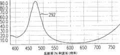
图2B到图2D为实际测量本发明的一实施例的反射式彩色滤光膜的不同色反射光的波长与反射率的关系图。FIG. 2B to FIG. 2D are diagrams showing the relationship between wavelengths and reflectances of different colors of reflected light of a reflective color filter film according to an embodiment of the present invention.
图2E到图2G为实际测量本发明的另一实施例的反射式彩色滤光膜的不同色反射光的波长与反射率的关系图。FIG. 2E to FIG. 2G are diagrams showing the relationship between the wavelength and the reflectance of the reflective color filter film of another embodiment of the present invention when the reflected light of different colors is actually measured.
图3A为本发明的第二实施例的一种像素单元的剖面示意图。3A is a schematic cross-sectional view of a pixel unit according to the second embodiment of the present invention.
图3B与图3C为两种可在像素单元300A的液晶层中形成不同单元间隙的结构示意图。FIG. 3B and FIG. 3C are schematic diagrams of two structures that can form different cell gaps in the liquid crystal layer of the
图4A为本发明的第三实施例的像素单元的剖面示意图。FIG. 4A is a schematic cross-sectional view of a pixel unit according to a third embodiment of the present invention.
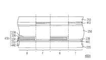
图4B到图4E绘示四种可使像素单元400A具有不同液晶层单元间隙的结构。FIG. 4B to FIG. 4E illustrate four structures that enable the
图5为本发明的第四实施例的像素单元的剖面示意图。FIG. 5 is a schematic cross-sectional view of a pixel unit according to a fourth embodiment of the present invention.
具体实施方式Detailed ways
为了使液晶显示器的显示效果能够有较佳的亮度以及高色彩饱和度,本发明提出一种具有反射式彩色滤光膜的像素单元。In order to make the display effect of the liquid crystal display have better brightness and high color saturation, the present invention proposes a pixel unit with a reflective color filter film.
第一实施例first embodiment
图2A为本发明的第一实施例的一种像素单元的剖面示意图。请参考图2A,上基板210与下基板220例如配置有像素单元200(本实施例中绘示出两个为例),且像素单元200包括主动元件(未绘示)、反射式彩色滤光膜230、共用电极240以及液晶层250。其中,主动元件(未绘示)配置于下基板220上,而反射式彩色滤光膜230也配置于下基板220上,并且反射式彩色滤光膜230与主动元件(未绘示)电性连接。此外,共用电极240配置于上基板210上,并且液晶层250配置于反射式彩色滤光膜230以及共用电极240之间。FIG. 2A is a schematic cross-sectional view of a pixel unit according to the first embodiment of the present invention. Please refer to FIG. 2A , the
反射式彩色滤光膜230包括反射膜232、间隙层234、半透膜236以及透明光学膜238。其中,间隙层234配置于反射膜232上,半透膜236配置于间隙层234上。此外,透明光学膜238配置于半透膜236上。为使提高显示品质,降低像素单元200内的阻抗值,半透膜236与反射膜232可以做电性连接。The reflective
在本实施例中,反射膜232的材质包括铝合金或是银,而间隙层234的材质包括氮化硅或氧化硅。半透膜236的材质例如是铬,而透明光学膜238的材质包括聚醯亚胺等高分子材质、铟锡氧化物、铟锌氧化物,或是其他透明导电材质。In this embodiment, the
在像素单元200中,反射式彩色滤光膜230中的半透膜236与反射膜232可分别使光线反射,而这些被反射的光线会产生干涉作用,换言之,经过反射式彩色滤光膜230处理后的光线会具有特定的波长,而此特定的波长与间隙层234的膜厚相关。In the
由实际经验得知,以铝-钕合金(AlNd)为反射膜232,氮化硅为间隙层234,铬为半透膜236,且铟锡氧化物(ITO)为透明光学膜238为例,欲使反射式彩色滤光膜230反射出蓝色光、绿色光及红色光时,间隙层234的膜厚则分别可以设计为208纳米、225纳米及162纳米。此时,蓝色光、绿色光及红色光的波长与反射率的关系则分别如图2B、图2C及图2D中的282、284及286所示。According to practical experience, taking aluminum-neodymium alloy (AlNd) as the
另外,若以银为反射膜232,氮化硅为间隙层234,铬为半透膜236,且聚醯亚胺为透明光学膜238时,欲反射出蓝色、绿色及红色的光,则间隙层234的膜厚例如各别为202纳米、223纳米及150纳米。其中,各色光的波长与反射率间的关系则分别如图2E、图2F及图2G中的292、294及296所示。In addition, if silver is used as the
综上所述,在相同的反射膜232、间隙层234、半透膜236及透明光学膜238材料结构下,借由调整间隙层234的膜厚,像素单元200可进行不同的色彩显示,其例如是红色、绿色及蓝色。自图2B到图2D中可发现各色光的反射率皆可高于70%,而在图2E到图2G中,各色光的反射率甚至皆超过90%。扼要地说,像素单元200则可兼顾高亮度以及高色彩饱和度的显示需求。另外,本发明的像素单元200也可以不包括主动元件,而为一被动式的像素单元200。换句话说,像素单元200例如可应用于超扭转向列型液晶显示器(Super TwistedNematic liquid Crystal display,STN-LCD)或是扭转向列型液晶显示器(TwistedNematic liquid Crystal display,TN-LCD)当中。To sum up, under the same material structure of the
第二实施例second embodiment
图3A为本发明的第二实施例的一种像素单元的剖面示意图。请参考图3A,像素单元300A与像素单元200相似,二者主要差异之处在于:像素单元300A中,反射式彩色滤光膜330是利用一透明导电层338作为透明光学膜之用,且透明导电层338例如是由半透膜236上延伸至半透膜236之外,以于半透膜236旁定义出一穿透区T。同时,像素单元300A中的反射膜232则定义出一反射区R。因此,像素单元300A是一种半穿透-半反射式像素单元。在本实施例中,透明导电层338的材质例如是铟锡氧化物或铟锌氧化物。3A is a schematic cross-sectional view of a pixel unit according to the second embodiment of the present invention. Please refer to FIG. 3A, the
在图3A中,像素单元300A可进一步包括一配置于上基板210上的彩色滤光层312,而彩色滤光层312是穿透区T内。彩色滤光层312例如是红色、绿色或蓝色等不同色彩的彩色滤光层。此时,像素单元300A在反射模式与穿透模式下皆可进行多彩化显示。In FIG. 3A , the
像素单元300A具有单一的液晶间隙(Cell gap),而以下提出两种可在像素单元300A的液晶层中形成双重液晶间隙的结构,如图3B与图3C所示。The
请先同时参考图3A与图3B,像素单元300B与像素单元300A相似。不过,像素单元300B还包括一垫高层360配置于反射式彩色滤光膜330之上。其中,垫高层360的材质例如是透明的介电材质。Please refer to FIG. 3A and FIG. 3B at the same time, the
另外,请同时参考图3A与图3C,像素单元300C的设计是源自像素单元300A的。只是,像素单元300C中,进一步配置垫高层360于反射式彩色滤光膜330之下。此时,垫高层360的作用在于使液晶层250具有双重间隙。实质上,为了进一步调整液晶层250中液晶分子的排列,本发明还可以在像素单元300A、300B、300C的下基板220上配置一覆盖在透明导电层338的上的配向膜层(未绘示)。In addition, please refer to FIG. 3A and FIG. 3C at the same time, the design of the
第三实施例third embodiment
图4A为本发明的第三实施例的像素单元的剖面示意图。请参考图4A,像素单元400A的设计是与像素单元200相似的。具体而言,像素单元400A还包括一透明电极440,配置于反射式彩色滤光膜430的反射膜232与下基板220之间。透明电极440与主动元件(未绘示)电性连接并且透明电极440例如是由反射膜232下方延伸至反射膜232之外。FIG. 4A is a schematic cross-sectional view of a pixel unit according to a third embodiment of the present invention. Please refer to FIG. 4A , the design of the
如图4A所示,透明电极440于反射膜232旁定义出一穿透区T,而反射膜232则定义出反射区R。因此,像素单元400A为一半穿透-半反射式像素单元。为了使像素单元400A具有更好的显示品质,还可在上基板210上配置一彩色滤光层412,并对应于穿透区T中。As shown in FIG. 4A , the
在本实施例中,透明光学膜238的材质例如为透明高分子材质,其包括聚醯亚胺。同时,透明光学膜238例如可自半透膜236上向外延伸至透明电极440上(如图4A所示)。另外,当透明光学膜238为聚醯亚胺时,可直接作为下配向膜层。在这样的设计之下,可以节省另外制作下配向膜层的流程与成本。在其他实施例中,透明光学膜238的材质也可以是透明导电材质,例如是铟锡氧化物或是铟锌氧化物等。In this embodiment, the material of the transparent
像素单元400A具有如像素单元200的优点,也就是说,像素单元400A可以呈现高亮度且高色饱和度的显示品质。The
以下更提出数种实施方式,借由配置一透明介电材质的垫高层460,以使像素单元400A具有双重液晶间隙,如图4B到图4E所绘示。请先参考图4B,像素单元400B还包括一垫高层460配置于反射式彩色滤光膜430之上。另外,如图4C所示,像素单元400C中将垫高层460配置于反射式彩色滤光膜430与下基板220之间。此外,像素单元400D的设计中,还可以将垫高层460配置于反射膜232与透明电极440之间(如图4D所示)。Several implementations are further proposed below, by disposing a
借由垫高层460的设计,使液晶层250具有双重液晶间隙,而可使像素单元(400B、400C及400D)具有更好的显示品质。Through the design of the
接着,请参照图4E,当垫高层460配置于反射膜232与透明电极440之间时,像素单元400E可更进一步包括一导电接触孔462配置于垫高层460中。配置导电接触孔462于垫高层460中,可使反射膜232及透明电极440之间电性连接,以避免反射膜232与半透膜236浮置所造成的问题,可进一步地维护像素单元400E的品质与寿命。Next, please refer to FIG. 4E , when the
第四实施例Fourth embodiment
本发明更提出一种半穿透-半反射式像素单元,如图5的像素单元500。图5为本发明的第四实施例的像素单元的剖面示意图。请参考图5,像素单元500适于配置于上基板510与下基板520之间,其包括主动元件(未绘示)、反射式彩色滤光膜530、穿透电极层522、共用电极540以及液晶层550。The present invention further proposes a semi-transmissive-semi-reflective pixel unit, such as the
像素单元500中,主动元件(未绘示)与反射式彩色滤光膜530配置于下基板520上,并且反射式彩色滤光膜530与主动元件(未绘示)电性连接。另外,穿透电极层522配置于下基板520上,并位于反射式彩色滤光膜530的一侧,且穿透电极层522与反射式彩色滤光膜530电性连接。此外,共用电极540配置于上基板510上,而液晶层550配置于下基板520的反射式彩色滤光膜530、穿透电极层522以及上基板510的共用电极540之间。In the
反射式彩色滤光膜530包括反射膜532、间隙层534、半透膜536以及透明光学膜538。其中,间隙层534配置于反射膜532上,半透膜536配置于间隙层534上并且半透膜536与反射膜532电性连接。此外,透明光学膜538配置于半透膜536上。反射式彩色滤光膜530的设计可使像素单元500有良好的显示品质。The reflective
在像素单元500中,穿透电极层522于反射式彩色滤光膜530的一侧定义出穿透区T,而反射式彩色滤光膜530所配置的区域则定义出反射区R。如此一来,像素单元500为半穿透-半反射式像素单元。In the
如图5所示,为了进一步提升像素单元500的显示效果,像素单元500更可包括一配置于上基板510上的彩色滤光层512,并且彩色滤光层512对应于穿透电极层522之上。另外,在其他实施例中,像素单元500还可以包括一垫高层(未绘示),配置于反射式彩色滤光膜530上或是反射式彩色滤光膜530下。As shown in FIG. 5 , in order to further improve the display effect of the
在一实施例中,反射膜532的材质例如是铝合金或是银,间隙层534的材质例如是氮化硅或是氧化硅,而半透膜536的材质例如是铬。另外,透明光学膜538的材质例如是聚醯亚胺、铟锡氧化物或铟锌氧化物。In one embodiment, the
当透明光学膜538的材质为聚醯亚胺或是其他高分子材质时,可于其接触液晶层550的一面形成配向膜功能。同时,可将透明光学膜538由半透膜536上向外延伸至穿透电极层522之上,以作为配向膜层之用,而有助于减化制造流程及生产成本。When the material of the transparent
综上所述,本发明的像素单元至少具有以下所述的优点:To sum up, the pixel unit of the present invention has at least the following advantages:
(1)本发明的像素单元中,反射式彩色滤光膜的设计可使光线产生干涉作用,而让像素单元进行多彩化的影像显示。(1) In the pixel unit of the present invention, the design of the reflective color filter film can cause interference of light, so that the pixel unit can display colorful images.
(2)本发明的像素单元在反射式模式显示下,光线不会因反复受到彩色滤光层的吸收而减弱,进而使像素单元所显示的影像有较佳的亮度。(2) When the pixel unit of the present invention is displayed in reflective mode, the light will not be weakened by repeated absorption by the color filter layer, so that the image displayed by the pixel unit has better brightness.
(3)由实际经验得知,本发明的像素单元能够呈现高亮度与较佳色彩饱和度的显示效果。(3) It is known from practical experience that the pixel unit of the present invention can display display effects with high brightness and better color saturation.
(4)本发明的像素单元的部分实施例中,透明光学膜以高分子材质制作时,可同时具有配向层的功用,而不需另制作配向膜层,进而简化制造流程。(4) In some embodiments of the pixel unit of the present invention, when the transparent optical film is made of polymer material, it can also function as an alignment layer, without the need to make an additional alignment film layer, thereby simplifying the manufacturing process.
(5)本发明的像素单元的部分实施例中,可借由不同的设计以于反射式彩色滤光膜旁定义出穿透区,而形成一半穿透-半反射式像素单元。(5) In some embodiments of the pixel unit of the present invention, different designs can be used to define a transmissive area next to the reflective color filter film to form a semi-transmissive-semi-reflective pixel unit.
(6)本发明的像素单元的部分实施例中,借由垫高层的设计可使液晶层具有双重的液晶间隙,而使像素单元具有更优越的显示品质。(6) In some embodiments of the pixel unit of the present invention, the liquid crystal layer has double liquid crystal gaps through the design of the pad layer, so that the pixel unit has better display quality.
虽然本发明已以较佳实施例揭示如上,然其并非用以限定本发明,任何本领域技术人员,在不脱离本发明的精神和范围内,当可作些许的修改和完善,因此本发明的保护范围当以权利要求书所界定的为准。Although the present invention has been disclosed above with preferred embodiments, it is not intended to limit the present invention. Any person skilled in the art may make some modifications and improvements without departing from the spirit and scope of the present invention. Therefore, the present invention The scope of protection should be defined by the claims.
Claims (23)
Priority Applications (1)
| Application Number | Priority Date | Filing Date | Title |
|---|---|---|---|
| CNA2007101290336ACN101334565A (en) | 2007-06-29 | 2007-06-29 | pixel unit |
Applications Claiming Priority (1)
| Application Number | Priority Date | Filing Date | Title |
|---|---|---|---|
| CNA2007101290336ACN101334565A (en) | 2007-06-29 | 2007-06-29 | pixel unit |
Publications (1)
| Publication Number | Publication Date |
|---|---|
| CN101334565Atrue CN101334565A (en) | 2008-12-31 |
Family
ID=40197250
Family Applications (1)
| Application Number | Title | Priority Date | Filing Date |
|---|---|---|---|
| CNA2007101290336APendingCN101334565A (en) | 2007-06-29 | 2007-06-29 | pixel unit |
Country Status (1)
| Country | Link |
|---|---|
| CN (1) | CN101334565A (en) |
Cited By (3)
| Publication number | Priority date | Publication date | Assignee | Title |
|---|---|---|---|---|
| CN103033976A (en)* | 2012-12-14 | 2013-04-10 | 京东方科技集团股份有限公司 | Liquid crystal display panel and display |
| WO2020220526A1 (en)* | 2019-04-30 | 2020-11-05 | 深圳市华星光电技术有限公司 | Reflective liquid crystal display panel |
| CN118655726A (en)* | 2024-07-11 | 2024-09-17 | 亚创光电(深圳)有限公司 | A high color gamut liquid crystal display screen |
- 2007
- 2007-06-29CNCNA2007101290336Apatent/CN101334565A/enactivePending
Cited By (4)
| Publication number | Priority date | Publication date | Assignee | Title |
|---|---|---|---|---|
| CN103033976A (en)* | 2012-12-14 | 2013-04-10 | 京东方科技集团股份有限公司 | Liquid crystal display panel and display |
| CN103033976B (en)* | 2012-12-14 | 2015-07-08 | 京东方科技集团股份有限公司 | Liquid crystal display panel and display |
| WO2020220526A1 (en)* | 2019-04-30 | 2020-11-05 | 深圳市华星光电技术有限公司 | Reflective liquid crystal display panel |
| CN118655726A (en)* | 2024-07-11 | 2024-09-17 | 亚创光电(深圳)有限公司 | A high color gamut liquid crystal display screen |
Similar Documents
| Publication | Publication Date | Title |
|---|---|---|
| TW562962B (en) | Liquid crystal display device | |
| US6697135B1 (en) | Transflective liquid crystal display device having reflective and transmissive mode parity | |
| KR100816145B1 (en) | Liquid crystal device and electronic apparatus | |
| US6806934B2 (en) | Transflective liquid crystal display having dielectric multilayer in LCD cells | |
| CN100573882C (en) | Thin-film transistor display panel | |
| CN101055386A (en) | image display system | |
| JP4813164B2 (en) | Thin film transistor display panel and liquid crystal display device including the same | |
| US20050128390A1 (en) | Transflective fringe field switching liquid crystal display | |
| WO2022007154A1 (en) | Liquid crystal display panel | |
| US20050128389A1 (en) | Transflective fringe field switching liquid crystal display | |
| CN100406977C (en) | Semi-penetration and semi-reflection type liquid crystal display | |
| WO2022007197A1 (en) | Liquid crystal display panel | |
| US20200004072A1 (en) | Touch panel and method for manufacturing the same | |
| WO2019029036A1 (en) | Transflective liquid crystal display | |
| CN202033561U (en) | Transflective pixel structure and transflective liquid crystal display | |
| JP2007226245A (en) | Liquid crystal display | |
| CN101334565A (en) | pixel unit | |
| JP4107047B2 (en) | Transflective liquid crystal display device | |
| TW200301833A (en) | Liquid crystal display device | |
| JP2009036800A (en) | Transflective liquid crystal display panel and electronic device | |
| US7369194B2 (en) | Fringe field switching liquid crystal display | |
| US20040001171A1 (en) | Partially light-penetrative and partially light-reflective LCD structure | |
| US20190056622A1 (en) | Transflective liquid crystal display and manufacturing method thereof | |
| JP2004212593A (en) | Liquid crystal display | |
| US20050140902A1 (en) | In plane switching liquid crystal display with transflector |
Legal Events
| Date | Code | Title | Description |
|---|---|---|---|
| C06 | Publication | ||
| PB01 | Publication | ||
| C10 | Entry into substantive examination | ||
| SE01 | Entry into force of request for substantive examination | ||
| C02 | Deemed withdrawal of patent application after publication (patent law 2001) | ||
| WD01 | Invention patent application deemed withdrawn after publication | Open date:20081231 |