CN101330044A - Substrate surface cleaning method, thin film manufacturing method, semiconductor device and manufacturing method thereof - Google Patents
Substrate surface cleaning method, thin film manufacturing method, semiconductor device and manufacturing method thereofDownload PDFInfo
- Publication number
- CN101330044A CN101330044ACNA200810125094XACN200810125094ACN101330044ACN 101330044 ACN101330044 ACN 101330044ACN A200810125094X ACNA200810125094X ACN A200810125094XACN 200810125094 ACN200810125094 ACN 200810125094ACN 101330044 ACN101330044 ACN 101330044A
- Authority
- CN
- China
- Prior art keywords
- gas
- film
- thin film
- vacuum chamber
- processed
- Prior art date
- Legal status (The legal status is an assumption and is not a legal conclusion. Google has not performed a legal analysis and makes no representation as to the accuracy of the status listed.)
- Granted
Links
- 238000000034methodMethods0.000titleclaimsabstractdescription77
- 239000010409thin filmSubstances0.000titleclaimsabstractdescription67
- 238000004519manufacturing processMethods0.000titleclaimsabstractdescription27
- 239000000758substrateSubstances0.000titleabstractdescription46
- 239000004065semiconductorSubstances0.000titleabstractdescription41
- 238000004140cleaningMethods0.000titleabstractdescription29
- 239000007789gasSubstances0.000claimsabstractdescription227
- 239000010408filmSubstances0.000claimsabstractdescription111
- 229910052751metalInorganic materials0.000claimsabstractdescription51
- 239000002184metalSubstances0.000claimsabstractdescription51
- 239000002994raw materialSubstances0.000claimsabstractdescription42
- 239000000126substanceSubstances0.000claimsabstractdescription19
- 229910052739hydrogenInorganic materials0.000claimsabstractdescription17
- 239000001257hydrogenSubstances0.000claimsabstractdescription13
- 239000000203mixtureSubstances0.000claimsabstractdescription10
- UFHFLCQGNIYNRP-UHFFFAOYSA-NHydrogenChemical compound[H][H]UFHFLCQGNIYNRP-UHFFFAOYSA-N0.000claimsabstractdescription8
- 230000008569processEffects0.000claimsdescription20
- 150000002902organometallic compoundsChemical class0.000claimsdescription6
- 125000002147dimethylamino groupChemical group[H]C([H])([H])N(*)C([H])([H])[H]0.000claims1
- 239000003054catalystSubstances0.000abstractdescription39
- 238000010438heat treatmentMethods0.000abstractdescription18
- 230000004888barrier functionEffects0.000abstractdescription12
- 238000005516engineering processMethods0.000abstractdescription8
- 230000015572biosynthetic processEffects0.000abstractdescription6
- 150000002222fluorine compoundsChemical class0.000abstractdescription4
- 150000001247metal acetylidesChemical class0.000abstractdescription3
- 150000004767nitridesChemical class0.000abstract1
- 239000010949copperSubstances0.000description39
- RYGMFSIKBFXOCR-UHFFFAOYSA-NCopperChemical compound[Cu]RYGMFSIKBFXOCR-UHFFFAOYSA-N0.000description24
- 229910052802copperInorganic materials0.000description24
- 150000002500ionsChemical class0.000description11
- 125000004435hydrogen atomChemical group[H]*0.000description9
- 239000012535impuritySubstances0.000description9
- 238000001020plasma etchingMethods0.000description9
- 229910052710siliconInorganic materials0.000description9
- OKTJSMMVPCPJKN-UHFFFAOYSA-NCarbonChemical compound[C]OKTJSMMVPCPJKN-UHFFFAOYSA-N0.000description7
- 229910052799carbonInorganic materials0.000description7
- 238000005229chemical vapour depositionMethods0.000description6
- 239000011148porous materialSubstances0.000description6
- 238000002230thermal chemical vapour depositionMethods0.000description6
- XUIMIQQOPSSXEZ-UHFFFAOYSA-NSiliconChemical compound[Si]XUIMIQQOPSSXEZ-UHFFFAOYSA-N0.000description5
- 238000004458analytical methodMethods0.000description5
- 239000000463materialSubstances0.000description5
- 238000005259measurementMethods0.000description5
- 238000006722reduction reactionMethods0.000description5
- 239000010703siliconSubstances0.000description5
- QPLDLSVMHZLSFG-UHFFFAOYSA-NCopper oxideChemical compound[Cu]=OQPLDLSVMHZLSFG-UHFFFAOYSA-N0.000description4
- 239000005751Copper oxideSubstances0.000description4
- ATJFFYVFTNAWJD-UHFFFAOYSA-NTinChemical compound[Sn]ATJFFYVFTNAWJD-UHFFFAOYSA-N0.000description4
- 229910052782aluminiumInorganic materials0.000description4
- 230000003197catalytic effectEffects0.000description4
- 229910000431copper oxideInorganic materials0.000description4
- 230000007423decreaseEffects0.000description4
- 230000000694effectsEffects0.000description4
- -1hydrogen ionsChemical class0.000description4
- 229910052718tinInorganic materials0.000description4
- WFKWXMTUELFFGS-UHFFFAOYSA-NtungstenChemical compound[W]WFKWXMTUELFFGS-UHFFFAOYSA-N0.000description4
- 230000000052comparative effectEffects0.000description3
- 238000000354decomposition reactionMethods0.000description3
- 238000009792diffusion processMethods0.000description3
- 238000005530etchingMethods0.000description3
- 238000009616inductively coupled plasmaMethods0.000description3
- 238000004544sputter depositionMethods0.000description3
- 238000003852thin film production methodMethods0.000description3
- PXGOKWXKJXAPGV-UHFFFAOYSA-NFluorineChemical compoundFFPXGOKWXKJXAPGV-UHFFFAOYSA-N0.000description2
- QVGXLLKOCUKJST-UHFFFAOYSA-Natomic oxygenChemical compound[O]QVGXLLKOCUKJST-UHFFFAOYSA-N0.000description2
- 239000012159carrier gasSubstances0.000description2
- 230000008859changeEffects0.000description2
- 239000013078crystalSubstances0.000description2
- 238000010586diagramMethods0.000description2
- 229910052731fluorineInorganic materials0.000description2
- 239000011737fluorineSubstances0.000description2
- 230000005596ionic collisionsEffects0.000description2
- 229910001512metal fluorideInorganic materials0.000description2
- 229910044991metal oxideInorganic materials0.000description2
- 150000004706metal oxidesChemical class0.000description2
- 230000007935neutral effectEffects0.000description2
- 125000002524organometallic groupChemical group0.000description2
- 239000001301oxygenSubstances0.000description2
- 229910052760oxygenInorganic materials0.000description2
- 230000009257reactivityEffects0.000description2
- 238000002310reflectometryMethods0.000description2
- 229910052715tantalumInorganic materials0.000description2
- 229910052721tungstenInorganic materials0.000description2
- RTAQQCXQSZGOHL-UHFFFAOYSA-NTitaniumChemical compound[Ti]RTAQQCXQSZGOHL-UHFFFAOYSA-N0.000description1
- XAGFODPZIPBFFR-UHFFFAOYSA-NaluminiumChemical compound[Al]XAGFODPZIPBFFR-UHFFFAOYSA-N0.000description1
- 125000004429atomChemical group0.000description1
- 230000008901benefitEffects0.000description1
- 230000000903blocking effectEffects0.000description1
- 230000005587bubblingEffects0.000description1
- 238000006243chemical reactionMethods0.000description1
- 230000003749cleanlinessEffects0.000description1
- 239000000470constituentSubstances0.000description1
- 238000007796conventional methodMethods0.000description1
- 230000005611electricityEffects0.000description1
- 235000011194food seasoning agentNutrition0.000description1
- 239000012212insulatorSubstances0.000description1
- 230000001678irradiating effectEffects0.000description1
- 238000000465mouldingMethods0.000description1
- 238000005268plasma chemical vapour depositionMethods0.000description1
- 238000007781pre-processingMethods0.000description1
- 239000012495reaction gasSubstances0.000description1
- 230000009467reductionEffects0.000description1
- 230000007261regionalizationEffects0.000description1
- 235000015067saucesNutrition0.000description1
- 230000001568sexual effectEffects0.000description1
- 238000000992sputter etchingMethods0.000description1
- 238000005728strengtheningMethods0.000description1
- 238000004381surface treatmentMethods0.000description1
- 239000010936titaniumSubstances0.000description1
- 229910052719titaniumInorganic materials0.000description1
- 238000009489vacuum treatmentMethods0.000description1
- 239000012808vapor phaseSubstances0.000description1
Images


Landscapes
- Chemical Vapour Deposition (AREA)
- Electrodes Of Semiconductors (AREA)
- Internal Circuitry In Semiconductor Integrated Circuit Devices (AREA)
Abstract
Translated fromChinese
Description
Translated fromChinese本申请是下述申请的分案申请:This application is a divisional application of:
申请号:200410095762.0Application number: 200410095762.0
申请日:2004年11月19日Application date: November 19, 2004
发明名称:衬底表面清洗方法、薄膜制造方法、半导体装置及其制法Title of Invention: Substrate surface cleaning method, thin film manufacturing method, semiconductor device and its manufacturing method
技术领域technical field
本发明的第一方面涉及一种薄膜形成技术,特别是涉及低温形成金属阻障膜的技术。The first aspect of the present invention relates to a thin film forming technology, in particular to the technology of forming a metal barrier film at low temperature.
本发明的第二方面涉及一种半导体装置中的金属膜的成膜方法,特别是涉及一种在金属表面或者Si表面上形成金属膜之前的清洗技术。The second aspect of the present invention relates to a method for forming a metal film in a semiconductor device, in particular to a cleaning technique before forming a metal film on a metal surface or a Si surface.
背景技术Background technique
(第一方面)(first)
为了在半导体衬底表面上形成薄膜,通常使用CVD(Chemical VaporDeposition)装置或者溅射(Sputtering)装置。In order to form a thin film on the surface of a semiconductor substrate, a CVD (Chemical Vapor Deposition) device or a sputtering (Sputtering) device is generally used.
以等离子体CVD法为例说明传统的薄膜制造方法时,图15中的符号101表示传统的CVD装置。When explaining a conventional thin film manufacturing method using the plasma CVD method as an example, reference numeral 101 in FIG. 15 denotes a conventional CVD apparatus.
参照该图,该CVD装置101有真空室120,该真空室120内部的底壁上设有加热板121,其内部顶棚附近设有高频电极122。Referring to this figure, the CVD apparatus 101 has a
加热板121上有提升杆(lift pin)124插入并通过,通过操作该提升杆124,将被处理物置放在加热板121上。图15中的符号102表示该状态下的被处理物。该被处理物102由加热板121内的加热器加热。A lifting pin (lift pin) 124 is inserted and passed through on the heating plate 121, and by operating the lifting pin 124, the object to be processed is placed on the heating plate 121. Reference numeral 102 in FIG. 15 represents the object to be processed in this state. The object to be processed 102 is heated by a heater inside the heating plate 121 .
高频电极122上连接有原料气体导入系统127与高频电源126。高频电极122的底面设有喷嘴123,从原料气体导入系统127提供给高频电极122的原料气体通过喷嘴123分散在真空室120内。A raw material gas introduction system 127 and a high-frequency power source 126 are connected to the high-frequency electrode 122 . Nozzles 123 are provided on the bottom of the high-frequency electrode 122 , and the source gas supplied to the high-frequency electrode 122 from the source gas introduction system 127 is dispersed in the
这种状态下,自高频电源126提供高频电压到高频电极122上,发生原料气体的等离子体,并在半导体衬底表面的Si或金属上形成薄膜。In this state, a high-frequency voltage is supplied from a high-frequency power supply 126 to the high-frequency electrode 122 to generate plasma of the raw material gas and form a thin film on Si or metal on the surface of the semiconductor substrate.
但是,在上述成形方法中,需要将被处理物加热到高温,因此不能满足近年的低温化工艺要求。However, in the above-mentioned molding method, it is necessary to heat the object to be processed to a high temperature, so it cannot meet the demands of the low-temperature process in recent years.
虽然现有技术中也研究过低温状态下的薄膜形成方法,但是形成金属布线或金属阻障膜时,会出现所得到薄膜的电阻率偏高的缺点(例如,参照特开2000-269163号公报)。Although the thin film formation method under the low temperature state has also been studied in the prior art, when forming metal wiring or metal barrier film, the shortcoming that the resistivity of the obtained thin film can appear on the high side (for example, refer to Japanese Patent Application Laid-Open No. 2000-269163 ).
并且,被处理物半导体衬底上的部分位置露出Cu膜时,其表面上会残留氧化铜、在前蚀刻工序中附着的氟(F)成分、碳(C)成分等,因此若以这种状态在Cu膜表面上形成金属阻障膜,则不能在金属阻障膜与Cu之间采用欧姆接触。Moreover, when the Cu film is exposed at a part of the semiconductor substrate to be processed, copper oxide, fluorine (F) components, carbon (C) components, etc. attached in the pre-etching step will remain on the surface. If a metal barrier film is formed on the surface of the Cu film, an ohmic contact cannot be used between the metal barrier film and Cu.
还有,传统技术的Cu膜表面的清洗工序中,通过向真空室内导入氢气并施加RF等高频来进行等离子化,并利用激励的氢离子除去Cu表面的氧化物、F成分、C成分等绝缘物。被处理物Cu膜的表面置于细孔(Via Hole)的下方,近年的典型的细孔,例如其孔径0.13μm、孔深0.85μm左右,且深宽比(aspect ratio)在5以上。In addition, in the cleaning process of the surface of the Cu film in the conventional technology, hydrogen gas is introduced into the vacuum chamber and a high frequency such as RF is applied to plasmaize, and the oxides, F components, C components, etc. on the Cu surface are removed by the excited hydrogen ions. insulator. The surface of the Cu film to be treated is placed under the Via Hole. The typical Via Hole in recent years, for example, has a pore diameter of 0.13 μm, a pore depth of about 0.85 μm, and an aspect ratio of 5 or more.
深宽比如此高的场合,一般即使使用RIE(Reactive Ion Etching:活性离子蚀刻)等相对细孔或沟槽的离子的指向性高的方式,也会使半导体衬底表面因离子冲撞而带电,从而阻塞氢离子进入到细孔中。When the aspect ratio is so high, generally, even if a method such as RIE (Reactive Ion Etching: active ion etching) is used, which has a high directivity of ions in relatively fine holes or trenches, the surface of the semiconductor substrate will be charged due to ion collisions. This blocks hydrogen ions from entering the pores.
另外,作为不使用等离子体的方法,有利用氢的还原反应去除氧化铜中的氧的清洗处理方法,但在该方法中,为了高效率地进行还原反应,需要使衬底温度达到350℃以上,这是不能满足不符合近年来的低温化工艺的要求。In addition, as a method that does not use plasma, there is a cleaning treatment method that uses hydrogen reduction reaction to remove oxygen in copper oxide. However, in this method, in order to efficiently carry out the reduction reaction, the substrate temperature needs to be 350°C or higher. , which is not able to meet the requirements of the low-temperature process in recent years.
(第二方面)(second aspect)
例如,露出于半导体衬底上的Cu膜表面上残留着氧化铜以及在前蚀刻工序中附着的氟(F)成分、碳(C)成分等,因此若以这种状态在Cu膜表面上形成阻障金属,则不能在阻障金属与Cu之间采用欧姆接触。For example, copper oxide and fluorine (F) components, carbon (C) components, etc. attached in the pre-etching process remain on the surface of the Cu film exposed on the semiconductor substrate. If the barrier metal is used, an ohmic contact cannot be used between the barrier metal and Cu.
还有,传统的Cu膜表面的清洗工序中,通过向真空室内导入氢气并施加RF等高频来进行等离子化,并利用激励的氢离子除去Cu表面的氧化物、F成分、C成分等绝缘性物质。In addition, in the cleaning process of the conventional Cu film surface, hydrogen gas is introduced into the vacuum chamber and a high frequency such as RF is applied to plasmaize, and the oxides, F components, and C components on the Cu surface are removed by the excited hydrogen ions. sexual substance.
该方法的优点是因为在比较低的衬底温度(200~300℃)下进行处理,所以有望满足近年的半导体装置低温化处理要求。The advantage of this method is that it is expected to meet the demand for low-temperature processing of semiconductor devices in recent years because the processing is performed at a relatively low substrate temperature (200 to 300° C.).
但是,被处理物Cu膜表面置于细孔(Via Hole)的下方,且近年的典型的细孔,例如其孔径0.13μm、孔深0.85μm左右,且深宽比在5以上。However, the surface of the Cu film to be treated is placed under the Via Hole, and the typical Via Hole in recent years, for example, has a pore diameter of 0.13 μm, a pore depth of about 0.85 μm, and an aspect ratio of 5 or more.
深宽比如此高的场合,一般即使使用RIE(Reactive Ion Etching)等相对细孔或沟槽的离子的指向性高的方式,也会使半导体衬底表面因离子冲撞而带电,从而阻塞氢离子进入到细孔中。When the aspect ratio is so high, generally, even if the ions of relatively fine holes or trenches are highly directional, such as RIE (Reactive Ion Etching), the surface of the semiconductor substrate will be charged due to ion collisions, thereby blocking hydrogen ions into the pores.
为了提高其效率,不得不加强高频功能或者提高等离子体密度。但是,加强化其高频功率会削去图案形成形状,而提高等离子密度时不得不导入ICP(Inductively Coupled Plasma:感应耦合等离子体)或ECR等离子体等复杂且高价的方式。In order to improve its efficiency, it is necessary to strengthen the high-frequency function or increase the plasma density. However, strengthening the high-frequency power will chip away the pattern formation shape, and when increasing the plasma density, it is necessary to introduce complicated and expensive methods such as ICP (Inductively Coupled Plasma: Inductively Coupled Plasma) or ECR plasma.
另外,作为不使用等离子体的方法,有利用氢的还原反应去除氧化铜中的氧的清洗处理方法。In addition, as a method not using plasma, there is a cleaning treatment method in which oxygen in copper oxide is removed by a reduction reaction of hydrogen.
但是,采用该方法时为了高效率地进行还原反应,需要使衬底温度达到350℃以上,因此不符合近年的低温化工艺要求。另外,还期望将该项技术应用到当前的铝布线工艺中的Via底部清洗或者晶体管的自对准硅化物工艺(salicide process)中的Co、Ni溅镀前的Si表面清洗等中。(例如,参照特开2000-323571号公报、特开2000-269163号公报)However, in this method, in order to efficiently carry out the reduction reaction, the substrate temperature needs to be 350° C. or higher, so it does not meet the recent low-temperature process requirements. In addition, it is also expected to apply this technology to the bottom cleaning of Via in the current aluminum wiring process or the cleaning of Co and Si surfaces before Ni sputtering in the salicide process of transistors. (For example, refer to JP-A-2000-323571 and JP-A-2000-269163)
发明内容Contents of the invention
本发明为了解决上述传统技术中存在的问题构思而成,其本发明第一方面的目的是提供一种在低温下形成低电阻的阻障膜的技术。The present invention is conceived to solve the above-mentioned problems in the conventional technology, and the object of the first aspect of the present invention is to provide a technology for forming a low-resistance barrier film at low temperature.
并且,本发明第二方面的目的是提供一种即使不将作为被处理物的衬底加热到高温的状态,也能进行Si、Al、TiN及其它金属表面、Cu膜等的金属膜的清洗化的技术。And, the object of the second aspect of the present invention is to provide a kind of even without heating the substrate as the object to be processed to a high temperature state, also can carry out the cleaning of Si, Al, TiN and other metal surfaces, Cu film and other metal films. technology.
为了达成上述目的,本发明的第一方面是在配置于所述真空室内的被处理物表面上形成薄膜的薄膜制造方法,该方法重复进行真空室内导入薄膜的原料气体的原料气体导入工序和停止导入所述原料气体的状态下,在所述真空室内导入其化学成分中有氢元素的反应性气体,并使已加热的催化物与所述反应性气体接触的反应性气体导入工序。In order to achieve the above objects, a first aspect of the present invention is a thin film manufacturing method for forming a thin film on the surface of an object to be processed disposed in the vacuum chamber, the method repeats the step of introducing the raw material gas and stopping the raw material gas for introducing the thin film in the vacuum chamber. A reactive gas introduction step of introducing a reactive gas containing hydrogen in the chemical composition into the vacuum chamber while the raw material gas is being introduced, and bringing the heated catalyst into contact with the reactive gas.
并且,本发明第一方面的薄膜制造方法在所述原料气体导入工序后且在所述反应性气体导入工序前,具有以停止导入所述原料气体与所述反应性气体这两种气体的状态将所述真空室内排气成为真空的原料气体排气工序。In addition, in the thin film production method according to the first aspect of the present invention, after the raw material gas introduction step and before the reactive gas introduction step, the introduction of both the raw material gas and the reactive gas is stopped. A raw material gas exhausting process of exhausting the vacuum chamber to a vacuum.
还有,本发明第一方面的薄膜制造方法在所述反应性气体导入工序后且在所述原料气体导入工序前,具有以停止导入所述原料气体与所述反应性气体这两种气体的状态将所述真空室内排气成为真空的反应性气体排气工序。In addition, the thin film manufacturing method according to the first aspect of the present invention has a method of stopping the introduction of both the raw material gas and the reactive gas after the reactive gas introducing step and before the raw material gas introducing step. State The reactive gas exhausting step of exhausting the vacuum chamber into a vacuum.
还有,本发明第一方面的薄膜制造方法中,所用到的所述反应性气体可为由H2气体、NH3气体、SiH4气体、NH2 NH2气体以及H2O气体组成的群中选择的一种以上气体。Also, in the thin film manufacturing method of the first aspect of the present invention, the reactive gas used may be a group consisting of H2 gas, NH3 gas, SiH4 gas, NH2 NH2 gas and H2 O gas. more than one gas selected from.
还有,本发明第一方面的薄膜制造方法中,所述原料气体可为有机金属气体。Also, in the thin film production method according to the first aspect of the present invention, the raw material gas may be an organometallic gas.
还有,本发明第一方面的薄膜制造方法中,可在所述被处理物的至少一部分表面上露出金属布线膜。In addition, in the thin film manufacturing method according to the first aspect of the present invention, the metal wiring film may be exposed on at least a part of the surface of the object to be processed.
还有,本发明第一方面的薄膜制造方法中,可在所述金属布线膜上配置有绝缘膜,使所述金属布线膜露出于所述绝缘膜上形成的孔的底面,并形成所述薄膜。In addition, in the thin film production method according to the first aspect of the present invention, an insulating film may be disposed on the metal wiring film, the metal wiring film may be exposed on the bottom surface of a hole formed in the insulating film, and the film.
还有,本发明第一方面的薄膜制造方法是在进行前处理后形成所述薄膜的薄膜制造方法,所述前处理能够在所述真空室内配置所述被处理物,并以加热所述催化物的状态向所述真空室内导入所述反应性气体而不导入所述原料气体,并使所述催化物与所述反应性气体相接触。Also, the thin film manufacturing method according to the first aspect of the present invention is a thin film manufacturing method in which the thin film is formed after performing a pretreatment that can place the object to be treated in the vacuum chamber and heat the catalyst. The reactive gas is introduced into the vacuum chamber without introducing the source gas, and the catalyst is brought into contact with the reactive gas.
还有,本发明第一方面的薄膜制造方法是一种半导体装置的制造方法,该方法中,所述被处理物是半导体衬底,用上述任一种薄膜制造方法在所述半导体衬底上形成所述薄膜。In addition, the method for manufacturing a thin film according to the first aspect of the present invention is a method for manufacturing a semiconductor device. In this method, the object to be processed is a semiconductor substrate. Form the thin film.
还有,本发明第一方面是具有以上述任意一种薄膜制造方法形成的薄膜的半导体装置。Furthermore, the first aspect of the present invention is a semiconductor device having a thin film formed by any one of the thin film manufacturing methods described above.
本发明第一方面是如上述那样构成,其中,将由W或Ta等组成的催化物配置在真空室内,然后排气真空室内的气氛而真空,并将该催化物置于真空气氛中,然后加热到1500~2000℃。The first aspect of the present invention is constituted as above, wherein a catalyst composed of W or Ta, etc. is arranged in a vacuum chamber, and then the atmosphere in the vacuum chamber is evacuated to vacuum, and the catalyst is placed in the vacuum atmosphere, and then heated to 1500~2000℃.
通常,催化物是其直径为0.5mm左右的细线状物,可平行配置一条或多条或者配置成网状。Usually, the catalyst is a thin wire with a diameter of about 0.5 mm, and one or more of them can be arranged in parallel or in a network shape.
这种状态下,往真空室内导入其化学成分中有氢元素的反应性气体,在与已加热的催化物相接触时反应气体被分解,生成游离基(radical)。In this state, a reactive gas containing hydrogen in its chemical composition is introduced into the vacuum chamber, and the reactive gas is decomposed when it comes into contact with the heated catalyst to generate radicals.
例如,该反应性气体为H2气体时生成H原子,在该反应性气体为NH3气体时生成NH与NH2(通式为NHx),其中,H原子、NH和NH2为游离基。For example, when the reactive gas is H2 gas, H atoms are generated, and when the reactive gas is NH3 gas, NH and NH2 (the general formula is NHx ) are generated, wherein H atoms, NH and NH2 are free radicals .
游离基具有非常高的反应特性,其具有高还原性,因此,即使衬底温度在200℃以下的状态下,也很容易还原金属薄膜表面或者半导体表面上的金属氧化物、氟化物以及碳化物等的杂质,能够使金属薄膜或者半导体的干净的表面露出。例如,杂质为氧化物时经脱氧来进行还元。Free radicals have very high reactivity and high reducibility. Therefore, even when the substrate temperature is below 200°C, it is easy to reduce metal oxides, fluorides, and carbides on the surface of metal films or semiconductors. Such impurities can expose the clean surface of the metal film or semiconductor. For example, when the impurity is an oxide, it is reduced by deoxidation.
并且,若导入反应性气体的同时一起导入原料气体,则使其原料气体与游离基反应,配置于真空室内的被处理物的表面上形成薄膜。Then, when the source gas is introduced together with the reactive gas, the source gas reacts with radicals to form a thin film on the surface of the object to be processed placed in the vacuum chamber.
即使在导入原料气体之后,再导入反应性气体而发生游离基,也会使吸附在被处理物表面上的原料气体反应,并形成薄膜。Even if the reactive gas is introduced after the raw material gas is introduced to generate free radicals, the raw material gas adsorbed on the surface of the object to be processed will react to form a thin film.
重复进行原料气体与反应性气体的导入操作,层叠薄膜。The operation of introducing the raw material gas and the reactive gas is repeated to laminate the thin film.
通过导入反应性气体而生成的游离基也可以用在被处理物表面的清洗中。特别是半导体制造装置的绝缘膜上形成的细小的沟槽或孔的底面露出半导体表面或金属薄膜表面,此时,通过游离基的扩散很容易到达细小沟槽或孔的底面。因此,被处理物的温度在200℃以下的低温状态下,也能清洗细小的沟槽或孔底部的表面。Radicals generated by introducing reactive gases can also be used to clean the surface of the object to be treated. In particular, the bottom of the fine groove or hole formed on the insulating film of the semiconductor manufacturing device exposes the semiconductor surface or the surface of the metal film. At this time, the diffusion of radicals can easily reach the bottom of the fine groove or hole. Therefore, even when the temperature of the object to be processed is at a low temperature of 200°C or lower, it is possible to clean the surface of fine grooves or the bottom of holes.
与此相比,RIE等利用等离子体的场合,通过被加速的电子与原料气体在三维空间上冲撞而生成离子,利用该离子分解氧化物等。In contrast, when plasma is used in RIE or the like, accelerated electrons collide with a source gas in a three-dimensional space to generate ions, and the ions are used to decompose oxides and the like.
H原子、NHx等的游离基的电气特性为中性,不会使被处理物充电。RIE等中由于半导体衬底内部的元件因离子照射在被处理物而被充电,会有受损(damage)的情况。Radicals such as H atoms and NHx are neutral in electrical characteristics and do not charge the object to be processed. In RIE and the like, elements inside the semiconductor substrate may be damaged by being charged by irradiating the object to be processed with ions.
并且,因为离子削去绝缘膜,绝缘膜的图案形状会被松弛。进而,RIE氧化物等的分解效率不如本发明所提到的方法。(预计本法明的分解效率是等离子体的10~100倍左右)Also, since the ions scrape off the insulating film, the pattern shape of the insulating film is loosened. Furthermore, the decomposition efficiency of RIE oxide etc. is not as good as the method mentioned in the present invention. (It is estimated that the decomposition efficiency of this method is about 10 to 100 times that of plasma)
接着,本发明第二方面是一种半导体衬底表面的清洗方法,该方法中包括:使化学成分中包含氢原子的处理气体与已加热的催化物相接触而生成游离基的工序,以及使被处理物表面与所述游离基相接触,并将位于所述被处理物的至少一部分表面上的杂质还原的工序。Next, the second aspect of the present invention is a method for cleaning the surface of a semiconductor substrate, which includes: making a treatment gas containing hydrogen atoms in its chemical composition contact a heated catalyst to generate free radicals, and using A step of contacting the surface of the object to be treated with the radicals and reducing impurities present on at least a part of the surface of the object to be treated.
还有,本发明第二方面的清洗方法中,所用的所述处理气体是由H2气体、NH3气体、SiH4气体、NH2NH2气体或者H2O气体组成的群中选择的一种以上气体。Also, in the cleaning method according to the second aspect of the present invention, the processing gas used is one selected from the group consisting of H2 gas, NH3 gas, SiH4 gas, NH2 NH2 gas or H2 O gas. more than one gas.
还有,本发明第二方面的清洗方法中,所述被处理物表面上露出导电性物质。Also, in the cleaning method according to the second aspect of the present invention, the conductive substance is exposed on the surface of the object to be treated.
还有,本发明第二方面的清洗方法中,所用的所述处理气体是由H2气体、NH3气体、SiH4气体、NH2NH2气体或者H2O气体组成的群中选择的一种气体,或者是选择两种以上组成的混合气体。Also, in the cleaning method according to the second aspect of the present invention, the processing gas used is one selected from the group consisting of H2 gas, NH3 gas, SiH4 gas, NH2 NH2 gas or H2 O gas. A gas, or a mixture of two or more gases.
还有,本发明第二方面是一种半导体装置的制造方法,该方法包括:使化学成分中包含氢原子的处理气体与已加热的催化物相接触而生成游离基的工序,使半导体衬底表面与所述游离基相接触,并将位于所述半导体衬底表面的至少一部分表面上的杂质还原的工序,以及至少在所述杂质还原后的面上形成导电性物质的工序。Also, the second aspect of the present invention is a method of manufacturing a semiconductor device, the method comprising: a process of bringing a treatment gas containing hydrogen atoms in its chemical composition into contact with a heated catalyst to generate radicals, and making the semiconductor substrate A step of contacting the surface with the radicals to reduce impurities located on at least a part of the surface of the semiconductor substrate, and a step of forming a conductive substance at least on the reduced surface of the impurities.
还有,本发明第二方面的半导体装置的制造方法中,所用的所述处理气体是由H2气体、NH3气体、SiH4气体、NH2NH2气体或者H2O气体组成的群中选择的一种气体,或者是选择两种以上组成的混合气体。Also, in the method for manufacturing a semiconductor device according to the second aspect of the present invention, the processing gas used is in the group consisting of H2 gas, NH3 gas, SiH4 gas, NH2 NH2 gas or H2 O gas. A gas of choice, or a mixture of two or more gases.
还有,本发明第二方面的半导体装置的制造方法中,所述半导体衬底表面的至少一部分,以露出预定形状形成图案的导电性物质的状态,与所述游离基相接触。In addition, in the method of manufacturing a semiconductor device according to the second aspect of the present invention, at least a part of the surface of the semiconductor substrate is in contact with the radical in a state where a conductive substance patterned in a predetermined shape is exposed.
还有,本发明第二方面的半导体装置的制造方法中,所述导电性物质上配置绝缘膜,并使所述导电性物质露出于所述绝缘膜上形成的孔的底面。In addition, in the method of manufacturing a semiconductor device according to the second aspect of the present invention, an insulating film is disposed on the conductive substance, and the conductive substance is exposed on a bottom surface of a hole formed in the insulating film.
还有,本发明第二方面的半导体装置的制造方法中,所用的所述导电性物质是铜薄膜、TiN薄膜、Al薄膜或者Si结晶中的任一种。In addition, in the method for manufacturing a semiconductor device according to the second aspect of the present invention, the conductive substance used is any one of copper thin film, TiN thin film, Al thin film, or Si crystal.
本发明第二方面是如上述那样构成,其中,将置放由W或Ta等构成的催化物的气氛排气成为真空,然后将该催化物置放在真空气氛中,并将该催化物加热到1500~2000℃,若将化学成分中包含氢原子的处理气体与催化物相接触,则处理气体分解并生成游离基。催化物通常是直径为0.5mm左右的细线状物,可将一条或多条平行配置或网状配置。The second aspect of the present invention is constituted as above, wherein the atmosphere in which the catalytic substance composed of W or Ta, etc. At 1500-2000°C, if the treatment gas containing hydrogen atoms in the chemical composition is brought into contact with the catalyst, the treatment gas decomposes and generates free radicals. Catalysts are usually thin wires with a diameter of about 0.5 mm, and one or more wires can be arranged in parallel or in a network configuration.
例如,在该处理气体为H2气体或H2O气体时生成H原子,而处理气体为NH3气体时生成NH与NH2(通式为NHx)。H原子、NH以及NH2为游离基。For example, H atoms are generated when the processing gas is H2 gas or H2 O gas, and NH and NH2 (the general formula is NHx ) are generated when the processing gas is NH3 gas. H atom, NH and NH2 are free radicals.
这些游离基具有非常高的反应特性,其具有高还原性,因此,即使衬底温度在200℃以下,也很容易将金属薄膜表面或者半导体表面上的金属氧化物、氟化物以及碳化物等杂质还原,能够使金属薄膜或者半导体的干净的表面露出。例如,杂质为氧化物时,通过脱氧来进行还原。These free radicals have very high reactivity and high reducibility. Therefore, even if the substrate temperature is below 200°C, impurities such as metal oxides, fluorides, and carbides on the surface of the metal film or semiconductor surface are easily removed. Reduction can expose a clean surface of a metal thin film or a semiconductor. For example, when the impurity is an oxide, it is reduced by deoxidation.
半导体装置的绝缘膜上形成的细小的沟槽或孔的底面露出半导体表面或金属薄膜表面,这时,通过游离基的扩散很容易到达细小的沟槽或孔的底面。因此,被处理物的温度在200℃以下的低温状态下,也可以清洗细小的沟槽或者孔的底部的表面。The bottom of the fine groove or hole formed on the insulating film of the semiconductor device exposes the semiconductor surface or the surface of the metal film. At this time, the diffusion of radicals can easily reach the bottom of the fine groove or hole. Therefore, even when the temperature of the object to be processed is at a low temperature of 200° C. or lower, it is possible to clean the bottom surface of fine grooves or holes.
与此相比,RIE等利用等离子的场合,通过加速的电子与原料气体在三维空间上的冲撞而生成离子,利用该离子分解氧化物等。In contrast, when plasma is used in RIE or the like, ions are generated by the three-dimensional collision of accelerated electrons and source gas, and oxides and the like are decomposed by the ions.
H原子、NHx等的游离基的电气特性是中性,因此,被处理物不会被充电,但由于离子具有电荷,在离子照射在被处理物时发生充电,会有半导体衬底内部的元件受损的情况。The electrical properties of free radicals such as H atoms and NHx are neutral, so the object to be processed will not be charged, but because the ions have charges, when the ions are irradiated on the object to be processed, the charge will occur, and there will be internal damage to the semiconductor substrate. Component damage.
并且,由于离子还削去绝缘膜,绝缘膜的图案形状被松弛。进而,RIE氧化物等的分解效率低于本发明所提到的方法,只能达到1/10~1/100程度。Also, since the ions also scrape off the insulating film, the pattern shape of the insulating film is loosened. Furthermore, the decomposition efficiency of RIE oxides and the like is lower than that of the method mentioned in the present invention, and can only reach about 1/10-1/100.
这样,可以不在高温下清洗被处理物且还可以清洗具有高深宽比的沟槽或孔的底面,并且不破坏绝缘膜的图案。In this way, the object to be processed can be cleaned without high temperature and also the bottom surface of the trench or hole having a high aspect ratio can be cleaned without damaging the pattern of the insulating film.
本发明的方法虽然适于半导体衬底表面或铜薄膜表面的清洗,但是,也可利用在铜以外的TiN、Al、Si等的表面清洗。Although the method of the present invention is suitable for cleaning the surface of a semiconductor substrate or the surface of a copper thin film, it can also be used for cleaning the surface of TiN, Al, Si, etc. other than copper.
附图说明Description of drawings
图1表示可在本发明的第一、第二方面中使用的真空装置。Figure 1 shows a vacuum device which may be used in the first and second aspects of the invention.
图2表示本发明第一、第二方面所提到的被处理物。Fig. 2 shows the objects to be processed mentioned in the first and second aspects of the present invention.
图3是在该被处理物上形成薄膜的状态的示意图。FIG. 3 is a schematic diagram of a state where a thin film is formed on the object to be processed.
图4是表示在本发明第一方面的成膜温度与电阻率的关系的曲线图。Fig. 4 is a graph showing the relationship between film formation temperature and resistivity in the first aspect of the present invention.
图5是表示以本发明第一方面的方法形成的薄膜中杂质在深度方向上的含量的曲线图。Fig. 5 is a graph showing the content of impurities in the depth direction in a thin film formed by the method of the first aspect of the present invention.
图6是表示利用传统技术的热CVD法形成的薄膜中杂质在深度方向上的含量的曲线图。Fig. 6 is a graph showing the content of impurities in the depth direction in a thin film formed by thermal CVD in a conventional technique.
图7是表示以本发明第一方面的方法形成的TaN膜中含C成分的原子数比率与电阻率的关系的曲线图。Fig. 7 is a graph showing the relationship between the atomic number ratio of C-containing components and resistivity in a TaN film formed by the method according to the first aspect of the present invention.
图8是本发明第一方面的气体导入的定时图。Fig. 8 is a timing chart of gas introduction in the first aspect of the present invention.
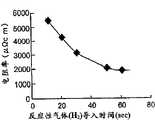
图9是表示本发明第一方面的原料气体导入时间与TaN膜的电阻率的关系的曲线图。Fig. 9 is a graph showing the relationship between the material gas introduction time and the resistivity of the TaN film according to the first aspect of the present invention.
图10是表示本发明第二方面的反应性气体导入时间与已形成的TaN膜的电阻率的关系的曲线图。10 is a graph showing the relationship between the reactive gas introduction time and the resistivity of the formed TaN film according to the second aspect of the present invention.
图11是表示TaN膜的AES分析结果的曲线图。Fig. 11 is a graph showing the results of AES analysis of a TaN film.
图12是该被处理物上形成金属薄膜的状态的示意图。FIG. 12 is a schematic view showing a state where a metal thin film is formed on the object to be processed.
图13是表示本发明第二方面的衬底温度与反射率的关系的曲线图。Fig. 13 is a graph showing the relationship between substrate temperature and reflectance in the second aspect of the present invention.
图14是表示本发明第二方面的压力与反射率的关系的曲线图。Fig. 14 is a graph showing the relationship between pressure and reflectance in the second aspect of the present invention.
图15表示传统技术的成膜装置。Fig. 15 shows a conventional film forming apparatus.
(符号说明)(Symbol Description)
10真空处理装置、11真空室、21催化物、40被处理物。10 vacuum processing device, 11 vacuum chamber, 21 catalyst, 40 object to be processed.
具体实施方式Detailed ways
<真空处理装置><Vacuum treatment device>
图1中符号10表示可在本发明第一、第二方面中利用的真空处理装置,该装置10具有真空室11。该真空室11的底壁上配置了加热板13。该加热板13的周围设有夹子15,将被处理物置放在加热板13上时,通过夹子15保持被处理物。
真空室11内部的加热板13正上方配置有催化物21。该催化物21与电源22相连,驱动电源22,在催化物21中通过直流或交流电而加热该催化物21。这里使用的催化物21是直径为0.5mm、长度为300mm或340mm的钨丝。
真空室11上连接有真空排气系统36,使真空室11成为高真空气氛。在真空室11内成为高真空气氛的状态下,催化物21上通电并使之发热而成为高温。A
真空室11的壁面(顶棚)的催化物21的正上方位置上配置有气体导入口34。真空室11的外部配置了第一~第三气体导入系统31~33,该第一~第三气体导入系统31~33各自连接到气体导入口34。A
本发明的第一方面与第二方面中,充填在第一~第三气体导入系统31~33内的气体互相不同。In the first aspect and the second aspect of the present invention, the gases filled in the first to third
<第一方面相关的装置><Apparatus related to the first aspect>
第一~第三气体导入系统31~33有充填不同种类的反应性气体的气缸。这里,充填在第一~第三气体导入系统31~33的气缸内的反应性气体分别为H2气体、NH3气体、SiH4气体。The first to third
该真空处理装置10中,从气体导入口34可控制流量地导入第一~第三气体导入系统31~33中的任意一个或多个系统中的反应性气体到真空室11内。In the
图2是适用于本发明方法的被处理物40的剖视图。该被处理物40为半导体制造工序中的半导体衬底,其结构为硅衬底41上依次形成第一绝缘膜42、金属布线膜43以及第二绝缘膜44。第二绝缘膜44上形成有沟槽或孔45,沟槽或孔45的底面上露出金属布线膜43。该金属布线膜43为典型的铜薄膜,其按预定平面形状被形成图案。金属布线膜43的一部分与硅衬底41上形成的电气元件电连接。FIG. 2 is a cross-sectional view of an
将真空室11内部成为真空气氛,在维持真空状态下,将上述被处理物40放进真空室11内,并在加热板13上使设有沟槽或孔45的一面朝向催化物21地加以配置。The inside of the
(前处理)(pre-processing)
预先将加热板13通电,放置被处理物40后升温到170~270℃。The
然后,在催化物21上通电加热,使温度上升到预定温度的状态下,从第一~第三气体导入系统31~33导入反应性气体。这里,作为反应性气体,只从第一气体导入系统31导入H2气体。Then, the reaction gas is introduced from the first to third
该导入量(流量)为200sccm,通过控制真空排气速度,使真空室11内的压力保持在0.8~65Pa范围内。The introduction amount (flow rate) is 200 sccm, and the pressure in the
作为催化物21使用的是直径为0.5mm、长度为300mm的钨丝。对催化物21的接通电力设定为直流电压13.0V、14.0A,将催化物21升温到1700℃。A tungsten wire with a diameter of 0.5 mm and a length of 300 mm was used as the
与催化物21相接触的反应性气体生成氢游离基,该氢游离基还原被处理物40的沟槽或孔45的底面上露出的金属布线膜43表面的氧化物,从而使干净的铜薄膜表面露出。The reactive gas in contact with the
这里,催化物21处于高温状态下,导入60秒钟反应性气体(H2气体),从而去除沟槽或孔45的底面的金属布线膜43表面的氧化物。Here, the
如果不同于上述方法,即单独导入NH3气体、SiH4气体,或者导入H2气体、NH3气体和SiH4气体中的两种以上混合气体时,所产生的效果与只导入H2气体时的效果相同,均能去除沟槽或孔45的底面的金属布线膜43表面的氧化物。If it is different from the above method, that is, when introducing NH3 gas, SiH4 gas alone, or introducing two or more mixed gases of H2 gas, NH3 gas and SiH4 gas, the effect produced is the same as when only H2 gas is introduced. The effect is the same, and the oxide on the surface of the
<第二方面相关的装置><A device related to the second aspect>
第一~第三气体导入系统31~33有充填不同种类的处理气体的气缸。这里,充填在第一~第三气体导入系统31~33的气缸内的处理气体分别为H2气体、NH3气体、SiH4气体。The first to third
该真空处理装置10中,从气体导入口34可控制流量地导入第一~第三气体导入系统31~33中的任意一个或多个系统中的处理气体到真空室11内。In the
图2是适用于本发明方法的被处理物40的剖视图。该被处理物40为半导体制造工序中的半导体衬底,在硅衬底41上依次形成第一绝缘膜42、金属薄膜43和第二绝缘膜44。该第二绝缘膜44上形成有沟槽或孔45,沟槽或孔45的底面上露出金属薄膜43。该金属薄膜43为典型的铜薄膜,其按预定平面形状被形成图案。金属薄膜43的一部分与硅衬底41上形成的电气元件相连接。FIG. 2 is a cross-sectional view of an
使真空室11的内部成为真空气氛,并维持真空状态下,将上述的被处理物40放进真空室11内,并在加热板13上使设有沟槽或孔45的一面朝向催化物21地加以配置。Make the inside of the vacuum chamber 11 a vacuum atmosphere, and maintain the vacuum state, put the above-mentioned object to be processed 40 into the
预先将加热板13通电,放置被处理物40后升温到170~270℃。The
然后,在催化物21上通电加热,使温度上升到预定温度的状态下,从第一~第三气体导入系统31~33导入处理气体。这里,作为处理气体,只从第一气体导入系统31导入H2气体。Then, the
该导入量(流量)为200sccm,通过控制真空排气速度,使真空室11内的压力保持在0.8~65Pa范围内。The introduction amount (flow rate) was 200 sccm, and the pressure in the
作为催化物21使用的是直径为0.5mm、长度为300mm的钨丝,从电源22输出11.0V的直流电压时,通电量成为11.0A。这种条件下,催化物21的温度成为1700℃。A tungsten wire with a diameter of 0.5 mm and a length of 300 mm was used as the
与催化物21相接触的处理气体生成氢游离基,该氢游离基还原被处理物40的沟槽或孔45的底面上露出的金属薄膜43表面的氧化物,从而使干净的铜薄膜表面露出。The processing gas in contact with the
这里,催化物21处于高温状态下,导入60秒钟处理气体(H2气体),从而去除沟槽或孔45的底面的金属薄膜43表面的氧化物。Here, the
如果不同于上述方法,即单独导入NH3气体、SiH4气体或H2O气体中的一种,或者导入H2气体、NH3气体、SiH4气体和H2O气体中的两种以上混合气体时,所产生的效果与只导入H2气体时的效果相同,均能去除沟槽或孔45的底面的金属薄膜43表面的氧化物。If it is different from the above method, that is, introduce one of NH3 gas, SiH4 gas or H2 O gas alone, or introduce a mixture of two or more of H2 gas, NH3 gas, SiH4 gas and H2 O gas gas, the effect produced is the same as that of only introducingH2 gas, and the oxides on the surface of the
图1所示的真空处理装置10中,符号35表示金属薄膜的原料气体导入系统,在去除金属薄膜43表面的氧化物后,以维持真空气氛状态,从原料气体导入系统35导入原料气体时,在被处理物40的表面上成长金属薄膜等的导电性薄膜。In the
图3中的符号46表示该金属薄膜,沟槽或孔45的内部被该金属薄膜所覆盖。这里,作为金属薄膜成长钛(Ta)薄膜时,被使用的原料气体可为TIMATA(Ta[NC(CH3)2C2H5][N(CH3)2]3)或PDMAT(TA[N(CH3)2]5)等的有机金属调料(Sauce)。
TIMATA或PDMAT导入加温到80℃的容器内,并将流量控制的Ar气体导入并加以沸腾(bubbling),从而可与Ar气体一起导入到真空室11内。TIMATA or PDMAT is introduced into a container heated to 80° C., and a flow-controlled Ar gas is introduced and bubbling, so that it can be introduced into the
其导入通道,可以不使TIMATA或PDMAT液化地加以配管且预先将腔室加热到80~90℃。The introduction channel may be piped without liquefying TIMATA or PDMAT, and the chamber may be heated to 80-90°C in advance.
上述方法中,铜薄膜的清洗处理与金属薄膜的形成工序是在同一真空室11内进行,且并不将被处理物暴露在空气而维持真空气氛的同时连续进行清洗和金属薄膜的形成,但可以使用各自不同的真空室进行以上工序。这种情况下,需要在本发明方法的清洗工序和金属薄膜形成工序之间,维持被处理物周围的真空气氛。In the above method, the cleaning process of the copper thin film and the forming process of the metal thin film are carried out in the
<第一方面的实施例><Example of the first aspect>
(实施例1)(Example 1)
如图1所示的真空处理装置10中,符号35表示阻障膜的原料气体导入系统,容器37内配置阻障膜的原料38。In the
作为原料38使用有机金属化合物即TIMATA(Ta[NC(CH3)2C2H5][N(CH3)2]3),容器37加热到80℃,导入使TIMATA液化后加以流量控制的载流(carrier)气体,并通过沸腾,作为原料气体生成TIMATA的气体,通过配管39导入到真空室11内。这里,作为载流气体使用100sccm的Ar气体。TIMATA (Ta[NC(CH3 )2 C2 H5 ][N(CH3 )2 ]3 ), which is an organometallic compound, was used as the
配管39及真空室11加热到80~90℃,以为TIMATA在原料气体导入通道中不被液化。The piping 39 and the
增加在加热板13的通电量,经上述<前处理>结束氧化物除去工序后,将被处理物40升温到300~380℃,然后,将原料气体与反应性气体同时导入到真空室内,并将真空室11内的压力维持在2.0Pa。Increase the current flow on the
这里,催化物21的温度维持在1700℃左右,导入的反应性气体被加热的钨丝分解,生成游离基。例如,由NH3气体会分解生成NH游离基与NH2游离基。Here, the temperature of the
这些游离基与作为金属原料气体的TIMATA在加热后的被处理物40上进行化学气相反应(CVD)。如图12所示,在绝缘膜44的表面和沟槽或孔45的侧面或底面露出的金属布线膜43的表面上形成薄膜47。在本实施例中形成的薄膜47为TaxN膜,作为阻障膜具有防止在该薄膜47上形成的铜膜的扩散的功能。These radicals undergo a chemical vapor phase reaction (CVD) with TIMATA, which is a metal source gas, on the
在本实施例中使用的反应性气体是NH3气体,但可以使用H2气体、SiH4气体、NH2NH2气体或H2O气体。这些气体的使用不限于其中任一种,可用两种以上的气体一起使用。The reactive gas used in this embodiment is NH3 gas, but H2 gas, SiH4 gas, NH2 NH2 gas, or H2 O gas may be used. Use of these gases is not limited to any one of them, and two or more gases may be used together.
(测定结果)(The measurement results)
图4是表示以上述条件成膜时和不加热催化物21而在与传统的热CVD法相同的条件下成膜时的TaxN膜的电阻率与被处理物的温度关系的曲线图。4 is a graph showing the relationship between the resistivity of theTax N film and the temperature of the object to be processed when the film is formed under the above conditions and when the
依据本发明方法,可知被处理物的温度到370℃为止,电阻率随着温度的上升而下降。According to the method of the present invention, it can be seen that the temperature of the object to be processed is up to 370°C, and the resistivity decreases as the temperature rises.
相对于此,在传统技术的热CVD法中,即使被处理物的温度提高,TaN膜的电阻率也只降到20000μΩcm左右。On the other hand, in the conventional thermal CVD method, even if the temperature of the object to be processed is increased, the resistivity of the TaN film only drops to about 20000 μΩcm.
接着,图5、图6表示将各被处理物升温到350℃时形成的TaN膜的AES分析的结果,其中,横轴表示蚀刻时间、即表示膜厚方向的深度,纵轴表示构成原子的浓度。图5是按照本发明形成的膜的分析结果,图6是通过不加热催化物的传统技术的热CVD法形成的膜的分析结果。从该结果可以看出,本发明的TaN膜相对传统技术的TaN膜,其含碳量低2.4%。Next, FIG. 5 and FIG. 6 show the results of AES analysis of the TaN film formed when the temperature of each object to be processed was raised to 350°C, wherein the horizontal axis represents the etching time, that is, the depth in the film thickness direction, and the vertical axis represents the concentration of the constituent atoms. concentration. FIG. 5 is an analysis result of a film formed according to the present invention, and FIG. 6 is an analysis result of a film formed by a conventional thermal CVD method without heating a catalyst. It can be seen from the results that the TaN film of the present invention has a carbon content 2.4% lower than that of the conventional TaN film.
图7表示按照本发明制作的O2含量为2.5%的TaN膜与O2含量为5.4%的TaN膜中包含的C成分的原子数比和电阻率的关系。依该结果可以看出,随着C成分减少,电阻率会急剧下降。FIG. 7 shows the relationship between the atomic number ratio and resistivity of the C component contained in a TaN film with an O2 content of 2.5% and a TaN film with an O2 content of 5.4% fabricated according to the present invention. From this result, it can be seen that the resistivity drops sharply as the C component decreases.
发明人认为,本发明的TaN膜的电阻率相对用传统的热CVD法形成的TaN膜偏低的理由在于碳成分的含有率相对低。The inventors believe that the reason why the resistivity of the TaN film of the present invention is lower than that of the TaN film formed by the conventional thermal CVD method is that the content of the carbon component is relatively low.
如上所述,依据本发明,能够形成比传统的热CVD法更加优质的TaN膜。As described above, according to the present invention, it is possible to form a TaN film of higher quality than the conventional thermal CVD method.
(实施例2)(Example 2)
但是,如上述图4的曲线图所示,为了得到2200μΩcm的TaN膜而必须将被处理物加热到375℃。但是目前对Cu布线工序的处理温度要求在300℃以下,因此需要进一步的低温化。However, as shown in the above-mentioned graph of FIG. 4 , in order to obtain a TaN film of 2200 μΩcm, it is necessary to heat the object to be processed to 375° C. However, at present, the processing temperature of the Cu wiring process is required to be below 300°C, so further lowering of the temperature is required.
一边将真空室11排气成为真空,一边将被处理物配置在真空室11内,加热催化物21后,继续排气并加热催化物21,同时交互导入原料气体(TIMATA)和反应性气体(NH3气体或H2气体)。While evacuating the
图8是各气体导入的定时图,其中,符号t1表示原料气体的导入时间、符号t2表示停止导入原料气体后,导入反应性气体前的排气时间、符号t3表示反应性气体的导入时间、符号t4表示停止导入反应性气体后,导入原料气体前的排气时间。Fig. 8 is a timing diagram of the introduction of each gas, wherein symbolt1 represents the introduction time of the raw material gas, symbolt2 represents the exhaust time before introducing the reactive gas after stopping the introduction of the raw material gas, and symbolt3 represents the exhaust time of the reactive gas The introduction time, symbol t4, represents the evacuation time before the introduction of the raw material gas after the introduction of the reactive gas is stopped.
导入原料气体的时间t1期间内不导入反应性气体,导入反应性气体的时间t3期间内不导入原料气体。The reactive gas is not introduced during the timet1 when the raw material gas is introduced, and the raw material gas is not introduced during the timet3 when the reactive gas is introduced.
由于真空室11内部继续进行真空排气系统排气操作,在停止原料气体的导入和反应性气体的导入的状态下,真空室内部的残留气体被排气成为真空。Since the exhaust operation of the vacuum exhaust system is continued inside the
图9表示原料气体的导入时间t1和所得到的TaN膜的关系。FIG. 9 shows the relationship between the introduction timet1 of the source gas and the obtained TaN film.
原料气体的导入时间t1为3~10秒钟,停止导入原料气体到导入反应性气体前的时间t2为5秒,反应性气体的导入时间t3为20秒,停止导入反应性气体到导入原料气体前的时间t4为5秒。The introduction timet1 of the raw material gas is 3 to 10 seconds, the timet2 from the stop of the introduction of the raw material gas to the introduction of the reactive gas is 5 seconds, the introduction timet3 of the reactive gas is 20 seconds, and the time t2 from the stop of the introduction of the reactive gas to the The timet4 before introducing the raw material gas was 5 seconds.
被处理物的温度有280℃、300℃、320℃三种。其他条件与实施例1相同。There are three kinds of temperature for the object to be treated: 280°C, 300°C, and 320°C. Other conditions are identical with
如果将时间t1~t4称为1周期,则经过150周期形成TaN膜。If the time t1 to t4 is referred to as one cycle, the TaN film is formed over 150 cycles.
结果如图9所示。横轴表示原料气体导入时间、纵轴表示电阻率。原料气体导入时间越短,电阻率就越小。认为在被处理物表面吸附的原料气体中,只有表面附近的原子层与游离基进行反应,但由于1周期中的原料气体导入时间越短其1周期中吸附在表面的原子层越薄,与游离基反应的低电阻的TaN膜的比例增大、碳元素的残留量减少,因此认为形成的TaN膜的电阻率下降。The result is shown in Figure 9. The horizontal axis represents the material gas introduction time, and the vertical axis represents the resistivity. The shorter the material gas introduction time, the smaller the resistivity. It is considered that in the raw material gas adsorbed on the surface of the object to be treated, only the atomic layer near the surface reacts with the radicals, but since the introduction time of the raw material gas in one cycle is shorter, the atomic layer adsorbed on the surface in one cycle is thinner. The ratio of the low-resistance TaN film reacted by radicals increases and the residual amount of carbon element decreases, so the resistivity of the formed TaN film is considered to be lowered.
从而,预计在缩短1周期中原料气体的导入时间时,电阻率会进一步下降。Therefore, it is expected that the resistivity will further decrease when the introduction time of the raw material gas in one cycle is shortened.
(实施例3)(Example 3)
图10表示被处理物的温度为300℃、原料气体(TIMATA)的导入时间t1为3秒,排气时间t2、t4为5秒时的、反应性气体(H2气体)的导入时间t3与已形成的TaN膜的电阻率的关系的曲线图。Fig. 10 shows the introduction of reactive gas (H2 gas) when the temperature of the object to be processed is 300°C, the introduction timet1 of the raw material gas (TIMATA) is 3 seconds,and the exhaust timest2 andt4 are 5 seconds Graph of timet3 versus resistivity of the formed TaN film.
Cu布线工艺的上限温度为300℃,但从图10的结果来看,即使被处理物的加热温度为300℃,其电阻率也是2000μΩcm。The upper limit temperature of the Cu wiring process is 300°C, but from the results in Figure 10, even if the object to be processed is heated at 300°C, its resistivity is 2000μΩcm.
另外,图11表示该TaN膜的AES分析的结果。可以看出,影响薄膜质量的碳成分含有率明显低于传统的CVD法,大约1.5%。该值也低于图5情况下的值。In addition, FIG. 11 shows the results of AES analysis of this TaN film. It can be seen that the content of carbon components affecting the quality of the film is significantly lower than that of the traditional CVD method, about 1.5%. This value is also lower than that in the case of Fig. 5 .
通过上述方法,本发明方法可满足Cu布线工艺的要求,即Through the above method, the method of the present invention can meet the requirements of the Cu wiring process, namely
(1)300℃以下的衬底温度(1) Substrate temperature below 300°C
(2)无碳成分的优质膜(2) High-quality film without carbon components
(3)良好的STEP COVERAGE(3) Good STEP COVERAGE
还有,以上就TaN膜的形成方法进行了说明,但本发明并不仅限于TaN膜的形成方法,可以广泛应用于真空气氛中导入原料气体和反应性气体,并使加热的催化物与反应性气体相接触而生成游离基,该游离基与原料气体进行化学反应,在被处理物表面上形成薄膜的工艺中。In addition, the formation method of the TaN film has been described above, but the present invention is not limited to the formation method of the TaN film, and can be widely used in introducing raw material gas and reactive gas in a vacuum atmosphere, and making the heated catalyst and reactive gas In the process of forming a thin film on the surface of the object to be processed, the gas is contacted to generate free radicals, and the free radicals chemically react with the raw material gas.
<第二方面的实施例><Example of the second aspect>
表示铜薄膜表面的清洁度的指标可用反射率。反射率是指某一波长的光束照射在衬底表面时,相对于入射时光强的反射时光强的比例,反射率越大,说明该衬底越接近镜面。Reflectance can be used as an index representing the cleanliness of the copper thin film surface. The reflectivity refers to the ratio of the reflected light intensity to the incident light intensity when a beam of a certain wavelength is irradiated on the surface of the substrate. The greater the reflectivity, the closer the substrate is to the mirror surface.
设硅晶片的镜面反射率以100%为标准时,无氧化物的干净铜薄膜表面在波长436nm的情况下,其反射率为120%左右。Assuming that the specular reflectance of the silicon wafer is 100% as the standard, the reflectance of the oxide-free clean copper film surface is about 120% at a wavelength of 436nm.
为了测定本发明的效果,用铜薄膜表面全部露出的衬底替换被处理物40,然后,以反射率的变化作为铜薄膜表面的氧化物去除状态加以求得。In order to measure the effect of the present invention, the
通常的半导体装置的衬底中,该铜薄膜表面几乎没有被氧化,其反射率大致120%左右,但适用本发明方法的衬底的铜薄膜的反射率为15~20%。In a typical substrate of a semiconductor device, the surface of the copper thin film is hardly oxidized, and its reflectance is about 120%. However, the reflectance of the copper thin film of the substrate to which the method of the present invention is applied is 15 to 20%.
(实施例1)(Example 1)
处理气体为H2气体,流量为200SCCM,腔室压力65Pa,处理气体导入时间60秒钟。衬底温度分别为170℃、230℃、270℃三种。The processing gas is H2 gas, the flow rate is 200SCCM, the chamber pressure is 65Pa, and the processing gas introduction time is 60 seconds. The substrate temperature is 170°C, 230°C, and 270°C respectively.
(比较例1)(comparative example 1)
为了作比较,在催化物21上不通电的情况下,衬底加热到分别为170℃、230℃、270℃、350℃,然后导入处理气体,将铜薄膜表面的氧化物还原。其他条件与实施例1相同。For comparison, when the
(测定结果1)(measurement result 1)
图13表示反射率测定结果。横轴表示衬底温度、纵轴表示反射率。Fig. 13 shows the reflectance measurement results. The horizontal axis represents the substrate temperature, and the vertical axis represents the reflectance.
如图13所示,利用本发明方法时,衬底温度为170℃时反射率可达到125%,与之相比,比较例中衬底温度即使成为350℃其反射率也达不到120%。As shown in Figure 13, when using the method of the present invention, the reflectance can reach 125% when the substrate temperature is 170°C. In contrast, the reflectance cannot reach 120% even if the substrate temperature is 350°C in the comparative example. .
可以看出,依据本发明的方法,在低温也可清除铜薄膜表面的氧化物,使干净的铜薄膜表面露出,但在比较例中,铜薄膜表面并没有得到清洁。It can be seen that according to the method of the present invention, the oxide on the surface of the copper film can also be removed at low temperature, so that the clean surface of the copper film is exposed, but in the comparative example, the surface of the copper film is not cleaned.
实际上,半导体制造工序中,只用H2气体和加热衬底的方式的清洗铜薄膜的清洗工序中,通常把被处理物的温度升高到300℃左右,但是依据本发明方法可实现200℃左右的低温化。In fact, in the semiconductor manufacturing process, the temperature of the object to be processed is usually raised to about 300°C in the cleaning process of cleaning the copper film by using onlyH2 gas and heating the substrate, but according to the method of the present invention, 200°C can be realized. ℃ low temperature.
相反,用本发明方法时,当被处理物的温度提高到300℃左右时,可得到比低温时更加干净的铜薄膜表面。On the contrary, when the method of the present invention is used, when the temperature of the object to be processed is increased to about 300°C, a cleaner copper film surface can be obtained than at a low temperature.
(实施例2)(Example 2)
接着,将反射率与实施例1用的衬底相同的衬底放置在真空室11内,变化压力并处理衬底,测定反射率。Next, a substrate having the same reflectance as that used in Example 1 was placed in the
衬底温度为230℃,H2气体流量为200SCCM,真空室内的压力为0.8Pa、10Pa、65Pa,处理时间为60秒。The substrate temperature is 230°C, the H2 gas flow rate is 200SCCM, the pressure in the vacuum chamber is 0.8Pa, 10Pa, 65Pa, and the processing time is 60 seconds.
(测定结果2)(measurement result 2)
测定结果如图14所示。该图中横轴表示处理压力、纵轴表示反射率。The measurement results are shown in FIG. 14 . In the figure, the horizontal axis represents the processing pressure, and the vertical axis represents the reflectance.
从该结果可以看出,铜薄膜表面的清洁处理对压力的依赖性很小。From this result, it can be seen that the cleaning treatment of the copper film surface has little dependence on pressure.
利用等离子进行表面处理时,若处理压力减小,则等离子密度也随之降低,因此,其效率也大幅下降。例如压力减少2成,等离子密度也下降2成。When using plasma for surface treatment, if the treatment pressure is reduced, the plasma density will also be reduced, and therefore, its efficiency will also be greatly reduced. For example, if the pressure is reduced by 20%, the plasma density will also be reduced by 20%.
与之相比,本发明中,如图14所示,即使压力变化2成,其表面清洁的效率也没有变化,其理由认为是游离基的密度比等离子多10~100倍。In contrast, in the present invention, as shown in FIG. 14 , even if the pressure changes by 20%, the efficiency of surface cleaning does not change. The reason for this is that the density of free radicals is 10 to 100 times higher than that of plasma.
以上,主要是针对铜薄膜表面的清洗进行了说明,但本发明的清洗对象并不限于铜薄膜,还可以广泛用于TiN、Al或Si结晶等的导电性物质的表面、或者其薄膜表面的清洗。特别是,适用于设在绝缘膜上的细孔或沟槽的底面下方露出导电性物质的或那些薄膜表面的清洗工序中。Above, the cleaning of the copper thin film surface has been mainly explained, but the cleaning object of the present invention is not limited to the copper thin film, and can also be widely used for cleaning the surface of conductive substances such as TiN, Al or Si crystals, or the surface of its thin film. cleaning. In particular, it is suitable for cleaning the surface of thin holes or grooves provided in insulating films where conductive substances are exposed below the bottom surfaces.
Claims (2)
Translated fromChineseApplications Claiming Priority (6)
| Application Number | Priority Date | Filing Date | Title |
|---|---|---|---|
| JP2003390391 | 2003-11-20 | ||
| JP2003-390391 | 2003-11-20 | ||
| JP2003390391AJP2005158761A (en) | 2003-11-20 | 2003-11-20 | Thin film manufacturing method, semiconductor device and manufacturing method thereof |
| JP2003401195 | 2003-12-01 | ||
| JP2003401195AJP2005166783A (en) | 2003-12-01 | 2003-12-01 | Method for cleaning surface of semiconductor substrate |
| JP2003-401195 | 2003-12-01 |
Related Parent Applications (1)
| Application Number | Title | Priority Date | Filing Date |
|---|---|---|---|
| CN2004100957620ADivisionCN1638052B (en) | 2003-11-20 | 2004-11-19 | Method for producing thin film |
Publications (2)
| Publication Number | Publication Date |
|---|---|
| CN101330044Atrue CN101330044A (en) | 2008-12-24 |
| CN101330044B CN101330044B (en) | 2011-01-12 |
Family
ID=34717783
Family Applications (1)
| Application Number | Title | Priority Date | Filing Date |
|---|---|---|---|
| CN200810125094XAExpired - LifetimeCN101330044B (en) | 2003-11-20 | 2004-11-19 | film manufacturing method |
Country Status (2)
| Country | Link |
|---|---|
| JP (1) | JP2005158761A (en) |
| CN (1) | CN101330044B (en) |
Cited By (4)
| Publication number | Priority date | Publication date | Assignee | Title |
|---|---|---|---|---|
| CN105742157A (en)* | 2014-12-30 | 2016-07-06 | Asm Ip控股有限公司 | Germanium Oxide Pre-Clean Module And Process |
| CN109804110A (en)* | 2016-10-04 | 2019-05-24 | 碳能力有限责任公司 | Apparatus and method for laying carbon layers |
| US10373850B2 (en) | 2015-03-11 | 2019-08-06 | Asm Ip Holding B.V. | Pre-clean chamber and process with substrate tray for changing substrate temperature |
| CN111107949A (en)* | 2017-12-18 | 2020-05-05 | 积水化学工业株式会社 | Surface treatment method and apparatus |
Families Citing this family (3)
| Publication number | Priority date | Publication date | Assignee | Title |
|---|---|---|---|---|
| EP2039799A4 (en)* | 2006-04-18 | 2015-09-30 | Ulvac Inc | Film forming apparatus and barrier film manufacturing method |
| JP6041464B2 (en)* | 2011-03-03 | 2016-12-07 | 大陽日酸株式会社 | Metal thin film forming method and metal thin film forming apparatus |
| US11410881B2 (en)* | 2020-06-28 | 2022-08-09 | Applied Materials, Inc. | Impurity removal in doped ALD tantalum nitride |
Family Cites Families (3)
| Publication number | Priority date | Publication date | Assignee | Title |
|---|---|---|---|---|
| JP3436776B2 (en)* | 1993-08-09 | 2003-08-18 | 忠弘 大見 | Wafer cleaning apparatus and cleaning method |
| US6040010A (en)* | 1996-09-10 | 2000-03-21 | Micron Technology, Inc. | Catalytic breakdown of reactant gases in chemical vapor deposition |
| CN1313412A (en)* | 2000-03-10 | 2001-09-19 | 广镓光电股份有限公司 | Method, product and equipment for forming group III nitride epitaxial layer on single crystal substrate |
- 2003
- 2003-11-20JPJP2003390391Apatent/JP2005158761A/enactivePending
- 2004
- 2004-11-19CNCN200810125094XApatent/CN101330044B/ennot_activeExpired - Lifetime
Cited By (8)
| Publication number | Priority date | Publication date | Assignee | Title |
|---|---|---|---|---|
| CN105742157A (en)* | 2014-12-30 | 2016-07-06 | Asm Ip控股有限公司 | Germanium Oxide Pre-Clean Module And Process |
| CN105742157B (en)* | 2014-12-30 | 2019-08-27 | Asm Ip控股有限公司 | Germanium Oxide Preclean Module and Method |
| US10373850B2 (en) | 2015-03-11 | 2019-08-06 | Asm Ip Holding B.V. | Pre-clean chamber and process with substrate tray for changing substrate temperature |
| US11264255B2 (en) | 2015-03-11 | 2022-03-01 | Asm Ip Holding B.V. | Pre-clean chamber and process with substrate tray for changing substrate temperature |
| CN109804110A (en)* | 2016-10-04 | 2019-05-24 | 碳能力有限责任公司 | Apparatus and method for laying carbon layers |
| CN109804110B (en)* | 2016-10-04 | 2021-03-30 | 碳能力有限责任公司 | Apparatus and method for laying carbon layers |
| US11746415B2 (en) | 2016-10-04 | 2023-09-05 | Carboncompetence Gmbh | Method for applying a carbon layer to a substrate comprising introducing a process gas into a deposition chamber via a gas inlet and gas activation element |
| CN111107949A (en)* | 2017-12-18 | 2020-05-05 | 积水化学工业株式会社 | Surface treatment method and apparatus |
Also Published As
| Publication number | Publication date |
|---|---|
| CN101330044B (en) | 2011-01-12 |
| JP2005158761A (en) | 2005-06-16 |
Similar Documents
| Publication | Publication Date | Title |
|---|---|---|
| TWI868200B (en) | Gap fill deposition process | |
| US6734102B2 (en) | Plasma treatment for copper oxide reduction | |
| TWI404816B (en) | Method and apparatus for photo-excitation of chemicals for atomic layer deposition of dielectric film | |
| US8183150B2 (en) | Semiconductor device having silicon carbide and conductive pathway interface | |
| US11791181B2 (en) | Methods for the treatment of workpieces | |
| KR101764163B1 (en) | A method for capping a copper surface on a substrate | |
| TWI394858B (en) | Method of depositing tungsten film with reduced resistivity and improved surface morphology | |
| KR102503141B1 (en) | Pulsed nitride encapsulation | |
| JP4974676B2 (en) | Formation method of barrier film | |
| CN110622283B (en) | Method for reducing or eliminating defects in tungsten films | |
| TW201718923A (en) | Selective deposition of aluminum and nitrogen containing material | |
| JP2005347472A (en) | Substrate processing method and manufacturing method of semiconductor device | |
| KR101739613B1 (en) | Method for forming copper wiring | |
| EP3216048A1 (en) | Methods for thermally forming a selective cobalt layer | |
| US8216642B2 (en) | Method of manufacturing film | |
| KR19990068219A (en) | Chemical vapor phase growing method of a metal nitride film and a method of manufacturing an electronic device using the same | |
| CN101330044B (en) | film manufacturing method | |
| US20210062330A1 (en) | Selective cobalt deposition on copper surfaces | |
| US20230407465A1 (en) | METHOD OF FORMING SiOCN LAYER | |
| TWI609095B (en) | Methods for manganese nitride integration | |
| KR102597990B1 (en) | Method for selective deposition of aluminum and nitrogen containing material | |
| JP2005166783A (en) | Method for cleaning surface of semiconductor substrate | |
| KR20240113592A (en) | Tungsten fluoride immersion and treatment for tungsten oxide removal |
Legal Events
| Date | Code | Title | Description |
|---|---|---|---|
| C06 | Publication | ||
| PB01 | Publication | ||
| C10 | Entry into substantive examination | ||
| SE01 | Entry into force of request for substantive examination | ||
| C14 | Grant of patent or utility model | ||
| GR01 | Patent grant | ||
| CX01 | Expiry of patent term | ||
| CX01 | Expiry of patent term | Granted publication date:20110112 |