CN101327575A - grinding head - Google Patents
grinding headDownload PDFInfo
- Publication number
- CN101327575A CN101327575ACNA200710112605XACN200710112605ACN101327575ACN 101327575 ACN101327575 ACN 101327575ACN A200710112605X ACNA200710112605X ACN A200710112605XACN 200710112605 ACN200710112605 ACN 200710112605ACN 101327575 ACN101327575 ACN 101327575A
- Authority
- CN
- China
- Prior art keywords
- grinding head
- grinding
- inner ring
- outer ring
- ring part
- Prior art date
- Legal status (The legal status is an assumption and is not a legal conclusion. Google has not performed a legal analysis and makes no representation as to the accuracy of the status listed.)
- Pending
Links
- 239000000126substanceSubstances0.000claimsabstractdescription20
- 238000000034methodMethods0.000claimsabstractdescription12
- 238000005498polishingMethods0.000abstractdescription36
- 238000007517polishing processMethods0.000description11
- 238000010586diagramMethods0.000description8
- 239000000463materialSubstances0.000description7
- 238000009826distributionMethods0.000description5
- 238000004519manufacturing processMethods0.000description5
- 230000000694effectsEffects0.000description4
- 238000005516engineering processMethods0.000description3
- 230000000052comparative effectEffects0.000description2
- 238000005520cutting processMethods0.000description2
- 238000007667floatingMethods0.000description2
- 230000004048modificationEffects0.000description2
- 238000012986modificationMethods0.000description2
- 239000002002slurrySubstances0.000description2
- 239000000654additiveSubstances0.000description1
- 230000015572biosynthetic processEffects0.000description1
- 239000003153chemical reaction reagentSubstances0.000description1
- 238000000465mouldingMethods0.000description1
- 238000003825pressingMethods0.000description1
- 239000004065semiconductorSubstances0.000description1
- 239000007787solidSubstances0.000description1
Images


Landscapes
- Mechanical Treatment Of Semiconductor (AREA)
- Finish Polishing, Edge Sharpening, And Grinding By Specific Grinding Devices (AREA)
Abstract
Description
Translated fromChinese技术领域technical field
本发明有关于一种集成电路装置,特别是有关于一种研磨头。The present invention relates to an integrated circuit device, in particular to a grinding head.
背景技术Background technique
在半导体工艺技术中,化学机械研磨的原理是利用类似磨刀的机械式原理,配合适当的化学助剂(reagent),将研磨垫(polishing pad)上的晶片表面高低起伏不一的轮廓加以磨平。一般来说,化学机械研磨装置大多使用研磨头抓住晶片,然后把晶片的正面压在供有研浆(slurry)的研磨垫上进行研磨。在化学机械研磨的过程中,由于机械结构上的限制,而使研磨头上的压力无法全面一致,造成部分区域的研磨率会过高或过低。In semiconductor process technology, the principle of chemical mechanical polishing is to use the mechanical principle similar to sharpening a knife, with appropriate chemical additives (reagent), to grind the uneven contour of the wafer surface on the polishing pad. flat. Generally speaking, most chemical mechanical polishing devices use a polishing head to grasp the wafer, and then press the front side of the wafer on a polishing pad provided with slurry for polishing. During the chemical mechanical polishing process, due to the limitation of the mechanical structure, the pressure on the polishing head cannot be fully consistent, resulting in the polishing rate of some areas being too high or too low.
公知技术利用施以不同的背压于研磨头,也就是使用类似气囊(air bag)以浮动式背压的方式来调整压力,改善研磨率不一致的问题。但是,以浮动式背压的方式加压于研磨头容易因为气压的控制不稳定,而导致加压效果不佳。此外,在公知技术中,也有通过于表面平整的研磨头上覆盖载膜(carrierfilm),并在研磨率较低的位置,例如是研磨头的边缘,于载膜上加垫一块带(tape)来加大压力。然而,加垫于研磨头上的带的厚度必须非常薄,通常为30μm,使得在制造的过程中,带的品质不易控制。因此,上述两种公知技术会因为气压控制不稳定或是由于耗材制造品质的差异,使研磨率均匀性改善的效果有限,无法达到预期的目的。The known technology utilizes applying different back pressures to the grinding head, that is, using a floating back pressure similar to an air bag to adjust the pressure, so as to improve the problem of inconsistency in the grinding rate. However, applying pressure to the grinding head in the form of floating back pressure is likely to result in poor pressurization effect due to unstable control of the air pressure. In addition, in the known technology, there is also a carrier film (carrier film) covered on the grinding head with a flat surface, and a piece of tape (tape) is placed on the carrier film at a position where the grinding rate is low, such as the edge of the grinding head. Come up the pressure. However, the thickness of the belt on the grinding head must be very thin, usually 30 μm, making it difficult to control the quality of the belt during the manufacturing process. Therefore, the above two known techniques have limited effect on improving the uniformity of the grinding rate due to unstable air pressure control or differences in the manufacturing quality of the consumables, and cannot achieve the desired purpose.
发明内容Contents of the invention
本发明所要解决的技术问题提供一种研磨头,不需使用耗材就能提升研磨头边缘的研磨率,以改善研磨率的均匀性。The technical problem to be solved by the present invention is to provide a grinding head, which can increase the grinding rate of the edge of the grinding head without using consumables, so as to improve the uniformity of the grinding rate.
本发明提出一种研磨头,适用于化学机械研磨工艺(chemicalmechanical polishing,CMP)。研磨头包括内圈部与外圈部。外圈部为环状结构,且连接于内圈部。内圈部与外圈部为一体成型的结构。此外,外圈部的表面与内圈部的表面具有段差,使得外圈部的表面高于内圈部的表面。The invention provides a polishing head suitable for chemical mechanical polishing (CMP). The grinding head includes an inner ring part and an outer ring part. The outer ring part is a ring structure and is connected to the inner ring part. The inner ring part and the outer ring part are integrally formed. In addition, the surface of the outer ring portion has a level difference from the surface of the inner ring portion such that the surface of the outer ring portion is higher than the surface of the inner ring portion.
在本发明的一实施例中,上述的段差介于5μm至35μm之间。In an embodiment of the present invention, the aforementioned step difference is between 5 μm and 35 μm.
在本发明的一实施例中,上述的段差为10μm。In an embodiment of the present invention, the aforementioned step difference is 10 μm.
在本发明的一实施例中,上述的内圈部为圆,而外圈部为圆形环。In an embodiment of the present invention, the above-mentioned inner ring part is a circle, and the outer ring part is a circular ring.
在本发明的一实施例中,上述的圆的半径与圆形环的宽度的比介于2∶1至5∶1之间。In an embodiment of the present invention, the ratio of the radius of the circle to the width of the circular ring is between 2:1 and 5:1.
在本发明的一实施例中,上述的圆的半径与圆形环的宽度的比为3∶1。In an embodiment of the present invention, the ratio of the radius of the above-mentioned circle to the width of the circular ring is 3:1.
在本发明的一实施例中,上述的外圈部邻接于内圈部的外缘,且内圈部与外圈部的接面为垂直接面。In an embodiment of the present invention, the above-mentioned outer ring portion is adjacent to the outer edge of the inner ring portion, and a joint surface between the inner ring portion and the outer ring portion is a vertical joint surface.
在本发明的一实施例中,于内圈部与外圈部之间更包括连接环,使内圈部与外圈部相连接。In an embodiment of the present invention, a connecting ring is further included between the inner ring part and the outer ring part to connect the inner ring part and the outer ring part.
在本发明的一实施例中,上述的连接环的表面为斜面。In an embodiment of the present invention, the surface of the above-mentioned connecting ring is a slope.
根据上述方案,本发明相对于现有技术的效果是显著的:According to above-mentioned scheme, the effect of the present invention relative to prior art is remarkable:
本发明的研磨头利用其表面轮廓形成有段差,来调整边缘区域研磨率较低的现象。由于研磨头的外圈部的表面高于内圈部的表面,使得原本研磨率较低的边缘区域的研磨率能够获得提升,以改善研磨率的均匀性。The grinding head of the present invention utilizes the level difference formed in its surface profile to adjust the phenomenon of lower grinding rate in the edge area. Since the surface of the outer ring portion of the grinding head is higher than the surface of the inner ring portion, the grinding rate of the edge region where the grinding rate is originally low can be increased to improve the uniformity of the grinding rate.
此外,本发明的研磨头不需额外使用耗材,如载膜或带,因此可以避免研磨率受到耗材制造品质不一的影响。并可以通过减少耗材的使用,降低研磨头的制作成本。In addition, the grinding head of the present invention does not need to use additional consumables, such as carrier film or belt, so the grinding rate can be avoided from being affected by the manufacturing quality of consumables. And can reduce the production cost of the grinding head by reducing the use of consumables.
再者,利用本发明具有凹凸构形的研磨头来进行晶片的研磨,当施以相同背压于此研磨头时,会在研磨头的外圈部形成较大的压力。因此,能够调整整体的研磨率,而使晶片表面的均匀度可以提升。Furthermore, when using the grinding head with concave-convex configuration of the present invention to grind the wafer, when the same back pressure is applied to the grinding head, a larger pressure will be formed on the outer ring of the grinding head. Therefore, the overall grinding rate can be adjusted, so that the uniformity of the wafer surface can be improved.
附图说明Description of drawings
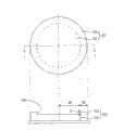
图1A为依照本发明一实施例所绘示的研磨头的俯视图及沿I-I’线段剖面图的投影关系对照示意图。Fig. 1A is a schematic diagram showing a comparison between a top view of a grinding head and a cross-sectional view along line I-I' according to an embodiment of the present invention.
图1B为依照本发明另一实施例所绘示的研磨头的俯视图及沿I-I’线段剖面图的投影关系对照示意图。Fig. 1B is a schematic diagram showing a top view of a grinding head according to another embodiment of the present invention and a cross-sectional view along the I-I' line segment.
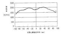
图2为以本发明的研磨头进行化学机械研磨工艺的移除率分布图。FIG. 2 is a distribution diagram of the removal rate of the chemical mechanical polishing process using the polishing head of the present invention.
图3为以公知的覆盖载膜的研磨头进行化学机械研磨工艺的移除率分布图。FIG. 3 is a distribution diagram of the removal rate of a chemical mechanical polishing process using a known polishing head covered with a carrier film.
主要元件符号说明Description of main component symbols
100、200……研磨头 102……内圈部100, 200...Grinding
104…………外圈部 106……连接环104………
106a………表面 108……接面106a……
D……………段差 W1……半径D…………Segment difference W1……Radius
W2……………宽度W2……………Width
具体实施方式Detailed ways
为让本发明的上述特征和优点能更明显易懂,下文特举较佳实施例,并配合所附图式,作详细说明如下。In order to make the above-mentioned features and advantages of the present invention more comprehensible, preferred embodiments will be described in detail below together with the accompanying drawings.
图1A为依照本发明一实施例所绘示的研磨头的俯视图及沿I-I’线段剖面图的投影关系对照示意图。Fig. 1A is a schematic diagram showing a comparison between a top view of a grinding head and a cross-sectional view along line I-I' according to an embodiment of the present invention.
请参照图1A,适用于化学机械研磨工艺的研磨头100例如是一个圆形的结构。研磨头100包括内圈部102以及外圈部104。Referring to FIG. 1A , the
在本实施例中,内圈部102为实心圆形结构,而外圈部104为圆形环状结构。外圈部104环绕于内圈部102的周围,且外圈部104的内缘与内圈部102的外缘相邻接,使二者之间的接面108为垂直接面。内圈部102与外圈部104为一体成型的结构。也就是说,从俯视的角度来看研磨头100,内圈部102与环状的外圈部104例如是共同构成一个同心圆的结构。In this embodiment, the
请参照图1A,在研磨头100的半径截面上,内圈部102的半径W1与外圈部104所占的宽度W2的比例如是介于2∶1至5∶1之间。另一方面,外圈部104的厚度例如是大于内圈部102的厚度,且外圈部104的表面会高于内圈部102的表面,而二者之间的段差D例如是介于5μm至35μm之间。在一实施例中,研磨头100的半径为100mm,内圈部102的半径W1为75mm,外圈部104环状结构的宽度W2则为25mm;而外圈部104表面与内圈部102表面之间的段差D为10μm。Referring to FIG. 1A , on the radius section of the
图1B为依照本发明另一实施例所绘示的研磨头的俯视图及沿I-I’线段剖面图的投影关系对照示意图。于图1B中,与图1A相同的构件则使用相同的标号并省略其说明。Fig. 1B is a schematic diagram showing a top view of a grinding head according to another embodiment of the present invention and a cross-sectional view along the I-I' line segment. In FIG. 1B , the same components as those in FIG. 1A use the same reference numerals and their descriptions are omitted.
请参照图1B,本发明还提出另一种适用于化学机械研磨工艺的研磨头200。组成研磨头200的基本构件与组成研磨头100的基本构件大致相同,其中主要的差异在于:在研磨头200中,于内圈部102与外圈部104之间更包括连接环106,连接内圈部102与外圈部104之间。连接环106为圆形环状结构,且其内缘与内圈部102邻接,其外缘则与外圈部104邻接。连接环106的表面106a例如是斜面,可以将内圈部102的表面与外圈部104的表面连接起来。值得一提的是,连接环106的数量以及表面构造并不局限于图1B所绘示,只要能够使内圈部102与外圈部104相连接并构成一体成形的结构即可,本发明于此不作特别的限定。Please refer to FIG. 1B , the present invention also proposes another polishing
请同时参照图1A与图1B,换言之,研磨头100与研磨头200具有凹凸构形,上述的内圈部102即为凹部,外圈部104为凸部。当然,在其它实施例中,研磨头100与研磨头200的凹部与凸部的配置并不局限于上述的内圈部102与外圈部104,于此领域具有通常知识者可视其需求进行调整。Please refer to FIG. 1A and FIG. 1B at the same time. In other words, the grinding
承上述,内圈部102与外圈部104的结构为一体成型的构造。因此,研磨头100与研磨头200的形成方法是在具有平整表面的刚体材料(未绘示)上,例如是平面研磨头本体,保留研磨率表现较低的边缘位置,在研磨率较高的内圈位置移除部份刚体材料作为内圈部102。移除刚体材料的方法例如是通过切削或是研磨的方式向下切削研磨,使刚体材料上形成具有段差D的内圈部102与外圈部104。而段差D则是利用控制向下切削或研磨的深度来进行调整。当然,内圈部102的半径W1以及段差D可以经由使用研磨头100与研磨头200进行后续的化学机械研磨工艺,所研磨出来的材料层表面轮廓进行修正,以取得最佳化的条件。此外,移除部份刚体材料的位置并不局限于本实施例中所绘示的内圈部102的形成位置,移除部份刚体材料的区域可以为任何研磨率较高而需调整的区域,于此领域具有通常知识者当可视其需求进行调整。Based on the above, the structures of the
特别说明的是,在研磨头100与研磨头200中,具有较高表面的外圈部104是配置于公知平面研磨头中研磨率较低的区域。而使用上述的研磨头100或研磨头200进行化学机械研磨工艺,是先以研磨头100或研磨头200将晶片(未绘示)固定于研磨垫(未绘示)上,其中研磨垫上例如是布满研浆。之后,施以固定背压于研磨头100或研磨头200,再利用研磨垫与晶片的相对移动进行研磨步骤。由于研磨头100与研磨头200具有凹凸构形,即使在施加固定背压的情况下,还是可以通过研磨头100与研磨头200表面轮廓的差异来提供晶片不同的压力。进一步而言,构成凸部的外圈部104会提供较大压力于晶片。因此,在进行研磨步骤时,可以使研磨头100与研磨头200边缘的研磨率获得提升,而改善研磨均匀性。In particular, in the grinding
为证实本发明的研磨头确有其功效,以下特举一个实验例来说明本发明的研磨头应用于化学机械研磨工艺时所达到的效果。In order to prove that the grinding head of the present invention is effective, an experimental example is given below to illustrate the effect achieved when the grinding head of the present invention is applied to a chemical mechanical polishing process.
实验例Experimental example
图2是以本发明的研磨头(如图1A所示的研磨头100)进行化学机械研磨工艺的移除率分布图。FIG. 2 is a distribution diagram of the removal rate of the chemical mechanical polishing process performed by the polishing head of the present invention (the polishing
请参照图2,当使用本发明的研磨头进行化学机械研磨工艺时,是将晶片固定于本发明的研磨头上,再施加固定的背压于研磨头,使晶片压至研磨垫上以进行研磨步骤。从图2的结果中显示,远离圆心的边缘部份的移除率确实可以有效地提升,且整体研磨率的均匀性也获得改善(研磨均匀度为500A/min)。再者,图2中分别绘示的四次数据分布十分一致,显示本发明的研磨头还可以使研磨率有持续稳定的表现。Please refer to Fig. 2, when using the grinding head of the present invention to carry out chemical mechanical polishing process, be that wafer is fixed on the grinding head of the present invention, apply fixed back pressure to grinding head again, make wafer be pressed on the grinding pad to grind step. The results in Figure 2 show that the removal rate of the edge part away from the center of the circle can be effectively improved, and the uniformity of the overall grinding rate is also improved (the grinding uniformity is 500A/min). Furthermore, the four data distributions shown in FIG. 2 are very consistent, which shows that the grinding head of the present invention can also make the grinding rate have a continuous and stable performance.
比较例comparative example
图3是以公知的覆盖载膜的研磨头进行化学机械研磨工艺的移除率分布图。FIG. 3 is a distribution diagram of the removal rate of a chemical mechanical polishing process performed by a known polishing head covered with a carrier film.
比较例与实验例进行化学机械研磨的方法相似,唯一的差别仅在所使用的研磨头不同。请参照图3,在使用仅覆盖载膜的研磨头进行化学机械研磨时,表面为平面的研磨头会造成部分区域的移除率过高或过低,尤其是远离圆心的边缘部份会发生移除率明显降低的问题,而导致均匀性不佳。The chemical mechanical polishing method of the comparative example is similar to that of the experimental example, and the only difference is the used polishing head. Please refer to Figure 3. When using a polishing head that only covers the carrier film for chemical mechanical polishing, the polishing head with a flat surface will cause the removal rate to be too high or too low in some areas, especially at the edge far away from the center of the circle. The removal rate is significantly reduced, resulting in poor uniformity.
由以上实际测试的结果显示:本发明的研磨头不仅可以提升边缘的研磨率,还可以改善研磨率的均匀性并使研磨率稳定表现。The above actual test results show that the grinding head of the present invention can not only increase the grinding rate of the edge, but also improve the uniformity of the grinding rate and stabilize the grinding rate.
综上所述,本发明于研磨头的内圈部形成凹部,使位于研磨头外圈部作为凸部,再施予研磨头固定背压进行化学机械研磨工艺,可以使原本研磨率较低的边缘通过研磨头的凹凸构形造成压力的改变,而使外圈部研磨率增加,因而可以获得较佳的均匀性。In summary, the present invention forms a concave portion on the inner ring of the grinding head, makes the outer ring of the grinding head a convex portion, and then applies a fixed back pressure to the grinding head to perform a chemical mechanical grinding process, which can make the original grinding rate lower The edge changes the pressure through the concave-convex configuration of the grinding head, which increases the grinding rate of the outer ring, so that better uniformity can be obtained.
另一方面,由于本发明的研磨头采用固定式的刚体结构,而不需额外使用载膜或带等耗材,可以避免耗材的制造品质造成研磨率不稳定。此外,此种一体成型的结构在于工艺参数的最佳化及维护上都较为容易,并能获得较大的工艺裕度(process window)。On the other hand, since the grinding head of the present invention adopts a fixed rigid body structure, it does not need additional consumables such as carrier film or belt, which can avoid the unstable grinding rate caused by the manufacturing quality of consumables. In addition, the integral molding structure is easier to optimize and maintain process parameters, and can obtain a larger process window.
再者,本发明通过改变研磨头表面轮廓的简单手段,即可调整部分区域研磨率,达成较佳均匀性的目的,且不需额外使用耗材,可有助于节省工艺成本。Furthermore, the present invention can adjust the grinding rate in some areas by simply changing the surface profile of the grinding head to achieve better uniformity without using additional consumables, which can help save process costs.
虽然本发明已以较佳实施例揭露如上,然而其并非用以限定本发明,任何所属技术领域中具有通常知识者,在不脱离本发明的精神和范围内,当可作些许的更动与润饰,因此本发明的保护范围当视权利要求书所界定的范围为准。Although the present invention has been disclosed above with a preferred embodiment, it is not intended to limit the present invention. Anyone with ordinary knowledge in the technical field may make some modifications and changes without departing from the spirit and scope of the present invention. Modification, therefore, the protection scope of the present invention should be determined by the scope defined in the claims.
Claims (9)
Translated fromChinesePriority Applications (1)
| Application Number | Priority Date | Filing Date | Title |
|---|---|---|---|
| CNA200710112605XACN101327575A (en) | 2007-06-22 | 2007-06-22 | grinding head |
Applications Claiming Priority (1)
| Application Number | Priority Date | Filing Date | Title |
|---|---|---|---|
| CNA200710112605XACN101327575A (en) | 2007-06-22 | 2007-06-22 | grinding head |
Publications (1)
| Publication Number | Publication Date |
|---|---|
| CN101327575Atrue CN101327575A (en) | 2008-12-24 |
Family
ID=40203708
Family Applications (1)
| Application Number | Title | Priority Date | Filing Date |
|---|---|---|---|
| CNA200710112605XAPendingCN101327575A (en) | 2007-06-22 | 2007-06-22 | grinding head |
Country Status (1)
| Country | Link |
|---|---|
| CN (1) | CN101327575A (en) |
Cited By (3)
| Publication number | Priority date | Publication date | Assignee | Title |
|---|---|---|---|---|
| CN103909465A (en)* | 2014-04-02 | 2014-07-09 | 天通控股股份有限公司 | Method for grinding and polishing large-size sapphire substrate slice |
| CN108816450A (en)* | 2018-07-09 | 2018-11-16 | 马鞍山纽泽科技服务有限公司 | A kind of material ball-milling device |
| CN109531404A (en)* | 2018-11-30 | 2019-03-29 | 上海华力微电子有限公司 | A kind of grinding system and grinding method for chemical mechanical grinding |
- 2007
- 2007-06-22CNCNA200710112605XApatent/CN101327575A/enactivePending
Cited By (4)
| Publication number | Priority date | Publication date | Assignee | Title |
|---|---|---|---|---|
| CN103909465A (en)* | 2014-04-02 | 2014-07-09 | 天通控股股份有限公司 | Method for grinding and polishing large-size sapphire substrate slice |
| CN103909465B (en)* | 2014-04-02 | 2016-05-11 | 天通控股股份有限公司 | A kind of method of large-size sapphire substrate slice grinding and polishing |
| CN108816450A (en)* | 2018-07-09 | 2018-11-16 | 马鞍山纽泽科技服务有限公司 | A kind of material ball-milling device |
| CN109531404A (en)* | 2018-11-30 | 2019-03-29 | 上海华力微电子有限公司 | A kind of grinding system and grinding method for chemical mechanical grinding |
Similar Documents
| Publication | Publication Date | Title |
|---|---|---|
| US7250368B2 (en) | Semiconductor wafer manufacturing method and wafer | |
| TWI521580B (en) | Thinned semiconductor wafer and method of thinning a semiconductor wafer | |
| US9604335B2 (en) | Wafer polishing apparatus | |
| JPH08243913A (en) | Method and equipment for polishing substrate | |
| JP2002504864A (en) | Mosaic polishing pad and related method | |
| JP4824210B2 (en) | Structure of CMP pad and manufacturing method thereof | |
| KR20120101146A (en) | Semiconductor wafer, and method for producing same | |
| US6656818B1 (en) | Manufacturing process for semiconductor wafer comprising surface grinding and planarization or polishing | |
| CN101327577B (en) | Bonded abrasive polishing pad with self-dressing for good wear uniformity | |
| CN101327575A (en) | grinding head | |
| JP2007059949A (en) | Method for manufacturing semiconductor wafer | |
| JP5396616B2 (en) | Seasoning plate, semiconductor polishing apparatus, polishing pad seasoning method | |
| JP4103808B2 (en) | Wafer grinding method and wafer | |
| JP2004022677A (en) | Semiconductor wafer | |
| US20090036030A1 (en) | Polishing head and chemical mechanical polishing process using the same | |
| JP2011031322A (en) | Polishing device and polishing method | |
| KR101530365B1 (en) | Method of manufacturing the polishing pad conditioner | |
| CN115946035A (en) | End point detection window and chemical mechanical polishing pad with window and preparation method thereof | |
| JP6256576B1 (en) | Epitaxial wafer and method for manufacturing the same | |
| JP2004241723A (en) | Manufacturing method for semiconductor wafer, support ring and wafer with support ring | |
| KR20160057585A (en) | Device for bonding wafer of wafer flattening apparatus and method for flattening wafer | |
| TWI249199B (en) | Polishing pad and fabricating method thereof and method for polishing a wafer | |
| JP2002016049A (en) | Method of processing semiconductor wafer and plasma etching apparatus | |
| JP6056318B2 (en) | Polishing method of SOI wafer | |
| JP3835122B2 (en) | Work polishing method |
Legal Events
| Date | Code | Title | Description |
|---|---|---|---|
| C06 | Publication | ||
| PB01 | Publication | ||
| C10 | Entry into substantive examination | ||
| SE01 | Entry into force of request for substantive examination | ||
| C02 | Deemed withdrawal of patent application after publication (patent law 2001) | ||
| WD01 | Invention patent application deemed withdrawn after publication | Open date:20081224 |