CN101315841A - Key using membrane switch circuit and manufacturing method thereof - Google Patents
Key using membrane switch circuit and manufacturing method thereofDownload PDFInfo
- Publication number
- CN101315841A CN101315841ACNA2007101064123ACN200710106412ACN101315841ACN 101315841 ACN101315841 ACN 101315841ACN A2007101064123 ACNA2007101064123 ACN A2007101064123ACN 200710106412 ACN200710106412 ACN 200710106412ACN 101315841 ACN101315841 ACN 101315841A
- Authority
- CN
- China
- Prior art keywords
- insulating barrier
- current
- flexible member
- carrying part
- switch
- Prior art date
- Legal status (The legal status is an assumption and is not a legal conclusion. Google has not performed a legal analysis and makes no representation as to the accuracy of the status listed.)
- Granted
Links
Images


Landscapes
- Push-Button Switches (AREA)
Abstract
Description
Translated fromChinese技术领域technical field
本发明关于一种薄膜开关电路(membrane switch circuit)以及使用该薄膜开关电路的按键(keyswitch),且特别是有关于一种具有一环形开口(annualaropening)的绝缘层(annualar opening),并且该环形开口能协助一弹性元件(deformable member)准确地粘合至该环形开口的薄膜开关电路以及使用该薄膜开关电路的按键。The present invention relates to a membrane switch circuit (membrane switch circuit) and a button (keyswitch) using the membrane switch circuit, and in particular to an insulating layer (annualar opening) with an annular opening (annualar opening), and the annular The opening can assist a flexible member (deformable member) to be adhered accurately to the membrane switch circuit of the annular opening and the key using the membrane switch circuit.
背景技术Background technique
键盘是目前最普遍的输入装置,其可以应用在各种电子设备,如家用电脑、笔记本电脑、个人数字助理或其他类似电子设备。由于市场上对于键盘有大量的需求,所以利用最低的成本,快速制造大量的键盘,并且保证产品的高良品率以及高品质,是各家厂商的重要目标。The keyboard is currently the most common input device, which can be applied to various electronic devices, such as home computers, notebook computers, personal digital assistants or other similar electronic devices. Since there is a large demand for keyboards in the market, it is an important goal of various manufacturers to quickly manufacture a large number of keyboards at the lowest cost and ensure a high yield and high quality of products.
在薄膜式键盘按键的制造过程中,会将一弹性元件粘合至一薄膜开关电路的一绝缘层上。目前一般的作法是先将粘合剂(adhesive)直接涂在该绝缘层上,再将该弹性元件借由该粘合剂粘合至该绝缘层上。In the manufacturing process of membrane keyboard keys, an elastic element is bonded to an insulating layer of a membrane switch circuit. The current general practice is to directly coat the adhesive on the insulating layer first, and then bond the elastic element to the insulating layer by the adhesive.
然而,因为绝缘层表面平坦,常常导致弹性元件在粘合过程中容易任意滑动,进而造成粘合位置的误差,无法达到精准的定位。此外,由于绝缘层表面平坦,涂于其上的粘合剂可能会任意流动,更增加了定位弹性元件粘合位置的困难度。在无法妥善解决上述问题的情况下,往往提高了制造成本,同时产品良品率以及品质也受到相当程度的影响。However, because the surface of the insulating layer is flat, it is often easy for the elastic element to slide arbitrarily during the bonding process, thereby causing errors in the bonding position and failing to achieve precise positioning. In addition, since the surface of the insulating layer is flat, the adhesive applied thereon may flow randomly, which further increases the difficulty of locating the bonding position of the elastic element. If the above-mentioned problems cannot be properly solved, the manufacturing cost is often increased, and the product yield and quality are also affected to a considerable extent.
因此,本发明的主要范畴在于提供一种薄膜开关电路以及使用该薄膜开关电路的按键,以解决上述问题。Therefore, the main scope of the present invention is to provide a membrane switch circuit and a button using the membrane switch circuit to solve the above problems.
发明内容Contents of the invention
本发明的一范畴在于提供一种薄膜开关电路以及使用该薄膜开关电路的按键。根据本发明的薄膜开关电路提供具有一环形开口的绝缘层。当该弹性元件利用一粘合剂粘合至该薄膜开关电路时,该环形开口可协助该弹性元件准确地粘合至指定位置。此外,该环形开口可防止该粘合剂溢出该环形开口。借此,在该按键的制造过程中,该弹性元件的粘合将更为准确,进而增加该按键的制造品质以及产品良品率。One scope of the present invention is to provide a membrane switch circuit and a key using the membrane switch circuit. The membrane switch circuit according to the present invention provides an insulating layer with an annular opening. When the elastic element is bonded to the membrane switch circuit with an adhesive, the annular opening can help the elastic element to be adhered to a designated position accurately. Furthermore, the annular opening prevents the adhesive from overflowing the annular opening. Thereby, during the manufacturing process of the button, the bonding of the elastic element will be more accurate, thereby increasing the manufacturing quality and product yield of the button.
根据本发明一较佳具体实施例的按键包括一基板(substrate)、一薄膜电路(membrane circuit)、一第一绝缘层、一第二绝缘层、弹性元件、一键帽(keycap)以及一支撑装置(supporting device)。该薄膜电路具有一开关(switch)。该第一绝缘层形成在该薄膜电路上。该第一绝缘层具有一孔洞(hole),并且该开关暴露在该孔洞内。该第二绝缘层形成在该第一绝缘层上。该第二绝缘层具有一环形开口,并且该环形开口环绕该第一绝缘层的该孔洞。该弹性元件的一底部配合该第二绝缘层的该环形开口并且粘合至该第二绝缘层的该环形开口,且该弹性元件具有一接触部分。该支撑装置可活动地连接该键帽及该基板,该支撑装置支撑该键帽做相对于该基板垂直移动。当该键帽被一外力按压时,该弹性元件变形,该弹性元件该接触部分接触该开关进而开启该开关。A key according to a preferred embodiment of the present invention includes a substrate, a membrane circuit, a first insulating layer, a second insulating layer, elastic elements, a keycap (keycap) and a support device (supporting device). The thin film circuit has a switch. The first insulating layer is formed on the thin film circuit. The first insulating layer has a hole, and the switch is exposed in the hole. The second insulating layer is formed on the first insulating layer. The second insulating layer has an annular opening, and the annular opening surrounds the hole of the first insulating layer. A bottom of the elastic element fits into the annular opening of the second insulating layer and adheres to the annular opening of the second insulating layer, and the elastic element has a contact portion. The support device can movably connect the key cap and the base plate, and the support device supports the key cap to move vertically relative to the base plate. When the keycap is pressed by an external force, the elastic element deforms, and the contact portion of the elastic element contacts the switch to turn on the switch.
根据本发明另一较佳具体实施例的薄膜开关电路配合一弹性元件。该薄膜开关电路包括一薄膜电路、一第一绝缘层以及一第二绝缘层。该薄膜电路具有一开关。该第一绝缘层形成在该薄膜电路上,该第一绝缘层具有一孔洞,该开关暴露在该孔洞内。该第二绝缘层形成在该第一绝缘层上。该第二绝缘层具有一环形开口,并且该环形开口环绕该第一绝缘层的该孔洞。该弹性元件的一底部(bottom)是利用一粘合剂粘合至该第二绝缘层的该环形开口。The membrane switch circuit according to another preferred embodiment of the present invention cooperates with an elastic element. The film switch circuit includes a film circuit, a first insulating layer and a second insulating layer. The thin film circuit has a switch. The first insulating layer is formed on the film circuit, the first insulating layer has a hole, and the switch is exposed in the hole. The second insulating layer is formed on the first insulating layer. The second insulating layer has an annular opening, and the annular opening surrounds the hole of the first insulating layer. A bottom of the elastic element is bonded to the annular opening of the second insulating layer with an adhesive.
本发明的另一范畴在于提供一种用以制造一薄膜开关电路以及使用该薄膜开关电路的一按键的制造方法。Another aspect of the present invention is to provide a method for manufacturing a membrane switch circuit and a button using the membrane switch circuit.
根据本发明另一较佳具体实施例的制造方法是用以制造一按键。该制造方法为,首先,制备一基板。接着,该制造方法制备一薄膜电路,并且该薄膜电路具有一开关。随后,该制造方法在该薄膜电路上形成一第一绝缘层。该第一绝缘层具有一孔洞,并且该开关暴露在该孔洞内。之后,该制造方法在该第一绝缘层上形成一第二绝缘层。该第二绝缘层具有一环形开口,并且该环形开口环绕该第一绝缘层的该孔洞。然后,该制造方法制备一弹性元件。该弹性元件的一底部配合该第二绝缘层的该环形开口。接着,该制造方法利用一粘合剂粘合该弹性元件的该底部至该第二绝缘层的该环形开口。之后,该制造方法制备一键帽。接着,该制造方法制备一支撑装置,并且该支撑装置具有一第一端及一第二端。最后,该制造方法将该第一端可活动地连接该键帽,并且将该第二端可活动地连接于该基板。The manufacturing method according to another preferred embodiment of the present invention is used to manufacture a button. In the manufacturing method, firstly, a substrate is prepared. Next, the manufacturing method prepares a thin film circuit, and the thin film circuit has a switch. Subsequently, the manufacturing method forms a first insulating layer on the thin film circuit. The first insulating layer has a hole, and the switch is exposed in the hole. Afterwards, the manufacturing method forms a second insulating layer on the first insulating layer. The second insulating layer has an annular opening, and the annular opening surrounds the hole of the first insulating layer. Then, the manufacturing method prepares an elastic member. A bottom of the elastic element matches the annular opening of the second insulating layer. Next, the manufacturing method utilizes an adhesive to bond the bottom of the elastic element to the annular opening of the second insulating layer. Afterwards, the manufacturing method prepares a keycap. Next, the manufacturing method prepares a supporting device, and the supporting device has a first end and a second end. Finally, the manufacturing method movably connects the first end to the keycap, and movably connects the second end to the substrate.
根据本发明另一较佳具体实施例的制造方法是用以制造一薄膜开关电路。该制造方法,首先,形成一薄膜电路,并且该薄膜电路具有一开关。接着,该制造方法在该薄膜电路上形成一第一绝缘层,该第一绝缘层具有一孔洞,该开关暴露在该孔洞内。最后,该制造方法在该第一绝缘层上形成一第二绝缘层。该第二绝缘层具有一环形开口,并且该环形开口环绕该第一绝缘层的该孔洞。The manufacturing method according to another preferred embodiment of the present invention is used to manufacture a membrane switch circuit. In the manufacturing method, first, a thin film circuit is formed, and the thin film circuit has a switch. Next, the manufacturing method forms a first insulating layer on the film circuit, the first insulating layer has a hole, and the switch is exposed in the hole. Finally, the manufacturing method forms a second insulating layer on the first insulating layer. The second insulating layer has an annular opening, and the annular opening surrounds the hole of the first insulating layer.
因此,根据本发明的薄膜开关电路以及使用该薄膜开关电路的按键提供具有一环形开口的绝缘层。当弹性元件利用一粘合剂粘合至该薄膜开关电路时,该环形开口可协助该弹性元件准确地粘合至指定位置。此外,该环形开口可防止该粘合剂溢出该环形开口。借此,在该按键的制造过程中,该弹性元件的粘合将更为准确,进而增加该按键的制造品质以及产品良品率。Therefore, the membrane switch circuit and the key using the membrane switch circuit according to the present invention provide an insulating layer having an annular opening. When the elastic element is adhered to the membrane switch circuit with an adhesive, the annular opening can help the elastic element to be adhered to a designated position accurately. Furthermore, the annular opening prevents the adhesive from overflowing the annular opening. Thereby, during the manufacturing process of the button, the bonding of the elastic element will be more accurate, thereby increasing the manufacturing quality and product yield of the button.
关于本发明的优点与精神可以借由以下的发明详述及附图得到进一步的了解。The advantages and spirit of the present invention can be further understood through the following detailed description of the invention and the accompanying drawings.
附图说明Description of drawings
图1为根据本发明一较佳具体实施例的按键的组装分解透视图。Fig. 1 is an assembled and exploded perspective view of a key according to a preferred embodiment of the present invention.
图2为图1中按键的剖面视图。FIG. 2 is a cross-sectional view of the button in FIG. 1 .
图3为图2中按键的局部放大图。FIG. 3 is a partially enlarged view of the button in FIG. 2 .
图4为图1中按键的制造方法的流程图。FIG. 4 is a flow chart of a method for manufacturing the button in FIG. 1 .
图5为根据本发明一较佳具体实施例的薄膜开关电路的组装分解透视图。Fig. 5 is an assembled and exploded perspective view of a membrane switch circuit according to a preferred embodiment of the present invention.
图6为图5中薄膜开关电路的剖面视图。FIG. 6 is a cross-sectional view of the membrane switch circuit in FIG. 5 .
图7为根据图5中薄膜开关电路的制造方法的流程图。FIG. 7 is a flow chart of a manufacturing method of the membrane switch circuit in FIG. 5 .
主要元件符号说明Description of main component symbols
1:按键 10:基板1: Button 10: Substrate
12:薄膜电路 14:第一绝缘层12: Thin film circuit 14: The first insulating layer
16:第二绝缘层 18:弹性元件16: Second insulation layer 18: Elastic element
20:键帽 22:支撑装置20: Keycap 22: Support device
120:开关 1200:第一导电部分120: switch 1200: first conductive part
1202:第二导电部分 140:孔洞1202: second conductive part 140: hole
160:环形开口 180:底部160: Ring opening 180: Bottom
182:接触部分 2:薄膜开关电路182: Contact part 2: Membrane switch circuit
S14-S26:步骤流程 S30-S36:步骤流程S14-S26: Step process S30-S36: Step process
具体实施方式Detailed ways
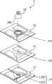
请参阅图1,图1为根据本发明一较佳具体实施例的按键1的组装分解透视图。如图1所示,按键1包括一基板10、一薄膜电路12、一第一绝缘层14、一第二绝缘层16、一弹性元件18、一键帽20以及一支撑装置22。Please refer to FIG. 1 . FIG. 1 is an exploded perspective view of a
如图1所示,薄膜电路12具有一开关120。在此具体实施例中,薄膜电路12大体上可由一聚对苯二甲酸乙二醇酯(Polyethylene Terephthalate,PET)所制成,但不以此为限。在此具体实施例中,开关120可包括一第一导电部分(conductive portion)1200以及一与第一导电部分1200分离的第二导电部分1202。换句话说,由于第一导电部分1200与第二导电部分1202为分离而无电性连接,故此时开关120处于关闭状态。在实际应用时,第一导电部分1200以及第二导电部分1202可被一碳胶(carbon paste)(未示于图中)披覆,该碳胶用以增加第一导电部分1200以及第二导电部分1202的耐磨性。As shown in FIG. 1 , the
如图1所示,第一绝缘层14形成于薄膜电路12上,第一绝缘层14具有一孔洞140,并且开关120暴露于孔洞140内。在此具体实施例中,第一绝缘层14是由一树脂(resin)所制成,其主要功能为绝缘,但不以此为限。此外,在此具体实施例中,第一绝缘层14可以一紫外线催化方法制造而成,但不以此为限。As shown in FIG. 1 , the first insulating
第二绝缘层16形成于第一绝缘层14上,第二绝缘层16具有一环形开口160,并且该环形开口160环绕第一绝缘层14的孔洞140。在此具体实施例中,第二绝缘层16是由一树脂所制成,具有绝缘的功能,但不以此为限。此外,在此具体实施例中,第二绝缘层16可以一热烤烘干方法制造而成,但不以此为限。在实际应用时,第二绝缘层16可具有一特定颜色,该特定颜色可与键帽20的一外观颜色相同或相配合,以达到美观的效果。The second insulating
请参阅图2以及图3,图2为图1中按键1的剖面视图。图3为图2中按键1的局部放大图。如图2以及图3所示,弹性元件18的一底部180可配合第二绝缘层16的环形开口160并且粘合至第二绝缘层16的环形开口160。弹性元件18可具有一接触部分182。弹性元件18大体上是由一橡胶(rubber)所制成,但不以此为限。在此具体实施例中,弹性元件18的底部180是利用一粘合剂(未示于图中)与环形开口160粘合,但不以此为限。在此具体实施例中,弹性元件18的形状可为圆顶体(dome),但不以此为限。Please refer to FIG. 2 and FIG. 3 , FIG. 2 is a cross-sectional view of the
在此具体实施例中,支撑装置22可活动地连接键帽20及基板10。支撑装置22可支撑键帽20做相对于该基板10垂直移动。当键帽20被一外力按压时,弹性元件18会变形,并且弹性元件18的接触部分182会接触开关120进而开启开关120。进一步来说,随着弹性元件18回应于键帽20的移动被压下,接触部分182同时接触第一导电部分1200以及第二导电部分1202以形成电性连接,进而开启开关120。In this embodiment, the supporting
借此,当弹性元18经由底部180件利用该粘合剂粘合至第二绝缘层16的环形开口160时,环形开口160可协助弹性元件18准确地粘合至一指定位置。此外,环形开口160亦可防止该粘合剂溢出环形开口160。Thereby, when the
请参阅图4,并且一并参阅图1至图3,图4为图1中按键1的制造方法的流程图。根据本发明一较佳具体实施例的制造方法,首先,执行步骤S10,制备一基板10。Please refer to FIG. 4 , and refer to FIGS. 1 to 3 together. FIG. 4 is a flow chart of the manufacturing method of the
接着,根据本发明一较佳具体实施例的制造方法执行步骤S12,制备一薄膜电路12。薄膜电路12具有一开关120。在此具体实施例中,薄膜电路12大体上可由一聚对苯二甲酸乙二醇酯所制成,但不以此为限。在此具体实施例中,开关120可包括一第一导电部分1200以及一与该第一导电部分1200分离的第二导电部分1202。换句话说,由于第一导电部分1200与第二导电部分1202为分离而无电性连接,故此时开关120处于关闭状态。在实际应用时,第一导电部分1200以及第二导电部分1202可被一碳胶(未示于图中)披覆,该碳胶用以增加第一导电部分1200以及第二导电部分1202的耐磨性。Next, the manufacturing method according to a preferred embodiment of the present invention executes step S12 to prepare a
然后,根据本发明一较佳具体实施例的制造方法执行步骤S14,在薄膜电路12上形成一第一绝缘层14。第一绝缘层14具有一孔洞140,并且120暴露于孔洞140内。在此具体实施例中,第一绝缘层14是由一树脂所制成,其主要功能为绝缘,但不以此为限。此外,在此具体实施例中,第一绝缘层14可以一紫外线催化方法制造而成,但不以此为限。Then, the manufacturing method according to a preferred embodiment of the present invention executes step S14 to form a first insulating
接着,根据本发明一较佳具体实施例的制造方法执行步骤S16,在第一绝缘层上14形成一第二绝缘层16。第二绝缘层16具有一环形开口160,并且该环形开口160环绕第一绝缘层14的孔洞140。在此具体实施例中,第二绝缘层16是由一树脂所制成,具有绝缘的功能,但不以此为限。此外,在此具体实施例中,第二绝缘层16可以一热烤烘干方法制造而成,但不以此为限。在实际应用时,第二绝缘层16可具有一特定颜色,该特定颜色可与键帽20的一外观颜色相同或相配合,以达到美观的效果。Next, the manufacturing method according to a preferred embodiment of the present invention executes step S16 to form a second insulating
之后,根据本发明一较佳具体实施例的制造方法执行步骤S18,制备一弹性元件18,并且弹性元件18的一底部180配合第二绝缘层16的环形开口160。在此具体实施例中,弹性元件18大体上是由一橡胶所制成,但不以此为限。Afterwards, the manufacturing method according to a preferred embodiment of the present invention executes step S18 to prepare an
然后,根据本发明一较佳具体实施例的制造方法执行步骤S20,利用一粘合剂粘合弹性元件18的底部180至第二绝缘层16的环形开口160。在此具体实施例中,环形开口160可协助弹性元件18准确地粘合至指定位置。此外,环形开口160亦可防止该粘合剂溢出环形开口160。Then, the manufacturing method according to a preferred embodiment of the present invention performs step S20 , using an adhesive to bond the bottom 180 of the
接着,根据本发明一较佳具体实施例的制造方法执行步骤S22,制备一键帽20。Next, the manufacturing method according to a preferred embodiment of the present invention executes step S22 to prepare a
之后,根据本发明一较佳具体实施例的制造方法执行步骤S24,制备一支撑装置22。于此实施例中,支撑装置22具有第一端220及第二端222。Afterwards, the manufacturing method according to a preferred embodiment of the present invention executes step S24 to prepare a supporting
最后,根据本发明一较佳具体实施例的制造方法执行步骤S26,将第一端220可活动地连接键帽20,并且将第二端22可活动地连接于基板10。Finally, the manufacturing method according to a preferred embodiment of the present invention executes step S26 , the
在此具体实施例中,弹性元件18可包括一接触部分182。当使用者施加一外力于键帽20,随着弹性元件18回应于键帽20的移动被压下,接触部分182同时接触第一导电部分1200以及第二导电1202部分以形成电性连接,进而开启开关120。In this embodiment, the
借此,当弹性元18经由底部180件利用该粘合剂粘合至第二绝缘层16的环形开口160时,环形开口160可协助弹性元件18准确地粘合至一指定位置。此外,环形开口160亦可防止该粘合剂溢出环形开口160。Thereby, when the
请参阅图5,图5为根据本发明一较佳具体实施例的薄膜开关电路2的组装分解透视图。在此较佳具体实施例中,薄膜开关电路2配合一弹性元件18。如图5所示,薄膜开关电路2包括一薄膜电路12、一第一绝缘层14以及一第二绝缘层16。Please refer to FIG. 5 . FIG. 5 is an assembled and exploded perspective view of the
如图5所示,薄膜电路12具有一开关120。在此具体实施例中,薄膜电路12大体上可由一聚对苯二甲酸乙二醇酯所制成,但不以此为限。在此具体实施例中,开关120可包括一第一导电部分1200以及一与第一导电部分1200分离的第二导电部分1202。换句话说,由于第一导电部分1200与第二导电部分1202为分离而无电性连接,故此时开关120处于关闭状态。在实际应用时,第一导电部分1200以及第二导电部分1202可被一碳胶(未示于图中)披覆,该碳胶用以增加第一导电部分1200以及第二导电部分1202的耐磨性。As shown in FIG. 5 , the
如图5所示,第一绝缘层14形成在薄膜电路12上,第一绝缘层14具有一孔洞140,并且开关120暴露于孔洞140内。在此具体实施例中,第一绝缘层14是由一树脂所制成,其主要功能为绝缘,但不以此为限。此外,在此具体实施例中,第一绝缘层14可以一紫外线催化方法制造而成,但不以此为限。As shown in FIG. 5 , the first insulating
第二绝缘层16形成于第一绝缘层14上,第二绝缘层16具有一环形开口160,并且该环形开口160环绕第一绝缘层14的孔洞140。在此具体实施例中,第二绝缘层16是由一树脂所制成,具有绝缘的功能,但不以此为限。此外,在此具体实施例中,第二绝缘层16可以一热烤烘干方法制造而成,但不以此为限。在实际应用时,第二绝缘层16可具有一特定颜色,以达到美观的效果。The second insulating
请参阅图6,图6为图5中薄膜开关电路2的剖面视图。在一具体实施例中,弹性元件180的一底部180是利用一粘合剂(未示于图中)粘合至第二绝缘层16的环形开口160。弹性元件18可具有一接触部分182。弹性元件18大体上是由一橡胶所制成,但不以此为限。在此具体实施例中,弹性元件18的底部180是利用一粘合剂(未示于图中)与环形开口160粘合,但不以此为限。在此具体实施例中,弹性元件18的形状可为圆顶体(dome),但不以此为限。Please refer to FIG. 6 , which is a cross-sectional view of the
在一具体实施例中,随着弹性元件18被压下,接触部分182同时接触第一导电部分1200以及第二导电部分1202以形成电性连接,进而开启开关120。In a specific embodiment, as the
借此,当弹性元18经由底部180件利用该粘合剂粘合至第二绝缘层16的环形开口160时,环形开口160可协助弹性元件18准确地粘合至一指定位置。此外,环形开口160亦可防止该粘合剂溢出环形开口160。Thereby, when the
请参阅图7,并且一并参阅图5以及图6,图7为根据图5中薄膜开关电路2的制造方法的流程图。在此具体实施例中,薄膜开关电路2配合一弹性元件18。根据本发明一较佳具体实施例的制造方法,首先,执行步骤S30,形成一薄膜电路12。薄膜电路12具有一开关120。在此具体实施例中,薄膜电路12大体上可由一聚对苯二甲酸乙二醇酯所制成,但不以此为限。Please refer to FIG. 7 , and refer to FIG. 5 and FIG. 6 together. FIG. 7 is a flow chart of the manufacturing method of the
在此具体实施例中,开关120可包括一第一导电部分1200以及一与该第一导电部分1200分离的第二导电部分1202。换句话说,由于第一导电部分1200与第二导电部分1202分离而无电性连接,故此时开关120处于关闭状态。在实际应用时,第一导电部分1200以及第二导电部分1202可被一碳胶披覆用以增加第一导电部分1200以及第二导电部分1202的耐磨性。In this embodiment, the
然后,根据本发明一较佳具体实施例的制造方法执行步骤S32,在薄膜电路12上形成一第一绝缘层14。第一绝缘层14具有一孔洞140,并且120暴露于孔洞140内。在此具体实施例中,第一绝缘层14是由一树脂所制成,其主要功能为绝缘,但不以此为限。此外,在此具体实施例中,第一绝缘层14可以一紫外线催化方法制造而成,但不以此为限。Then, the manufacturing method according to a preferred embodiment of the present invention executes step S32 to form a first insulating
接着,根据本发明一较佳具体实施例的制造方法执行步骤S34,在第一绝缘层上14形成一第二绝缘层16。第二绝缘层16具有一环形开口160,并且该环形开口160环绕第一绝缘层14的孔洞140。在此具体实施例中,第二绝缘层16是由一树脂(resin)所制成,具有绝缘的功能,但不以此为限。此外,在此具体实施例中,第二绝缘层16可以一热烤烘干方法制造而成,但不以此为限。在实际应用时,第二绝缘层16可具有一特定颜色,以达到美观的效果。Next, the manufacturing method according to a preferred embodiment of the present invention executes step S34 to form a second insulating
然后,根据本发明一较佳具体实施例的制造方法执行步骤S36,利用一粘合剂粘合弹性元件18的底部180至第二绝缘层16的环形开口160。在此具体实施例中,环形开口160可协助弹性元件18准确地粘合至指定位置。此外,环形开口160亦可防止该粘合剂溢出环形开口160。在此具体实施例中,弹性元件18大体上是由一橡胶所制成,但不以此为限。Then, the manufacturing method according to a preferred embodiment of the present invention executes step S36 , using an adhesive to bond the bottom 180 of the
在此具体实施例中,弹性元件18可包括一接触部分182。随着弹性元件18被压下,接触部分182同时接触第一导电部分1200以及第二导电1202部分以形成电性连接,进而开启开关120。In this embodiment, the
相较于先前技术,根据本发明的按键以及薄膜电路开关,当该弹性元件利用一粘合剂粘合至该薄膜开关电路时,该环形开口可协助该弹性元件准确地粘合至指定位置。此外,该环形开口可防止该粘合剂溢出该环形开口。借此,在该按键的制造过程中,该弹性元件的粘合将更为准确,进而增加该按键的制造品质以及产品良品率。Compared with the prior art, according to the button and the membrane circuit switch of the present invention, when the elastic element is bonded to the membrane switch circuit by an adhesive, the annular opening can help the elastic element to be adhered to the designated position accurately. Furthermore, the annular opening prevents the adhesive from overflowing the annular opening. Thereby, during the manufacturing process of the button, the bonding of the elastic element will be more accurate, thereby increasing the manufacturing quality and product yield of the button.
借由以上较佳具体实施例的详述,希望能更加清楚描述本发明的特征与精神,而并非以上述所公开的较佳具体实施例来对本发明的范畴加以限制。相反地,其目的是希望能涵盖各种改变及具相等性的安排于本发明的范畴内。因此,本发明的范畴应该根据上述的说明作最宽广的解释,以致使其涵盖所有可能的改变以及具相等性的安排。By virtue of the above detailed description of the preferred embodiments, it is hoped that the features and spirit of the present invention can be described more clearly, and the scope of the present invention is not limited by the preferred embodiments disclosed above. On the contrary, the intention is to cover various modifications and equivalent arrangements within the scope of the invention. Therefore, the scope of the present invention should be construed in the broadest way based on the above description so as to cover all possible modifications and equivalent arrangements.
Claims (38)
Priority Applications (1)
| Application Number | Priority Date | Filing Date | Title |
|---|---|---|---|
| CN2007101064123ACN101315841B (en) | 2007-05-29 | 2007-05-29 | Key using membrane switch circuit and manufacturing method thereof |
Applications Claiming Priority (1)
| Application Number | Priority Date | Filing Date | Title |
|---|---|---|---|
| CN2007101064123ACN101315841B (en) | 2007-05-29 | 2007-05-29 | Key using membrane switch circuit and manufacturing method thereof |
Publications (2)
| Publication Number | Publication Date |
|---|---|
| CN101315841Atrue CN101315841A (en) | 2008-12-03 |
| CN101315841B CN101315841B (en) | 2011-12-07 |
Family
ID=40106795
Family Applications (1)
| Application Number | Title | Priority Date | Filing Date |
|---|---|---|---|
| CN2007101064123AExpired - Fee RelatedCN101315841B (en) | 2007-05-29 | 2007-05-29 | Key using membrane switch circuit and manufacturing method thereof |
Country Status (1)
| Country | Link |
|---|---|
| CN (1) | CN101315841B (en) |
Cited By (29)
| Publication number | Priority date | Publication date | Assignee | Title |
|---|---|---|---|---|
| CN101599379B (en)* | 2009-06-03 | 2012-01-04 | 珠海市智迪科技有限公司 | Key lifting switch device and assembling fixture and assembling technology thereof |
| CN104035571A (en)* | 2014-05-19 | 2014-09-10 | 苏州达方电子有限公司 | Keyboard capable of detecting contact force and method applied to keyboard for detecting contact force |
| US9704665B2 (en) | 2014-05-19 | 2017-07-11 | Apple Inc. | Backlit keyboard including reflective component |
| US9704670B2 (en) | 2013-09-30 | 2017-07-11 | Apple Inc. | Keycaps having reduced thickness |
| US9710069B2 (en) | 2012-10-30 | 2017-07-18 | Apple Inc. | Flexible printed circuit having flex tails upon which keyboard keycaps are coupled |
| US9715978B2 (en) | 2014-05-27 | 2017-07-25 | Apple Inc. | Low travel switch assembly |
| US9761389B2 (en) | 2012-10-30 | 2017-09-12 | Apple Inc. | Low-travel key mechanisms with butterfly hinges |
| US9779889B2 (en) | 2014-03-24 | 2017-10-03 | Apple Inc. | Scissor mechanism features for a keyboard |
| US9793066B1 (en) | 2014-01-31 | 2017-10-17 | Apple Inc. | Keyboard hinge mechanism |
| US9870880B2 (en) | 2014-09-30 | 2018-01-16 | Apple Inc. | Dome switch and switch housing for keyboard assembly |
| US9908310B2 (en) | 2013-07-10 | 2018-03-06 | Apple Inc. | Electronic device with a reduced friction surface |
| CN107787140A (en)* | 2016-08-25 | 2018-03-09 | 纬创资通股份有限公司 | Electronic device and pressure sensing piece thereof |
| US9916945B2 (en) | 2012-10-30 | 2018-03-13 | Apple Inc. | Low-travel key mechanisms using butterfly hinges |
| US9927895B2 (en) | 2013-02-06 | 2018-03-27 | Apple Inc. | Input/output device with a dynamically adjustable appearance and function |
| US9934915B2 (en) | 2015-06-10 | 2018-04-03 | Apple Inc. | Reduced layer keyboard stack-up |
| US9971084B2 (en) | 2015-09-28 | 2018-05-15 | Apple Inc. | Illumination structure for uniform illumination of keys |
| US9997304B2 (en) | 2015-05-13 | 2018-06-12 | Apple Inc. | Uniform illumination of keys |
| US9997308B2 (en) | 2015-05-13 | 2018-06-12 | Apple Inc. | Low-travel key mechanism for an input device |
| US10002727B2 (en) | 2013-09-30 | 2018-06-19 | Apple Inc. | Keycaps with reduced thickness |
| US10083805B2 (en) | 2015-05-13 | 2018-09-25 | Apple Inc. | Keyboard for electronic device |
| US10082880B1 (en) | 2014-08-28 | 2018-09-25 | Apple Inc. | System level features of a keyboard |
| US10115544B2 (en) | 2016-08-08 | 2018-10-30 | Apple Inc. | Singulated keyboard assemblies and methods for assembling a keyboard |
| US10128064B2 (en) | 2015-05-13 | 2018-11-13 | Apple Inc. | Keyboard assemblies having reduced thicknesses and method of forming keyboard assemblies |
| US10262814B2 (en) | 2013-05-27 | 2019-04-16 | Apple Inc. | Low travel switch assembly |
| US10353485B1 (en) | 2016-07-27 | 2019-07-16 | Apple Inc. | Multifunction input device with an embedded capacitive sensing layer |
| US10755877B1 (en) | 2016-08-29 | 2020-08-25 | Apple Inc. | Keyboard for an electronic device |
| US10775850B2 (en) | 2017-07-26 | 2020-09-15 | Apple Inc. | Computer with keyboard |
| US10796863B2 (en) | 2014-08-15 | 2020-10-06 | Apple Inc. | Fabric keyboard |
| US11500538B2 (en) | 2016-09-13 | 2022-11-15 | Apple Inc. | Keyless keyboard with force sensing and haptic feedback |
Family Cites Families (3)
| Publication number | Priority date | Publication date | Assignee | Title |
|---|---|---|---|---|
| US6366275B1 (en)* | 2000-01-21 | 2002-04-02 | Behavior Tech Computer Corporation | Push button structure of keyboard |
| CN2603493Y (en)* | 2003-02-21 | 2004-02-11 | 东莞大洋硅胶制品有限公司 | a button |
| US6880995B2 (en)* | 2003-07-09 | 2005-04-19 | Monterey International Corp. | Elastic-cup support for computer keyboard |
- 2007
- 2007-05-29CNCN2007101064123Apatent/CN101315841B/ennot_activeExpired - Fee Related
Cited By (47)
| Publication number | Priority date | Publication date | Assignee | Title |
|---|---|---|---|---|
| CN101599379B (en)* | 2009-06-03 | 2012-01-04 | 珠海市智迪科技有限公司 | Key lifting switch device and assembling fixture and assembling technology thereof |
| US9916945B2 (en) | 2012-10-30 | 2018-03-13 | Apple Inc. | Low-travel key mechanisms using butterfly hinges |
| US10699856B2 (en) | 2012-10-30 | 2020-06-30 | Apple Inc. | Low-travel key mechanisms using butterfly hinges |
| US11023081B2 (en) | 2012-10-30 | 2021-06-01 | Apple Inc. | Multi-functional keyboard assemblies |
| US9710069B2 (en) | 2012-10-30 | 2017-07-18 | Apple Inc. | Flexible printed circuit having flex tails upon which keyboard keycaps are coupled |
| US10254851B2 (en) | 2012-10-30 | 2019-04-09 | Apple Inc. | Keyboard key employing a capacitive sensor and dome |
| US9761389B2 (en) | 2012-10-30 | 2017-09-12 | Apple Inc. | Low-travel key mechanisms with butterfly hinges |
| US10211008B2 (en) | 2012-10-30 | 2019-02-19 | Apple Inc. | Low-travel key mechanisms using butterfly hinges |
| US9927895B2 (en) | 2013-02-06 | 2018-03-27 | Apple Inc. | Input/output device with a dynamically adjustable appearance and function |
| US10114489B2 (en) | 2013-02-06 | 2018-10-30 | Apple Inc. | Input/output device with a dynamically adjustable appearance and function |
| US10262814B2 (en) | 2013-05-27 | 2019-04-16 | Apple Inc. | Low travel switch assembly |
| US9908310B2 (en) | 2013-07-10 | 2018-03-06 | Apple Inc. | Electronic device with a reduced friction surface |
| US10556408B2 (en) | 2013-07-10 | 2020-02-11 | Apple Inc. | Electronic device with a reduced friction surface |
| US10224157B2 (en) | 2013-09-30 | 2019-03-05 | Apple Inc. | Keycaps having reduced thickness |
| US9704670B2 (en) | 2013-09-30 | 2017-07-11 | Apple Inc. | Keycaps having reduced thickness |
| US10804051B2 (en) | 2013-09-30 | 2020-10-13 | Apple Inc. | Keycaps having reduced thickness |
| US11699558B2 (en) | 2013-09-30 | 2023-07-11 | Apple Inc. | Keycaps having reduced thickness |
| US10002727B2 (en) | 2013-09-30 | 2018-06-19 | Apple Inc. | Keycaps with reduced thickness |
| US9793066B1 (en) | 2014-01-31 | 2017-10-17 | Apple Inc. | Keyboard hinge mechanism |
| US9779889B2 (en) | 2014-03-24 | 2017-10-03 | Apple Inc. | Scissor mechanism features for a keyboard |
| CN104035571A (en)* | 2014-05-19 | 2014-09-10 | 苏州达方电子有限公司 | Keyboard capable of detecting contact force and method applied to keyboard for detecting contact force |
| US9704665B2 (en) | 2014-05-19 | 2017-07-11 | Apple Inc. | Backlit keyboard including reflective component |
| US9715978B2 (en) | 2014-05-27 | 2017-07-25 | Apple Inc. | Low travel switch assembly |
| US10796863B2 (en) | 2014-08-15 | 2020-10-06 | Apple Inc. | Fabric keyboard |
| US10082880B1 (en) | 2014-08-28 | 2018-09-25 | Apple Inc. | System level features of a keyboard |
| US9870880B2 (en) | 2014-09-30 | 2018-01-16 | Apple Inc. | Dome switch and switch housing for keyboard assembly |
| US10128061B2 (en) | 2014-09-30 | 2018-11-13 | Apple Inc. | Key and switch housing for keyboard assembly |
| US10192696B2 (en) | 2014-09-30 | 2019-01-29 | Apple Inc. | Light-emitting assembly for keyboard |
| US10134539B2 (en) | 2014-09-30 | 2018-11-20 | Apple Inc. | Venting system and shield for keyboard |
| US10468211B2 (en) | 2015-05-13 | 2019-11-05 | Apple Inc. | Illuminated low-travel key mechanism for a keyboard |
| US10083806B2 (en) | 2015-05-13 | 2018-09-25 | Apple Inc. | Keyboard for electronic device |
| US10083805B2 (en) | 2015-05-13 | 2018-09-25 | Apple Inc. | Keyboard for electronic device |
| US9997308B2 (en) | 2015-05-13 | 2018-06-12 | Apple Inc. | Low-travel key mechanism for an input device |
| US10424446B2 (en) | 2015-05-13 | 2019-09-24 | Apple Inc. | Keyboard assemblies having reduced thickness and method of forming keyboard assemblies |
| US10128064B2 (en) | 2015-05-13 | 2018-11-13 | Apple Inc. | Keyboard assemblies having reduced thicknesses and method of forming keyboard assemblies |
| US9997304B2 (en) | 2015-05-13 | 2018-06-12 | Apple Inc. | Uniform illumination of keys |
| US9934915B2 (en) | 2015-06-10 | 2018-04-03 | Apple Inc. | Reduced layer keyboard stack-up |
| US10310167B2 (en) | 2015-09-28 | 2019-06-04 | Apple Inc. | Illumination structure for uniform illumination of keys |
| US9971084B2 (en) | 2015-09-28 | 2018-05-15 | Apple Inc. | Illumination structure for uniform illumination of keys |
| US10353485B1 (en) | 2016-07-27 | 2019-07-16 | Apple Inc. | Multifunction input device with an embedded capacitive sensing layer |
| US10115544B2 (en) | 2016-08-08 | 2018-10-30 | Apple Inc. | Singulated keyboard assemblies and methods for assembling a keyboard |
| US11282659B2 (en) | 2016-08-08 | 2022-03-22 | Apple Inc. | Singulated keyboard assemblies and methods for assembling a keyboard |
| CN107787140B (en)* | 2016-08-25 | 2020-03-03 | 纬创资通股份有限公司 | Electronic device and pressure sensing piece thereof |
| CN107787140A (en)* | 2016-08-25 | 2018-03-09 | 纬创资通股份有限公司 | Electronic device and pressure sensing piece thereof |
| US10755877B1 (en) | 2016-08-29 | 2020-08-25 | Apple Inc. | Keyboard for an electronic device |
| US11500538B2 (en) | 2016-09-13 | 2022-11-15 | Apple Inc. | Keyless keyboard with force sensing and haptic feedback |
| US10775850B2 (en) | 2017-07-26 | 2020-09-15 | Apple Inc. | Computer with keyboard |
Also Published As
| Publication number | Publication date |
|---|---|
| CN101315841B (en) | 2011-12-07 |
Similar Documents
| Publication | Publication Date | Title |
|---|---|---|
| CN101315841A (en) | Key using membrane switch circuit and manufacturing method thereof | |
| CN201123174Y (en) | Thin film switch circuit and key using same | |
| EP2340548B1 (en) | Dome sheet and key pad | |
| CN100424798C (en) | Movable contact body and panel switch using the same | |
| JP4936323B2 (en) | Operation switch sheet member, operation switch, and method of manufacturing operation switch sheet member | |
| JP5566536B2 (en) | PCB tact switch | |
| JP4898323B2 (en) | Key sheet and push button switch | |
| JP2002056737A (en) | Illumination-type switch | |
| TWI343063B (en) | A method for manufacturing a switch sheet | |
| US20070144873A1 (en) | Watertight key switch assembly and its fabrication | |
| WO2018040825A1 (en) | Soft rubber keyboard with hard sheet bonded to bottom portion thereof | |
| JP5194764B2 (en) | Movable contact body and manufacturing method thereof | |
| TWM324842U (en) | Membrane switch circuit and keyswitch using such membrane switch circuit | |
| KR101038622B1 (en) | A PCB tact switch | |
| CN101206964A (en) | Movable contact body and switch using it | |
| US7186939B2 (en) | Movable contact unit and panel switch | |
| US8803016B2 (en) | Dome sheet structure including light guide film and mobile communication terminal including the dome sheet structure | |
| JP2004186020A (en) | Movable contact body with operation protrusion, method of mounting operation protrusion, and switch for operation panel using the same | |
| US7164089B2 (en) | Thin keyboard structure | |
| US20130341170A1 (en) | Key membrane and electronic device using the same | |
| JP2007123231A (en) | Cover member for push-button switch | |
| JPH10125172A (en) | Push button switch member | |
| TWI306267B (en) | Keyswitch using membrane switch circuit and method of making the same | |
| JP2011243555A (en) | Keypad plunger structure and method of manufacturing the same | |
| JP2009193905A (en) | Panel switch |
Legal Events
| Date | Code | Title | Description |
|---|---|---|---|
| C06 | Publication | ||
| PB01 | Publication | ||
| C10 | Entry into substantive examination | ||
| SE01 | Entry into force of request for substantive examination | ||
| C14 | Grant of patent or utility model | ||
| GR01 | Patent grant | ||
| C17 | Cessation of patent right | ||
| CF01 | Termination of patent right due to non-payment of annual fee | Granted publication date:20111207 Termination date:20130529 |