CN101312185A - Light emitting device and method for manufacturing the same - Google Patents
Light emitting device and method for manufacturing the sameDownload PDFInfo
- Publication number
- CN101312185A CN101312185ACNA2008101314744ACN200810131474ACN101312185ACN 101312185 ACN101312185 ACN 101312185ACN A2008101314744 ACNA2008101314744 ACN A2008101314744ACN 200810131474 ACN200810131474 ACN 200810131474ACN 101312185 ACN101312185 ACN 101312185A
- Authority
- CN
- China
- Prior art keywords
- light
- emitting device
- sealing body
- light emitting
- body layer
- Prior art date
- Legal status (The legal status is an assumption and is not a legal conclusion. Google has not performed a legal analysis and makes no representation as to the accuracy of the status listed.)
- Granted
Links
Images


Classifications
- H—ELECTRICITY
- H01—ELECTRIC ELEMENTS
- H01B—CABLES; CONDUCTORS; INSULATORS; SELECTION OF MATERIALS FOR THEIR CONDUCTIVE, INSULATING OR DIELECTRIC PROPERTIES
- H01B1/00—Conductors or conductive bodies characterised by the conductive materials; Selection of materials as conductors
- H01B1/06—Conductors or conductive bodies characterised by the conductive materials; Selection of materials as conductors mainly consisting of other non-metallic substances
- H01B1/10—Conductors or conductive bodies characterised by the conductive materials; Selection of materials as conductors mainly consisting of other non-metallic substances sulfides
- F—MECHANICAL ENGINEERING; LIGHTING; HEATING; WEAPONS; BLASTING
- F21—LIGHTING
- F21K—NON-ELECTRIC LIGHT SOURCES USING LUMINESCENCE; LIGHT SOURCES USING ELECTROCHEMILUMINESCENCE; LIGHT SOURCES USING CHARGES OF COMBUSTIBLE MATERIAL; LIGHT SOURCES USING SEMICONDUCTOR DEVICES AS LIGHT-GENERATING ELEMENTS; LIGHT SOURCES NOT OTHERWISE PROVIDED FOR
- F21K9/00—Light sources using semiconductor devices as light-generating elements, e.g. using light-emitting diodes [LED] or lasers
- F21K9/20—Light sources comprising attachment means
- F21K9/23—Retrofit light sources for lighting devices with a single fitting for each light source, e.g. for substitution of incandescent lamps with bayonet or threaded fittings
- F21K9/232—Retrofit light sources for lighting devices with a single fitting for each light source, e.g. for substitution of incandescent lamps with bayonet or threaded fittings specially adapted for generating an essentially omnidirectional light distribution, e.g. with a glass bulb
- F—MECHANICAL ENGINEERING; LIGHTING; HEATING; WEAPONS; BLASTING
- F21—LIGHTING
- F21Y—INDEXING SCHEME ASSOCIATED WITH SUBCLASSES F21K, F21L, F21S and F21V, RELATING TO THE FORM OR THE KIND OF THE LIGHT SOURCES OR OF THE COLOUR OF THE LIGHT EMITTED
- F21Y2115/00—Light-generating elements of semiconductor light sources
- F21Y2115/10—Light-emitting diodes [LED]
- H—ELECTRICITY
- H01—ELECTRIC ELEMENTS
- H01L—SEMICONDUCTOR DEVICES NOT COVERED BY CLASS H10
- H01L2224/00—Indexing scheme for arrangements for connecting or disconnecting semiconductor or solid-state bodies and methods related thereto as covered by H01L24/00
- H01L2224/01—Means for bonding being attached to, or being formed on, the surface to be connected, e.g. chip-to-package, die-attach, "first-level" interconnects; Manufacturing methods related thereto
- H01L2224/26—Layer connectors, e.g. plate connectors, solder or adhesive layers; Manufacturing methods related thereto
- H01L2224/31—Structure, shape, material or disposition of the layer connectors after the connecting process
- H01L2224/32—Structure, shape, material or disposition of the layer connectors after the connecting process of an individual layer connector
- H01L2224/321—Disposition
- H01L2224/32151—Disposition the layer connector connecting between a semiconductor or solid-state body and an item not being a semiconductor or solid-state body, e.g. chip-to-substrate, chip-to-passive
- H01L2224/32221—Disposition the layer connector connecting between a semiconductor or solid-state body and an item not being a semiconductor or solid-state body, e.g. chip-to-substrate, chip-to-passive the body and the item being stacked
- H01L2224/32225—Disposition the layer connector connecting between a semiconductor or solid-state body and an item not being a semiconductor or solid-state body, e.g. chip-to-substrate, chip-to-passive the body and the item being stacked the item being non-metallic, e.g. insulating substrate with or without metallisation
- H—ELECTRICITY
- H01—ELECTRIC ELEMENTS
- H01L—SEMICONDUCTOR DEVICES NOT COVERED BY CLASS H10
- H01L2224/00—Indexing scheme for arrangements for connecting or disconnecting semiconductor or solid-state bodies and methods related thereto as covered by H01L24/00
- H01L2224/01—Means for bonding being attached to, or being formed on, the surface to be connected, e.g. chip-to-package, die-attach, "first-level" interconnects; Manufacturing methods related thereto
- H01L2224/42—Wire connectors; Manufacturing methods related thereto
- H01L2224/44—Structure, shape, material or disposition of the wire connectors prior to the connecting process
- H01L2224/45—Structure, shape, material or disposition of the wire connectors prior to the connecting process of an individual wire connector
- H01L2224/45001—Core members of the connector
- H01L2224/45099—Material
- H01L2224/451—Material with a principal constituent of the material being a metal or a metalloid, e.g. boron (B), silicon (Si), germanium (Ge), arsenic (As), antimony (Sb), tellurium (Te) and polonium (Po), and alloys thereof
- H01L2224/45117—Material with a principal constituent of the material being a metal or a metalloid, e.g. boron (B), silicon (Si), germanium (Ge), arsenic (As), antimony (Sb), tellurium (Te) and polonium (Po), and alloys thereof the principal constituent melting at a temperature of greater than or equal to 400°C and less than 950°C
- H01L2224/45124—Aluminium (Al) as principal constituent
- H—ELECTRICITY
- H01—ELECTRIC ELEMENTS
- H01L—SEMICONDUCTOR DEVICES NOT COVERED BY CLASS H10
- H01L2224/00—Indexing scheme for arrangements for connecting or disconnecting semiconductor or solid-state bodies and methods related thereto as covered by H01L24/00
- H01L2224/01—Means for bonding being attached to, or being formed on, the surface to be connected, e.g. chip-to-package, die-attach, "first-level" interconnects; Manufacturing methods related thereto
- H01L2224/42—Wire connectors; Manufacturing methods related thereto
- H01L2224/44—Structure, shape, material or disposition of the wire connectors prior to the connecting process
- H01L2224/45—Structure, shape, material or disposition of the wire connectors prior to the connecting process of an individual wire connector
- H01L2224/45001—Core members of the connector
- H01L2224/45099—Material
- H01L2224/451—Material with a principal constituent of the material being a metal or a metalloid, e.g. boron (B), silicon (Si), germanium (Ge), arsenic (As), antimony (Sb), tellurium (Te) and polonium (Po), and alloys thereof
- H01L2224/45138—Material with a principal constituent of the material being a metal or a metalloid, e.g. boron (B), silicon (Si), germanium (Ge), arsenic (As), antimony (Sb), tellurium (Te) and polonium (Po), and alloys thereof the principal constituent melting at a temperature of greater than or equal to 950°C and less than 1550°C
- H01L2224/45144—Gold (Au) as principal constituent
- H—ELECTRICITY
- H01—ELECTRIC ELEMENTS
- H01L—SEMICONDUCTOR DEVICES NOT COVERED BY CLASS H10
- H01L2224/00—Indexing scheme for arrangements for connecting or disconnecting semiconductor or solid-state bodies and methods related thereto as covered by H01L24/00
- H01L2224/01—Means for bonding being attached to, or being formed on, the surface to be connected, e.g. chip-to-package, die-attach, "first-level" interconnects; Manufacturing methods related thereto
- H01L2224/42—Wire connectors; Manufacturing methods related thereto
- H01L2224/44—Structure, shape, material or disposition of the wire connectors prior to the connecting process
- H01L2224/45—Structure, shape, material or disposition of the wire connectors prior to the connecting process of an individual wire connector
- H01L2224/45001—Core members of the connector
- H01L2224/45099—Material
- H01L2224/451—Material with a principal constituent of the material being a metal or a metalloid, e.g. boron (B), silicon (Si), germanium (Ge), arsenic (As), antimony (Sb), tellurium (Te) and polonium (Po), and alloys thereof
- H01L2224/45138—Material with a principal constituent of the material being a metal or a metalloid, e.g. boron (B), silicon (Si), germanium (Ge), arsenic (As), antimony (Sb), tellurium (Te) and polonium (Po), and alloys thereof the principal constituent melting at a temperature of greater than or equal to 950°C and less than 1550°C
- H01L2224/45147—Copper (Cu) as principal constituent
- H—ELECTRICITY
- H01—ELECTRIC ELEMENTS
- H01L—SEMICONDUCTOR DEVICES NOT COVERED BY CLASS H10
- H01L2224/00—Indexing scheme for arrangements for connecting or disconnecting semiconductor or solid-state bodies and methods related thereto as covered by H01L24/00
- H01L2224/01—Means for bonding being attached to, or being formed on, the surface to be connected, e.g. chip-to-package, die-attach, "first-level" interconnects; Manufacturing methods related thereto
- H01L2224/42—Wire connectors; Manufacturing methods related thereto
- H01L2224/44—Structure, shape, material or disposition of the wire connectors prior to the connecting process
- H01L2224/45—Structure, shape, material or disposition of the wire connectors prior to the connecting process of an individual wire connector
- H01L2224/45001—Core members of the connector
- H01L2224/45099—Material
- H01L2224/451—Material with a principal constituent of the material being a metal or a metalloid, e.g. boron (B), silicon (Si), germanium (Ge), arsenic (As), antimony (Sb), tellurium (Te) and polonium (Po), and alloys thereof
- H01L2224/45163—Material with a principal constituent of the material being a metal or a metalloid, e.g. boron (B), silicon (Si), germanium (Ge), arsenic (As), antimony (Sb), tellurium (Te) and polonium (Po), and alloys thereof the principal constituent melting at a temperature of greater than 1550°C
- H01L2224/45169—Platinum (Pt) as principal constituent
- H—ELECTRICITY
- H01—ELECTRIC ELEMENTS
- H01L—SEMICONDUCTOR DEVICES NOT COVERED BY CLASS H10
- H01L2224/00—Indexing scheme for arrangements for connecting or disconnecting semiconductor or solid-state bodies and methods related thereto as covered by H01L24/00
- H01L2224/01—Means for bonding being attached to, or being formed on, the surface to be connected, e.g. chip-to-package, die-attach, "first-level" interconnects; Manufacturing methods related thereto
- H01L2224/42—Wire connectors; Manufacturing methods related thereto
- H01L2224/47—Structure, shape, material or disposition of the wire connectors after the connecting process
- H01L2224/48—Structure, shape, material or disposition of the wire connectors after the connecting process of an individual wire connector
- H01L2224/4805—Shape
- H01L2224/4809—Loop shape
- H01L2224/48091—Arched
- H—ELECTRICITY
- H01—ELECTRIC ELEMENTS
- H01L—SEMICONDUCTOR DEVICES NOT COVERED BY CLASS H10
- H01L2224/00—Indexing scheme for arrangements for connecting or disconnecting semiconductor or solid-state bodies and methods related thereto as covered by H01L24/00
- H01L2224/01—Means for bonding being attached to, or being formed on, the surface to be connected, e.g. chip-to-package, die-attach, "first-level" interconnects; Manufacturing methods related thereto
- H01L2224/42—Wire connectors; Manufacturing methods related thereto
- H01L2224/47—Structure, shape, material or disposition of the wire connectors after the connecting process
- H01L2224/48—Structure, shape, material or disposition of the wire connectors after the connecting process of an individual wire connector
- H01L2224/481—Disposition
- H01L2224/48151—Connecting between a semiconductor or solid-state body and an item not being a semiconductor or solid-state body, e.g. chip-to-substrate, chip-to-passive
- H01L2224/48221—Connecting between a semiconductor or solid-state body and an item not being a semiconductor or solid-state body, e.g. chip-to-substrate, chip-to-passive the body and the item being stacked
- H01L2224/48225—Connecting between a semiconductor or solid-state body and an item not being a semiconductor or solid-state body, e.g. chip-to-substrate, chip-to-passive the body and the item being stacked the item being non-metallic, e.g. insulating substrate with or without metallisation
- H01L2224/48227—Connecting between a semiconductor or solid-state body and an item not being a semiconductor or solid-state body, e.g. chip-to-substrate, chip-to-passive the body and the item being stacked the item being non-metallic, e.g. insulating substrate with or without metallisation connecting the wire to a bond pad of the item
- H—ELECTRICITY
- H01—ELECTRIC ELEMENTS
- H01L—SEMICONDUCTOR DEVICES NOT COVERED BY CLASS H10
- H01L2224/00—Indexing scheme for arrangements for connecting or disconnecting semiconductor or solid-state bodies and methods related thereto as covered by H01L24/00
- H01L2224/73—Means for bonding being of different types provided for in two or more of groups H01L2224/10, H01L2224/18, H01L2224/26, H01L2224/34, H01L2224/42, H01L2224/50, H01L2224/63, H01L2224/71
- H01L2224/732—Location after the connecting process
- H01L2224/73251—Location after the connecting process on different surfaces
- H01L2224/73265—Layer and wire connectors
- H—ELECTRICITY
- H01—ELECTRIC ELEMENTS
- H01L—SEMICONDUCTOR DEVICES NOT COVERED BY CLASS H10
- H01L24/00—Arrangements for connecting or disconnecting semiconductor or solid-state bodies; Methods or apparatus related thereto
- H01L24/01—Means for bonding being attached to, or being formed on, the surface to be connected, e.g. chip-to-package, die-attach, "first-level" interconnects; Manufacturing methods related thereto
- H01L24/42—Wire connectors; Manufacturing methods related thereto
- H01L24/44—Structure, shape, material or disposition of the wire connectors prior to the connecting process
- H01L24/45—Structure, shape, material or disposition of the wire connectors prior to the connecting process of an individual wire connector
- H—ELECTRICITY
- H01—ELECTRIC ELEMENTS
- H01L—SEMICONDUCTOR DEVICES NOT COVERED BY CLASS H10
- H01L24/00—Arrangements for connecting or disconnecting semiconductor or solid-state bodies; Methods or apparatus related thereto
- H01L24/73—Means for bonding being of different types provided for in two or more of groups H01L24/10, H01L24/18, H01L24/26, H01L24/34, H01L24/42, H01L24/50, H01L24/63, H01L24/71
- H—ELECTRICITY
- H01—ELECTRIC ELEMENTS
- H01L—SEMICONDUCTOR DEVICES NOT COVERED BY CLASS H10
- H01L25/00—Assemblies consisting of a plurality of semiconductor or other solid state devices
- H01L25/03—Assemblies consisting of a plurality of semiconductor or other solid state devices all the devices being of a type provided for in a single subclass of subclasses H10B, H10D, H10F, H10H, H10K or H10N, e.g. assemblies of rectifier diodes
- H01L25/04—Assemblies consisting of a plurality of semiconductor or other solid state devices all the devices being of a type provided for in a single subclass of subclasses H10B, H10D, H10F, H10H, H10K or H10N, e.g. assemblies of rectifier diodes the devices not having separate containers
- H01L25/075—Assemblies consisting of a plurality of semiconductor or other solid state devices all the devices being of a type provided for in a single subclass of subclasses H10B, H10D, H10F, H10H, H10K or H10N, e.g. assemblies of rectifier diodes the devices not having separate containers the devices being of a type provided for in group H10H20/00
- H01L25/0753—Assemblies consisting of a plurality of semiconductor or other solid state devices all the devices being of a type provided for in a single subclass of subclasses H10B, H10D, H10F, H10H, H10K or H10N, e.g. assemblies of rectifier diodes the devices not having separate containers the devices being of a type provided for in group H10H20/00 the devices being arranged next to each other
- H—ELECTRICITY
- H01—ELECTRIC ELEMENTS
- H01L—SEMICONDUCTOR DEVICES NOT COVERED BY CLASS H10
- H01L2924/00—Indexing scheme for arrangements or methods for connecting or disconnecting semiconductor or solid-state bodies as covered by H01L24/00
- H01L2924/01—Chemical elements
- H01L2924/01015—Phosphorus [P]
- H—ELECTRICITY
- H01—ELECTRIC ELEMENTS
- H01L—SEMICONDUCTOR DEVICES NOT COVERED BY CLASS H10
- H01L2924/00—Indexing scheme for arrangements or methods for connecting or disconnecting semiconductor or solid-state bodies as covered by H01L24/00
- H01L2924/01—Chemical elements
- H01L2924/0102—Calcium [Ca]
- H—ELECTRICITY
- H01—ELECTRIC ELEMENTS
- H01L—SEMICONDUCTOR DEVICES NOT COVERED BY CLASS H10
- H01L2924/00—Indexing scheme for arrangements or methods for connecting or disconnecting semiconductor or solid-state bodies as covered by H01L24/00
- H01L2924/01—Chemical elements
- H01L2924/01047—Silver [Ag]
- H—ELECTRICITY
- H01—ELECTRIC ELEMENTS
- H01L—SEMICONDUCTOR DEVICES NOT COVERED BY CLASS H10
- H01L2924/00—Indexing scheme for arrangements or methods for connecting or disconnecting semiconductor or solid-state bodies as covered by H01L24/00
- H01L2924/01—Chemical elements
- H01L2924/01063—Europium [Eu]
- H—ELECTRICITY
- H01—ELECTRIC ELEMENTS
- H01L—SEMICONDUCTOR DEVICES NOT COVERED BY CLASS H10
- H01L2924/00—Indexing scheme for arrangements or methods for connecting or disconnecting semiconductor or solid-state bodies as covered by H01L24/00
- H01L2924/01—Chemical elements
- H01L2924/01078—Platinum [Pt]
- H—ELECTRICITY
- H01—ELECTRIC ELEMENTS
- H01L—SEMICONDUCTOR DEVICES NOT COVERED BY CLASS H10
- H01L2924/00—Indexing scheme for arrangements or methods for connecting or disconnecting semiconductor or solid-state bodies as covered by H01L24/00
- H01L2924/01—Chemical elements
- H01L2924/01079—Gold [Au]
- H—ELECTRICITY
- H01—ELECTRIC ELEMENTS
- H01L—SEMICONDUCTOR DEVICES NOT COVERED BY CLASS H10
- H01L2924/00—Indexing scheme for arrangements or methods for connecting or disconnecting semiconductor or solid-state bodies as covered by H01L24/00
- H01L2924/10—Details of semiconductor or other solid state devices to be connected
- H01L2924/11—Device type
- H01L2924/12—Passive devices, e.g. 2 terminal devices
- H01L2924/1204—Optical Diode
- H01L2924/12041—LED
- H—ELECTRICITY
- H01—ELECTRIC ELEMENTS
- H01L—SEMICONDUCTOR DEVICES NOT COVERED BY CLASS H10
- H01L2924/00—Indexing scheme for arrangements or methods for connecting or disconnecting semiconductor or solid-state bodies as covered by H01L24/00
- H01L2924/15—Details of package parts other than the semiconductor or other solid state devices to be connected
- H01L2924/181—Encapsulation
- H—ELECTRICITY
- H01—ELECTRIC ELEMENTS
- H01L—SEMICONDUCTOR DEVICES NOT COVERED BY CLASS H10
- H01L2924/00—Indexing scheme for arrangements or methods for connecting or disconnecting semiconductor or solid-state bodies as covered by H01L24/00
- H01L2924/19—Details of hybrid assemblies other than the semiconductor or other solid state devices to be connected
- H01L2924/191—Disposition
- H01L2924/19101—Disposition of discrete passive components
- H01L2924/19107—Disposition of discrete passive components off-chip wires
- H—ELECTRICITY
- H10—SEMICONDUCTOR DEVICES; ELECTRIC SOLID-STATE DEVICES NOT OTHERWISE PROVIDED FOR
- H10H—INORGANIC LIGHT-EMITTING SEMICONDUCTOR DEVICES HAVING POTENTIAL BARRIERS
- H10H20/00—Individual inorganic light-emitting semiconductor devices having potential barriers, e.g. light-emitting diodes [LED]
- H10H20/80—Constructional details
- H10H20/85—Packages
- H10H20/851—Wavelength conversion means
Landscapes
- Led Device Packages (AREA)
- Led Devices (AREA)
- Non-Portable Lighting Devices Or Systems Thereof (AREA)
Abstract
Description
Translated fromChinese技术领域technical field
本发明涉及发光装置及其制造方法。The present invention relates to a light emitting device and a manufacturing method thereof.
背景技术Background technique
近年来,大多使用LED作为照明装置的光源。作为使用LED的照明装置得到白光的方法,有使用红色LED、蓝色LED和绿色LED三种LED的方法、使用变换蓝色LED发出的激励光并且发出黄色光的荧光体的方法。作为照明用电源,因为要求足够亮度的白光,所以使用多个LED芯片的照明装置已经商品化了。In recent years, LEDs are widely used as light sources of lighting devices. As a method of obtaining white light from a lighting device using LEDs, there are a method of using three types of LEDs, red LED, blue LED, and green LED, and a method of using a phosphor that converts excitation light emitted by a blue LED and emits yellow light. Since white light of sufficient brightness is required as a power supply for lighting, lighting devices using a plurality of LED chips have already been commercialized.
作为这种照明装置的一个例子,例如特开2001-007405号公报(专利文献1)中公开了一种如图28中示意性(示意性)表示的那种发光二极管201。图28中所表示的例子的发光二极管201中,发光二极管元件205的内侧面通过使荧光材料分散在粘结剂中的荧光材料含有层206固定在具有阴极203和阳极204的玻璃树脂基板202上。而且图28中所表示的例子的发光二极管201中发光二极管元件205的上表面侧被树脂密封体207密封,在树脂密封体207的上表面上形成辅助荧光材料含有层208。在专利文献1中记载了通过具有这种构成,能够试图提高白色发光二极管的发光亮度,同时抑制色度的偏差。As an example of such a lighting device, for example, Japanese Unexamined Patent Publication No. 2001-007405 (Patent Document 1) discloses a
但是,图28中表示的发光二极管201中,可以设想因为发光二极管元件205通过荧光材料含有层206固定在玻璃树脂基板202上的这种构成,所以发光二极管205产生的热会对荧光材料含有层206中的荧光材料直接放热,从而发生荧光材料变质这样的问题。However, in the
另外,例如特开2004-071726号公报(专利文献2)中公开了图29中示意性地表示的那种发光装置301。图29中所表示的例子的发光装置301具有包括第一凹部303和含有该第一凹部303的第二凹部304(第一凹部303形成在第二凹部304内部)的外壳302。第一凹部303内部搭载有能够发蓝色区域光的LED芯片305,覆盖该LED芯片305并且填充第一凹部303以形成第一荧光体层306。另外第二凹部304内部搭载有能够发蓝色区域光的LED芯片307,形成第二荧光体层308通过覆盖该LED芯片307以及第一荧光体层306并且填充第二凹部304以形成荧光体层308。另外,图29中示例表示的发光装置301中,在封装302中一体形成导线电极309的正极和负极,LED芯片305,307的n型电极和p型电极分别使用导电性线310与该导线电极309的正极和负极电连接。专利文献2中记载了通过具有这种构成可以提供抑制因为周围温度的变化而引起色度偏差的发光装置。In addition, for example, Japanese Unexamined Patent Publication No. 2004-071726 (Patent Document 2) discloses a
但是在图29中表示的发光装置301中,因为具有封装302中形成了两处凹处(第一凹部303和第二凹部304)、而且搭载两个LED芯片305,307、并且具有两种材质不同的荧光体层(第一荧光体层306和第二荧光体层308)这种复杂构造,所以制造这种发光装置301时存在工序繁杂并且制造成本高这样的问题。However, in the light-
发明内容Contents of the invention
本发明为解决上述问题,其目的在于提供一种组合了发光元件和荧光体的发光装置及其制造方法,该发光装置能够通过荧光体抑制色偏差等,同时容易制造。The present invention solves the above-mentioned problems, and an object of the present invention is to provide a light-emitting device combining a light-emitting element and a phosphor, and a method of manufacturing the light-emitting device, which can suppress color shift and the like by the phosphor and can be easily manufactured.
本发明的发光装置特征在于,具有基板和发光部,发光部,具有:多个发光元件,其搭载在基板上并且与外部电极电连接;第一密封体层,其以覆盖发光元件的方式形成,并含有第一荧光体;以及第二密封体层,其在第一密封体层上形成,并含有第二荧光体(下面将具有这种构成的发光装置称为“第一方面发光装置”)。The light-emitting device of the present invention is characterized in that it has a substrate and a light-emitting part, and the light-emitting part has: a plurality of light-emitting elements mounted on the substrate and electrically connected to external electrodes; a first sealing layer formed to cover the light-emitting elements , and contain a first phosphor; and a second sealing body layer, which is formed on the first sealing body layer, and contains a second phosphor (hereinafter, a light-emitting device having such a constitution will be referred to as a "light-emitting device in the first aspect" ).
而且本发明提供的发光装置,其特征在于,在上述第一方面发光装置中的基板为金属基板,在该金属基板上,在表面上形成布线图案,并且形成绝缘基材,所述绝缘基材具有在厚度方向上贯通的多个贯通孔,发光元件搭载在该绝缘基材的贯通孔内的金属基板上,并与布线图案电连接(下面将具有这种构成的发光装置称为“第二方面发光装置”)。Moreover, the light-emitting device provided by the present invention is characterized in that the substrate in the above-mentioned light-emitting device of the first aspect is a metal substrate, and on the metal substrate, a wiring pattern is formed on the surface, and an insulating base material is formed, and the insulating base material It has a plurality of through-holes penetrating in the thickness direction, and the light-emitting element is mounted on the metal substrate in the through-hole of the insulating base material, and is electrically connected to the wiring pattern (hereinafter, the light-emitting device having such a configuration is referred to as "secondary light-emitting device"). Aspect Lighting Device").
而且本发明中提供的发光装置,其特征在于上述第一方面发光装置中的基板是金属基板,在该金属基板上绝缘基材,并且在绝缘基材上搭载形成间隔部的金属板,发光元件与金属电连接并且隔着间隔部与相邻的金属板电连接(下面将具有这种构成的发光装置称为“第三方面发光装置”)。Moreover, the light-emitting device provided in the present invention is characterized in that the substrate in the above-mentioned light-emitting device of the first aspect is a metal substrate, an insulating base material is placed on the metal base plate, and a metal plate forming a spacer is mounted on the insulating base material, and the light-emitting element It is electrically connected to a metal and is electrically connected to an adjacent metal plate via a spacer (hereinafter, a light emitting device having such a configuration is referred to as a "light emitting device of the third aspect").
在上述本发明的第一~第三方面发光装置中,优选多个发光元件配置搭载成一列。In the first to third light-emitting devices of the present invention described above, preferably, a plurality of light-emitting elements are arranged and mounted in a row.
在上述本发明的第二方面发光装置中,优选多个发光元件在一个贯通孔内多个发光元件配置搭载成一列,并以与该直线状的配置相平行的方式,在绝缘基材表面形成多个直线状布线图案。In the above-mentioned light-emitting device of the second aspect of the present invention, it is preferable that a plurality of light-emitting elements are arranged and mounted in a row in one through-hole, and that a plurality of light-emitting elements are formed on the surface of the insulating base material in parallel to the linear arrangement. A plurality of linear wiring patterns.
在上述本发明的第三方面发光装置中,优选多个发光元件配置成一列,并以形成与该发光元件的列平行的间隔部的方式搭载金属板。In the light-emitting device according to the third aspect of the present invention, preferably, the plurality of light-emitting elements are arranged in a row, and the metal plate is mounted so as to form a spacer parallel to the row of the light-emitting elements.
在上述第一~第三方面发光装置中,优选为,多个发光元件以形成相互平行的多个列的方式被配置搭载。In the above-mentioned first to third light-emitting devices, preferably, the plurality of light-emitting elements are arranged and mounted so as to form a plurality of columns parallel to each other.
而且在上述本发明的第二方面发光装置中,配置搭载成形成相互平行的多个列的发光元件通过在邻接的列之间共通接线的接合线与布线图案电连接。Furthermore, in the light-emitting device according to the second aspect of the present invention described above, the light-emitting elements arranged and mounted to form a plurality of columns parallel to each other are electrically connected to the wiring pattern by bonding wires commonly connected between adjacent columns.
在上述本发明的第一~第三方面发光装置中,关于第一树脂密封体,以如下几种方式形成:即可以按照逐个地覆盖发光元件的方式形成多个;也可以按照用一个第一密封体层覆盖多个的发光元件的方式形成;另外也可以按照用1个第一密封体层覆盖整个发光元件的方式形成。在按照用一个第一密封体层覆盖多个发光元件的方式形成第一树脂密封体的情况下,优选以形成多个,将以形成相互平行的多个列的方式而配置搭载的发光元件,按每列进行覆盖。In the light-emitting devices of the first to third aspects of the present invention described above, the first resin sealing body can be formed in the following ways: that is, a plurality of light-emitting elements can be formed one by one; The sealing body layer is formed so as to cover a plurality of light-emitting elements; it may also be formed so that one first sealing body layer covers the entire light-emitting element. When the first resin sealing body is formed so as to cover a plurality of light-emitting elements with one first sealing body layer, it is preferable to form a plurality of light-emitting elements mounted in a manner of forming a plurality of columns parallel to each other, Override per column.
在上述的第一~第三方面发光装置中,优选覆盖第一密封体层的至少一部分以形成第二密封体层。In the above-mentioned light-emitting devices of the first to third aspects, it is preferable to cover at least a part of the first sealing body layer to form the second sealing body layer.
在上述的第一~第三方面发光装置中,优选在形成为多个的第一密封体层的至少一个上形成第二密封体层。In the above-mentioned first to third light-emitting devices, it is preferable that the second sealing body layer is formed on at least one of the first sealing body layers formed in plurality.
在上述的第一~第三方面发光装置中,优选第一密封体层具有方形、六边形、圆形或者多个直线状的断面形状。In the above-mentioned first to third light-emitting devices, it is preferable that the first sealing body layer has a square, hexagonal, circular or a plurality of linear cross-sectional shapes.
上述本发明的第一~第三方面发光装置中,适于用作液晶显示器的背光光源或者照明用光源。Among the light-emitting devices according to the first to third aspects of the present invention described above, they are suitably used as a backlight light source for a liquid crystal display or as a light source for illumination.
本发明还提供一种发光装置的制造方法,其中该方法包括:在基板上搭载多个发光元件,使发光元件与外部电极电连接的工序;以覆盖发光元件的方式形成含有第一荧光体的第一密封体层的工序;测定第一密封体层形成后发光装置的色度特性的工序;以及以能够根据测定的色度特性调整色度偏差的方式,在第一密封体层上形成第二密封体层的工序。The present invention also provides a method for manufacturing a light-emitting device, wherein the method includes: mounting a plurality of light-emitting elements on a substrate, and electrically connecting the light-emitting elements to external electrodes; The process of the first sealing body layer; the process of measuring the chromaticity characteristics of the light emitting device after the formation of the first sealing body layer; Second, the process of sealing the body layer.
根据本发明,可以提供组合了发光元件和荧光体的发光装置及其制造方法,该发光装置能够通过荧光体抑制色偏差等,同时容易制造。According to the present invention, it is possible to provide a light-emitting device that combines a light-emitting element and a phosphor, and a method of manufacturing the light-emitting device that can suppress color shift and the like by the phosphor and is easy to manufacture.
结合附图,根据下面对本发明的详细说明,本发明的上述及其他目的、特征、方面和优点将变得更加明显易见。The above and other objects, features, aspects and advantages of the present invention will become more apparent from the following detailed description of the present invention in conjunction with the accompanying drawings.
附图说明Description of drawings
图1是示意性地表示本发明的第一方面的发光装置作为本发明的第二方面发光装置实现的情况下优选的第一实施例的发光装置1的俯视图。FIG. 1 is a plan view schematically showing a
图2是图1中所表示的例子的发光装置1的剖面图。FIG. 2 is a cross-sectional view of the
图3是示意性地表示本发明的第一方面发光装置作为本发明的第二方面发光装置实现的情况下优选的第二实施例的发光装置11的俯视图。Fig. 3 is a plan view schematically showing a
图4是图3中所表示的例子的发光装置11的剖面图。FIG. 4 is a cross-sectional view of the
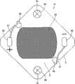
图5是示意性地表示本发明的第一方面发光装置作为本发明的第二方面发光装置实现的情况下优选的第三实施例的发光装置16的俯视图。Fig. 5 is a plan view schematically showing a
图6是示意性地表示本发明的第一方面发光装置作为本发明的第二方面发光装置实现的情况下优选的第四实施例的发光装置31的俯视图。Fig. 6 is a plan view schematically showing a
图7是图6中所表示的例子的发光装置31的剖面图。FIG. 7 is a cross-sectional view of the
图8是示意性地表示本发明的第一方面发光装置作为本发明的第三方面发光装置实现的情况下的第一实施例的发光装置41的俯视图。Fig. 8 is a plan view schematically showing a light-emitting
图9是图8中所表示的例子的发光装置41的剖面图。FIG. 9 is a cross-sectional view of the
图10是示意性地表示本发明的第一方面发光装置作为本发明的第三方面发光装置实现的情况下的第二实施例的发光装置51的俯视图。Fig. 10 is a plan view schematically showing a light emitting device 51 of a second embodiment in the case where the light emitting device of the first aspect of the present invention is realized as the light emitting device of the third aspect of the present invention.
图11是图10中所表示的例子的发光装置51的剖面图。FIG. 11 is a cross-sectional view of the light emitting device 51 of the example shown in FIG. 10 .
图12是示意性地表示本发明的第一方面发光装置作为本发明的第三方面发光装置实现的情况下优选的第三实施例的发光装置56的俯视图。Fig. 12 is a plan view schematically showing a
图13是示意性地表示本发明的第一方面发光装置作为本发明的第三方面发光装置实现的情况下的第四实施例的发光装置61的俯视图。Fig. 13 is a plan view schematically showing a
图14是图13中所表示的例子的发光装置61的剖面图。FIG. 14 is a cross-sectional view of the
图15是示意性地表示本发明的第一方面发光装置作为本发明的第二方面发光装置实现的情况下优选的第五实施例的发光装置66的俯视图。Fig. 15 is a plan view schematically showing a light-
图16是示意性地表示本发明的第一方面发光装置作为本发明的第三方面发光装置实现的情况下优选的第五实施例的发光装置68的俯视图。Fig. 16 is a plan view schematically showing a
图17是示意性地表示本发明的第一方面发光装置作为本发明的第二方面发光装置实现的情况下优选的第六实施例的发光装置78的俯视图。Fig. 17 is a plan view schematically showing a light emitting device 78 according to a sixth preferred embodiment in the case where the light emitting device of the first aspect of the present invention is realized as the light emitting device of the second aspect of the present invention.
图18是示意性地表示本发明的第一方面发光装置作为本发明的第三方面发光装置实现的情况下优选的第六实施例的发光装置80的俯视图。Fig. 18 is a plan view schematically showing a light emitting device 80 according to a sixth preferred embodiment in the case where the light emitting device of the first aspect of the present invention is realized as the light emitting device of the third aspect of the present invention.
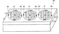
图19是表示图5中所表示的例子的发光装置16适用于荧光灯型LED灯101情况下的立体图。FIG. 19 is a perspective view showing a case where the
图20是表示图17中所表示的例子的发光装置78适用于荧光灯型LED灯111情况下的立体图。FIG. 20 is a perspective view showing a case where the light emitting device 78 of the example shown in FIG. 17 is applied to a fluorescent lamp type LED lamp 111 .
图21是图3中所表示的例子的发光装置11适用于电灯泡型LED灯121情况下的横截面图。FIG. 21 is a cross-sectional view in a case where the
图22是本发明的发光装置适用于荧光灯型LED灯131情况下的立体图。FIG. 22 is a perspective view of a case where the light emitting device of the present invention is applied to a fluorescent lamp
图23是制造图1和2中所表示的例子的发光装置1的情况下本发明发光装置的制造方法的阶段性视图。FIG. 23 is a stepwise view of a method of manufacturing a light emitting device of the present invention in the case of manufacturing the
图24是制造图1和2中所表示的例子的发光装置1的情况下本发明发光装置的制造方法的阶段性视图。FIG. 24 is a stepwise view of a method of manufacturing a light emitting device of the present invention in the case of manufacturing the
图25是制造图8和9中所表示的例子的发光装置41的情况下本发明发光装置的制造方法的阶段性视图。FIG. 25 is a stepwise view of a method of manufacturing a light emitting device of the present invention in the case of manufacturing the
图26是制造图8和9中所表示的例子的发光装置41的情况下本发明发光装置的制造方法的阶段性视图。FIG. 26 is a stepwise view of a method of manufacturing a light emitting device of the present invention in the case of manufacturing the
图27是表示CIE的色度坐标的曲线图。Fig. 27 is a graph showing chromaticity coordinates of CIE.
图28是示意性地表示现有技术中发光二极管201的横截面图。FIG. 28 is a cross-sectional view schematically showing a
图29是示意性地表示现有技术中发光装置301的横截面图。FIG. 29 is a cross-sectional view schematically showing a
具体实施方式Detailed ways
本发明的发光装置(第一方面发光装置)特征在于具有基板和发光部,该发光部,具有:多个发光元件,其搭载在基板上、与外部电极电连接;第一密封体层,其覆盖发光元件的方式形成,并含有第一荧光体;以及第二密封体层,其在第一密封体层上形成,并含有第二荧光体。根据具有这种基本构成的本发明发光装置,能够获得抑制色偏差等、且制造容易的效果。作为本发明的这种第一方面发光装置的具体构成实施例,可以列举下述那种第二方面发光装置或第三方面发光装置。而且,在针对第一方面发光装置、第二方面发光装置和第三方面发光装置全体进行叙述的情况下统称为“本发明的发光装置”。The light-emitting device of the present invention (light-emitting device according to the first aspect) is characterized in that it has a substrate and a light-emitting part. The light-emitting part has: a plurality of light-emitting elements mounted on the substrate and electrically connected to external electrodes; It is formed to cover the light-emitting element and contains the first phosphor; and the second sealing body layer is formed on the first sealing body layer and contains the second phosphor. According to the light-emitting device of the present invention having such a basic configuration, it is possible to obtain effects such as suppression of color shift and ease of manufacture. Specific configuration examples of the light-emitting device of the first aspect of the present invention include the following second-aspect light-emitting device or third-aspect light-emitting device. In addition, when describing the light-emitting device of the first aspect, the light-emitting device of the second aspect, and the light-emitting device of the third aspect, they are collectively referred to as "the light-emitting device of the present invention".
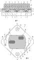
在此,图1是示意性地表示本发明的第一方面发光装置作为本发明的第二方面发光装置实现的情况下优选的第一实施例的发光装置1的俯视图,图2是图1中所表示的例子的发光装置1的剖面图。本发明的第二方面发光装置的特征在于在上述第一方面发光装置的基本构成中,基板是金属基板,在该金属基板表面上形成布线图案,并且形成具有在厚度方向上贯通的多个贯通孔的绝缘基材,发光元件搭载在绝缘基材的贯通孔内的金属基板上,并且与布线图案电连接。在图1和2中表示的本发明的第二方面发光装置1基本具有金属基板2、在金属基板2上形成的绝缘基材3、发光元件4、含有第一荧光体的第一密封体层5以及含有第二荧光体的第二密封体层6。在本发明的第二方面发光装置中,绝缘基材在其表面上形成布线图案7,而且在厚度方向上贯通形成多个贯通孔8。另外,图1和2中表示的本发明的第二方面发光装置1中,在绝缘基材3的贯通孔8内露出的金属基板2上搭载在上表面具有两个电极(未表示)的发光元件4,使用接合线W与布线图案7电连接,由此与外部电极电连接。这样搭载的多个发光元件4被各接合线W覆盖并且由含有第一荧光体的第一密封体层5所密封。另外在该第一密封体层5上形成含有第二荧光体的第二密封体层6。此外,如图2中所示,在形成了布线图案7的绝缘基材3中没有被第一密封体层5覆盖的区域中形成阻焊剂9。Here, FIG. 1 is a top view schematically showing the light-emitting
在本发明的第二方面发光装置1中,多个发光元件4的配置方法不做特别限定,优选一列地配置搭载。而且,在如图1和2中所示的本发明的第二方面发光装置1的情况下,因为可以实现为在一个贯通孔8内一列地配置搭载多个发光元件4,在绝缘基材3的表面上以与该直线状配置平行的方式形成直线状布线图案7,所以在贯通孔8内可以适当调整发光元件4的间隔,并且能够根据所希望的发光亮度(輝度)调整发光元件4的搭载个数,因此是优选的。In the light-emitting
此外在本发明的第二方面发光装置1中,优选以形成相互平行的多个列的方式配置搭载多个发光元件4。通过配置形成这种平行的多个列,可以实现面板状发光装置。而且,该情况下,更优选实现为配置搭载形成相互平行的多个列的发光元件4通过在邻接的列之间共通接线的接合线与布线图案7电连接。In addition, in the light-emitting
在本发明的发光装置中,第一密封体层优选含有第一荧光体并且可以形成为覆盖发光元件。例如,图1和2中表示通过一个第一密封体层5覆盖所有发光元件4而实现的例子。通过如此按照用一个第一密封体层5覆盖所有发光元件4的方式形成,具有能够降低发光装置的亮度不均(ムラ),并且降低第一密封体层的厚度偏差这样的优点。In the light-emitting device of the present invention, the first sealing body layer preferably contains the first phosphor and may be formed to cover the light-emitting element. For example, FIGS. 1 and 2 show an example realized by covering all light-emitting
在此,图3是示意性地表示本发明的第一方面发光装置作为本发明的第二方面发光装置实现的情况下优选的第二实施例的发光装置11的俯视图,图4是图3中所表示的例子的发光装置11的剖面图。图3和4所表示的例子的发光装置11,除了一部分之外,其他与图1和2中所表示的例子的发光装置1相同,对具有相同构成的部分采用相同的附图标记并且省略说明。在本发明的发光装置中,也可以按照用一个第一密封体层覆盖多个发光元件的方式形成第一密封体层。在图3和4中表示如上述那样以形成相互平行的多个列的方式在金属基板12上搭载发光元件4(更优选,以形成相互平行的多个列的方式而配置搭载的发光元件4在邻接的列之间通过共通接线的接合线与布线图案电连接),并且以每列地覆盖所搭载的发光元件4的方式,形成第一密封体层13而成的例子。由此,用一个第一密封体层13按每列对以形成相互平行的多个列的方式而配置搭载的发光元件4,进行覆盖,因而具有能够提高直线状配置的发光元件4的发光亮度,并且强调直线状发光这样的优点。Here, FIG. 3 is a top view schematically showing the light-emitting
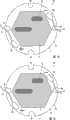
另外图5是示意性地表示本发明的第一方面发光装置作为本发明的第二方面发光装置实现的情况下优选的第三实施例的发光装置16的俯视图。而且,图5中所表示的例子的发光装置16除了一部分之外,其他与图1和3中分别所表示的例子的发光装置1,11相同,对具有相同构成的部分采用相同的附图标记并且省略说明。另外,在图5中示出了以每一个地覆盖发光元件4的方式而多个地形成第一密封体层21的例子。在如此以每一个地覆盖发光元件4的方式而形成第一密封体层21的情况下,具有提高每个发光元件4的发光亮度,并且强调点状发光的优点。5 is a plan view schematically showing a
在本发明的第二方面发光装置中,优选为,以覆盖第一密封体层的至少一部分的方式形成第二密封体层。图1和2中,示出了以覆盖第一密封体层5上的一部分区域的方式形成第二密封体层6的例子。另外在图3和4中表示了如下例子,其中以如对多个第一密封体层13中的一部分的第一密封体13进行覆盖的方式形成第二密封体层13,所述多个第一密封体层13形成为按列对如上述那样以形成相互平行的多个列的方式配置而搭载的发光元件4进行覆盖。另外,图5中示出了如下例子:即以仅对多个第一密封体层21中一部分第一密封体层21进行覆盖的方式多个地形成第二密封体层22,所述多个第一密封体层以每一个地覆盖发光元件4的方式形成。通过如此以部分地形成覆盖第一密封体层5,13,21的方式形成第二密封体层6,14,22,具有可以获得具有所希望的色度特性(例如,落入表示后述的色度坐标的图27(b)的范围内)的发光装置的优点。而且,这种情况下,可以根据所希望的色度特性(例如,没有落入到表示后述的色度坐标的图27(b)的范围内的部分等)选择第一密封体层5,13,21的被第二密封体层6,14,22覆盖的部分。另外,在以部分地覆盖第一密封体层5,13,21的方式形成第二密封体层6,14,22的情况下,第二密封体层当然也可以形成为多个(图1和2所示的例子中为2个,图5中所示的例子中为5个)。而且,在含有第一荧光体的第一密封体层和含有第二荧光体的第二密封体层的边界,可以明确分开,也可以不明确的分开。In the light-emitting device according to the second aspect of the present invention, it is preferable that the second sealing layer is formed to cover at least a part of the first sealing layer. In FIGS. 1 and 2 , an example in which the second
在此,图6是示意性地表示本发明的第一方面发光装置作为本发明的第二方面发光装置实现的情况下的第四实施例的发光装置31的俯视图,图7是图6中所表示的例子的发光装置31的剖面图。而且,图6和7所示的例子的发光装置31除了一部分之外,其他与图1和2中分别所表示的例子的发光装置1相同,对具有相同构成的部分采用相同的附图标记并且省略说明。图6和7所示的例子的发光装置31中,虽然一个第一密封体层5形成为覆盖全部发光元件4这方面与图1和2中所表示的例子的相同,但是以覆盖该第一密封体层5的上表面整个表面的方式形成了第二密封体层32。如此具有如下优点:即由于以覆盖第一密封体层5的全部的方式形成第二密封体层32,因此能够实现这样一种发光装置31,其能够关于第一密封体层5的上表面的全部,以进入下述的图27中表示的色度坐标中(b)范围中的方式,调整色度。Here, FIG. 6 is a top view schematically showing the
接着,对作为本发明的第一方面发光装置中的令一个具体构成实施例的第三方面发光装置进行说明。图8是示意性地表示本发明的第一方面发光装置作为本发明的第三方面发光装置实现的情况下的第一实施例的发光装置41的俯视图,图9是图8中所表示的例子的发光装置41的剖面图。本发明的第三发光装置的特征在于,在上述本发明的第一方面发光装置的基本构成中,基板是金属基板,在该金属基板上形成绝缘基材,并且以在绝缘基材上形成间隔部的方式载置金属板,发光元件与金属板电连接,并且也与隔着间隔部而相邻的金属板电连接。图8和9中表示的本发明的第三方面发光装置41,基本上具有在金属极板42上形成的绝缘基材43、在绝缘基材43上以形成间隔部45的方式载置的金属板44、在金属板44上载置的多个发光元件46、含有第一荧光体的第一密封体层47和含有第二荧光体的第二密封体层48。如图9中所示,本发明的第三方面发光装置41中,发光元件46,也电连接在与搭载该发光元件46的金属板44相邻接的金属板44上。而且,如图8和9中所示的本发明的第三方面发光装置41中,作为发光元件46,使用在上表面具有两个电极(未图示)的发光元件,利用接合线W分别将各电极与金属板44电连接,由此与外部电极电连接。在图9所示的例子中,可以在金属板44上除了搭载发光元件46的区域之外的任何区域上设计阻焊剂49。另外,本发明的第三方面发光装置41中,如图9中表示的例子那样,优选为,在金属板44上形成金属镀层50,在该金属镀层50上搭载发光元件46,发光元件46通过该金属镀层50,与搭载了上述发光元件46的金属板44以及和搭载了该发光元件46的金属板44隔着间隔部45而邻接的金属板44,相电连接。Next, a description will be given of a third light-emitting device as a concrete embodiment of the first light-emitting device of the present invention. Fig. 8 is a top view schematically showing the
本发明的第三方面发光装置41中涉及的多个发光元件46的配置方法不作特别限定,与上述第二方面发光装置一样,优选为,配置搭载成一列。另外,在如图8和9所示那样的本发明的第三方面发光装置41的情况下,优选为,将多个发光元件46配置搭载成一列,并且以形成与该发光元件46的列相平行的间隔部45的方式搭载金属板44。通过如此而实现,具有如下优点:即金属板44以及间隔部45的配置成为搭载发光元件时的标准(目安),并容易将发光元件配置成直线状。进一步地,本发明的第三方面发光装置41与上述第二方面发光装置的情况相同,也优选为,以多个发光元件46形成相互平行的多列的方式而配置搭载。The arrangement method of the plurality of light-emitting
在图8和9中,与图1和2中表示的例子的发光装置1一样,示出了按照用一个第1密封体层47覆盖所有的发光元件46的方式而实现的例子。这样即使在第三方面的发光装置41中,也会因为所有发光元件46被一个密封体层47覆盖而同样获得上述效果。In FIGS. 8 and 9 , an example realized by covering all the
另外图10是示意性地表示本发明的第一方面的发光装置作为本发明的第三方面发光装置而实现的情况下的第二实施例的发光装置51的俯视图,图11是图10中所表示的例子的发光装置51的剖面图。而且,图10和11中所示的例子的发光装置51中除了一部分之外,其他与图8和9中分别所表示的例子的发光装置41相同,对具有相同构成的部分采用相同的附图标记并且省略说明。图11中示出了如下例子:即在金属板44上以形成相互平行的多个列的方式通过金属镀层50搭载发光元件46,并以按每一列覆盖所搭载的发光元件46的方式而形成第一密封体层53。如此,即使在第三方面发光装置51的情况下,若以形成相互平行的多个列的方式而配置搭载发光元件46,并用一个第一密封体层53按每列覆盖如此配置搭载的发光元件46,则也能够获得与第二方面发光装置中同样实现的情况下相同的效果。In addition, FIG. 10 is a top view schematically showing the light emitting device 51 of the second embodiment when the light emitting device of the first aspect of the present invention is realized as the light emitting device of the third aspect of the present invention, and FIG. 11 is a top view of the light emitting device shown in FIG. A cross-sectional view of the light emitting device 51 of the example shown. 10 and 11, the light emitting device 51 of the example shown in FIGS. 10 and 11 is the same as the
另外,图12是示意性地表示本发明的第一方面发光装置作为本发明的第三方面发光装置实现的情况下优选的第三实施例的发光装置56的俯视图。而且,图12中所表示的例子的发光装置56除了一部分之外,其他与图5所示的例子的发光装置16相同,对具有相同构成的部分采用相同的附图标记并且省略说明。即使在本发明的第三方面发光装置的情况,如图12所示,当然也能够以覆盖每个发光元件的方式形成第一密封体层21。在该情况下,对于图5中所表示的例子的发光装置16而言,与上述一样,具有提高各个发给元件4的发光亮度,强调点状发光这样的优点。12 is a plan view schematically showing a
另外图13是示意性地表示本发明的第一方面发光装置作为本发明的第三方面发光装置实现的情况下的第四实施例的发光装置61的俯视图,图14是图13中所表示的例子的发光装置61的剖面图。而且,图13和14中所表示的例子的发光装置61除了一部分之外,其他与图8和9所示的发光装置41相同,对具有相同构成的部分采用相同的附图标记并且省略说明。图13和14中所示的例子的发光装置61虽然在以覆盖所有的发光元件46的方式形成一个第1密封体层47这一方面与图9中表示的例子相同,但是还以覆盖该第一密封体层47的上表面全面的方式形成第二密封体层62。这样一来,如果如图13和14那样以第三方面的发光装置与图6和7中所示的第二方面发光装置31相同的构成,也可以获得与上述相同的效果。In addition, FIG. 13 is a top view schematically showing the light-emitting
本发明的发光装置中,第一密封体层的形状不作特别限定,但是优选具有方形、六边形、圆形或者多个直线状的剖面形状。在此,第一密封体层的剖面形状是指与第一密封体层的金属基板平行的平面的剖面形状。在上述图1,6,8和13中所示的例子的发光装置1,31,41,61中,第一密封体层5,47具有方形剖面形状的情况下,在如此以具有方形剖面形状的方式形成第一密封体5,47的情况下,具有能够确保形成后述固定用孔、外部配线用孔等区域的优点。另外,在下述图3和10中所表示的例子的发光装置11,51中,对于第一密封体层13,53具有多个直线状剖面形状的情况,在如此以具有直线状的剖面形状的方式形成第一密封体13,53的情况下,具有能够提高直线状配置的发光元件亮度,强调直线状发光的优点。In the light-emitting device of the present invention, the shape of the first sealing body layer is not particularly limited, but preferably has a cross-sectional shape of a square, hexagon, circle, or a plurality of straight lines. Here, the cross-sectional shape of the first sealing body layer refers to the cross-sectional shape of a plane parallel to the metal substrate of the first sealing body layer. In the light-emitting
另外,图15是示意性地表示本发明的第一方面发光装置作为本发明的第二方面发光装置实现的情况下优选的第五实施例的发光装置66的俯视图,图16是示意性地表示本发明的第一方面发光装置作为本发明的第三方面发光装置实现的情况下优选的第五实施例的发光装置68的俯视图。而且,图15和16中分别所表示的例子的发光装置66,68除了一部分之外,其他与图3和10分别的例子的发光装置11,51相同,对具有相同构成的部分采用相同的附图标记并且省略说明。在图15和16中示出了如下情况下的发光装置66,68:即按照用一个第一密封体层71覆盖发光元件(未表示)全部的方式形成剖面形状为六边形形状的第一密封体层71,并以部分覆盖该第一密封体层71的方式形成第二密封体层72。而且,在如图15和16所示的例子那样以具有六边形状的剖面形状的方式形成第一密封体层71的情况下,具有因为对称形状而光指向性良好的优点。In addition, FIG. 15 is a top view schematically showing the
图17是示意性地表示本发明的第一方面发光装置作为本发明的第二方面发光装置实现的情况下优选的第六实施例的发光装置78的俯视图,图18是示意性地表示本发明的第一方面发光装置作为本发明的第三方面发光装置实现的情况下优选的第六实施例的发光装置80的俯视图。而且,图17和18中分别表示的例子的发光装置78,80除了一部分之外,其他与图3和10所分别表示的例子的发光装置11,51相同,对具有相同构成的部分采用相同的附图标记并且省略说明。图17和18中,分别示出了如下情况下的发光装置78,80:即按照用一个第一密封体层覆盖发光元件(未图示)全部的方式,形成剖面形状为圆形的第一密封体层76,并以部分覆盖该第一密封体层76的方式形成第二密封体层77。另外,上述图5和12中所表示的例子的发光装置16,56,是以按每个对发光元件进行覆盖的方式形成的第一密封体层21具有圆形状的剖面形状的情况。根据图5,12,17和18中分别表示的实施例那样,在以具有圆形状的剖面形状的方式形成第一密封体层21,76的情况下,具有因为对称形状而光指向性良好的优点。Fig. 17 is a top view schematically showing the light emitting device 78 of the sixth embodiment when the light emitting device of the first aspect of the present invention is realized as the light emitting device of the second aspect of the present invention, and Fig. 18 schematically shows the light emitting device of the present invention A top view of the light emitting device 80 of the sixth embodiment when the light emitting device of the first aspect of the present invention is realized as the light emitting device of the third aspect of the present invention. Moreover, the light emitting devices 78 and 80 of the examples shown respectively in FIGS. 17 and 18 are the same as the
另外,本发明的发光装置中的第一密封体层以及/或者第二密封体层,也可以,形成为成为向上方凸起的半球状。该情况下,第一密封体以及/或者第二密封体中可以具有作为透镜的功能。In addition, the first sealing body layer and/or the second sealing body layer in the light-emitting device of the present invention may be formed in a hemispherical shape convex upward. In this case, the first sealing body and/or the second sealing body may function as a lens.
本发明的发光装置对其整体形状不作特别限制,但是优选实现为具有六边形、圆形、长方形或者正方形的剖面形状。在此,发光装置的剖面形状是指与基板的基板面平行的平面的剖面形状。在发光装置具有长方形或者正方形的剖面形状的情况下,因为能够使发光元件紧贴(密着)配置,所以发光装置在适用于荧光灯型LED灯的情况下是特别优选的。另外,在发光装置适用于电灯泡型LED灯(下述)的情况下,发光装置优选以具有圆形剖面形状的方式实现。另外,在辉点(輝点)发光成为问题的情况下,发光装置优选实现为具有六边形、长方形或者正方形的剖面形状。图1,6,8和13中示处了以具有正方形剖面形状的方式实现的发光装置1,31,41,61。另外,图3,5,10,12,15,16,17,18中,示出了以具有圆形剖面形状的方式实现的发光装置11,16,51,56,66,68,78,80。The light emitting device of the present invention is not particularly limited in its overall shape, but is preferably realized to have a hexagonal, circular, rectangular or square cross-sectional shape. Here, the cross-sectional shape of the light-emitting device refers to the cross-sectional shape of a plane parallel to the substrate surface of the substrate. When the light-emitting device has a rectangular or square cross-sectional shape, since the light-emitting elements can be arranged in close contact (close contact), the light-emitting device is particularly preferable when applied to a fluorescent lamp type LED lamp. In addition, when the light emitting device is applied to a light bulb type LED lamp (described below), it is preferable that the light emitting device is realized to have a circular cross-sectional shape. In addition, in the case where bright-spot (bright-spot) light emission is a problem, the light-emitting device is preferably realized to have a hexagonal, rectangular, or square cross-sectional shape. In FIGS. 1 , 6 , 8 and 13 there are shown light emitting
因为本发明的发光装置能够抑制色偏差等,同时容易制造,所以特别适于用作液晶显示器的背光光源或者照明用光源。通过使用本发明的发光装置,可以实现包含白色的电灯泡色等任意色调的上述光源。Since the light-emitting device of the present invention can suppress color shift and the like and is easy to manufacture, it is particularly suitable for use as a backlight light source for a liquid crystal display or as a light source for illumination. By using the light-emitting device of the present invention, it is possible to realize the above-mentioned light source of any color such as light bulb color including white.
本发明的发光装置为了提供上述用途,通常具有用于安装、固定在对方部件上的固定用孔。在图1,6,8和13所示的具有正方形剖面的发光装置1,31,41,61中,示出了如下情况:即在具有正方形剖面形状的金属基板2,42的相面对的角部,形成一个固定用孔81,该固定用孔81以贯通金属基板2,42的方式设置,并在对角线上各备置一个。另外,图3,5,10,12,15,16,17,18中所示的具有圆形剖面形状的发光装置11,16,51,56,66,68,78,80中,示出了如下例子:切口状固定用孔82,在通过具有圆形剖面形状的金属基板12,52的中心的直线上各配置一个。另外,如图5和12中所示的例子的发光装置16,56中那样,在以按每一个对发光元件进行覆盖而形成第一密封体层21和第二密封体层22情况下,在剖面为圆形的金属基板12,52的中心附近的区域上没有搭载发光元件,在该中心附近的区域上设计位置对准(合わせ)用孔83。In order to provide the above-mentioned application, the light-emitting device of the present invention usually has a fixing hole for mounting and fixing to a counterpart member. In the light-emitting
另外、为了提供上述用途,可以使用固定用工具将本发明的发光装置安装、固定在对方部件上。作为该固定用工具,例如如图1,6,8和13中的固定用工具(冶具)84那样,可以列举出:在内壁上形成有螺纹牙(ネジ)、并且能够插入、螺纹连接(螺合)在固定用孔81中的螺丝等。另外固定用工具可以是粘接片等。In addition, in order to provide the above-mentioned application, the light-emitting device of the present invention can be mounted and fixed on a counterpart member using a fixing tool. As the fixing tool, for example, like the fixing tool (jig) 84 in FIGS. together) screws or the like in the fixing holes 81. In addition, the fixing tool may be an adhesive sheet or the like.
在此,图19到22中,分别表示本发明的发光装置适用作照明光源的例子。图19是表示将图5所表示的例子的发光装置16适用于荧光灯型LED灯101情况下的立体图,图20是表示将图17中所表示的例子的发光装置78适用于荧光灯型LED灯111情况下的立体图,图21是图3中所表示的例子的发光装置11适用于电灯泡型LED灯121情况下的立体图。如图19到21中所示,分别使用固定用工具84在固定用孔82中安装固定发光装置16,78,11。另外图22是本发明的发光装置适用于荧光灯型LED灯131情况下的立体图,如图22所示,可以将对方部件的安装面132作为金属基板而使用,从而直接搭载发光元件,由第一密封体层133和第二密封体层134密封。Here, FIGS. 19 to 22 show examples in which the light-emitting device of the present invention is applied as an illumination light source, respectively. 19 is a perspective view showing the case where the light-emitting
另外,本发明的发光装置,分别如图1,3,5,6,8,10,12,13,15,16,17和18所示,在金属基板2,12,42,52上,作为外部电极设置正电极外部连接区域85和负电极外部连接区域86,并优选设置外部连接配线87,所述连接配线87用于对该正电极外部连接区域85以及负电极外部连接区域86与电源(未图示)之间分别进行电连接。发光元件电连接在该正电极外部连接区域85和负电极外部连接区域86。In addition, the light-emitting device of the present invention, as shown in Figures 1, 3, 5, 6, 8, 10, 12, 13, 15, 16, 17 and 18, is on the
另外本发明的发光装置分别如图1,3,5,6,8,10,12,13,15,16,17和18中所示,优选在金属基板2,12,42,52上形成用于通过外部连接配线87的外部配线用孔88。图1,6,8和13中表示的实施例中,在具有正方形剖面形状的金属基板2,42上,以配置在与设置有上述的固定用孔81的对角线不同的另一对角线上的方式,设置正电极外部连接区域85和负电极外部连接区域86,进一步地在金属基板2,42的相面对的两个边的中央附近形成切口状外部配线用孔88。另外,在图3,5,10,12,15,16,17和18中表示的实施例中,在具有圆形剖面形状的金属基板12,52上,在与如上述那样形成有固定用孔82且通过中心的直线大致相垂直并通过中心的直线上,形成切口状外部配线用孔88,在该固定用孔82和外部配线用孔88之间相面对地设计正电极外部连接区域85和负电极外部连接区域86。而且,如图3,5,10,12,15,16,17和18中表示的例子那样,对于在具有圆形剖面形状的金属基板12,52上以切口状形成固定用孔82和外部配线用孔88的情况,在被安装在对方部件上的状态下,能够起到防止发光装置在圆周方向上转动而阻止旋转的效果。In addition, the light-emitting device of the present invention is shown in Figures 1, 3, 5, 6, 8, 10, 12, 13, 15, 16, 17 and 18 respectively, and is preferably formed on a
作为本发明的发光装置中使用的发光元件,不特别限制使用本领域中通常使用的发光元件。作为这种发光元件,例如可以列举,在蓝宝石(サファイヤ)基板、ZnO(氧化锌)基板、GaN基板、Si基板、SiC基板、尖晶石(スピネル)等基板上生长氮化镓(ガリウム)系化合物半导体、ZnO(氧化锌)系化合物半导体、InGaAlP系化合物半导体、AlGaAs系化合物半导体等材料的蓝色系LED(发光二极管)芯片等半导体发光元件。其中,由于容易在绝缘性基板上制作片面2电极构造,并且能够产量性良好地形成结晶性好的氮化物半导体,所以优选使用在蓝宝石基板上生长氮化镓系化合物半导体的蓝色系LED作为发光元件。在使用这种蓝色系LED作为发光元件的情况下,优选由该半导体发光元件发出的光激发并且在密封体中分散有发出黄色系光的荧光体,从而实现能够获得白色的发光装置(下述)。而且,在本发明的发光装置中使用的发光元件的发光色不局限于蓝色发光,当然也可以使用例如紫外线发光、绿色发光等发光色的发光元件。As the light-emitting element used in the light-emitting device of the present invention, light-emitting elements generally used in this field are not particularly limited. Examples of such light-emitting devices include gallium nitride-based substrates grown on substrates such as sapphire substrates, ZnO (zinc oxide) substrates, GaN substrates, Si substrates, SiC substrates, and spinels. Semiconductor light-emitting elements such as blue LED (light-emitting diode) chips made of compound semiconductors, ZnO (zinc oxide)-based compound semiconductors, InGaAlP-based compound semiconductors, and AlGaAs-based compound semiconductors. Among them, since it is easy to form a one-sided two-electrode structure on an insulating substrate, and a nitride semiconductor with good crystallinity can be formed with good productivity, it is preferable to use a blue LED in which a gallium nitride-based compound semiconductor is grown on a sapphire substrate. light emitting element. When such a blue LED is used as a light-emitting element, it is preferable to excite the light emitted by the semiconductor light-emitting element and to disperse a phosphor emitting yellow light in the sealing body, so as to realize a white light-emitting device (below). described). Furthermore, the luminescent color of the light-emitting element used in the light-emitting device of the present invention is not limited to blue luminescence, and it is of course possible to use light-emitting elements with luminescent colors such as ultraviolet light and green light.
另外作为在本发明的发光装置中使用的发光元件,在图2,4,7,9,11和14示出了,使用上表面上具有两个电极的发光元件(即,在一个面上形成P侧电极以及N侧电极,并将该作为上表面而搭载)的情况。该情况下,如图2,4,7,9,11和14中所示,可以使用连接线W而分别连接P侧电极和N侧电极。本发明的发光装置中,当然可以使用上下面上各具有一个电极的发光元件。这种情况下,例如也可以构成为,以一方的电极成为上表面的方式,搭载一面上形成P侧电极而相面对的面上形成N侧电极的发光元件,并且对于配置在上表面侧的电极使用一根连接线电连接。而且,在这种情况下,在形成了发光元件的电极的下面,使用例如AuSn、Ag浆料等具有导电性的粘结剂而进行接合。In addition, as a light-emitting element used in the light-emitting device of the present invention, shown in FIGS. P-side electrode and N-side electrode, and this is mounted as the upper surface). In this case, as shown in FIGS. 2 , 4 , 7 , 9 , 11 , and 14 , the P-side electrode and the N-side electrode may be connected using connection wires W, respectively. In the light-emitting device of the present invention, of course, a light-emitting element having one electrode on each of the upper and lower surfaces can be used. In this case, for example, a light emitting element having a P-side electrode formed on one surface and an N-side electrode formed on the opposite surface may be mounted such that one electrode becomes the upper surface, The electrodes are electrically connected using a connecting wire. Furthermore, in this case, bonding is performed using a conductive adhesive such as AuSn or Ag paste, for example, on the lower surface of the electrode on which the light emitting element is formed.
作为本发明的发光装置中用于发光元件的电连接的连接线W,不特别局限于使用本领域中根据现有技术广泛使用的适合的金属细线。作为这种金属细线,可以列举例如金线、铝线、铜线、铂(白金)线等,但是其中从腐蚀性小、耐湿性、耐环境性、粘着性、导电性、导热性、延伸率良好、容易出孔方面考虑,优选用金线作为连接线W。As the connection wire W used for the electrical connection of the light-emitting element in the light-emitting device of the present invention, it is not particularly limited to use suitable thin metal wires widely used in the art according to the prior art. Such thin metal wires include, for example, gold wires, aluminum wires, copper wires, platinum (platinum) wires, etc., but among them, the corrosion resistance, moisture resistance, environment resistance, adhesion, electrical conductivity, thermal conductivity, elongation, etc. In terms of good efficiency and easy hole exit, gold wires are preferably used as the connecting wires W.
作为构成本发明的发光装置的金属基板、绝缘基材、金属板、金属镀层、第一密封体层、第二密封体层等,分别适当地采用本领域中比现有技术更广泛使用的材料。As the metal substrate, insulating base material, metal plate, metal plating layer, first sealing body layer, second sealing body layer, etc. constituting the light-emitting device of the present invention, materials that are more widely used in this field than the prior art are appropriately used. .
作为金属基板,可以使用由从例如铝、铜、铁等中选出的至少一种金属材料构成的基板,不作特别限制。其中,从导热性良好、光反射率高方面考虑,优选使用铝制金属基板。As the metal substrate, a substrate composed of at least one metal material selected from, for example, aluminum, copper, iron, etc. can be used without particular limitation. Among them, it is preferable to use an aluminum metal substrate from the viewpoint of good thermal conductivity and high light reflectance.
作为绝缘基材,可以使用例如聚酰亚胺(ポリイミド)等具有绝缘性的材料层状形成的基材,不特别限制。而且,作为上述本发明的第二方面发光装置中使用的绝缘基材,可以适当地使用根据所需要的发光形成贯通孔并且在表面上形成适当布线图案(例如由金箔膜、在铜上电镀的铜箔膜等材料形成)的基材。As the insulating base material, for example, a base material formed in a layered form of an insulating material such as polyimide (polyimide) can be used, and it is not particularly limited. Furthermore, as the insulating base material used in the light-emitting device of the second aspect of the present invention described above, it is possible to suitably use a material with through holes formed according to the required light emission and an appropriate wiring pattern formed on the surface (for example, a gold foil film, copper plated Copper foil film and other materials) base material.
在上述本发明的第三方面发光装置中,以在绝缘基材上形成间隔部的方式搭载金属板,其中作为金属板可以使用由例如铜等金属形成的板状物,不作特别限制。另外,本发明第三方面的发光装置中,作为金属板上形成的金属镀层,可以列举使用银、金等金属的镀层,但是不作特别限制。其中,从光反射率高方面考虑,优选使用银镀层。形成金属镀层时,通过在金属板上搭载具有与所需要的布线图案相对应形状的掩膜的状态下形成金属镀层,而以具有所需要布线图案的方式在金属板上形成金属镀层。In the light-emitting device according to the third aspect of the present invention, the metal plate is mounted on the insulating base material so as to form a spacer. The metal plate can be a plate-shaped object made of metal such as copper, and is not particularly limited. In addition, in the light-emitting device according to the third aspect of the present invention, examples of the metal plating layer formed on the metal plate include plating layers using metals such as silver and gold, but are not particularly limited. Among them, silver plating is preferably used from the viewpoint of high light reflectance. When forming the metal plating layer, the metal plating layer is formed on the metal plate so as to have the desired wiring pattern by placing a mask having a shape corresponding to the desired wiring pattern on the metal plate.
作为用于形成本发明发光装置中的第一密封体层和第二密封体层的材料(密封材料),是具有透光性的材料即可,不作特别限制,可以使用本领域中根据现有技术广泛使用的材料。作为这种密封材料,合适使用例如环氧树脂、尿素(エリア)树脂、硅酮(シリコ一ン)树脂等耐气候性优异的透光性树脂、耐光性优异的硅溶胶(シリカゾル)、玻璃(硝子)等透光性无机材料。As the material (sealing material) used to form the first sealing body layer and the second sealing body layer in the light-emitting device of the present invention, it is only necessary to have a light-transmitting material, and it is not particularly limited. Materials widely used in technology. As such a sealing material, for example, light-transmitting resins excellent in weather resistance such as epoxy resins, urea resins, and silicone resins, silica sol (silica sol) excellent in light resistance, glass ( Glass) and other light-transmitting inorganic materials.
作为本发明的发光装置中使用的荧光体(第一密封体层中使用的第一荧光体和第二密封体层中使用的第二荧光体),适合使用例如Ce:YAG(铈活化钇·铝·镓:セリウム赋活イツトリウム·アルミニウム·ガネツト)荧光体、Eu:BOSE(铕活化钡·锶·邻硅酸盐ユ一ロピウム赋活バリウム·オルソシリケ一ト)、Eu:SOSE(铕活化锶·钡·邻硅酸盐:ユ一ロピウム赋活ストロンチウム·バリウム·オルソシリケ一ト)、铕活化硫代长(ユ一ロピウム赋活αサイアロン)荧光体等,但是不局限于此。As the phosphor used in the light-emitting device of the present invention (the first phosphor used in the first sealing body layer and the second phosphor used in the second sealing body layer), for example, Ce:YAG (cerium-activated yttrium. Aluminum Gallium: Cellium Activated Itutrium Alminium Ganet) Phosphor, Eu: BOSE (Europium Activated Barium Strontium Orthosilicate Yuropium Activated Barium Orusosiliket), Eu: SOSE (Europium Activated Strontium · Barium o-silicate: ユビロプユョラデウュルストロンチュム Barium オルソゲリケケット), europium-activated thiolong (Uyropium activating αSiyalon) phosphor, etc., but not limited thereto.
此外,本发明中的第一密封体层和第二密封体层中也可以共同含有荧光体和扩散剂。作为扩散剂,不作特别限制,适合使用例如钛酸钡(チタン酸バリウム)、氧化钛(酸化チタン)、氧化铝、氧化硅、碳酸钙、二氧化硅等。In addition, the first sealing body layer and the second sealing body layer in the present invention may also contain a phosphor and a diffusing agent together. The diffusing agent is not particularly limited, and for example, barium titanate (Chitanate barium), titanium oxide (Titanate), alumina, silicon oxide, calcium carbonate, silicon dioxide, and the like are suitably used.
如后所述,为了通过形成第二密封体层而调整只形成了第一密封体层的状态下的发光装置的色度以使得没有发生色度偏差,可以适当选择第二密封体层中使用的密封材料和荧光体的种类、组成。作为适合的具体例子,示出了如下情况:即作为树脂材料使用甲基硅酮树脂(メチルシリコ一ン),在其中作为第一荧光体而分散Eu:BOSE,并以覆盖该第一密封体层的方式,作为树脂材料使用有机变性的硅酮,在其中作为第二荧光体分散Eu:BOSE,并通过硬化而形成第二密封体层。As will be described later, in order to adjust the chromaticity of the light-emitting device in the state where only the first sealing material layer is formed by forming the second sealing material layer so that no chromaticity deviation occurs, the second sealing material layer can be appropriately selected. The type and composition of sealing materials and phosphors. As a suitable specific example, the following case is shown: that is, a methyl silicone resin is used as the resin material, Eu:BOSE is dispersed therein as the first phosphor, and the first sealing body layer is covered with In this method, organically modified silicone is used as the resin material, Eu:BOSE is dispersed as the second phosphor in it, and the second sealing layer is formed by curing.
另外,在本发明中,对发光装置的制造方法不作特别限制。在上述本发明的发光装置中,对其制造方法不作特别限制,但是可以通过适于本发明发光装置的制造方法进行适当制造。上述本发明的第一方面发光装置可以通过包含下述步骤的方法适当地制造,其中包括:在基板上搭载多个发光元件,将发光元件与外部电极电连接的工序(发光元件搭载工序);以覆盖发光元件的方式形成含有第一荧光体的第一密封体层的工序(第一密封体层形成工序);测定第一密封体层形成之后发光装置的色度特性的工序(色度测定工序);以能够根据所测定的色度特性调整色度偏差的方式在第一密封体层上形成第二密封体层的工序(第二密封体层形成工序)。In addition, in the present invention, the manufacturing method of the light emitting device is not particularly limited. In the light-emitting device of the present invention described above, the manufacturing method thereof is not particularly limited, but can be appropriately manufactured by a manufacturing method suitable for the light-emitting device of the present invention. The above-mentioned light-emitting device according to the first aspect of the present invention can be suitably manufactured by a method comprising: mounting a plurality of light-emitting elements on a substrate, and electrically connecting the light-emitting elements to external electrodes (light-emitting element mounting step); A step of forming a first sealing body layer containing a first phosphor to cover the light-emitting element (first sealing body layer forming step); a step of measuring the chromaticity characteristics of the light-emitting device after the formation of the first sealing body layer (chromaticity measurement step); a step of forming a second sealing body layer on the first sealing body layer so that chromaticity variation can be adjusted based on the measured chromaticity characteristics (second sealing body layer forming step).
首先,在发光元件搭载工序中,在基板上搭载多个发光元件,将发光元件与外部电极电连接。在制造作为本发明的第一方面发光装置的一个具体构成例的第二方面发光装置(例如图1到7,15和17中所示的发光装置1,11,16,31,66,78)的情况下,该发光元件搭载工序中,作为所述基板使用上述的金属板,在该金属板上具有贯通孔,并且形成形成有布线图案的绝缘基材,在贯通孔中搭载发光元件,将外部电极(具体地上述正电极外部连接区域和负电极外部连接区域)与预先电连接的布线图案电连接。First, in the light emitting element mounting step, a plurality of light emitting elements are mounted on a substrate, and the light emitting elements are electrically connected to external electrodes. In manufacturing the second aspect light-emitting device (such as the light-emitting
在此,图23和24是阶段性地表示制造图1和2中所表示的例子的发光装置1的情况下的本发明发光装置的制造方法的图。首先,准备金属基板2(图23(a)),在该金属基板2上形成贯通孔8,并且形成在表面上形成了布线图案7的绝缘基材3(图23(b))。该绝缘基材3的形成可以通过在金属基板2上涂布例如上述的聚酰亚胺(ポリイミド)等具有绝缘性的材料后,干燥而形成。接着,如图23(c)所示那样,在绝缘基材3的贯通孔8内露出的金属基板2上搭载发光元件4,使用连接线W电连接发光元件4和布线图案7。在制造图1和2中所表示的例子的发光装置1的情况下,接着围绕搭载发光元件4的区域在绝缘基材3上形成阻焊剂9,进一步在其上搭载橡胶薄片10(图23(d))。作为橡胶薄片10,适于使用具有贯通孔的硅酮(シリコ一ン)橡胶薄片。根据形成了的第一密封体层的形状(具有上述那样的方形、六边形、圆形、多个直线状等剖面形状的形状等),适当选择该橡胶薄片10的贯通孔的形状。Here, FIGS. 23 and 24 are diagrams showing stepwise a method of manufacturing the light emitting device of the present invention in the case of manufacturing the
另外,制造作为本发明第一方面的发光装置的具体构成例的其一的第三方面发光装置(例如图8到14,16和18中所示的发光装置41,51,56,61,68,80)的情况下,在该发光元件搭载工序中,作为上述基板使用金属板,在该金属板上形成绝缘基材,在绝缘基材上搭载形成间隔部的金属板,在金属板上(通过金属镀层)搭载发光元件,使发光元件与金属板电连接,同时隔着间隔部与相邻的金属板电连接。In addition, a light-emitting device of the third aspect (such as the light-emitting
在此,图25和26是阶段性地表示制造图8和9中所示的例子的发光装置41的情况下本发明发光装置的制造方法的视图。首先,准备金属基板42(图25(a)),在该金属基板42上形成绝缘基材43(图25(b))。该绝缘基材43的形成,如上述关于第二方面发光装置的制造所述,可以通过在金属基板42上涂布聚酰亚胺等具有绝缘性的材料后,干燥而形成。接着,在绝缘基材43上以能够形成间隔部45的方式载置金属板44,并进一步形成金属镀层50。在形成金属镀层50的时候,在金属板44上搭载与所需要的配线的图形相对应的掩膜的状态下形成金属镀层50。接着,在金属镀层50上形成阻焊剂(ソルダ一レジスト)49,在该阻焊剂49上搭载橡胶薄片10(图25(c))。与第二方面发光装置的制造方法中描述的相同,橡胶薄片10适于使用具有适当形状贯通孔的硅酮橡胶薄片。接着,如图26(a)所示,在金属镀层50上除了设计上述阻焊剂49的区域之外的区域上搭载发光元件46。进一步地,使用金线等连接线W,使发光元件46和搭载该发光元件46的金属板44(通过图26(a)中所示的例子中的金属镀层50)电连接,同时隔着间隔部45使发光元件46和与搭载了该发光元件46的金属板44相邻接的金属板44电连接(通过图26(a)所表示的例子中的金属镀层50)。Here, FIGS. 25 and 26 are views showing stepwise the manufacturing method of the light emitting device of the present invention in the case of manufacturing the
在接下来的第一密封体层形成工序中,形成含有第一荧光体的第一密封体层以覆盖发光元件。具体而言,在制造第二方面发光装置、第三方面发光装置中任何一个的情况下,在由阻焊剂9,49和橡胶薄片10包围的搭载发光元件4,46的区域中注入含有第一荧光体的密封材料,并硬化,从而以覆盖发光元件4,46的方式形成第一密封体层5,47(图24(a),图26(b))。在使用由氮化镓系半导体构成的蓝色系半导体发光元件作为上述这种发光元件4,46的情况下,作为第一密封体层5,47中包含的第一荧光体,适合使用由该半导体发光元件发出的光激励而发出黄色系光的荧光体。在形成第一密封体层的时候,将第一荧光体在上述环氧树脂、硅酮树脂等透光性树脂材料等密封材料中进行预分散,可以在滴下而填充到橡胶薄片10的贯通孔内后硬化,也可以采用使用模具而预成型的树脂密封体。而且,作为使密封材料硬化的方式,根据使用的密封材料采用现有技术中公知的适当的方法,不作特别限制。例如作为密封材料的透光性树脂材料使用硅酮树脂的情况下,可以通过使硅酮树脂热硬化来使密封材料硬化。In the subsequent first sealing layer forming step, the first sealing layer containing the first phosphor is formed so as to cover the light emitting element. Specifically, in the case of manufacturing any one of the light-emitting device of the second aspect and the light-emitting device of the third aspect, the first The phosphor sealing material is hardened to form the
在接下来的色度测定工序中,对形成上述第一密封体层形成工序中得到的第一密封体层后的发光装置的色度进行测定。该发光装置的色度特性的测定,例如可以使用采用了以JIS Z 8722的条件C,DIN5033teri7,ISOk772411为基准的d·8(扩散照明8°受光方式)光学系的测定装置进行测定。在此,图27是表示CIE(国际照明委员会)的色度坐标的曲线图。例如,在为了发出CIE的色度表中x,y=(0.325,0.335)的光,而将以5∶100的重量比混合第一荧光体和作为密封材料的硅酮树脂的物质注入到硅酮橡胶薄片10的贯通孔中,在150°的温度下热硬化1小时形成第一密封体层的情况下,形成的第一密封体层的色度变化范围在图27中(a)的区域内。在对具有这种第一密封体层的发光装置测定色度特性的情况下色度范围从犯图27中的(b)的区域偏离。为了调整这种色度偏差,通过接下来的第二密封体层形成工序形成第二密封体层。In the next chromaticity measurement step, the chromaticity of the light-emitting device after forming the first sealing body layer obtained in the first sealing body layer forming step is measured. The measurement of the chromaticity characteristics of the light-emitting device can be performed using, for example, a measurement device using a d.8 (diffuse
在第二密封体层形成工序中,根据上述色度测定工序测定的第一密封体层形成后的发光装置的色度特性,在第一密封体层上形成第二密封体层,从而调整得到的色度偏差。具体而言,对制造第二方面发光装置、第三方面发光装置中任何一种的情况,与上述第一密封体层形成工序相同,在第一密封体层5,47上注入含有第二荧光体的密封材料,并使之硬化,形成第二密封体层6,48(图24(c),图26(c))。In the second sealing body layer forming step, the second sealing body layer is formed on the first sealing body layer based on the chromaticity characteristics of the light-emitting device after the first sealing body layer is formed measured in the above-mentioned chromaticity measuring step, thereby adjusting to obtain color deviation. Specifically, in the case of manufacturing any of the light-emitting device of the second aspect and the light-emitting device of the third aspect, it is the same as the above-mentioned first sealing body layer forming process, and the second fluorescent light is injected into the first
可以根据所需要的色度特性,在用于形成上述第一密封体层的第一荧光体和密封材料中,适当选择用于形成第二密封体层6,48的第二荧光体以及密封材料,并可以根据情况进一步添加使用扩散剂。上述实施例的情况中,在为了得到成为CIE的色度表中x,y=(0.345,0.35)的光而将以5∶100的重量比混合第二荧光体和作为硅酮树脂的密封材料混合物注入到第一密封体层中,在150°的温度下热硬化1小时,而形成第二密封体层。由此,形成第二密封体层后,能够在同样地测定发光装置的色度特性的情况下,得到图27中(b)的区域中的色度范围的发光装置。The second phosphor and sealing material used to form the second
通过在形成第二密封体层之后,除去橡胶薄片10,制造如上述那样的本发明的发光装置。如上所述,在硅酮橡胶薄片10的一面上粘接双面粘接薄片,通过该粘接薄片粘接,可以容易地去除。而且,硅酮橡胶薄片可以多次使用。The light-emitting device of the present invention as described above is produced by removing the
在本发明的发光装置的制造方法中,优选对上述那样形成了第二密封体之后的发光装置测定色度特性。色度特性的测定方法,可以与针对第一密封体层形成后的发光装置进行的上述方法相同。In the method of manufacturing a light-emitting device of the present invention, it is preferable to measure chromaticity characteristics of the light-emitting device after the second sealing body is formed as described above. The measurement method of the chromaticity characteristic may be the same as the above-mentioned method for the light-emitting device after the formation of the first sealing body layer.
虽然表示了本发明的详细说明,但是可以理解这仅仅是用于所表示的例子,不是要局限于此,本发明的范围由附带的权利要求的范围解释。While a detailed description of the present invention has been presented, it is to be understood that this is for the purpose of representing an example only and is not intended to be limiting, and the scope of the present invention is to be interpreted by the scope of the appended claims.
Claims (22)
Translated fromChineseApplications Claiming Priority (3)
| Application Number | Priority Date | Filing Date | Title |
|---|---|---|---|
| JP2007-077313 | 2007-03-23 | ||
| JP2007077313 | 2007-03-23 | ||
| JP2007077313AJP5089212B2 (en) | 2007-03-23 | 2007-03-23 | LIGHT EMITTING DEVICE, LED LAMP USING THE SAME, AND METHOD FOR MANUFACTURING LIGHT EMITTING DEVICE |
Related Child Applications (1)
| Application Number | Title | Priority Date | Filing Date |
|---|---|---|---|
| CN2012100074754ADivisionCN102569280A (en) | 2007-03-23 | 2008-03-21 | Light emitting device and method for manufacturing the same |
Publications (2)
| Publication Number | Publication Date |
|---|---|
| CN101312185Atrue CN101312185A (en) | 2008-11-26 |
| CN101312185B CN101312185B (en) | 2012-02-29 |
Family
ID=39773983
Family Applications (2)
| Application Number | Title | Priority Date | Filing Date |
|---|---|---|---|
| CN2008101314744AActiveCN101312185B (en) | 2007-03-23 | 2008-03-21 | Light emitting device and manufacturing method thereof |
| CN2012100074754APendingCN102569280A (en) | 2007-03-23 | 2008-03-21 | Light emitting device and method for manufacturing the same |
Family Applications After (1)
| Application Number | Title | Priority Date | Filing Date |
|---|---|---|---|
| CN2012100074754APendingCN102569280A (en) | 2007-03-23 | 2008-03-21 | Light emitting device and method for manufacturing the same |
Country Status (3)
| Country | Link |
|---|---|
| US (1) | US7872418B2 (en) |
| JP (1) | JP5089212B2 (en) |
| CN (2) | CN101312185B (en) |
Cited By (12)
| Publication number | Priority date | Publication date | Assignee | Title |
|---|---|---|---|---|
| CN101846256A (en)* | 2010-05-04 | 2010-09-29 | 蔡州 | LED light source |
| CN102155679A (en)* | 2010-01-15 | 2011-08-17 | Lg伊诺特有限公司 | Light emitting module, backlight unit, and display apparatus |
| CN102252181A (en)* | 2011-04-15 | 2011-11-23 | 新高电子材料(中山)有限公司 | A kind of low thermal resistance LED lamp and preparation method thereof |
| CN102483201A (en)* | 2010-07-20 | 2012-05-30 | 松下电器产业株式会社 | Bulb type lamp |
| CN102812571A (en)* | 2010-03-31 | 2012-12-05 | 端点工程有限公司 | Optical device and manufacturing method thereof |
| CN103531584A (en)* | 2012-07-06 | 2014-01-22 | Lg伊诺特有限公司 | Light emitting device package |
| CN103748405A (en)* | 2011-12-16 | 2014-04-23 | 松下电器产业株式会社 | Light-emitting module, light source for lighting and lighting device using the light-emitting module |
| CN104091815A (en)* | 2010-10-12 | 2014-10-08 | 晶元光电股份有限公司 | Light emitting element |
| CN104282829A (en)* | 2009-02-13 | 2015-01-14 | 夏普株式会社 | Light-emitting apparatus and method for manufacturing same |
| US9666558B2 (en) | 2015-06-29 | 2017-05-30 | Point Engineering Co., Ltd. | Substrate for mounting a chip and chip package using the substrate |
| US9847462B2 (en) | 2013-10-29 | 2017-12-19 | Point Engineering Co., Ltd. | Array substrate for mounting chip and method for manufacturing the same |
| CN113491017A (en)* | 2019-02-21 | 2021-10-08 | 电化株式会社 | Phosphor substrate, light-emitting substrate, method for producing phosphor substrate, method for producing light-emitting substrate, and lighting device |
Families Citing this family (75)
| Publication number | Priority date | Publication date | Assignee | Title |
|---|---|---|---|---|
| JP5158472B2 (en) | 2007-05-24 | 2013-03-06 | スタンレー電気株式会社 | Semiconductor light emitting device |
| TW201022576A (en)* | 2008-12-11 | 2010-06-16 | Advanced Connectek Inc | Light emitting diode lamp source module |
| DE102009008738A1 (en)* | 2009-02-12 | 2010-08-19 | Osram Opto Semiconductors Gmbh | Semiconductor device and method for manufacturing a semiconductor device |
| JP5330889B2 (en)* | 2009-04-14 | 2013-10-30 | 電気化学工業株式会社 | LED module for lighting |
| US8337030B2 (en)* | 2009-05-13 | 2012-12-25 | Cree, Inc. | Solid state lighting devices having remote luminescent material-containing element, and lighting methods |
| US8922106B2 (en)* | 2009-06-02 | 2014-12-30 | Bridgelux, Inc. | Light source with optics to produce a spherical emission pattern |
| JP2011009298A (en) | 2009-06-23 | 2011-01-13 | Citizen Electronics Co Ltd | Light-emitting diode light source device |
| JP5354191B2 (en)* | 2009-06-30 | 2013-11-27 | 東芝ライテック株式会社 | Light bulb shaped lamp and lighting equipment |
| JP5379615B2 (en)* | 2009-09-09 | 2013-12-25 | パナソニック株式会社 | Lighting device |
| JP5623062B2 (en) | 2009-11-13 | 2014-11-12 | シャープ株式会社 | Light emitting device and manufacturing method thereof |
| JP2011151268A (en) | 2010-01-22 | 2011-08-04 | Sharp Corp | Light emitting device |
| JP2011204897A (en)* | 2010-03-25 | 2011-10-13 | Toshiba Lighting & Technology Corp | Light emitting module |
| JP2011222858A (en)* | 2010-04-13 | 2011-11-04 | Cirocomm Technology Corp | Manufacturing method and structure of light core material of light-emitting diode (led) bulb |
| USD657757S1 (en)* | 2010-05-14 | 2012-04-17 | Panasonic Corporation | Light source of light emitting diode |
| USD645418S1 (en) | 2010-05-14 | 2011-09-20 | Makoto Morikawa | Light source of light emitting diode |
| USD642997S1 (en)* | 2010-05-14 | 2011-08-09 | Panasonic Corporation | Light source of light emitting diode |
| JP2012004519A (en)* | 2010-05-17 | 2012-01-05 | Sharp Corp | Light emitting device and illumination device |
| JP2011249573A (en)* | 2010-05-27 | 2011-12-08 | 三菱電機照明株式会社 | Light emitting device, wavelength conversion sheet and illuminating device |
| USD642998S1 (en)* | 2010-06-15 | 2011-08-09 | Advanced Optoelectronic Technology, Inc. | LED module |
| USD654444S1 (en)* | 2010-06-15 | 2012-02-21 | Advanced Optoelectronic Technology, Inc. | LED module |
| DE102010026344A1 (en)* | 2010-07-07 | 2012-01-12 | Osram Opto Semiconductors Gmbh | led |
| US20140001494A1 (en)* | 2010-08-05 | 2014-01-02 | Advanced Optoelectronic Technology, Inc. | Light emitting diode |
| CN102375314B (en)* | 2010-08-09 | 2013-12-04 | 台达电子工业股份有限公司 | Light source system and its applicable projector |
| TWI447969B (en)* | 2010-10-20 | 2014-08-01 | Interlight Optotech Corp | Light emitting diode package structure |
| US9648673B2 (en) | 2010-11-05 | 2017-05-09 | Cree, Inc. | Lighting device with spatially segregated primary and secondary emitters |
| WO2012064903A1 (en) | 2010-11-11 | 2012-05-18 | Bridgelux, Inc. | Led light using internal reflector |
| US8564000B2 (en) | 2010-11-22 | 2013-10-22 | Cree, Inc. | Light emitting devices for light emitting diodes (LEDs) |
| USD721339S1 (en) | 2010-12-03 | 2015-01-20 | Cree, Inc. | Light emitter device |
| USD712850S1 (en)* | 2010-11-18 | 2014-09-09 | Cree, Inc. | Light emitter device |
| USD676000S1 (en) | 2010-11-22 | 2013-02-12 | Cree, Inc. | Light emitting device package |
| USD707192S1 (en) | 2010-11-18 | 2014-06-17 | Cree, Inc. | Light emitting device |
| US8624271B2 (en) | 2010-11-22 | 2014-01-07 | Cree, Inc. | Light emitting devices |
| US8575639B2 (en) | 2011-02-16 | 2013-11-05 | Cree, Inc. | Light emitting devices for light emitting diodes (LEDs) |
| USD650760S1 (en)* | 2010-11-22 | 2011-12-20 | Cree, Inc. | Light emitting device package |
| US9490235B2 (en) | 2010-11-22 | 2016-11-08 | Cree, Inc. | Light emitting devices, systems, and methods |
| US9300062B2 (en) | 2010-11-22 | 2016-03-29 | Cree, Inc. | Attachment devices and methods for light emitting devices |
| US9000470B2 (en) | 2010-11-22 | 2015-04-07 | Cree, Inc. | Light emitter devices |
| USD706231S1 (en) | 2010-12-03 | 2014-06-03 | Cree, Inc. | Light emitting device |
| US20130294082A1 (en)* | 2011-01-18 | 2013-11-07 | Panasonic Corporation | Light bulb shaped lamp and lighting apparatus |
| JP5748496B2 (en)* | 2011-02-10 | 2015-07-15 | ローム株式会社 | LED module |
| US8455908B2 (en) | 2011-02-16 | 2013-06-04 | Cree, Inc. | Light emitting devices |
| US8809880B2 (en) | 2011-02-16 | 2014-08-19 | Cree, Inc. | Light emitting diode (LED) chips and devices for providing failure mitigation in LED arrays |
| USD702653S1 (en) | 2011-10-26 | 2014-04-15 | Cree, Inc. | Light emitting device component |
| TWI431218B (en)* | 2011-03-11 | 2014-03-21 | Lingsen Precision Ind Ltd | The manufacturing method and structure of LED light bar |
| USD705181S1 (en) | 2011-10-26 | 2014-05-20 | Cree, Inc. | Light emitting device component |
| KR20140097284A (en) | 2011-11-07 | 2014-08-06 | 크리,인코포레이티드 | High voltage array light emitting diode(led) devices, fixtures and methods |
| JP5972571B2 (en)* | 2011-12-28 | 2016-08-17 | 日東電工株式会社 | Optical semiconductor device and lighting device |
| JP2013197294A (en)* | 2012-03-19 | 2013-09-30 | Toshiba Lighting & Technology Corp | Luminaire |
| US9735198B2 (en) | 2012-03-30 | 2017-08-15 | Cree, Inc. | Substrate based light emitter devices, components, and related methods |
| US10134961B2 (en) | 2012-03-30 | 2018-11-20 | Cree, Inc. | Submount based surface mount device (SMD) light emitter components and methods |
| JP6218806B2 (en)* | 2012-04-17 | 2017-10-25 | コーニンクレッカ フィリップス エヌ ヴェKoninklijke Philips N.V. | Lighting device |
| USD708155S1 (en)* | 2012-04-20 | 2014-07-01 | Cree, Inc. | Solid state lighting apparatus |
| US9140441B2 (en) | 2012-08-15 | 2015-09-22 | Cree, Inc. | LED downlight |
| US9159700B2 (en) | 2012-12-10 | 2015-10-13 | LuxVue Technology Corporation | Active matrix emissive micro LED display |
| US9029880B2 (en)* | 2012-12-10 | 2015-05-12 | LuxVue Technology Corporation | Active matrix display panel with ground tie lines |
| US9178123B2 (en) | 2012-12-10 | 2015-11-03 | LuxVue Technology Corporation | Light emitting device reflective bank structure |
| US9345091B2 (en) | 2013-02-08 | 2016-05-17 | Cree, Inc. | Light emitting device (LED) light fixture control systems and related methods |
| TWM458672U (en)* | 2013-04-10 | 2013-08-01 | Genesis Photonics Inc | Light source module |
| CN105309046B (en)* | 2013-06-20 | 2018-12-14 | 飞利浦照明控股有限公司 | Lighting device including at least two groups LED |
| USD739565S1 (en) | 2013-06-27 | 2015-09-22 | Cree, Inc. | Light emitter unit |
| USD740453S1 (en) | 2013-06-27 | 2015-10-06 | Cree, Inc. | Light emitter unit |
| JP6191959B2 (en)* | 2013-10-18 | 2017-09-06 | パナソニックIpマネジメント株式会社 | Light emitting device, illumination light source, and illumination device |
| JP2015095571A (en)* | 2013-11-12 | 2015-05-18 | パナソニックIpマネジメント株式会社 | Light emitting device, light emitting module, lighting apparatus and lamp |
| TW201523924A (en)* | 2013-12-03 | 2015-06-16 | Lextar Electronics Corp | Light emitting diode package structure |
| JP6403390B2 (en)* | 2014-01-24 | 2018-10-10 | 三菱電機株式会社 | Lighting lamp manufacturing method |
| JP2014099650A (en)* | 2014-02-03 | 2014-05-29 | Sharp Corp | Light-emitting device and process of manufacturing the same |
| JP2014140076A (en)* | 2014-04-17 | 2014-07-31 | Sharp Corp | Light-emitting device |
| CN105431953B (en)* | 2014-06-05 | 2018-03-16 | 上海富迪照明电器有限公司 | Embedded white light LED packaging structure and manufacturing method based on solid-state fluorescent material |
| JP5827387B2 (en)* | 2014-08-22 | 2015-12-02 | シャープ株式会社 | Light emitting device |
| CN104218190B (en)* | 2014-08-26 | 2017-02-15 | 京东方科技集团股份有限公司 | Organic electroluminescence light-emitting device and manufacturing method thereof and display device |
| EP3270051A4 (en)* | 2015-03-11 | 2018-03-07 | Panasonic Intellectual Property Management Co., Ltd. | Light-emitting device and manufacturing method for light-emitting device |
| USD791089S1 (en)* | 2015-10-23 | 2017-07-04 | Citizen Electronics Co., Ltd. | Light-emitting diode |
| USD823492S1 (en) | 2016-10-04 | 2018-07-17 | Cree, Inc. | Light emitting device |
| US11212901B2 (en)* | 2019-01-29 | 2021-12-28 | Xiamen Eco Lighting Co. Ltd. | Light apparatus |
| JP7620229B2 (en)* | 2022-04-28 | 2025-01-23 | 日亜化学工業株式会社 | Light emitting device and method for manufacturing the same |
Family Cites Families (17)
| Publication number | Priority date | Publication date | Assignee | Title |
|---|---|---|---|---|
| JPS48102585A (en)* | 1972-04-04 | 1973-12-22 | ||
| JPH088463A (en)* | 1994-06-21 | 1996-01-12 | Sharp Corp | Thin LED dot matrix unit |
| JP3187280B2 (en)* | 1995-05-23 | 2001-07-11 | シャープ株式会社 | Surface lighting device |
| JPH11163412A (en)* | 1997-11-25 | 1999-06-18 | Matsushita Electric Works Ltd | Led illuminator |
| JP4412787B2 (en)* | 1999-06-09 | 2010-02-10 | 三洋電機株式会社 | Irradiation device and irradiation module using metal substrate |
| JP2001068742A (en)* | 1999-08-25 | 2001-03-16 | Sanyo Electric Co Ltd | Hybrid integrated circuit device |
| JP3393089B2 (en) | 1999-06-23 | 2003-04-07 | 株式会社シチズン電子 | Light emitting diode |
| KR100425566B1 (en)* | 1999-06-23 | 2004-04-01 | 가부시키가이샤 시티즌 덴시 | Light emitting diode |
| JP2001332769A (en)* | 2000-05-22 | 2001-11-30 | Mitsubishi Cable Ind Ltd | Light emitting diode lighting equipment |
| JP4280038B2 (en) | 2002-08-05 | 2009-06-17 | 日亜化学工業株式会社 | Light emitting device |
| US7258816B2 (en)* | 2002-03-22 | 2007-08-21 | Nichia Corporation | Nitride phosphor and method for preparation thereof, and light emitting device |
| TW200414572A (en)* | 2002-11-07 | 2004-08-01 | Matsushita Electric Industrial Co Ltd | LED lamp |
| KR100691143B1 (en)* | 2003-04-30 | 2007-03-09 | 삼성전기주식회사 | Light Emitting Diode with Multilayer Fluorescent Layer |
| US20050225222A1 (en)* | 2004-04-09 | 2005-10-13 | Joseph Mazzochette | Light emitting diode arrays with improved light extraction |
| JP2006135225A (en)* | 2004-11-09 | 2006-05-25 | Toshiba Corp | Light emitting device |
| JP2006295084A (en)* | 2005-04-14 | 2006-10-26 | Citizen Electronics Co Ltd | Package structure of light emitting diode |
| JP4692059B2 (en)* | 2005-04-25 | 2011-06-01 | パナソニック電工株式会社 | Method for manufacturing light emitting device |
- 2007
- 2007-03-23JPJP2007077313Apatent/JP5089212B2/enactiveActive
- 2008
- 2008-03-19USUS12/051,602patent/US7872418B2/enactiveActive
- 2008-03-21CNCN2008101314744Apatent/CN101312185B/enactiveActive
- 2008-03-21CNCN2012100074754Apatent/CN102569280A/enactivePending
Cited By (21)
| Publication number | Priority date | Publication date | Assignee | Title |
|---|---|---|---|---|
| CN104282829A (en)* | 2009-02-13 | 2015-01-14 | 夏普株式会社 | Light-emitting apparatus and method for manufacturing same |
| CN102155679A (en)* | 2010-01-15 | 2011-08-17 | Lg伊诺特有限公司 | Light emitting module, backlight unit, and display apparatus |
| US9666565B2 (en) | 2010-03-31 | 2017-05-30 | Point Engineering Co., Ltd. | Optical device and method for manufacturing same |
| CN102812571B (en)* | 2010-03-31 | 2015-12-09 | 端点工程有限公司 | Optical device and manufacturing method thereof |
| CN102812571A (en)* | 2010-03-31 | 2012-12-05 | 端点工程有限公司 | Optical device and manufacturing method thereof |
| US9287243B2 (en) | 2010-03-31 | 2016-03-15 | Point Engineering Co., Ltd. | Optical device and method for manufacturing same |
| US9214453B2 (en) | 2010-03-31 | 2015-12-15 | Point Engineering Co., Ltd. | Optical device and method for manufacturing same |
| CN101846256A (en)* | 2010-05-04 | 2010-09-29 | 蔡州 | LED light source |
| CN102483201B (en)* | 2010-07-20 | 2015-08-19 | 松下电器产业株式会社 | Bulb-like light |
| CN102483201A (en)* | 2010-07-20 | 2012-05-30 | 松下电器产业株式会社 | Bulb type lamp |
| CN104091815A (en)* | 2010-10-12 | 2014-10-08 | 晶元光电股份有限公司 | Light emitting element |
| CN102252181A (en)* | 2011-04-15 | 2011-11-23 | 新高电子材料(中山)有限公司 | A kind of low thermal resistance LED lamp and preparation method thereof |
| US9506632B2 (en) | 2011-12-16 | 2016-11-29 | Panasonic Intellectual Property Management Co., Ltd. | Light-emitting module, and illumination light source and illumination device using same |
| CN105257992A (en)* | 2011-12-16 | 2016-01-20 | 松下电器产业株式会社 | Light-emitting module, and illumination light source and illumination device using same |
| CN103748405A (en)* | 2011-12-16 | 2014-04-23 | 松下电器产业株式会社 | Light-emitting module, light source for lighting and lighting device using the light-emitting module |
| CN103748405B (en)* | 2011-12-16 | 2017-09-05 | 松下知识产权经营株式会社 | Light-emitting module, light source for lighting and lighting device using the light-emitting module |
| CN103531584A (en)* | 2012-07-06 | 2014-01-22 | Lg伊诺特有限公司 | Light emitting device package |
| CN103531584B (en)* | 2012-07-06 | 2017-10-03 | Lg伊诺特有限公司 | Light emitting device packaging piece |
| US9847462B2 (en) | 2013-10-29 | 2017-12-19 | Point Engineering Co., Ltd. | Array substrate for mounting chip and method for manufacturing the same |
| US9666558B2 (en) | 2015-06-29 | 2017-05-30 | Point Engineering Co., Ltd. | Substrate for mounting a chip and chip package using the substrate |
| CN113491017A (en)* | 2019-02-21 | 2021-10-08 | 电化株式会社 | Phosphor substrate, light-emitting substrate, method for producing phosphor substrate, method for producing light-emitting substrate, and lighting device |
Also Published As
| Publication number | Publication date |
|---|---|
| JP5089212B2 (en) | 2012-12-05 |
| CN102569280A (en) | 2012-07-11 |
| US7872418B2 (en) | 2011-01-18 |
| US20080231169A1 (en) | 2008-09-25 |
| CN101312185B (en) | 2012-02-29 |
| JP2008235824A (en) | 2008-10-02 |
Similar Documents
| Publication | Publication Date | Title |
|---|---|---|
| JP5089212B2 (en) | LIGHT EMITTING DEVICE, LED LAMP USING THE SAME, AND METHOD FOR MANUFACTURING LIGHT EMITTING DEVICE | |
| US9966504B2 (en) | Light emitting device and method for manufacturing the same | |
| JP2008235824A5 (en) | ||
| JP5118110B2 (en) | Light emitting device | |
| JP5538671B2 (en) | Light emitting device and LED lamp | |
| JP5442534B2 (en) | Light emitting device | |
| US20090108282A1 (en) | Chip-type led and method for manufacturing the same | |
| JP2009290244A5 (en) | ||
| JP2012142429A (en) | Light-emitting device and method of manufacturing light-emitting device | |
| JP5730711B2 (en) | Light emitting device | |
| JP2008244468A (en) | Light emitting device | |
| JP2008244469A (en) | Light emitting device | |
| JP5829316B2 (en) | Light emitting device and manufacturing method thereof | |
| JP5752841B2 (en) | Light emitting device and manufacturing method thereof | |
| JP6030193B2 (en) | Light emitting device substrate | |
| JP6242437B2 (en) | Light emitting device | |
| CN202111155U (en) | LED package | |
| JP5980860B2 (en) | LED lamp | |
| CN202797078U (en) | LED package and LED display | |
| KR20120029070A (en) | A vertical type led chip package with a good heat sinking performance |
Legal Events
| Date | Code | Title | Description |
|---|---|---|---|
| C06 | Publication | ||
| PB01 | Publication | ||
| C10 | Entry into substantive examination | ||
| SE01 | Entry into force of request for substantive examination | ||
| C14 | Grant of patent or utility model | ||
| GR01 | Patent grant | ||
| TR01 | Transfer of patent right | Effective date of registration:20181128 Address after:No. 841-899, Min An Avenue, Tong Tang, Tongan District, Xiamen, Fujian Patentee after:XIAMEN SANAN OPTOELECTRONICS CO., LTD. Address before:Japan's Osaka Osaka Abeno Chang Chi Cho 22 No. 22 545-8522 Patentee before:Sharp Corporation | |
| TR01 | Transfer of patent right |