CN101312126A - Method for forming amorphous carbon film and method for manufacturing semiconductor device using the method - Google Patents
Method for forming amorphous carbon film and method for manufacturing semiconductor device using the methodDownload PDFInfo
- Publication number
- CN101312126A CN101312126ACNA200710153932XACN200710153932ACN101312126ACN 101312126 ACN101312126 ACN 101312126ACN A200710153932X ACNA200710153932X ACN A200710153932XACN 200710153932 ACN200710153932 ACN 200710153932ACN 101312126 ACN101312126 ACN 101312126A
- Authority
- CN
- China
- Prior art keywords
- amorphous carbon
- carbon film
- chamber
- forming
- film
- Prior art date
- Legal status (The legal status is an assumption and is not a legal conclusion. Google has not performed a legal analysis and makes no representation as to the accuracy of the status listed.)
- Granted
Links
Images


Classifications
- H—ELECTRICITY
- H01—ELECTRIC ELEMENTS
- H01L—SEMICONDUCTOR DEVICES NOT COVERED BY CLASS H10
- H01L21/00—Processes or apparatus adapted for the manufacture or treatment of semiconductor or solid state devices or of parts thereof
- H01L21/02—Manufacture or treatment of semiconductor devices or of parts thereof
- H01L21/02104—Forming layers
- H01L21/02107—Forming insulating materials on a substrate
- H01L21/02109—Forming insulating materials on a substrate characterised by the type of layer, e.g. type of material, porous/non-porous, pre-cursors, mixtures or laminates
- H01L21/02112—Forming insulating materials on a substrate characterised by the type of layer, e.g. type of material, porous/non-porous, pre-cursors, mixtures or laminates characterised by the material of the layer
- H01L21/02115—Forming insulating materials on a substrate characterised by the type of layer, e.g. type of material, porous/non-porous, pre-cursors, mixtures or laminates characterised by the material of the layer the material being carbon, e.g. alpha-C, diamond or hydrogen doped carbon
- C—CHEMISTRY; METALLURGY
- C23—COATING METALLIC MATERIAL; COATING MATERIAL WITH METALLIC MATERIAL; CHEMICAL SURFACE TREATMENT; DIFFUSION TREATMENT OF METALLIC MATERIAL; COATING BY VACUUM EVAPORATION, BY SPUTTERING, BY ION IMPLANTATION OR BY CHEMICAL VAPOUR DEPOSITION, IN GENERAL; INHIBITING CORROSION OF METALLIC MATERIAL OR INCRUSTATION IN GENERAL
- C23C—COATING METALLIC MATERIAL; COATING MATERIAL WITH METALLIC MATERIAL; SURFACE TREATMENT OF METALLIC MATERIAL BY DIFFUSION INTO THE SURFACE, BY CHEMICAL CONVERSION OR SUBSTITUTION; COATING BY VACUUM EVAPORATION, BY SPUTTERING, BY ION IMPLANTATION OR BY CHEMICAL VAPOUR DEPOSITION, IN GENERAL
- C23C16/00—Chemical coating by decomposition of gaseous compounds, without leaving reaction products of surface material in the coating, i.e. chemical vapour deposition [CVD] processes
- C23C16/22—Chemical coating by decomposition of gaseous compounds, without leaving reaction products of surface material in the coating, i.e. chemical vapour deposition [CVD] processes characterised by the deposition of inorganic material, other than metallic material
- C23C16/26—Deposition of carbon only
- G—PHYSICS
- G03—PHOTOGRAPHY; CINEMATOGRAPHY; ANALOGOUS TECHNIQUES USING WAVES OTHER THAN OPTICAL WAVES; ELECTROGRAPHY; HOLOGRAPHY
- G03F—PHOTOMECHANICAL PRODUCTION OF TEXTURED OR PATTERNED SURFACES, e.g. FOR PRINTING, FOR PROCESSING OF SEMICONDUCTOR DEVICES; MATERIALS THEREFOR; ORIGINALS THEREFOR; APPARATUS SPECIALLY ADAPTED THEREFOR
- G03F7/00—Photomechanical, e.g. photolithographic, production of textured or patterned surfaces, e.g. printing surfaces; Materials therefor, e.g. comprising photoresists; Apparatus specially adapted therefor
- G03F7/004—Photosensitive materials
- G03F7/09—Photosensitive materials characterised by structural details, e.g. supports, auxiliary layers
- G03F7/11—Photosensitive materials characterised by structural details, e.g. supports, auxiliary layers having cover layers or intermediate layers, e.g. subbing layers
- H—ELECTRICITY
- H01—ELECTRIC ELEMENTS
- H01L—SEMICONDUCTOR DEVICES NOT COVERED BY CLASS H10
- H01L21/00—Processes or apparatus adapted for the manufacture or treatment of semiconductor or solid state devices or of parts thereof
- H01L21/02—Manufacture or treatment of semiconductor devices or of parts thereof
- H01L21/027—Making masks on semiconductor bodies for further photolithographic processing not provided for in group H01L21/18 or H01L21/34
- H01L21/0271—Making masks on semiconductor bodies for further photolithographic processing not provided for in group H01L21/18 or H01L21/34 comprising organic layers
- H01L21/0273—Making masks on semiconductor bodies for further photolithographic processing not provided for in group H01L21/18 or H01L21/34 comprising organic layers characterised by the treatment of photoresist layers
- H01L21/0274—Photolithographic processes
- H01L21/0276—Photolithographic processes using an anti-reflective coating
- H—ELECTRICITY
- H01—ELECTRIC ELEMENTS
- H01L—SEMICONDUCTOR DEVICES NOT COVERED BY CLASS H10
- H01L21/00—Processes or apparatus adapted for the manufacture or treatment of semiconductor or solid state devices or of parts thereof
- H01L21/02—Manufacture or treatment of semiconductor devices or of parts thereof
- H01L21/027—Making masks on semiconductor bodies for further photolithographic processing not provided for in group H01L21/18 or H01L21/34
- H01L21/033—Making masks on semiconductor bodies for further photolithographic processing not provided for in group H01L21/18 or H01L21/34 comprising inorganic layers
- H01L21/0332—Making masks on semiconductor bodies for further photolithographic processing not provided for in group H01L21/18 or H01L21/34 comprising inorganic layers characterised by their composition, e.g. multilayer masks, materials
- H—ELECTRICITY
- H01—ELECTRIC ELEMENTS
- H01L—SEMICONDUCTOR DEVICES NOT COVERED BY CLASS H10
- H01L21/00—Processes or apparatus adapted for the manufacture or treatment of semiconductor or solid state devices or of parts thereof
- H01L21/02—Manufacture or treatment of semiconductor devices or of parts thereof
- H01L21/02104—Forming layers
- H01L21/02107—Forming insulating materials on a substrate
- H01L21/02225—Forming insulating materials on a substrate characterised by the process for the formation of the insulating layer
- H01L21/0226—Forming insulating materials on a substrate characterised by the process for the formation of the insulating layer formation by a deposition process
- H01L21/02263—Forming insulating materials on a substrate characterised by the process for the formation of the insulating layer formation by a deposition process deposition from the gas or vapour phase
- H01L21/02271—Forming insulating materials on a substrate characterised by the process for the formation of the insulating layer formation by a deposition process deposition from the gas or vapour phase deposition by decomposition or reaction of gaseous or vapour phase compounds, i.e. chemical vapour deposition
- H01L21/02274—Forming insulating materials on a substrate characterised by the process for the formation of the insulating layer formation by a deposition process deposition from the gas or vapour phase deposition by decomposition or reaction of gaseous or vapour phase compounds, i.e. chemical vapour deposition in the presence of a plasma [PECVD]
- H—ELECTRICITY
- H01—ELECTRIC ELEMENTS
- H01L—SEMICONDUCTOR DEVICES NOT COVERED BY CLASS H10
- H01L21/00—Processes or apparatus adapted for the manufacture or treatment of semiconductor or solid state devices or of parts thereof
- H01L21/02—Manufacture or treatment of semiconductor devices or of parts thereof
- H01L21/02104—Forming layers
- H01L21/02365—Forming inorganic semiconducting materials on a substrate
- H01L21/02518—Deposited layers
- H01L21/02521—Materials
- H01L21/02524—Group 14 semiconducting materials
- H01L21/02527—Carbon, e.g. diamond-like carbon
- H—ELECTRICITY
- H01—ELECTRIC ELEMENTS
- H01L—SEMICONDUCTOR DEVICES NOT COVERED BY CLASS H10
- H01L21/00—Processes or apparatus adapted for the manufacture or treatment of semiconductor or solid state devices or of parts thereof
- H01L21/02—Manufacture or treatment of semiconductor devices or of parts thereof
- H01L21/02104—Forming layers
- H01L21/02365—Forming inorganic semiconducting materials on a substrate
- H01L21/02518—Deposited layers
- H01L21/02587—Structure
- H01L21/0259—Microstructure
- H01L21/02592—Microstructure amorphous
- H—ELECTRICITY
- H01—ELECTRIC ELEMENTS
- H01L—SEMICONDUCTOR DEVICES NOT COVERED BY CLASS H10
- H01L21/00—Processes or apparatus adapted for the manufacture or treatment of semiconductor or solid state devices or of parts thereof
- H01L21/02—Manufacture or treatment of semiconductor devices or of parts thereof
- H01L21/02104—Forming layers
- H01L21/02365—Forming inorganic semiconducting materials on a substrate
- H01L21/02612—Formation types
- H01L21/02617—Deposition types
- H01L21/0262—Reduction or decomposition of gaseous compounds, e.g. CVD
Landscapes
- Engineering & Computer Science (AREA)
- Chemical & Material Sciences (AREA)
- Physics & Mathematics (AREA)
- General Physics & Mathematics (AREA)
- Condensed Matter Physics & Semiconductors (AREA)
- Manufacturing & Machinery (AREA)
- Computer Hardware Design (AREA)
- Microelectronics & Electronic Packaging (AREA)
- Power Engineering (AREA)
- Inorganic Chemistry (AREA)
- Architecture (AREA)
- Structural Engineering (AREA)
- General Chemical & Material Sciences (AREA)
- Chemical Kinetics & Catalysis (AREA)
- Materials Engineering (AREA)
- Mechanical Engineering (AREA)
- Metallurgy (AREA)
- Organic Chemistry (AREA)
- Chemical Vapour Deposition (AREA)
- Drying Of Semiconductors (AREA)
Abstract
Description
Translated fromChinese技术领域technical field
本发明涉及一种形成非晶碳膜的方法,且更明确地说,涉及一种通过使用液态碳氢化合物来形成具有低光吸收系数和广范围的折射率的非晶碳膜的方法以及一种使用所述方法制造半导体装置的方法。The present invention relates to a method of forming an amorphous carbon film, and more particularly, to a method of forming an amorphous carbon film having a low light absorption coefficient and a wide range of refractive index by using a liquid hydrocarbon and a A method of manufacturing a semiconductor device using the method.
背景技术Background technique
半导体装置包含各种元件,例如字线、位线、电容器和金属线,其彼此相互作用。随着半导体装置的集成度和性能的增加,对用于制造半导体装置的材料和工艺技术的需要也在增加。明确来说,集成度的增加伴随着半导体装置尺寸的减小,已经不断研究出用于为半导体衬底上的各种结构形成精细图案的方法。A semiconductor device includes various elements, such as word lines, bit lines, capacitors, and metal lines, which interact with each other. As the degree of integration and performance of semiconductor devices increases, demands on materials and process technologies for manufacturing semiconductor devices also increase. Specifically, the increase in integration is accompanied by the reduction in size of semiconductor devices, and methods for forming fine patterns for various structures on semiconductor substrates have been continuously studied.
由于越来越需要用以形成精细图案的改进光刻过程,曝光光源的波长正逐渐下降。举例来说,随着半导体装置的集成度增加,波长为248nm的KrF激光或波长为193nm的ArF激光被用作曝光光源来代替波长为436nm的G线或波长为365nm的i线。为了形成较精细的图案,X射线或电子束可用作曝光光源。Due to the increasing need for improved photolithography processes to form fine patterns, the wavelength of exposure light sources is gradually decreasing. For example, as the integration level of semiconductor devices increases, KrF laser with a wavelength of 248nm or ArF laser with a wavelength of 193nm is used as an exposure light source instead of G-line with a wavelength of 436nm or i-line with a wavelength of 365nm. To form finer patterns, X-rays or electron beams can be used as exposure light sources.
当如上所述般地减小图案尺寸时,应减小光敏膜图案的厚度以控制图案的分辨率。然而,当光敏膜图案的厚度为不合需要地薄时,可在下材料层之前蚀刻掉光敏膜图案,所述下材料层比光敏膜图案厚,借此不能形成下材料层图案。因而,另外在下材料层上形成除光敏膜图案以外的硬掩模膜(例如氧化物膜(SiO2)或氮化物膜(Si3N4)),以便在用于形成图案的蚀刻过程期间确保处理裕度。When reducing the pattern size as described above, the thickness of the photosensitive film pattern should be reduced to control the resolution of the pattern. However, when the thickness of the photosensitive film pattern is undesirably thin, the photosensitive film pattern may be etched away before the lower material layer, which is thicker than the photosensitive film pattern, whereby the lower material layer pattern cannot be formed. Thus, a hard mask film (such as an oxide film (SiO2 ) or a nitride film (Si3 N4 )) other than the photosensitive film pattern is additionally formed on the lower material layer in order to secure during the etching process for pattern formation. Processing margin.
在高度集成的半导体装置(即,尺寸小于100nm的半导体装置)中,增加金属线的高度以补偿由金属线的减少宽度和金属线之间的间隙造成的电阻增加。另外,减小多晶硅膜、氧化物膜或氮化物膜的宽度和所述膜之间的间隙,且增加每一膜的厚度。因此,需要增加硬掩模膜的厚度以防止硬掩模膜在完全蚀刻材料层之前被蚀刻掉。随着硬掩模膜的厚度增加,还需要增加光敏膜的厚度。然而,当线宽较小时,光敏膜图案在硬掩模的蚀刻过程期间崩溃。因此,不能够对硬掩模膜和下材料层进行图案化。另外,如果硬掩模膜的厚度增加,那么单位时间的设备生产力下降。后续蚀刻过程中生产力下降和杂质造成的故障也变得更有可能。In highly integrated semiconductor devices (ie, semiconductor devices with dimensions smaller than 100 nm), the height of the metal lines is increased to compensate for the increased resistance caused by the reduced width of the metal lines and the gaps between the metal lines. In addition, the width of the polysilicon film, oxide film, or nitride film and the gap between the films are reduced, and the thickness of each film is increased. Therefore, the thickness of the hard mask film needs to be increased to prevent the hard mask film from being etched before the material layer is fully etched. As the thickness of the hard mask film increases, the thickness of the photosensitive film also needs to be increased. However, when the line width is small, the photosensitive film pattern collapses during the etching process of the hard mask. Therefore, the hard mask film and the lower material layer cannot be patterned. In addition, if the thickness of the hard mask film increases, device productivity per unit time decreases. Productivity losses and failures due to impurities during subsequent etch processes also become more likely.
另外,当在具有增加厚度的金属层上形成硬掩模膜时,由于硬掩模膜的高光吸收系数(k)而发生漫反射。因此,在显影过程中由于漫反射而发生颈缩(necking)和脚缩(footing)。颈缩是光敏膜图案的下部的宽度减小的现象。脚缩是光敏膜的下部的宽度逐渐增加的现象。如果使用此类光敏膜图案来图案化金属层,那么图案的横截面积减小。随着图案之间的间隙变得较小,横截面积的减小变得更为有影响。另外,横截面积的减小增加了电线的电阻,降低了装置的处理速度,且通过促进电子移动而破坏了装置的可靠性。因此,应另外形成抗反射膜以防止硬掩模膜的漫反射。In addition, when a hard mask film is formed on a metal layer having an increased thickness, diffuse reflection occurs due to a high light absorption coefficient (k) of the hard mask film. Therefore, necking and footing occur due to diffuse reflection during development. Necking is a phenomenon in which the width of the lower portion of the photosensitive film pattern is reduced. Pinching is a phenomenon in which the width of the lower portion of the photosensitive film gradually increases. If such a photosensitive film pattern is used to pattern the metal layer, the cross-sectional area of the pattern is reduced. The reduction in cross-sectional area becomes more influential as the gaps between patterns become smaller. In addition, the reduction in cross-sectional area increases the resistance of the wires, reduces the processing speed of the device, and damages the reliability of the device by promoting electron movement. Therefore, an antireflection film should be additionally formed to prevent diffuse reflection of the hard mask film.
为此,使用非晶碳膜作为硬掩模。在此情况下,即使非晶碳膜的厚度较小,也能够获得高分辨率且执行精确图案化而不管蚀刻速率如何。常规上已使用碳氢化合物(例如苯(C6H6)或甲苯(C7H8),其具有苯环或多个双键)来形成非晶碳膜。然而,当使用上述材料时,不能够自由调节沉积速率、蚀刻选择性、折射率(n)、光吸收系数(k)和应力特征。举例来说,当使用苯(C6H6)或甲苯(C7H8)时,沉积速率较高,蚀刻选择性较低,且产生较多反应副产物。由于产生大量反应副产物,非晶碳膜的沉积速率降低且非晶碳膜中的残余颗粒增加,从而非晶碳膜的质量和特征变差。因为反应副产物通常粘附到腔室的内壁,所以应较为经常地执行清洁过程,这会导致较长的处理时间和较高的成本。同时,在清洁过程中不容易从腔室移除反应副产物。因而,非晶碳膜的质量变坏,且缩短了腔室的部件替换周期。For this purpose, an amorphous carbon film is used as a hard mask. In this case, even if the thickness of the amorphous carbon film is small, high resolution can be obtained and precise patterning can be performed regardless of the etching rate. Amorphous carbon films have conventionally been formed using hydrocarbons such as benzene (C6 H6 ) or toluene (C7 H8 ), which have benzene rings or multiple double bonds. However, when the above-mentioned materials are used, the deposition rate, etching selectivity, refractive index (n), light absorption coefficient (k), and stress characteristics cannot be adjusted freely. For example, when using benzene (C6 H6 ) or toluene (C7 H8 ), the deposition rate is higher, the etch selectivity is lower, and more reaction by-products are produced. Due to the generation of a large amount of reaction by-products, the deposition rate of the amorphous carbon film decreases and residual particles in the amorphous carbon film increase, thereby deteriorating the quality and characteristics of the amorphous carbon film. Because reaction by-products often adhere to the inner walls of the chamber, the cleaning process should be performed more often, which results in longer processing times and higher costs. At the same time, the reaction by-products are not easily removed from the chamber during cleaning. Thus, the quality of the amorphous carbon film deteriorates, and the part replacement period of the chamber is shortened.
发明内容Contents of the invention
本发明提供一种形成非晶碳膜的方法,其通过形成折射率可得到精细控制且光吸收系数较低的非晶碳膜,而能够在不发生漫反射的情况下形成所需图案。The present invention provides a method of forming an amorphous carbon film capable of forming a desired pattern without diffuse reflection by forming an amorphous carbon film whose refractive index can be finely controlled and whose light absorption coefficient is low.
另外,本发明提供一种形成非晶碳膜的方法,其中产生少量反应副产物,几乎不污染腔室,容易移除反应副产物,且因此可节省成本和处理时间。In addition, the present invention provides a method of forming an amorphous carbon film in which a small amount of reaction by-products is generated, a chamber is hardly polluted, the reaction by-products are easily removed, and thus cost and processing time can be saved.
此外,本发明提供一种使用非晶碳膜制造半导体装置的方法,其中通过将液态碳氢化合物汽化而形成非晶碳膜,且可通过使用所述非晶碳膜作为硬掩模膜而在不具有抗反射膜的情况下精确地图案化光敏膜。Furthermore, the present invention provides a method of manufacturing a semiconductor device using an amorphous carbon film in which an amorphous carbon film is formed by vaporizing a liquid hydrocarbon and can be formed in a Precisely pattern photosensitive films without anti-reflective films.
根据本发明的一方面,一种形成非晶碳膜的方法包含将衬底加载到腔室中;以及通过将包含一个双键的链状结构液态碳氢化合物汽化,并将碳氢化合物供应到腔室且将碳氢化合物离子化,而在衬底上形成非晶碳膜。According to an aspect of the present invention, a method of forming an amorphous carbon film includes loading a substrate into a chamber; and by vaporizing a chain structure liquid hydrocarbon containing one double bond, and supplying the hydrocarbon to chamber and ionizes the hydrocarbon to form an amorphous carbon film on the substrate.
碳氢化合物可包含己烯(C6H12)、壬烯(C9H18)、十二烯(C12H24)、十五烯(C15H30)和其组合中的一者。The hydrocarbon may comprise one of hexene (C6 H12 ), nonene (C9 H18 ), dodecene (C12 H24 ), pentacene (C15 H30 ), and combinations thereof.
可以在0.3到0.8g/min范围内的流动速率来供应碳氢化合物。Hydrocarbons may be supplied at flow rates ranging from 0.3 to 0.8 g/min.
可通过向腔室施加在800到2000W范围内的射频功率来将经汽化的碳氢化合物离子化。Vaporized hydrocarbons can be ionized by applying radio frequency power in the range of 800 to 2000W to the chamber.
可进一步向腔室施加在150到400W范围内的低频功率。Low frequency power in the range of 150 to 400W may further be applied to the chamber.
可在腔室中维持在4.5到8托范围内的压力的同时形成非晶碳膜。The amorphous carbon film can be formed while maintaining a pressure in the chamber in the range of 4.5 to 8 Torr.
腔室可包含喷头以用于注射经汽化的碳氢化合物,且可将喷头与衬底之间的距离维持在250到400密耳的范围内。The chamber may contain a showerhead for injecting vaporized hydrocarbons, and the distance between the showerhead and the substrate may be maintained in the range of 250 to 400 mils.
可在300到550℃范围内的温度下形成非晶碳膜。The amorphous carbon film can be formed at a temperature in the range of 300 to 550°C.
可以在15到80
非晶碳膜可含有碳和氢,且可根据射频功率、碳氢化合物的量、腔室压力和沉积温度来控制碳与氢的比率。Amorphous carbon films can contain carbon and hydrogen, and the ratio of carbon to hydrogen can be controlled depending on RF power, amount of hydrocarbon, chamber pressure, and deposition temperature.
可通过进一步供应氢气或氨气来控制非晶碳膜中的氢含量。The hydrogen content in the amorphous carbon film can be controlled by further supplying hydrogen or ammonia.
非晶碳膜可具有在1.7到2.2范围内的折射率和在0.1到0.5范围内的光吸收系数。The amorphous carbon film may have a refractive index ranging from 1.7 to 2.2 and a light absorption coefficient ranging from 0.1 to 0.5.
非晶碳膜相对于氧化物膜的蚀刻选择性可在1∶5到1∶40的范围内,且非晶碳膜相对于氮化物膜的蚀刻选择性可在1∶1到1∶20的范围内。The etch selectivity of the amorphous carbon film to the oxide film may be in the range of 1:5 to 1:40, and the etch selectivity of the amorphous carbon film to the nitride film may be in the range of 1:1 to 1:20 within range.
可使用惰性气体来形成非晶碳膜,且可通过使用惰性气体来控制非晶碳膜的沉积速率和蚀刻选择性。The amorphous carbon film may be formed using an inert gas, and the deposition rate and etching selectivity of the amorphous carbon film may be controlled by using the inert gas.
根据本发明另一方面,一种制造半导体装置的方法包含在上面形成有预定结构的衬底上形成材料层;将上面形成有材料层的衬底加载到腔室中;通过将包含一个双键的链状结构液态碳氢化合物汽化,并将碳氢化合物供应到腔室且将碳氢化合物离子化,而在衬底上形成非晶碳膜;在非晶碳膜上形成光敏膜图案,且在使用光敏膜图案作为蚀刻掩模的同时蚀刻非晶碳膜;以及蚀刻暴露的材料层,且移除非晶碳膜和光敏膜图案。According to another aspect of the present invention, a method of manufacturing a semiconductor device includes forming a material layer on a substrate on which a predetermined structure is formed; loading the substrate on which the material layer is formed into a chamber; The chain structure liquid hydrocarbon is vaporized, and the hydrocarbon is supplied to the chamber and the hydrocarbon is ionized to form an amorphous carbon film on the substrate; a photosensitive film pattern is formed on the amorphous carbon film, and etching the amorphous carbon film while using the photosensitive film pattern as an etching mask; and etching the exposed material layer, and removing the amorphous carbon film and the photosensitive film pattern.
可使用反应性离子蚀刻来蚀刻非晶碳膜。The amorphous carbon film can be etched using reactive ion etching.
可使用CF4等离子体、C4F8等离子体、氧气(O2)等离子体、臭氧(O3)等离子体和其组合中的一者来蚀刻非晶碳膜。The amorphous carbon film may be etched using one of CF4 plasma, C4 F8 plasma, oxygen (O2 ) plasma, ozone (O3 ) plasma, and combinations thereof.
可通过使用氧气(O2)、NF3和其组合中的一者由远程等离子体系统蚀刻非晶碳膜。The amorphous carbon film can be etched by a remote plasma system by using one of oxygen (O2 ),NF3 , and combinations thereof.
附图说明Description of drawings
通过参看附图详细描述本发明的优选实施例将更加容易了解本发明的以上及其它特征和优点,在附图中:It will be easier to understand the above and other features and advantages of the present invention by describing in detail preferred embodiments of the present invention with reference to the accompanying drawings, in which:
图1是用于根据本发明实施例沉积非晶碳膜的设备的示意性横截面图。FIG. 1 is a schematic cross-sectional view of an apparatus for depositing an amorphous carbon film according to an embodiment of the present invention.
图2A到2D是根据本发明第一实例说明非晶碳膜的特征依据射频功率而变化的图表。2A to 2D are graphs illustrating changes in characteristics of an amorphous carbon film according to RF power according to a first example of the present invention.
图3A到3D是根据本发明第二实例说明非晶碳膜的特征依据待供应的反应源的量而变化的图表。3A to 3D are graphs illustrating changes in characteristics of an amorphous carbon film depending on the amount of a reaction source to be supplied according to a second example of the present invention.
图4A到4D是根据本发明第三实例说明非晶碳膜的特征依据喷头与衬底之间的距离而变化的图表。4A to 4D are graphs illustrating changes in characteristics of an amorphous carbon film according to a distance between a showerhead and a substrate according to a third example of the present invention.
图5A和5B是说明在使用甲苯(C7H8)和乙苯(C8H10)形成非晶碳膜且执行清洁过程之后腔室下部的照片。5A and 5B are photographs illustrating a lower portion of a chamber after forming an amorphous carbon film using toluene (C7 H8 ) and ethylbenzene (C8 H10 ) and performing a cleaning process.
图6是说明在使用己烯(C6H12)形成非晶碳膜且执行清洁过程之后腔室下部的照片。6 is a photograph illustrating a lower portion of a chamber after forming an amorphous carbon film using hexene (C6 H12 ) and performing a cleaning process.
图7A到7F是根据本发明实例说明使用非晶碳膜制造半导体装置的示范性方法的横截面图。7A to 7F are cross-sectional views illustrating an exemplary method of manufacturing a semiconductor device using an amorphous carbon film according to an example of the present invention.
具体实施方式Detailed ways
下文将参看附图来详细描述本发明的优选实施例。Hereinafter, preferred embodiments of the present invention will be described in detail with reference to the accompanying drawings.
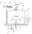
图1是用于根据本发明实施例形成非晶碳膜的沉积设备的示意性横截面图,即PECVD(Plasma Enhanced Chemical Vapor Deposition,等离子体增强型化学气相沉积)设备的示意性横截面图。1 is a schematic cross-sectional view of a deposition device for forming an amorphous carbon film according to an embodiment of the present invention, that is, a schematic cross-sectional view of a PECVD (Plasma Enhanced Chemical Vapor Deposition, plasma enhanced chemical vapor deposition) device.
参看图1,沉积设备包含真空单元10、腔室20、气体供应器30和功率供应器40。Referring to FIG. 1 , the deposition apparatus includes a
所述真空单元10包含泵11(例如涡轮分子泵)、阀12和排气管13。另外,真空单元10保持腔室20的内部处于真空状态,使得合适地执行沉积。另外,真空单元10用于排空遗留在腔室20中的未反应气体。The
腔室20具有对应于衬底1的形状的长方体或圆柱体形状,且为沉积过程提供空间。另外,腔室包含衬底支撑件21、喷头22、压力测量单元23、衬垫24和泵盘25。衬底支撑件21设置在腔室20的下部处,且用于形成非晶碳膜的衬底1放置在衬底支撑件上。从气体供应器30将源气体供应到喷头22,且从功率供应器40将射频功率供应到喷头22。因此,从气体供应器30供应到喷头且接着由喷头22注射的源气体被从功率供应器40供应的射频功率离子化,且接着沉积在衬底1上。另外,喷头22与腔室20的内壁隔离。压力测量单元23测量腔室20内部的压力。由压力测量单元23测得的压力对阀12的打开度进行控制。因而,能够将腔室20内部的压力维持在预定压力。在腔室20的内壁上提供衬垫24,以便防止腔室20的内壁(其由铝制成)被等离子体破坏或以防止反应物沉积在腔室20的内壁上。优选的是,衬垫由陶瓷材料制成。泵盘25允许残余气体凭借泵11通过排气管13均匀地排出。泵盘25具有带多个孔的盘形状。The
气体供应器30包含汽化器31和气体供应管32。汽化器31将液相反应源汽化以在衬底1上形成非晶碳膜。经汽化的反应源和包含氩气的运载气体通过气体供应管32供应到腔室20。The
功率供应器40包含射频产生器41和匹配单元42。另外,功率供应器40将射频功率施加到喷头22,使得源气体被离子化且沉积在衬底1上。射频产生器41产生在800到2000W范围内具有13.56MHz的射频功率。The
同时,除了包含射频产生器41和匹配单元42的功率供应器40用以产生射频功率之外,沉积设备还可包含另一功率供应器(未图示)用以产生低频功率,其包含低频产生器(未图示)和匹配单元(未图示)。所述产生低频功率的功率供应器可连接到腔室20的下部(例如,衬底支撑件21)。当供应低频功率时,源气体离子的线性得以改进。因而,沉积在衬底1上的非晶碳膜的均匀性得以改进,且薄膜的应力得以减小,借此薄膜的质量得以改进。低频功率产生器产生在150到400W范围内具有400kHz的低频功率。At the same time, in addition to the
下文将描述根据本发明实施例的使用前述沉积设备形成非晶碳膜的方法。Hereinafter, a method of forming an amorphous carbon film using the foregoing deposition apparatus according to an embodiment of the present invention will be described.
首先,将上面形成有预定结构的衬底1放置在衬底支撑件21上且接着将其加载到腔室20中。在腔室20的内部被真空单元10排空之后,由气体供应器30和喷头22将反应源汽化并进行注射。在此情况下,在腔室20中,从功率供应器40将射频(RF)功率施加到喷头12。在腔室20中由于射频功率而产生等离子体,且反应源被离子化并移动到衬底1。另外,低频功率被进一步施加到衬底支撑件21,使得离子的线性由于低频功率而得以改进。因此,在衬底1上形成具有改进的质量和均匀性的非晶碳膜。First, a substrate 1 on which a predetermined structure is formed is placed on a
在此情况下,液态碳氢化合物经汽化以用作用以形成非晶碳膜的反应源。液态碳氢化合物可通过汽化转换为气体,且依据反应条件而进一步转换为等离子体状态。本发明示范性实施例中所使用的碳氢化合物是链状结构,包含一个双键,且由碳原子和氢原子组成。此类碳氢化合物包含从由以下各物组成的群组中选出的一者:己烯(C6H12)、壬烯(C9H18)、十二烯(C12H24)、十五烯(C15H30)和其组合,其分别由化学式1到4表示。与其它碳氢化合物相比,可容易地控制上述碳氢化合物的沉积速率、蚀刻选择性、折射率(n)、光吸收系数(k)和应力特征。另外,与其它碳氢化合物相比,当使用上述碳氢化合物时会产生较少量的反应副产物,从而较少量的副产物粘附到腔室20的内壁。因此,可简化用于从腔室20的内壁移除污染物的过程。In this case, liquid hydrocarbon is vaporized to serve as a reaction source to form an amorphous carbon film. Liquid hydrocarbons can be converted to gas by vaporization and further converted to a plasma state depending on the reaction conditions. The hydrocarbon used in the exemplary embodiments of the present invention is a chain structure, contains one double bond, and consists of carbon atoms and hydrogen atoms. Such hydrocarbons include one selected from the group consisting of hexene (C6 H12 ), nonene (C9 H18 ), dodecene (C12 H24 ), Pentacene (C15 H30 ) and combinations thereof, which are represented by Chemical Formulas 1 to 4, respectively. The deposition rate, etch selectivity, refractive index (n), light absorption coefficient (k), and stress characteristics of the above hydrocarbons can be easily controlled compared to other hydrocarbons. In addition, a smaller amount of reaction by-products are generated when the above-mentioned hydrocarbons are used as compared to other hydrocarbons, so that a smaller amount of by-products adheres to the inner wall of the
[化学式1][chemical formula 1]
[化学式2][chemical formula 2]

[化学式3][chemical formula 3]

[化学式4][chemical formula 4]

另外,包含氩气、氦气等的惰性气体用作等离子体产生气体和用以运载源气体的运载气体。在此情况下,以在0.3到0.8g/min范围内的流动速率供应液相的碳氢化合物。明确地说,氩气(用作运载气体的惰性气体之一)用以改进等离子体的均匀性、非晶碳膜的膜厚度和质量的均匀性。此外,氢气(H2)或氨气(NH3)可用以控制非晶碳膜中的氢的浓度。In addition, an inert gas including argon, helium, or the like is used as a plasma generation gas and a carrier gas to carry a source gas. In this case, the hydrocarbon in the liquid phase is supplied at a flow rate in the range of 0.3 to 0.8 g/min. Specifically, argon (one of the inert gases used as carrier gas) was used to improve the uniformity of plasma, the uniformity of film thickness and quality of the amorphous carbon film. In addition, hydrogen gas (H2 ) or ammonia gas (NH3 ) may be used to control the concentration of hydrogen in the amorphous carbon film.
另外,用以形成非晶碳膜的所需条件包含在800到2000W范围内具有13.56MHz的射频功率、在4.5到8托范围内的腔室压力、300到550℃的温度和在250到400密耳范围内的衬底与喷头之间的距离。在此情况下,以在15到80
当射频功率较低时,沉积速率下降。因而,不沉积膜。当射频功率较高时,沉积速率增加。因此,膜没有被密集地沉积。因此,膜的质量变差。当待施加的反应源的量较小时,沉积速率下降。因此,不能在所需时间内沉积具有所需厚度的膜。当待供应的反应源的量较大时,沉积速率增加。因此,膜没有被密集地沉积。因此,膜的质量变差,且产生颗粒。另外,如果喷头与衬底之间的距离较小,那么出现飞弧。当喷头与衬底之间的距离较大时,沉积速率下降。因而,膜没有被沉积。此外,当压力较高时,产生颗粒。当压力较低时,折射率和光吸收系数的特征变差。当温度较低时,膜的质量变差。当温度较高时,折射率和光吸收系数的特征变差。因此,需要如上所述般地调节用以形成非晶碳膜的条件。When the RF power is lower, the deposition rate decreases. Thus, no film is deposited. When the RF power is higher, the deposition rate increases. Therefore, the film is not densely deposited. Therefore, the quality of the film deteriorates. When the amount of reactive source to be applied is small, the deposition rate decreases. Therefore, a film having a desired thickness cannot be deposited within a desired time. When the amount of the reaction source to be supplied is larger, the deposition rate increases. Therefore, the film is not densely deposited. Therefore, the quality of the film deteriorates, and particles are generated. Additionally, arcing occurs if the distance between the showerhead and the substrate is small. The deposition rate drops when the distance between the showerhead and the substrate is larger. Thus, the film was not deposited. In addition, when the pressure is high, particles are generated. When the pressure is low, the characteristics of the refractive index and light absorption coefficient deteriorate. When the temperature is lower, the quality of the film deteriorates. When the temperature is higher, the characteristics of the refractive index and the light absorption coefficient deteriorate. Therefore, it is necessary to adjust the conditions for forming the amorphous carbon film as described above.
同时,非晶碳膜含有氢,且碳与氢的比率可控制在9∶1到6∶4的范围内,这可通过控制射频功率、碳氢化合物的量、腔室压力和沉积温度来实现。也就是说,为了增加氢的比率,降低射频功率和温度,增加腔室压力,且增加碳氢化合物的量。相反,为了降低氢的比率,增加射频功率和温度,降低腔室压力,且降低碳氢化合物的量。At the same time, the amorphous carbon film contains hydrogen, and the ratio of carbon to hydrogen can be controlled in the range of 9:1 to 6:4, which can be achieved by controlling the RF power, the amount of hydrocarbons, the chamber pressure and the deposition temperature . That is, to increase the ratio of hydrogen, the RF power and temperature are decreased, the chamber pressure is increased, and the amount of hydrocarbons is increased. Conversely, to decrease the ratio of hydrogen, the RF power and temperature are increased, the chamber pressure is decreased, and the amount of hydrocarbons is decreased.
在随后蚀刻过程中依据碳与氢的比率来调节上述非晶碳膜相对于底层的蚀刻选择性。上述非晶碳膜相对于氧化物膜(SiO2)的蚀刻选择性在1∶5到1∶40的范围内,且上述非晶碳膜相对于氮化物膜(Si3N4)的蚀刻选择性在1∶1到1∶20的范围内。The etch selectivity of the above-mentioned amorphous carbon film relative to the underlying layer is adjusted according to the ratio of carbon to hydrogen in the subsequent etching process. The etching selectivity of the above-mentioned amorphous carbon film to the oxide film (SiO2 ) is in the range of 1:5 to 1:40, and the etching selectivity of the above-mentioned amorphous carbon film to the nitride film (Si3 N4 ) is Sex is in the range of 1:1 to 1:20.
另外,根据碳与氢的比率来控制非晶碳膜的折射率(n)和光吸收系数(k)。随着氢的比率增加,非晶碳膜的折射率(n)和光吸收系数(k)减小。举例来说,非晶碳膜的折射率(n)可控制在1.7到2.2的范围内,且非晶碳膜的光吸收系数(k)可控制在0.1到0.5的范围内。In addition, the refractive index (n) and light absorption coefficient (k) of the amorphous carbon film are controlled according to the ratio of carbon to hydrogen. As the ratio of hydrogen increases, the refractive index (n) and light absorption coefficient (k) of the amorphous carbon film decrease. For example, the refractive index (n) of the amorphous carbon film can be controlled within a range of 1.7 to 2.2, and the light absorption coefficient (k) of the amorphous carbon film can be controlled within a range of 0.1 to 0.5.
如上所述,可根据处理条件来控制非晶碳膜的应力、折射率(n)、光吸收系数(k)和沉积速率,所述处理条件例如为射频功率、待供应的反应源的量和喷头与衬底之间的距离。下文将通过本发明的随后实例来描述非晶碳膜的特征。图2A到2D是根据本发明第一实例说明非晶碳膜的特征依据射频功率而变化的图表。图3A到3D是根据本发明第二实例说明非晶碳膜的特征依据待施加的反应源的量而变化的图表。图4A到4D是根据本发明第三实例说明非晶碳膜的特征依据喷头与衬底之间的距离而变化的图表。这些图表绘示非晶碳膜的特征在最佳条件下的变化。As described above, the stress, refractive index (n), light absorption coefficient (k), and deposition rate of the amorphous carbon film can be controlled according to processing conditions such as radio frequency power, the amount of reaction source to be supplied, and The distance between the showerhead and the substrate. The characteristics of the amorphous carbon film will be described below through subsequent examples of the present invention. 2A to 2D are graphs illustrating changes in characteristics of an amorphous carbon film according to RF power according to a first example of the present invention. 3A to 3D are graphs illustrating changes in characteristics of an amorphous carbon film depending on the amount of a reactive source to be applied according to a second example of the present invention. 4A to 4D are graphs illustrating changes in characteristics of an amorphous carbon film according to a distance between a showerhead and a substrate according to a third example of the present invention. These graphs show the variation of the characteristics of the amorphous carbon film under optimal conditions.
第一实例:非晶碳膜的特征依据射频功率的变化First Example: Characterization of Amorphous Carbon Films as a Function of RF Power
在本发明的第一实例中,通过在7托的压力和550℃的温度下,同时射频功率在900到2000W的范围内变化,以0.8g/min的流动速率供应己烯(C6H12),以300sccm的流动速率供应氩气并以800sccm的流动速率供应氦气而形成非晶碳膜。另外,在喷头与衬底之间维持350密耳的距离。图2A到2D分别说明非晶碳膜的应力、折射率(n)、光吸收系数(k)和沉积速率依据射频功率的变化。In the first example of the present invention, hexene (C6 H12 ), argon gas was supplied at a flow rate of 300 sccm and helium gas was supplied at a flow rate of 800 sccm to form an amorphous carbon film. Additionally, a distance of 350 mils was maintained between the showerhead and the substrate. 2A to 2D illustrate the variation of stress, refractive index (n), light absorption coefficient (k) and deposition rate of an amorphous carbon film as a function of RF power, respectively.
图2A是说明非晶碳膜的应力依据射频功率而变化的图表。参看图2A,随着射频功率增加,应力略微增加且接着在射频功率变成1600W之后显著减小。FIG. 2A is a graph illustrating stress variation of an amorphous carbon film as a function of radio frequency power. Referring to FIG. 2A , as the RF power increased, the stress slightly increased and then decreased significantly after the RF power became 1600W.
图2B是说明非晶碳膜的折射率(n)依据射频功率而变化的图表。参看图2B,随着射频功率增加,折射率(n)减小。FIG. 2B is a graph illustrating the change in refractive index (n) of an amorphous carbon film as a function of RF power. Referring to Figure 2B, as the RF power increases, the refractive index (n) decreases.
图2C是说明非晶碳膜的光吸收系数(k)依据射频功率而变化的图表。参看图2C,随着射频功率增加,光吸收系数(k)逐渐减小,且接着在1200到1600W的范围内显著减小。然而,射频功率在1600W以上的进一步增加导致光吸收系数(k)的增加。FIG. 2C is a graph illustrating the light absorption coefficient (k) of an amorphous carbon film as a function of radio frequency power. Referring to FIG. 2C, as the RF power increases, the light absorption coefficient (k) decreases gradually, and then decreases significantly in the range of 1200 to 1600W. However, a further increase in RF power above 1600 W resulted in an increase in the optical absorption coefficient (k).
图2D是说明非晶碳膜的沉积速率(
从本发明第一实例中了解到,可基于射频功率来改变应力、折射率(n)、光吸收系数(k)和沉积速率。随着射频功率增加,折射率(n)减小,且沉积速率增加。另外,随着射频功率增加,应力增加且接着在射频功率变成1600W之后显著减小。此外,随着射频功率增加,光吸收系数(k)显著减小且接着在射频功率变成1600W之后逐渐增加。As learned from the first example of the present invention, stress, refractive index (n), light absorption coefficient (k) and deposition rate can be varied based on RF power. As the RF power increases, the refractive index (n) decreases and the deposition rate increases. In addition, as the RF power increased, the stress increased and then decreased significantly after the RF power became 1600W. Furthermore, as the RF power increased, the light absorption coefficient (k) decreased significantly and then gradually increased after the RF power became 1600W.
根据本发明第一实例的非晶碳膜具有在1.84到1.89范围内的折射率(n)和在0.36到0.41范围内的光吸收系数(k)。因此,认为非晶碳膜具有作为用于制造半导体装置的过程中的硬掩模膜或抗反射膜的优良光学特征。The amorphous carbon film according to the first example of the present invention has a refractive index (n) in the range of 1.84 to 1.89 and a light absorption coefficient (k) in the range of 0.36 to 0.41. Therefore, the amorphous carbon film is considered to have excellent optical characteristics as a hard mask film or an antireflection film used in the process of manufacturing a semiconductor device.
第二实例:非晶碳膜的特征依据待供应的反应源的量的变化Second example: change of characteristics of amorphous carbon film depending on the amount of reaction source to be supplied
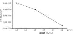
在本发明的第二实例中,通过在7托的压力和550℃的温度下,同时施加1600W的射频功率,以在0.3到0.8g/min范围内的流动速率供应己烯(C6H12),以300sccm的流动速率供应氩气并以200sccm的流动速率供应氦气而形成非晶碳膜。另外,在喷头与衬底之间维持320密耳的距离。在此情况下,图3A到3D分别说明非晶碳膜的应力、折射率(n)、光吸收系数(k)和沉积速率依据待供应的反应源的量的变化。In a second example of the present invention, hexene (C6 H12 ), argon gas was supplied at a flow rate of 300 sccm and helium gas was supplied at a flow rate of 200 sccm to form an amorphous carbon film. Additionally, a distance of 320 mils was maintained between the showerhead and the substrate. In this case, FIGS. 3A to 3D respectively illustrate changes in stress, refractive index (n), light absorption coefficient (k) and deposition rate of the amorphous carbon film depending on the amount of the reaction source to be supplied.
图3A是说明非晶碳膜的应力依据待供应的反应源的量而变化的图表。参看图3A,随着待供应的反应源的量增加,应力减小。FIG. 3A is a graph illustrating a change in stress of an amorphous carbon film depending on the amount of a reaction source to be supplied. Referring to FIG. 3A, as the amount of the reaction source to be supplied increases, the stress decreases.
图3B是说明非晶碳膜的折射率(n)依据待供应的反应源的量而变化的图表。参看图3B,随着待供应的反应源的量增加,折射率(n)减小。FIG. 3B is a graph illustrating changes in the refractive index (n) of an amorphous carbon film depending on the amount of a reaction source to be supplied. Referring to FIG. 3B, as the amount of the reaction source to be supplied increases, the refractive index (n) decreases.
图3C是说明非晶碳膜的光吸收系数(k)依据待供应的反应源的量而变化的图表。参看图3C,随着待供应的反应源的量增加,光吸收系数(k)减小。FIG. 3C is a graph illustrating a change in the light absorption coefficient (k) of an amorphous carbon film depending on the amount of a reaction source to be supplied. Referring to FIG. 3C, as the amount of the reaction source to be supplied increases, the light absorption coefficient (k) decreases.
图3D是说明非晶碳膜的沉积速率(/sec)依据待供应的反应源的量而变化的图表。参看图3D,随着待供应的反应源的量增加,沉积速率增加。Figure 3D is a graph illustrating the deposition rate of the amorphous carbon film ( /sec) is a graph that varies depending on the amount of reaction source to be supplied. Referring to FIG. 3D , as the amount of reaction source to be supplied increases, the deposition rate increases.
因此,从本发明第二实例中了解到,可依据待供应的反应源的量来改变应力、折射率(n)、光吸收系数(k)和沉积速率。随着射频功率增加,折射率(n)减小,且沉积速率增加。另外,随着待供应的反应源的量增加,应力、折射率(n)和光吸收系数(k)减小,且沉积速率增加。Therefore, it is understood from the second example of the present invention that the stress, the refractive index (n), the light absorption coefficient (k) and the deposition rate can be changed depending on the amount of the reaction source to be supplied. As the RF power increases, the refractive index (n) decreases and the deposition rate increases. In addition, as the amount of reaction sources to be supplied increases, stress, refractive index (n), and light absorption coefficient (k) decrease, and the deposition rate increases.
根据本发明第二实例的非晶碳膜具有在1.86到1.91范围内的折射率(n)和在0.36到0.41范围内的光吸收系数(k)。因此,认为非晶碳膜具有作为用于制造半导体装置的过程中的硬掩模膜或抗反射膜的优良光学特征。The amorphous carbon film according to the second example of the present invention has a refractive index (n) in the range of 1.86 to 1.91 and a light absorption coefficient (k) in the range of 0.36 to 0.41. Therefore, the amorphous carbon film is considered to have excellent optical characteristics as a hard mask film or an antireflection film used in the process of manufacturing a semiconductor device.
第三实例:非晶碳膜的特征依据喷头与衬底之间的距离的变化Example 3: Characteristics of an amorphous carbon film depending on the distance between the shower head and the substrate
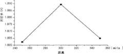
在本发明的第三实例中,通过在7托的压力和550℃的温度下,同时施加1600W的射频功率,以0.8g/min的流动速率供应己烯(C6H12),以300sccm的流动速率供应氩气并以800sccm的流动速率供应氦气而形成非晶碳膜。另外,喷头与衬底之间的距离在250到350密耳的范围内变化。在此情况下,图4A到4D分别说明非晶碳膜的应力、折射率(n)、光吸收系数(k)和沉积速率依据喷头与衬底之间的距离的变化。In the third example of the present invention, hexene (C6 H12 ) was supplied at a flow rate of 0.8 g/min at a pressure of 7 Torr and a temperature of 550° C. at a rate of 300 sccm by simultaneously applying a radio frequency power of 1600 W. Argon gas was supplied at a flow rate and helium gas was supplied at a flow rate of 800 sccm to form an amorphous carbon film. Additionally, the distance between the showerhead and the substrate was varied in the range of 250 to 350 mils. In this case, FIGS. 4A to 4D illustrate changes in stress, refractive index (n), light absorption coefficient (k), and deposition rate of the amorphous carbon film according to the distance between the shower head and the substrate, respectively.
图4A是说明非晶碳膜的应力依据喷头与衬底之间的距离而变化的图表。参看图4A,随着喷头与衬底之间的距离变大,应力减小。正(+)应力是拉伸应力,且负(-)应力是压缩应力。随着喷头与衬底之间的距离变大,应力从拉伸应力转变为压缩应力。FIG. 4A is a graph illustrating the change in stress of an amorphous carbon film depending on the distance between the showerhead and the substrate. Referring to FIG. 4A, as the distance between the showerhead and the substrate becomes larger, the stress decreases. Positive (+) stress is tensile stress, and negative (-) stress is compressive stress. As the distance between the showerhead and the substrate increases, the stress changes from tensile stress to compressive stress.
图4B是说明非晶碳膜的折射率(n)依据喷头与衬底之间的距离而变化的图表。参看图4B,随着喷头与衬底之间的距离变大,折射率(n)增加且接着在距离变成300密耳之后减小。FIG. 4B is a graph illustrating the change in the refractive index (n) of an amorphous carbon film depending on the distance between the showerhead and the substrate. Referring to FIG. 4B, as the distance between the showerhead and the substrate becomes larger, the refractive index (n) increases and then decreases after the distance becomes 300 mils.
图4C是说明非晶碳膜的光吸收系数(k)依据喷头与衬底之间的距离而变化的图表。参看图4C,随着喷头与衬底之间的距离变大,光吸收系数(k)显著增加且接着在距离变成300密耳之后逐渐减小。4C is a graph illustrating the light absorption coefficient (k) of an amorphous carbon film as a function of the distance between the showerhead and the substrate. Referring to FIG. 4C , as the distance between the showerhead and the substrate became larger, the light absorption coefficient (k) increased significantly and then gradually decreased after the distance became 300 mils.
图4D是说明非晶碳膜的沉积速率(
从本发明第三实例中了解到,可依据喷头与衬底之间的距离来改变应力、折射率(n)、光吸收系数(k)和沉积速率。随着喷头与衬底之间的距离变大,应力和沉积速率减小。另外,随着喷头与衬底之间的距离变大,折射率(n)增加且接着在距离变成300密耳之后减小。此外,随着喷头与衬底之间的距离增加,光吸收系数(k)显著增加且接着在距离变成300密耳之后逐渐减小。It is understood from the third example of the present invention that stress, refractive index (n), light absorption coefficient (k) and deposition rate can be changed depending on the distance between the shower head and the substrate. As the distance between the showerhead and the substrate increases, the stress and deposition rate decrease. In addition, as the distance between the showerhead and the substrate becomes larger, the refractive index (n) increases and then decreases after the distance becomes 300 mils. Furthermore, as the distance between the showerhead and the substrate increases, the light absorption coefficient (k) increases significantly and then gradually decreases after the distance becomes 300 mils.
根据本发明第三实例的非晶碳膜具有在1.86到1.89范围内的折射率(n)和在0.36到0.41范围内的光吸收系数(k)。因此,认为非晶碳膜具有作为用于制造半导体装置的过程中的硬掩模膜或抗反射膜的优良光学特征。The amorphous carbon film according to the third example of the present invention has a refractive index (n) in the range of 1.86 to 1.89 and a light absorption coefficient (k) in the range of 0.36 to 0.41. Therefore, the amorphous carbon film is considered to have excellent optical characteristics as a hard mask film or an antireflection film used in the process of manufacturing a semiconductor device.
已在上述实例中描述了在各种处理条件下使用己烯(C6H12)而形成的非晶碳膜的特征。然而,可在各种处理条件下使用壬烯(C9H18)、十二烯(C12H24)或十五烯(C15H30)来形成具有各种特征的非晶碳膜。此外,可将其一者或一者以上混合以用于形成非晶碳膜。The characteristics of the amorphous carbon film formed using hexene (C6 H12 ) under various processing conditions have been described in the above examples. However, nonene (C9 H18 ), dodecene (C12 H24 ), or pentacene (C15 H30 ) may be used under various processing conditions to form amorphous carbon films with various characteristics. In addition, one or more of them may be mixed for forming an amorphous carbon film.
根据本发明实例使用除己烯(C6H12)之外的壬烯(C9H18)、十二烯(C12H24)或十五烯(C15H30)而形成的非晶碳膜也具有在1.7到2.2范围内(优选地,1.85到1.88)的折射率(n)和在0.1到0.5范围内(优选地,0.36到0.4)的光吸收系数(k)。Amorphous crystals formed according to the examples of the present invention using nonene (C9 H18 ), dodecene (C12 H24 ) or pentacene (C15 H30 ) in addition to hexene (C6 H12 ) The carbon film also has a refractive index (n) in the range of 1.7 to 2.2 (preferably, 1.85 to 1.88) and a light absorption coefficient (k) in the range of 0.1 to 0.5 (preferably, 0.36 to 0.4).
与如上所述的其它碳氢化合物相比,使用其具有链状结构和一个双键的碳氢化合物而形成的非晶碳膜产生较少量的反应副产物,且容易移除粘附到腔室内壁的反应副产物。也就是说,当使用具有苯环的乙苯(C8H10)或甲苯(C7H8)形成非晶碳膜时,产生大量反应副产物,且反应副产物粘附到腔室内壁。另外,即使执行清洁过程,也不容易移除反应副产物。图5A和5B绘示腔室内部的残余物。然而,当使用具有链状结构和一个双键的己烯(C6H12)形成非晶碳膜时,产生较少量的反应副产物。由于容易通过清洁过程移除所述反应副产物,因而在图6中几乎看不到残余物。The amorphous carbon film formed using a hydrocarbon having a chain structure and one double bond produces a smaller amount of reaction by-products and is easy to remove than other hydrocarbons as described above. Reaction by-products on interior walls. That is, when the amorphous carbon film is formed using ethylbenzene (C8 H10 ) or toluene (C7 H8 ) having a benzene ring, a large amount of reaction by-products are generated, and the reaction by-products adhere to the chamber inner wall. In addition, even if the cleaning process is performed, the reaction by-products are not easily removed. 5A and 5B depict the residue inside the chamber. However, when the amorphous carbon film is formed using hexene (C6 H12 ) having a chain structure and one double bond, a smaller amount of reaction by-products is generated. Since the reaction by-products are easily removed by the cleaning process, little residue is visible in FIG. 6 .
使用上述方法形成的非晶碳膜可用作制造半导体装置的方法中的硬掩模。图7A到7F是依序说明使用上述非晶碳膜制造半导体装置的方法的横截面图。根据本发明实例的非晶碳膜具有低光吸收系数。因此,可精确地图案化光敏膜而无需单独的抗反射膜。The amorphous carbon film formed using the method described above can be used as a hard mask in a method of manufacturing a semiconductor device. 7A to 7F are cross-sectional views sequentially illustrating a method of manufacturing a semiconductor device using the above-described amorphous carbon film. The amorphous carbon film according to the example of the present invention has a low light absorption coefficient. Therefore, the photosensitive film can be accurately patterned without a separate antireflection film.
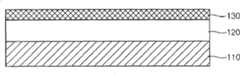
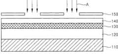
首先,如图7A所示,在半导体衬底110上形成材料层120,在所述材料层120上将形成图案。在此情况下,半导体衬底110可以是上面形成有预定结构(例如晶体管、电容器和多个金属线)以制造半导体装置的衬底。另外,材料层120可以是用于形成金属线的薄金属膜,或可以是用作夹层绝缘膜的二氧化硅膜或氮化硅膜。此外,材料层120可以是单层,或可以是其中层压有多个膜的层压层。First, as shown in FIG. 7A , a
接着,如图7B所示,通过使用上述方法在材料层120上形成非晶碳膜130。也就是说,通过使用在800到2000W范围内具有13.56MHz的射频功率由包含氩气的运载气体和包含己烯(C6H12)、壬烯(C9H18)、十二烯(C12H24)和十五烯(C15H30)中至少一者的碳氢化合物气体产生等离子体,以便将反应源离子化。因而,在金属层120上形成非晶碳膜130。在此情况下,在腔室中,在衬底与喷头之间维持在4.5到8托范围内的压力、在300到550℃范围内的温度和在250到400密耳范围内的距离,且非晶碳膜经形成为具有在15到80范围内的厚度。另外,可进一步向腔室施加在150到400W范围内具有400KHz的低频功率。如上所述般地形成的非晶碳膜130相对于材料层120具有高蚀刻选择性,且充当具有低光吸收系数(k)的硬掩模膜。Next, as shown in FIG. 7B , an
此后,如图7C所示,在非晶碳膜130上形成光敏膜140。接着,举例来说,将ArF激光A通过具有预定图案的掩模150辐射到所述光敏膜上,以便使光敏膜140曝光。另外,如图7D所示,使用显影剂来显影光敏膜140的曝光部分。Thereafter, as shown in FIG. 7C , a
随后,如图7E所示,在图案化光敏膜140用作蚀刻掩模时,蚀刻非晶碳膜130。在此情况下,使用RF等离子体或反应性离子蚀刻(RIE)来蚀刻非晶碳膜130。另外,可使用CF4等离子体、C4F8等离子体、氧气(O2)等离子体、臭氧(O3)等离子体和其组合中的一者来蚀刻所述非晶碳膜130。此外,可通过混合氧气和NF3且使用远程等离子体系统来蚀刻非晶碳膜130。Subsequently, as shown in FIG. 7E, the
接下来,如图7F所示,在光敏膜140和非晶碳膜130用作蚀刻掩模时,蚀刻材料层120。在此情况下,可依据材料层120的材料使用各种方法来蚀刻材料层120。接着,移除光敏膜140和非晶碳膜130以完成使用材料层120的图案的形成。Next, as shown in FIG. 7F , while the
非晶碳膜可在除上文提到的实例之外的制造半导体装置的方法的各种光和蚀刻过程中用作硬掩模膜。举例来说,非晶碳膜可在镶嵌过程中用作硬掩模膜。The amorphous carbon film can be used as a hard mask film in various photo and etching processes of a method of manufacturing a semiconductor device other than the above-mentioned examples. For example, an amorphous carbon film can be used as a hard mask film in a damascene process.
尽管已参看附图和优选实例描述了本发明,但本发明并不限于此,而是由所附权利要求书界定。因此,应注意,可在不脱离所附权利要求书的技术精神的情况下由所属领域的技术人员进行各种改变和修改。Although the invention has been described with reference to the drawings and preferred examples, the invention is not limited thereto but is defined by the appended claims. Therefore, it should be noted that various changes and modifications can be made by those skilled in the art without departing from the technical spirit of the appended claims.
如上所述,根据本发明实例,使用源气体形成非晶碳膜。通过将具有一个双键的链状结构碳氢化合物汽化来获得源气体。所述碳氢化合物包含液相的己烯、壬烯、十二烯、十五烯和其组合中的一者。As described above, according to an example of the present invention, an amorphous carbon film is formed using a source gas. The source gas is obtained by vaporizing chain-structure hydrocarbons having one double bond. The hydrocarbon comprises one of hexene, nonene, dodecene, pentacene, and combinations thereof in the liquid phase.
可容易地控制如上所述形成的非晶碳膜的特征(例如沉积速率、蚀刻选择性、折射率(n)、光吸收系数(k)和应力)以满足用户要求。明确地说,可精确地将折射率(n)和光吸收系数(k)控制在所需范围内,且降低折射率和光吸收系数。因而,可在不具有防止下材料层发生漫反射的抗反射膜的情况下执行光刻过程。Characteristics of the amorphous carbon film formed as described above, such as deposition rate, etch selectivity, refractive index (n), light absorption coefficient (k), and stress, can be easily controlled to meet user requirements. Specifically, the refractive index (n) and light absorption coefficient (k) can be precisely controlled within desired ranges and reduced. Thus, the photolithography process can be performed without an anti-reflection film that prevents diffuse reflection from the underlying material layer.
此外,产生少量反应副产物,且可容易地移除粘附到腔室内壁的反应副产物。从而,清洁周期和零件替换周期变得较长,这节省了时间和成本。In addition, a small amount of reaction by-products is generated, and the reaction by-products adhering to the inner wall of the chamber can be easily removed. Consequently, cleaning cycles and parts replacement cycles become longer, which saves time and costs.
另外,通过施加低频功率而改进离子的线性。为此,可在元件的梯状部分上形成非晶碳膜时抑制垂悬物的出现,这改进了阶梯覆盖率。因此,可防止蚀刻非所需的区域。Additionally, ion linearity is improved by applying low frequency power. For this reason, the occurrence of overhangs can be suppressed when the amorphous carbon film is formed on the stepped portion of the element, which improves the step coverage. Therefore, unintended regions can be prevented from being etched.
Claims (18)
Translated fromChinese
Applications Claiming Priority (3)
| Application Number | Priority Date | Filing Date | Title |
|---|---|---|---|
| KR10-2007-0049730 | 2007-05-22 | ||
| KR1020070049730AKR100777043B1 (en) | 2007-05-22 | 2007-05-22 | Amorphous carbon film formation method and semiconductor device manufacturing method using same |
| KR1020070049730 | 2007-05-22 |
Publications (2)
| Publication Number | Publication Date |
|---|---|
| CN101312126Atrue CN101312126A (en) | 2008-11-26 |
| CN101312126B CN101312126B (en) | 2010-11-17 |
Family
ID=39079928
Family Applications (1)
| Application Number | Title | Priority Date | Filing Date |
|---|---|---|---|
| CN200710153932XAExpired - Fee RelatedCN101312126B (en) | 2007-05-22 | 2007-09-14 | Method of forming amorphous carbon film and method of manufacturing semiconductor device using same |
Country Status (5)
| Country | Link |
|---|---|
| US (1) | US20080293248A1 (en) |
| JP (1) | JP2008291344A (en) |
| KR (1) | KR100777043B1 (en) |
| CN (1) | CN101312126B (en) |
| TW (1) | TW200847233A (en) |
Cited By (10)
| Publication number | Priority date | Publication date | Assignee | Title |
|---|---|---|---|---|
| CN103984212A (en)* | 2014-05-27 | 2014-08-13 | 上海华力微电子有限公司 | Method for improving exposure shape of photoresist and method for patterning semiconductor substrate |
| CN105122432A (en)* | 2013-04-19 | 2015-12-02 | 东京毅力科创株式会社 | Etching method |
| CN105448705A (en)* | 2014-06-18 | 2016-03-30 | 无锡华润上华科技有限公司 | Method for removing tiny particles on wafer oxidation film, and oxidation film |
| CN107369719A (en)* | 2017-08-25 | 2017-11-21 | 华南理工大学 | A kind of oxide thin film transistor fine copper composite construction source-drain electrode and preparation method thereof |
| CN107406979A (en)* | 2015-03-20 | 2017-11-28 | Asm国际股份有限公司 | Method for clean deposition equipment |
| CN110261256A (en)* | 2019-06-11 | 2019-09-20 | 上海大学 | A method of the measurement intrinsic deposition rate of CVD/CVI technique presoma |
| CN111448640A (en)* | 2017-12-07 | 2020-07-24 | 朗姆研究公司 | Antioxidant protective layer in chamber conditioning |
| CN112185809A (en)* | 2019-07-01 | 2021-01-05 | 美光科技公司 | Atomic implantation for reducing compressive stress |
| US12227837B2 (en) | 2017-12-15 | 2025-02-18 | Lam Research Corporation | Ex situ coating of chamber components for semiconductor processing |
| US12371781B2 (en) | 2018-10-19 | 2025-07-29 | Lam Research Corporation | In situ protective coating of chamber components for semiconductor processing |
Families Citing this family (153)
| Publication number | Priority date | Publication date | Assignee | Title |
|---|---|---|---|---|
| US7514125B2 (en)* | 2006-06-23 | 2009-04-07 | Applied Materials, Inc. | Methods to improve the in-film defectivity of PECVD amorphous carbon films |
| KR101390349B1 (en)* | 2007-11-22 | 2014-05-02 | (주)소슬 | Amorphous carbon film, method of forming the same and method of manufacturing semiconductor device using the same |
| WO2010045153A2 (en)* | 2008-10-14 | 2010-04-22 | Applied Materials, Inc. | Method for depositing conformal amorphous carbon film by plasma-enhanced chemical vapor deposition (pecvd) |
| US9324576B2 (en) | 2010-05-27 | 2016-04-26 | Applied Materials, Inc. | Selective etch for silicon films |
| JP5524132B2 (en)* | 2010-07-15 | 2014-06-18 | 東京エレクトロン株式会社 | Thin film forming apparatus cleaning method, thin film forming method, and thin film forming apparatus |
| JP5679281B2 (en)* | 2010-10-18 | 2015-03-04 | 旭化成イーマテリアルズ株式会社 | LAMINATE, AND METHOD FOR PRODUCING MOLD USING LAMINATE |
| US10283321B2 (en) | 2011-01-18 | 2019-05-07 | Applied Materials, Inc. | Semiconductor processing system and methods using capacitively coupled plasma |
| US8999856B2 (en) | 2011-03-14 | 2015-04-07 | Applied Materials, Inc. | Methods for etch of sin films |
| US9064815B2 (en) | 2011-03-14 | 2015-06-23 | Applied Materials, Inc. | Methods for etch of metal and metal-oxide films |
| US8808563B2 (en) | 2011-10-07 | 2014-08-19 | Applied Materials, Inc. | Selective etch of silicon by way of metastable hydrogen termination |
| US9511560B2 (en)* | 2012-04-13 | 2016-12-06 | Infineon Technologies Ag | Processing a sacrificial material during manufacture of a microfabricated product |
| US8679987B2 (en)* | 2012-05-10 | 2014-03-25 | Applied Materials, Inc. | Deposition of an amorphous carbon layer with high film density and high etch selectivity |
| US9267739B2 (en) | 2012-07-18 | 2016-02-23 | Applied Materials, Inc. | Pedestal with multi-zone temperature control and multiple purge capabilities |
| US9373517B2 (en) | 2012-08-02 | 2016-06-21 | Applied Materials, Inc. | Semiconductor processing with DC assisted RF power for improved control |
| US9034770B2 (en) | 2012-09-17 | 2015-05-19 | Applied Materials, Inc. | Differential silicon oxide etch |
| US9023734B2 (en) | 2012-09-18 | 2015-05-05 | Applied Materials, Inc. | Radical-component oxide etch |
| US9390937B2 (en) | 2012-09-20 | 2016-07-12 | Applied Materials, Inc. | Silicon-carbon-nitride selective etch |
| US9132436B2 (en) | 2012-09-21 | 2015-09-15 | Applied Materials, Inc. | Chemical control features in wafer process equipment |
| US8969212B2 (en) | 2012-11-20 | 2015-03-03 | Applied Materials, Inc. | Dry-etch selectivity |
| US8980763B2 (en) | 2012-11-30 | 2015-03-17 | Applied Materials, Inc. | Dry-etch for selective tungsten removal |
| US9111877B2 (en) | 2012-12-18 | 2015-08-18 | Applied Materials, Inc. | Non-local plasma oxide etch |
| US8921234B2 (en) | 2012-12-21 | 2014-12-30 | Applied Materials, Inc. | Selective titanium nitride etching |
| US10256079B2 (en) | 2013-02-08 | 2019-04-09 | Applied Materials, Inc. | Semiconductor processing systems having multiple plasma configurations |
| US9362130B2 (en) | 2013-03-01 | 2016-06-07 | Applied Materials, Inc. | Enhanced etching processes using remote plasma sources |
| US9040422B2 (en) | 2013-03-05 | 2015-05-26 | Applied Materials, Inc. | Selective titanium nitride removal |
| US20140271097A1 (en) | 2013-03-15 | 2014-09-18 | Applied Materials, Inc. | Processing systems and methods for halide scavenging |
| US9493879B2 (en) | 2013-07-12 | 2016-11-15 | Applied Materials, Inc. | Selective sputtering for pattern transfer |
| US9773648B2 (en) | 2013-08-30 | 2017-09-26 | Applied Materials, Inc. | Dual discharge modes operation for remote plasma |
| US9589799B2 (en)* | 2013-09-30 | 2017-03-07 | Lam Research Corporation | High selectivity and low stress carbon hardmask by pulsed low frequency RF power |
| US9576809B2 (en) | 2013-11-04 | 2017-02-21 | Applied Materials, Inc. | Etch suppression with germanium |
| US9520303B2 (en) | 2013-11-12 | 2016-12-13 | Applied Materials, Inc. | Aluminum selective etch |
| US9245762B2 (en) | 2013-12-02 | 2016-01-26 | Applied Materials, Inc. | Procedure for etch rate consistency |
| US9287095B2 (en) | 2013-12-17 | 2016-03-15 | Applied Materials, Inc. | Semiconductor system assemblies and methods of operation |
| US9287134B2 (en) | 2014-01-17 | 2016-03-15 | Applied Materials, Inc. | Titanium oxide etch |
| US9293568B2 (en) | 2014-01-27 | 2016-03-22 | Applied Materials, Inc. | Method of fin patterning |
| US9396989B2 (en) | 2014-01-27 | 2016-07-19 | Applied Materials, Inc. | Air gaps between copper lines |
| US9385028B2 (en) | 2014-02-03 | 2016-07-05 | Applied Materials, Inc. | Air gap process |
| US9499898B2 (en) | 2014-03-03 | 2016-11-22 | Applied Materials, Inc. | Layered thin film heater and method of fabrication |
| US9299575B2 (en) | 2014-03-17 | 2016-03-29 | Applied Materials, Inc. | Gas-phase tungsten etch |
| US9299537B2 (en) | 2014-03-20 | 2016-03-29 | Applied Materials, Inc. | Radial waveguide systems and methods for post-match control of microwaves |
| US9903020B2 (en) | 2014-03-31 | 2018-02-27 | Applied Materials, Inc. | Generation of compact alumina passivation layers on aluminum plasma equipment components |
| US9269590B2 (en) | 2014-04-07 | 2016-02-23 | Applied Materials, Inc. | Spacer formation |
| US9309598B2 (en) | 2014-05-28 | 2016-04-12 | Applied Materials, Inc. | Oxide and metal removal |
| US9406523B2 (en) | 2014-06-19 | 2016-08-02 | Applied Materials, Inc. | Highly selective doped oxide removal method |
| US9378969B2 (en)* | 2014-06-19 | 2016-06-28 | Applied Materials, Inc. | Low temperature gas-phase carbon removal |
| US20150371861A1 (en)* | 2014-06-23 | 2015-12-24 | Applied Materials, Inc. | Protective silicon oxide patterning |
| US9425058B2 (en) | 2014-07-24 | 2016-08-23 | Applied Materials, Inc. | Simplified litho-etch-litho-etch process |
| US9496167B2 (en) | 2014-07-31 | 2016-11-15 | Applied Materials, Inc. | Integrated bit-line airgap formation and gate stack post clean |
| US9378978B2 (en) | 2014-07-31 | 2016-06-28 | Applied Materials, Inc. | Integrated oxide recess and floating gate fin trimming |
| US9659753B2 (en) | 2014-08-07 | 2017-05-23 | Applied Materials, Inc. | Grooved insulator to reduce leakage current |
| US9553102B2 (en) | 2014-08-19 | 2017-01-24 | Applied Materials, Inc. | Tungsten separation |
| US9355856B2 (en) | 2014-09-12 | 2016-05-31 | Applied Materials, Inc. | V trench dry etch |
| US9355862B2 (en) | 2014-09-24 | 2016-05-31 | Applied Materials, Inc. | Fluorine-based hardmask removal |
| US9368364B2 (en) | 2014-09-24 | 2016-06-14 | Applied Materials, Inc. | Silicon etch process with tunable selectivity to SiO2 and other materials |
| US9613822B2 (en) | 2014-09-25 | 2017-04-04 | Applied Materials, Inc. | Oxide etch selectivity enhancement |
| KR20160039739A (en) | 2014-10-01 | 2016-04-12 | 삼성전자주식회사 | Method for forming hard mask layer and method for manufacturing semiconductor device using the same |
| US9966240B2 (en) | 2014-10-14 | 2018-05-08 | Applied Materials, Inc. | Systems and methods for internal surface conditioning assessment in plasma processing equipment |
| US9355922B2 (en) | 2014-10-14 | 2016-05-31 | Applied Materials, Inc. | Systems and methods for internal surface conditioning in plasma processing equipment |
| US11637002B2 (en) | 2014-11-26 | 2023-04-25 | Applied Materials, Inc. | Methods and systems to enhance process uniformity |
| US9299583B1 (en) | 2014-12-05 | 2016-03-29 | Applied Materials, Inc. | Aluminum oxide selective etch |
| US10224210B2 (en) | 2014-12-09 | 2019-03-05 | Applied Materials, Inc. | Plasma processing system with direct outlet toroidal plasma source |
| US10573496B2 (en) | 2014-12-09 | 2020-02-25 | Applied Materials, Inc. | Direct outlet toroidal plasma source |
| US9502258B2 (en) | 2014-12-23 | 2016-11-22 | Applied Materials, Inc. | Anisotropic gap etch |
| US9343272B1 (en) | 2015-01-08 | 2016-05-17 | Applied Materials, Inc. | Self-aligned process |
| US11257693B2 (en) | 2015-01-09 | 2022-02-22 | Applied Materials, Inc. | Methods and systems to improve pedestal temperature control |
| US9373522B1 (en) | 2015-01-22 | 2016-06-21 | Applied Mateials, Inc. | Titanium nitride removal |
| US9449846B2 (en) | 2015-01-28 | 2016-09-20 | Applied Materials, Inc. | Vertical gate separation |
| US9728437B2 (en) | 2015-02-03 | 2017-08-08 | Applied Materials, Inc. | High temperature chuck for plasma processing systems |
| US20160225652A1 (en) | 2015-02-03 | 2016-08-04 | Applied Materials, Inc. | Low temperature chuck for plasma processing systems |
| US9640385B2 (en)* | 2015-02-16 | 2017-05-02 | Applied Materials, Inc. | Gate electrode material residual removal process |
| US9881805B2 (en) | 2015-03-02 | 2018-01-30 | Applied Materials, Inc. | Silicon selective removal |
| US9646818B2 (en)* | 2015-03-23 | 2017-05-09 | Applied Materials, Inc. | Method of forming planar carbon layer by applying plasma power to a combination of hydrocarbon precursor and hydrogen-containing precursor |
| US9741593B2 (en) | 2015-08-06 | 2017-08-22 | Applied Materials, Inc. | Thermal management systems and methods for wafer processing systems |
| US9691645B2 (en) | 2015-08-06 | 2017-06-27 | Applied Materials, Inc. | Bolted wafer chuck thermal management systems and methods for wafer processing systems |
| US9349605B1 (en) | 2015-08-07 | 2016-05-24 | Applied Materials, Inc. | Oxide etch selectivity systems and methods |
| US10504700B2 (en) | 2015-08-27 | 2019-12-10 | Applied Materials, Inc. | Plasma etching systems and methods with secondary plasma injection |
| US10522371B2 (en) | 2016-05-19 | 2019-12-31 | Applied Materials, Inc. | Systems and methods for improved semiconductor etching and component protection |
| US10504754B2 (en) | 2016-05-19 | 2019-12-10 | Applied Materials, Inc. | Systems and methods for improved semiconductor etching and component protection |
| US9865484B1 (en) | 2016-06-29 | 2018-01-09 | Applied Materials, Inc. | Selective etch using material modification and RF pulsing |
| US10062575B2 (en) | 2016-09-09 | 2018-08-28 | Applied Materials, Inc. | Poly directional etch by oxidation |
| US10629473B2 (en) | 2016-09-09 | 2020-04-21 | Applied Materials, Inc. | Footing removal for nitride spacer |
| US10062585B2 (en) | 2016-10-04 | 2018-08-28 | Applied Materials, Inc. | Oxygen compatible plasma source |
| US10546729B2 (en) | 2016-10-04 | 2020-01-28 | Applied Materials, Inc. | Dual-channel showerhead with improved profile |
| US9934942B1 (en) | 2016-10-04 | 2018-04-03 | Applied Materials, Inc. | Chamber with flow-through source |
| US9721789B1 (en) | 2016-10-04 | 2017-08-01 | Applied Materials, Inc. | Saving ion-damaged spacers |
| US10062579B2 (en) | 2016-10-07 | 2018-08-28 | Applied Materials, Inc. | Selective SiN lateral recess |
| US9947549B1 (en) | 2016-10-10 | 2018-04-17 | Applied Materials, Inc. | Cobalt-containing material removal |
| US10163696B2 (en) | 2016-11-11 | 2018-12-25 | Applied Materials, Inc. | Selective cobalt removal for bottom up gapfill |
| US9768034B1 (en) | 2016-11-11 | 2017-09-19 | Applied Materials, Inc. | Removal methods for high aspect ratio structures |
| US10026621B2 (en) | 2016-11-14 | 2018-07-17 | Applied Materials, Inc. | SiN spacer profile patterning |
| US10242908B2 (en) | 2016-11-14 | 2019-03-26 | Applied Materials, Inc. | Airgap formation with damage-free copper |
| US10566206B2 (en) | 2016-12-27 | 2020-02-18 | Applied Materials, Inc. | Systems and methods for anisotropic material breakthrough |
| US10403507B2 (en) | 2017-02-03 | 2019-09-03 | Applied Materials, Inc. | Shaped etch profile with oxidation |
| US10431429B2 (en) | 2017-02-03 | 2019-10-01 | Applied Materials, Inc. | Systems and methods for radial and azimuthal control of plasma uniformity |
| US10043684B1 (en) | 2017-02-06 | 2018-08-07 | Applied Materials, Inc. | Self-limiting atomic thermal etching systems and methods |
| US10319739B2 (en) | 2017-02-08 | 2019-06-11 | Applied Materials, Inc. | Accommodating imperfectly aligned memory holes |
| US10943834B2 (en) | 2017-03-13 | 2021-03-09 | Applied Materials, Inc. | Replacement contact process |
| US10319649B2 (en) | 2017-04-11 | 2019-06-11 | Applied Materials, Inc. | Optical emission spectroscopy (OES) for remote plasma monitoring |
| JP7176860B6 (en) | 2017-05-17 | 2022-12-16 | アプライド マテリアルズ インコーポレイテッド | Semiconductor processing chamber to improve precursor flow |
| US11276559B2 (en) | 2017-05-17 | 2022-03-15 | Applied Materials, Inc. | Semiconductor processing chamber for multiple precursor flow |
| US11276590B2 (en) | 2017-05-17 | 2022-03-15 | Applied Materials, Inc. | Multi-zone semiconductor substrate supports |
| US10497579B2 (en) | 2017-05-31 | 2019-12-03 | Applied Materials, Inc. | Water-free etching methods |
| US10049891B1 (en) | 2017-05-31 | 2018-08-14 | Applied Materials, Inc. | Selective in situ cobalt residue removal |
| US10920320B2 (en) | 2017-06-16 | 2021-02-16 | Applied Materials, Inc. | Plasma health determination in semiconductor substrate processing reactors |
| US10541246B2 (en) | 2017-06-26 | 2020-01-21 | Applied Materials, Inc. | 3D flash memory cells which discourage cross-cell electrical tunneling |
| US10727080B2 (en) | 2017-07-07 | 2020-07-28 | Applied Materials, Inc. | Tantalum-containing material removal |
| US10541184B2 (en) | 2017-07-11 | 2020-01-21 | Applied Materials, Inc. | Optical emission spectroscopic techniques for monitoring etching |
| US10354889B2 (en) | 2017-07-17 | 2019-07-16 | Applied Materials, Inc. | Non-halogen etching of silicon-containing materials |
| US10170336B1 (en) | 2017-08-04 | 2019-01-01 | Applied Materials, Inc. | Methods for anisotropic control of selective silicon removal |
| US10043674B1 (en) | 2017-08-04 | 2018-08-07 | Applied Materials, Inc. | Germanium etching systems and methods |
| US10297458B2 (en) | 2017-08-07 | 2019-05-21 | Applied Materials, Inc. | Process window widening using coated parts in plasma etch processes |
| US10804109B2 (en) | 2017-10-03 | 2020-10-13 | Mattson Technology, Inc. | Surface treatment of silicon and carbon containing films by remote plasma with organic precursors |
| US10128086B1 (en) | 2017-10-24 | 2018-11-13 | Applied Materials, Inc. | Silicon pretreatment for nitride removal |
| US10283324B1 (en) | 2017-10-24 | 2019-05-07 | Applied Materials, Inc. | Oxygen treatment for nitride etching |
| US10256112B1 (en) | 2017-12-08 | 2019-04-09 | Applied Materials, Inc. | Selective tungsten removal |
| US10903054B2 (en) | 2017-12-19 | 2021-01-26 | Applied Materials, Inc. | Multi-zone gas distribution systems and methods |
| US11328909B2 (en) | 2017-12-22 | 2022-05-10 | Applied Materials, Inc. | Chamber conditioning and removal processes |
| US10854426B2 (en) | 2018-01-08 | 2020-12-01 | Applied Materials, Inc. | Metal recess for semiconductor structures |
| US10679870B2 (en) | 2018-02-15 | 2020-06-09 | Applied Materials, Inc. | Semiconductor processing chamber multistage mixing apparatus |
| US10964512B2 (en) | 2018-02-15 | 2021-03-30 | Applied Materials, Inc. | Semiconductor processing chamber multistage mixing apparatus and methods |
| TWI766433B (en) | 2018-02-28 | 2022-06-01 | 美商應用材料股份有限公司 | Systems and methods to form airgaps |
| US10593560B2 (en) | 2018-03-01 | 2020-03-17 | Applied Materials, Inc. | Magnetic induction plasma source for semiconductor processes and equipment |
| US10319600B1 (en) | 2018-03-12 | 2019-06-11 | Applied Materials, Inc. | Thermal silicon etch |
| US10497573B2 (en) | 2018-03-13 | 2019-12-03 | Applied Materials, Inc. | Selective atomic layer etching of semiconductor materials |
| US10573527B2 (en) | 2018-04-06 | 2020-02-25 | Applied Materials, Inc. | Gas-phase selective etching systems and methods |
| SG11202009406RA (en)* | 2018-04-09 | 2020-10-29 | Applied Materials Inc | Carbon hard masks for patterning applications and methods related thereto |
| US10490406B2 (en) | 2018-04-10 | 2019-11-26 | Appled Materials, Inc. | Systems and methods for material breakthrough |
| US11387111B2 (en) | 2018-04-13 | 2022-07-12 | Mattson Technology, Inc. | Processing of workpieces with reactive species generated using alkyl halide |
| US10699879B2 (en) | 2018-04-17 | 2020-06-30 | Applied Materials, Inc. | Two piece electrode assembly with gap for plasma control |
| US10886137B2 (en) | 2018-04-30 | 2021-01-05 | Applied Materials, Inc. | Selective nitride removal |
| KR102363121B1 (en) | 2018-06-11 | 2022-02-15 | 매슨 테크놀로지 인크 | Generation of hydrogen-reactive species for processing of workpieces |
| US10755941B2 (en) | 2018-07-06 | 2020-08-25 | Applied Materials, Inc. | Self-limiting selective etching systems and methods |
| US10872778B2 (en) | 2018-07-06 | 2020-12-22 | Applied Materials, Inc. | Systems and methods utilizing solid-phase etchants |
| US10672642B2 (en) | 2018-07-24 | 2020-06-02 | Applied Materials, Inc. | Systems and methods for pedestal configuration |
| US11049755B2 (en) | 2018-09-14 | 2021-06-29 | Applied Materials, Inc. | Semiconductor substrate supports with embedded RF shield |
| US10892198B2 (en) | 2018-09-14 | 2021-01-12 | Applied Materials, Inc. | Systems and methods for improved performance in semiconductor processing |
| US11062887B2 (en) | 2018-09-17 | 2021-07-13 | Applied Materials, Inc. | High temperature RF heater pedestals |
| US11417534B2 (en) | 2018-09-21 | 2022-08-16 | Applied Materials, Inc. | Selective material removal |
| US11682560B2 (en) | 2018-10-11 | 2023-06-20 | Applied Materials, Inc. | Systems and methods for hafnium-containing film removal |
| CN112313777B (en) | 2018-10-15 | 2024-08-27 | 玛特森技术公司 | Method for selective hydrophilic surface treatment using ozone |
| US11121002B2 (en) | 2018-10-24 | 2021-09-14 | Applied Materials, Inc. | Systems and methods for etching metals and metal derivatives |
| CN118471789A (en) | 2018-11-16 | 2024-08-09 | 玛特森技术公司 | Chamber polishing to improve etch uniformity by reducing chemical composition |
| US11437242B2 (en) | 2018-11-27 | 2022-09-06 | Applied Materials, Inc. | Selective removal of silicon-containing materials |
| US10403492B1 (en) | 2018-12-11 | 2019-09-03 | Mattson Technology, Inc. | Integration of materials removal and surface treatment in semiconductor device fabrication |
| US11721527B2 (en) | 2019-01-07 | 2023-08-08 | Applied Materials, Inc. | Processing chamber mixing systems |
| US10920319B2 (en) | 2019-01-11 | 2021-02-16 | Applied Materials, Inc. | Ceramic showerheads with conductive electrodes |
| US11164742B2 (en) | 2019-04-30 | 2021-11-02 | Beijing E-town Semiconductor Technology Co., Ltd. | Selective deposition using methylation treatment |
| CN113891954B (en) | 2019-05-29 | 2025-09-19 | 朗姆研究公司 | High selectivity, low stress, and low hydrogen diamond-like carbon hard mask produced by high power pulsed low frequency RF |
| KR20220051009A (en) | 2019-08-30 | 2022-04-25 | 램 리써치 코포레이션 | High Density, High Modulus, and High Hardness Amorphous Carbon Films at Low Pressure |
| US12332042B2 (en) | 2020-03-27 | 2025-06-17 | Lam Research Corporation | In-situ wafer thickness and gap monitoring using through beam laser sensor |
| CN113823546A (en)* | 2020-06-19 | 2021-12-21 | 拓荆科技股份有限公司 | A reaction chamber and its processing method |
| CN113818002B (en)* | 2020-06-19 | 2024-06-07 | 拓荆科技股份有限公司 | A method for preparing a thin film |
| US20220178026A1 (en)* | 2020-12-03 | 2022-06-09 | Applied Materials, Inc. | Carbon cvd deposition methods to mitigate stress induced defects |
Family Cites Families (15)
| Publication number | Priority date | Publication date | Assignee | Title |
|---|---|---|---|---|
| JPS57200215A (en) | 1981-06-04 | 1982-12-08 | Kanegafuchi Chem Ind Co Ltd | Chemical-resistant protective film having excellent surface hardness |
| JPS62199770A (en) | 1986-02-26 | 1987-09-03 | Shin Etsu Chem Co Ltd | Method for manufacturing thin film for X-ray masks |
| JPS63217303A (en)* | 1987-03-05 | 1988-09-09 | Minolta Camera Co Ltd | Plastic lens |
| TW366367B (en)* | 1995-01-26 | 1999-08-11 | Ibm | Sputter deposition of hydrogenated amorphous carbon film |
| KR0152251B1 (en)* | 1995-11-02 | 1998-10-15 | 장진 | Pseudodiamond thin film manufacturing method by layer, layer, and layer manufacturing method |
| US6107192A (en)* | 1997-12-30 | 2000-08-22 | Applied Materials, Inc. | Reactive preclean prior to metallization for sub-quarter micron application |
| US6148165A (en)* | 1998-04-30 | 2000-11-14 | Eastman Kodak Company | Apparatus with bipolar photoconductive element for making multicolor electrophotographic images and method for producing images |
| KR100307629B1 (en)* | 1999-04-30 | 2001-09-26 | 윤종용 | Method for forming and applicating a anti reflective film using hydrocarbon based gas |
| US6573030B1 (en)* | 2000-02-17 | 2003-06-03 | Applied Materials, Inc. | Method for depositing an amorphous carbon layer |
| JP2002194547A (en)* | 2000-06-08 | 2002-07-10 | Applied Materials Inc | Method for depositing amorphous carbon layer |
| US6537733B2 (en)* | 2001-02-23 | 2003-03-25 | Applied Materials, Inc. | Method of depositing low dielectric constant silicon carbide layers |
| US7064078B2 (en)* | 2004-01-30 | 2006-06-20 | Applied Materials | Techniques for the use of amorphous carbon (APF) for various etch and litho integration scheme |
| US7407893B2 (en)* | 2004-03-05 | 2008-08-05 | Applied Materials, Inc. | Liquid precursors for the CVD deposition of amorphous carbon films |
| US7504344B2 (en)* | 2004-08-09 | 2009-03-17 | Asm Japan K.K. | Method of forming a carbon polymer film using plasma CVD |
| JP2006276869A (en)* | 2006-04-14 | 2006-10-12 | Fujitsu Ltd | Manufacturing method of semiconductor device |
- 2007
- 2007-05-22KRKR1020070049730Apatent/KR100777043B1/ennot_activeExpired - Fee Related
- 2007-08-15USUS11/839,394patent/US20080293248A1/ennot_activeAbandoned
- 2007-08-24JPJP2007217757Apatent/JP2008291344A/enactivePending
- 2007-08-28TWTW096131822Apatent/TW200847233A/enunknown
- 2007-09-14CNCN200710153932XApatent/CN101312126B/ennot_activeExpired - Fee Related
Cited By (16)
| Publication number | Priority date | Publication date | Assignee | Title |
|---|---|---|---|---|
| CN105122432B (en)* | 2013-04-19 | 2017-12-08 | 东京毅力科创株式会社 | Engraving method |
| CN105122432A (en)* | 2013-04-19 | 2015-12-02 | 东京毅力科创株式会社 | Etching method |
| CN103984212A (en)* | 2014-05-27 | 2014-08-13 | 上海华力微电子有限公司 | Method for improving exposure shape of photoresist and method for patterning semiconductor substrate |
| CN105448705A (en)* | 2014-06-18 | 2016-03-30 | 无锡华润上华科技有限公司 | Method for removing tiny particles on wafer oxidation film, and oxidation film |
| CN105448705B (en)* | 2014-06-18 | 2018-05-04 | 无锡华润上华科技有限公司 | The method and its oxide-film of particulate on a kind of elimination chip oxide film |
| TWI683028B (en)* | 2015-03-20 | 2020-01-21 | 荷蘭商Asm國際私人有限公司 | Method for cleaning deposition apparatus |
| CN107406979A (en)* | 2015-03-20 | 2017-11-28 | Asm国际股份有限公司 | Method for clean deposition equipment |
| CN107406979B (en)* | 2015-03-20 | 2019-06-14 | Asm国际股份有限公司 | Method for cleaning deposition equipment |
| CN107369719A (en)* | 2017-08-25 | 2017-11-21 | 华南理工大学 | A kind of oxide thin film transistor fine copper composite construction source-drain electrode and preparation method thereof |
| CN107369719B (en)* | 2017-08-25 | 2023-06-20 | 华南理工大学 | A kind of oxide thin film transistor pure copper composite structure source drain electrode and preparation method thereof |
| CN111448640A (en)* | 2017-12-07 | 2020-07-24 | 朗姆研究公司 | Antioxidant protective layer in chamber conditioning |
| US12227837B2 (en) | 2017-12-15 | 2025-02-18 | Lam Research Corporation | Ex situ coating of chamber components for semiconductor processing |
| US12371781B2 (en) | 2018-10-19 | 2025-07-29 | Lam Research Corporation | In situ protective coating of chamber components for semiconductor processing |
| CN110261256A (en)* | 2019-06-11 | 2019-09-20 | 上海大学 | A method of the measurement intrinsic deposition rate of CVD/CVI technique presoma |
| CN110261256B (en)* | 2019-06-11 | 2022-04-05 | 上海大学 | Method for measuring intrinsic deposition rate of CVD/CVI process precursor |
| CN112185809A (en)* | 2019-07-01 | 2021-01-05 | 美光科技公司 | Atomic implantation for reducing compressive stress |
Also Published As
| Publication number | Publication date |
|---|---|
| CN101312126B (en) | 2010-11-17 |
| TW200847233A (en) | 2008-12-01 |
| KR100777043B1 (en) | 2007-11-16 |
| JP2008291344A (en) | 2008-12-04 |
| US20080293248A1 (en) | 2008-11-27 |
Similar Documents
| Publication | Publication Date | Title |
|---|---|---|
| CN101312126B (en) | Method of forming amorphous carbon film and method of manufacturing semiconductor device using same | |
| TWI726034B (en) | Substrate processing method | |
| US7718081B2 (en) | Techniques for the use of amorphous carbon (APF) for various etch and litho integration schemes | |
| CN101480110B (en) | Deposition method of amorphous carbon films with improved density and step coverage | |
| KR101194192B1 (en) | Method for forming amorphous carbon nitride film, amorphous carbon nitride film, multilayer resist film, method for manufacturing semiconductor device, and storage medium in which control program is stored | |
| JP3283477B2 (en) | Dry etching method and semiconductor device manufacturing method | |
| CN100490069C (en) | Method for depositing materials on a substrate | |
| CN104513973A (en) | High selectivity and low stress carbon dura mater achieved by pulsed low frequency RF power | |
| CN101431015B (en) | Method of reducing photoresist mask collapse and method of patterning anti-reflective coating | |
| TW200937517A (en) | Plasma etching carbonaceous layers with sulfur-based etchants | |
| US20090286403A1 (en) | Method of forming thin film pattern for semiconductor device and apparatus for the same | |
| JP2011511476A (en) | Eliminate photoresist material collapse and poisoning at 45 nm feature size using dry or immersion lithography | |
| CN115699255A (en) | Selective deposition of carbon on photoresist layers for lithographic applications | |
| TW202105472A (en) | Multiple spacer patterning schemes | |
| KR100893675B1 (en) | Amorphous carbon film formation method and semiconductor device manufacturing method using same | |
| KR20080102928A (en) | Amorphous carbon film formation method and semiconductor device manufacturing method using same | |
| US20250130500A1 (en) | Methods for forming euv resist underlayer | |
| US20250258433A1 (en) | Underlayer treatment for improved photoresist adhesion | |
| US20250258434A1 (en) | Deposition of resist underlayer with reduced sp2 carbon content | |
| TW202532969A (en) | Methods for forming euv resist underlayer | |
| US20080038462A1 (en) | Method of forming a carbon layer on a substrate | |
| WO2024125303A1 (en) | Wafer treatment method, and etching-deposition integrated device for wafer treatment |
Legal Events
| Date | Code | Title | Description |
|---|---|---|---|
| C06 | Publication | ||
| PB01 | Publication | ||
| C10 | Entry into substantive examination | ||
| SE01 | Entry into force of request for substantive examination | ||
| C14 | Grant of patent or utility model | ||
| GR01 | Patent grant | ||
| CF01 | Termination of patent right due to non-payment of annual fee | Granted publication date:20101117 Termination date:20180914 | |
| CF01 | Termination of patent right due to non-payment of annual fee |