CN101312012A - Display device, driving method thereof, and electronic device - Google Patents
Display device, driving method thereof, and electronic deviceDownload PDFInfo
- Publication number
- CN101312012A CN101312012ACN200810107933.5ACN200810107933ACN101312012ACN 101312012 ACN101312012 ACN 101312012ACN 200810107933 ACN200810107933 ACN 200810107933ACN 101312012 ACN101312012 ACN 101312012A
- Authority
- CN
- China
- Prior art keywords
- transistor
- signal
- potential
- line
- drive
- Prior art date
- Legal status (The legal status is an assumption and is not a legal conclusion. Google has not performed a legal analysis and makes no representation as to the accuracy of the status listed.)
- Granted
Links
Images


Classifications
- G—PHYSICS
- G09—EDUCATION; CRYPTOGRAPHY; DISPLAY; ADVERTISING; SEALS
- G09G—ARRANGEMENTS OR CIRCUITS FOR CONTROL OF INDICATING DEVICES USING STATIC MEANS TO PRESENT VARIABLE INFORMATION
- G09G3/00—Control arrangements or circuits, of interest only in connection with visual indicators other than cathode-ray tubes
- G09G3/20—Control arrangements or circuits, of interest only in connection with visual indicators other than cathode-ray tubes for presentation of an assembly of a number of characters, e.g. a page, by composing the assembly by combination of individual elements arranged in a matrix no fixed position being assigned to or needed to be assigned to the individual characters or partial characters
- G09G3/22—Control arrangements or circuits, of interest only in connection with visual indicators other than cathode-ray tubes for presentation of an assembly of a number of characters, e.g. a page, by composing the assembly by combination of individual elements arranged in a matrix no fixed position being assigned to or needed to be assigned to the individual characters or partial characters using controlled light sources
- G09G3/30—Control arrangements or circuits, of interest only in connection with visual indicators other than cathode-ray tubes for presentation of an assembly of a number of characters, e.g. a page, by composing the assembly by combination of individual elements arranged in a matrix no fixed position being assigned to or needed to be assigned to the individual characters or partial characters using controlled light sources using electroluminescent panels
- G09G3/32—Control arrangements or circuits, of interest only in connection with visual indicators other than cathode-ray tubes for presentation of an assembly of a number of characters, e.g. a page, by composing the assembly by combination of individual elements arranged in a matrix no fixed position being assigned to or needed to be assigned to the individual characters or partial characters using controlled light sources using electroluminescent panels semiconductive, e.g. using light-emitting diodes [LED]
- G09G3/3208—Control arrangements or circuits, of interest only in connection with visual indicators other than cathode-ray tubes for presentation of an assembly of a number of characters, e.g. a page, by composing the assembly by combination of individual elements arranged in a matrix no fixed position being assigned to or needed to be assigned to the individual characters or partial characters using controlled light sources using electroluminescent panels semiconductive, e.g. using light-emitting diodes [LED] organic, e.g. using organic light-emitting diodes [OLED]
- G09G3/3225—Control arrangements or circuits, of interest only in connection with visual indicators other than cathode-ray tubes for presentation of an assembly of a number of characters, e.g. a page, by composing the assembly by combination of individual elements arranged in a matrix no fixed position being assigned to or needed to be assigned to the individual characters or partial characters using controlled light sources using electroluminescent panels semiconductive, e.g. using light-emitting diodes [LED] organic, e.g. using organic light-emitting diodes [OLED] using an active matrix
- G09G3/3233—Control arrangements or circuits, of interest only in connection with visual indicators other than cathode-ray tubes for presentation of an assembly of a number of characters, e.g. a page, by composing the assembly by combination of individual elements arranged in a matrix no fixed position being assigned to or needed to be assigned to the individual characters or partial characters using controlled light sources using electroluminescent panels semiconductive, e.g. using light-emitting diodes [LED] organic, e.g. using organic light-emitting diodes [OLED] using an active matrix with pixel circuitry controlling the current through the light-emitting element
- G—PHYSICS
- G09—EDUCATION; CRYPTOGRAPHY; DISPLAY; ADVERTISING; SEALS
- G09G—ARRANGEMENTS OR CIRCUITS FOR CONTROL OF INDICATING DEVICES USING STATIC MEANS TO PRESENT VARIABLE INFORMATION
- G09G3/00—Control arrangements or circuits, of interest only in connection with visual indicators other than cathode-ray tubes
- G09G3/001—Control arrangements or circuits, of interest only in connection with visual indicators other than cathode-ray tubes using specific devices not provided for in groups G09G3/02 - G09G3/36, e.g. using an intermediate record carrier such as a film slide; Projection systems; Display of non-alphanumerical information, solely or in combination with alphanumerical information, e.g. digital display on projected diapositive as background
- G09G3/002—Control arrangements or circuits, of interest only in connection with visual indicators other than cathode-ray tubes using specific devices not provided for in groups G09G3/02 - G09G3/36, e.g. using an intermediate record carrier such as a film slide; Projection systems; Display of non-alphanumerical information, solely or in combination with alphanumerical information, e.g. digital display on projected diapositive as background to project the image of a two-dimensional display, such as an array of light emitting or modulating elements or a CRT
- H—ELECTRICITY
- H10—SEMICONDUCTOR DEVICES; ELECTRIC SOLID-STATE DEVICES NOT OTHERWISE PROVIDED FOR
- H10K—ORGANIC ELECTRIC SOLID-STATE DEVICES
- H10K50/00—Organic light-emitting devices
- H10K50/10—OLEDs or polymer light-emitting diodes [PLED]
- H10K50/11—OLEDs or polymer light-emitting diodes [PLED] characterised by the electroluminescent [EL] layers
- G—PHYSICS
- G09—EDUCATION; CRYPTOGRAPHY; DISPLAY; ADVERTISING; SEALS
- G09G—ARRANGEMENTS OR CIRCUITS FOR CONTROL OF INDICATING DEVICES USING STATIC MEANS TO PRESENT VARIABLE INFORMATION
- G09G2300/00—Aspects of the constitution of display devices
- G09G2300/04—Structural and physical details of display devices
- G09G2300/0421—Structural details of the set of electrodes
- G09G2300/0426—Layout of electrodes and connections
- G—PHYSICS
- G09—EDUCATION; CRYPTOGRAPHY; DISPLAY; ADVERTISING; SEALS
- G09G—ARRANGEMENTS OR CIRCUITS FOR CONTROL OF INDICATING DEVICES USING STATIC MEANS TO PRESENT VARIABLE INFORMATION
- G09G2300/00—Aspects of the constitution of display devices
- G09G2300/04—Structural and physical details of display devices
- G09G2300/0439—Pixel structures
- G09G2300/0443—Pixel structures with several sub-pixels for the same colour in a pixel, not specifically used to display gradations
- G—PHYSICS
- G09—EDUCATION; CRYPTOGRAPHY; DISPLAY; ADVERTISING; SEALS
- G09G—ARRANGEMENTS OR CIRCUITS FOR CONTROL OF INDICATING DEVICES USING STATIC MEANS TO PRESENT VARIABLE INFORMATION
- G09G2300/00—Aspects of the constitution of display devices
- G09G2300/08—Active matrix structure, i.e. with use of active elements, inclusive of non-linear two terminal elements, in the pixels together with light emitting or modulating elements
- G09G2300/0809—Several active elements per pixel in active matrix panels
- G09G2300/0814—Several active elements per pixel in active matrix panels used for selection purposes, e.g. logical AND for partial update
- G—PHYSICS
- G09—EDUCATION; CRYPTOGRAPHY; DISPLAY; ADVERTISING; SEALS
- G09G—ARRANGEMENTS OR CIRCUITS FOR CONTROL OF INDICATING DEVICES USING STATIC MEANS TO PRESENT VARIABLE INFORMATION
- G09G2300/00—Aspects of the constitution of display devices
- G09G2300/08—Active matrix structure, i.e. with use of active elements, inclusive of non-linear two terminal elements, in the pixels together with light emitting or modulating elements
- G09G2300/0809—Several active elements per pixel in active matrix panels
- G09G2300/0819—Several active elements per pixel in active matrix panels used for counteracting undesired variations, e.g. feedback or autozeroing
- G—PHYSICS
- G09—EDUCATION; CRYPTOGRAPHY; DISPLAY; ADVERTISING; SEALS
- G09G—ARRANGEMENTS OR CIRCUITS FOR CONTROL OF INDICATING DEVICES USING STATIC MEANS TO PRESENT VARIABLE INFORMATION
- G09G2300/00—Aspects of the constitution of display devices
- G09G2300/08—Active matrix structure, i.e. with use of active elements, inclusive of non-linear two terminal elements, in the pixels together with light emitting or modulating elements
- G09G2300/0809—Several active elements per pixel in active matrix panels
- G09G2300/0842—Several active elements per pixel in active matrix panels forming a memory circuit, e.g. a dynamic memory with one capacitor
- G09G2300/0852—Several active elements per pixel in active matrix panels forming a memory circuit, e.g. a dynamic memory with one capacitor being a dynamic memory with more than one capacitor
- G—PHYSICS
- G09—EDUCATION; CRYPTOGRAPHY; DISPLAY; ADVERTISING; SEALS
- G09G—ARRANGEMENTS OR CIRCUITS FOR CONTROL OF INDICATING DEVICES USING STATIC MEANS TO PRESENT VARIABLE INFORMATION
- G09G2320/00—Control of display operating conditions
- G09G2320/04—Maintaining the quality of display appearance
- G09G2320/043—Preventing or counteracting the effects of ageing
Landscapes
- Engineering & Computer Science (AREA)
- Physics & Mathematics (AREA)
- Computer Hardware Design (AREA)
- General Physics & Mathematics (AREA)
- Theoretical Computer Science (AREA)
- Optics & Photonics (AREA)
- Control Of El Displays (AREA)
- Control Of Indicators Other Than Cathode Ray Tubes (AREA)
- Electroluminescent Light Sources (AREA)
Abstract
Description
Translated fromChinese对相关申请的交叉引用Cross References to Related Applications
本发明包含涉及于2007年5月21在日本专利局提交的日本专利申请JP2007-133864的主题,其整个内容通过引用合并在这里。The present invention contains subject matter related to Japanese Patent Application JP2007-133864 filed in the Japan Patent Office on May 21, 2007, the entire content of which is hereby incorporated by reference.
技术领域technical field
本发明涉及在像素中使用发光元件的有源矩阵型显示装置及其驱动方法和包括这种显示装置的电子设备。The present invention relates to an active matrix type display device using a light emitting element in a pixel, a driving method thereof, and an electronic device including such a display device.
背景技术Background technique
显示装置(例如液晶显示器)具有以矩阵形式排列的大量液晶像素,并且通过根据要显示的图像信息在每个像素中控制入射光的透射强度或发射强度。这对于在像素中使用有机EL元件的有机EL显示器等是正确的。然而,与液晶像素不同,有机EL元件是自发光元件。与液晶显示器相比,有机EL显示器具有高图像可见度、不需要背光和高响应速度等的优点。此外,每个发光元件的亮度级(灰度)可以由流过该发光元件的电流的值控制。有机EL显示器极大地不同于诸如液晶显示器之类的压控型显示器,因为有机EL显示器是所谓电流控制型显示器。A display device such as a liquid crystal display has a large number of liquid crystal pixels arranged in a matrix, and transmits or emits intensity of incident light by controlling in each pixel according to image information to be displayed. This is true for organic EL displays and the like using organic EL elements in pixels. However, unlike liquid crystal pixels, organic EL elements are self-luminous elements. Compared with liquid crystal displays, organic EL displays have advantages such as high image visibility, no need for a backlight, and high response speed. In addition, the brightness level (gray scale) of each light emitting element can be controlled by the value of the current flowing through the light emitting element. An organic EL display is greatly different from a voltage-controlled type display such as a liquid crystal display because an organic EL display is a so-called current-controlled type display.
与液晶显示器一样,存在简单矩阵系统和有源矩阵系统作为有机EL显示器的驱动系统。前一种系统提供简单结构,但例如在实现大型高分辨率显示器时表现出困难。因此,目前正在积极研发有源矩阵驱系统。这种系统由提供在像素电路中的有源元件(通常是薄膜晶体管(TFT))控制流过每个像素电路中的发光元件的电流。有源矩阵系统描述在日本专利公开第2003-255856号、日本专利公开第2003-271095号、日本专利公开第2004-133240号、日本专利公开第2004-029791号、日本专利公开第2004-093682号和日本专利公开第2006-215213号中。As with liquid crystal displays, there are simple matrix systems and active matrix systems as drive systems for organic EL displays. The former system provides a simple structure, but presents difficulties, for example, in realizing large high-resolution displays. Therefore, active matrix drive systems are currently being actively developed. Such systems control the current flowing through the light emitting elements in each pixel circuit by active elements, typically thin film transistors (TFTs), provided in the pixel circuits. Active matrix systems are described in Japanese Patent Publication No. 2003-255856, Japanese Patent Publication No. 2003-271095, Japanese Patent Publication No. 2004-133240, Japanese Patent Publication No. 2004-029791, Japanese Patent Publication No. 2004-093682 and Japanese Patent Laid-Open No. 2006-215213.
发明内容Contents of the invention
过去的像素电路被布置在如此的相应部分,在这些相应部分中,处于行形式的扫描线与处于列形式的信号线相互交叉,其中扫描线供给控制信号,而信号线供给视频信号。过去的每个像素电路至少包括取样晶体管、保持电容、驱动晶体管和发光元件。取样晶体管根据从扫描线供给的控制信号引导(conduct)来取样从信号线供给的视频信号。保持电容保持与经取样视频信号的信号电位对应的输入电压。驱动晶体管根据保持电容所保持的输入电压,在预定发射期间,供给输出电流作为驱动电流。附带地,该输出电流一般来说依赖于驱动晶体管中的沟道区域的载流子迁移率(carrier mobility)和驱动晶体管的阈值电压。发光元件基于从驱动晶体管供给的输出电流,以与视频信号对应的亮度发光。Pixel circuits in the past are arranged in respective portions in which scanning lines in the form of rows and signal lines in the form of columns cross each other, where the scanning lines supply control signals and the signal lines supply video signals. Each pixel circuit in the past includes at least a sampling transistor, a holding capacitor, a driving transistor and a light emitting element. The sampling transistors conduct sampling of video signals supplied from the signal lines in accordance with control signals supplied from the scanning lines. The hold capacitor holds an input voltage corresponding to the signal potential of the sampled video signal. The driving transistor supplies an output current as a driving current during a predetermined emission period according to the input voltage held by the holding capacitor. Incidentally, the output current generally depends on the carrier mobility of the channel region in the driving transistor and the threshold voltage of the driving transistor. The light emitting element emits light with a brightness corresponding to the video signal based on the output current supplied from the drive transistor.
驱动晶体管接收由驱动晶体管的栅极侧的保持电容所保持的输入电压,使输出电流在驱动晶体管的源极和漏极之间流动,从而将该电流传过发光元件。发光元件的亮度一般与传过发光元件的电流量成比例。此外,由栅极电压(即,写到保持电容的输入电压)控制由驱动晶体管供给的输出电流的量。过去的像素电路通过根据输入视频信号改变施加到驱动晶体管的栅极的输入电压,来控制供给发光元件的电流的量。The driving transistor receives an input voltage held by a holding capacitor on a gate side of the driving transistor, causes an output current to flow between a source and a drain of the driving transistor, thereby passing the current through the light emitting element. The brightness of a light emitting element is generally proportional to the amount of current passed through the light emitting element. Furthermore, the amount of output current supplied by the drive transistor is controlled by the gate voltage (ie, the input voltage written to the holding capacitor). A pixel circuit in the past controls the amount of current supplied to a light emitting element by changing an input voltage applied to a gate of a driving transistor according to an input video signal.
驱动晶体管的操作特性由下述等式1表达:The operating characteristics of the driving transistor are expressed by
Ids=(1/2)μ(W/L)Cox(Vgs-Vth)2......等式1Ids=(1/2)μ(W/L)Cox(Vgs-Vth)2 ......
在这个晶体管特性等式1中,Ids表示在源极和漏极之间流动的漏极电流,并且是供给像素电路中的发光元件的输出电流。Vgs表示以源极作为参考而施加到栅极的栅极电压,并且是像素电路中的上述输入电压。Vth表示晶体管的阈值电压。μ表示形成晶体管中的沟道的半导体薄膜的迁移率。W表示沟道宽度。L表示沟道长度。Cox表示栅极电容。如从这个晶体管特性等式1中清楚的那样,当薄膜晶体管运行在饱和区中并且栅极电压Vgs变成高于阈值电压Vth时,该薄膜晶体管开始进入导通状态,因此漏极电流Ids流动。在理论上,如上述晶体管特性等式1所指示的那样,当栅极电压Vgs为常量时,总是将相同量的漏极电流Ids供给发光元件。因此,当将所有具有同样电平的视频信号分别供给形成显示屏幕的各个像素时,所有像素都以同样亮度级发光,以便可以获得显示屏幕的一致性。In this transistor
然而,在实际上,用多晶硅之类的半导体膜形成的薄膜晶体管(TFT)的各个装置特性是变化的。特别地,阈值电压Vth不是常量,而在每个像素中是变化的。如从上述晶体管特性等式1中清楚的那样,当每个驱动晶体管的阈值电压Vth变化时,即使当栅极电压Vgs为常量时,漏极电流Ids也变化,并且亮度在每个像素中也是变化的,因此,损害屏幕的一致性。过去已经开发出合并了消去驱动晶体管的阈值电压的变异的功能的像素电路,例如,该像素电路公开在上述日本专利公开第2004-133240号。In practice, however, individual device characteristics of thin film transistors (TFTs) formed with semiconductor films such as polysilicon vary. In particular, the threshold voltage Vth is not constant but varies in each pixel. As is clear from the above-mentioned
然而,驱动晶体管的阈值Vth不是在供给发光元件的输出电流的变异中的唯一因素。如从上述晶体管特性等式1中清楚的那样,当驱动晶体管的迁移率μ变化时,输出电流Ids也变化。结果,损害屏幕的一致性。过去已经开发出合并了消去驱动晶体管的迁移率的变异的功能的像素电路,例如,该像素电路公开在上述日本专利公开第2006-215213号。However, the threshold value Vth of the driving transistor is not the only factor in the variation of the output current supplied to the light emitting element. As is clear from the above-described
过去的像素电路要求不同于被形成在像素电路内的驱动晶体管的晶体管,以便实施上述阈值电压校正功能和迁移率校正功能。为了更高的高分辨率,最好使形成像素电路的晶体管元件的数量达到最小。当晶体管元件的数量被限制为二个(即,例如,驱动晶体管和用于对视频信号取样的取样晶体管)时,需要将供给像素的电源电压脉动(pulse),以实施上述阈值电压校正功能和迁移率校正功能。A pixel circuit in the past required a transistor other than a drive transistor formed in the pixel circuit in order to implement the threshold voltage correction function and the mobility correction function described above. For higher resolution, it is desirable to minimize the number of transistor elements forming the pixel circuit. When the number of transistor elements is limited to two (i.e., for example, a driving transistor and a sampling transistor for sampling a video signal), it is necessary to pulse the power supply voltage supplied to the pixel in order to implement the above-mentioned threshold voltage correction function and Mobility correction function.
在这种情况下,要求电源扫描器将经脉动的电源电压(电源脉冲)顺序施加到每个像素。为了电源扫描器稳定地将驱动电流供给每个像素,需要电源扫描器的输出缓冲器具有很大尺寸。因此,电源扫描器占用很大面积。当在面板上与像素阵列单元集成来形成电源扫描器时,电源扫描器的布局面积会很大,因此限制了显示装置的有效屏幕尺寸。除此而外,由于电源扫描器在行顺序扫描(line-sequential scanning)的大部分时间期间,连续施加驱动电流到每个像素,因此极具地恶化了输出缓冲器的晶体管特性,因而不可能获得长期使用时的可靠性。In this case, the power scanner is required to sequentially apply a pulsed power voltage (power pulse) to each pixel. In order for the power scanner to stably supply a driving current to each pixel, the output buffer of the power scanner needs to have a large size. Therefore, the power scanner occupies a large area. When the power scanner is integrated with the pixel array unit on the panel, the layout area of the power scanner will be large, thus limiting the effective screen size of the display device. In addition, since the power scanner continuously applies the drive current to each pixel during most of the line-sequential scanning, it greatly deteriorates the transistor characteristics of the output buffer, making it impossible Get reliability in long-term use.
考虑到上述现有技术的问题,希望提供使得在保持像素的阈值电压校正功能和迁移率校正功能的同时可以固定电源电压的显示装置。根据本发明的实施方式,提供包括以下单元的显示装置:像素阵列单元;以及驱动单元,其中,该像素阵列单元包括具有行形式的第一扫描线和第二扫描线、具有列形式的信号线以及具有矩阵形式的像素,该像素布置在该第一扫描线与该信号线相互交叉的部分上,每个像素都包括驱动晶体管、取样晶体管、开关晶体管、保持电容和发光元件,该驱动晶体管是P沟道型晶体管并且具有作为栅极的控制端子以及作为源极和漏极的一对电流端子,该取样晶体管的控制端子连接到第一扫描线,而该取样晶体管的一对电流端子连接在信号线和该驱动晶体管的栅极之间,该开关晶体管的控制端子连接到第二扫描线,该开关晶体管的一对电流端子之一连接到该驱动晶体管的源极,而该开关晶体管的该对电流端子中的另一个连接到该电源线,该保持电容连接在该驱动晶体管的栅极和源极之间,该发光元件连接在该驱动晶体管的漏极与接地线之间,该驱动单元包括用于顺序将控制信号供给每条第一扫描线的写扫描器、用于顺序将控制信号供给每条第二扫描线的驱动扫描器以及用于交替地将作为视频信号的信号电位和预定参考电位供给每条信号线的信号选择器,当该信号线处于参考电位时该写扫描器输出控制信号给第一扫描线以驱动该像素,凭此执行校正驱动晶体管的阈值电压的操作,当该信号线处于信号电位时该写扫描器输出控制信号给该第一扫描线以驱动该像素,凭此执行将该信号电位写到该保持电容的写操作,而该驱动扫描器在该信号电位被写到该保持电容之后输出控制信号给第二扫描线以将电流传过该像素,凭此执行发光元件的发光操作。In view of the problems of the prior art described above, it is desirable to provide a display device such that a power supply voltage can be fixed while maintaining a threshold voltage correction function and a mobility correction function of a pixel. According to an embodiment of the present invention, a display device including the following units is provided: a pixel array unit; and a driving unit, wherein the pixel array unit includes first and second scan lines in a row form, signal lines in a column form and pixels in a matrix form, the pixels are arranged on the part where the first scanning line and the signal line cross each other, each pixel includes a driving transistor, a sampling transistor, a switching transistor, a holding capacitor and a light emitting element, and the driving transistor is A P-channel type transistor and has a control terminal as a gate and a pair of current terminals as a source and a drain, the control terminal of the sampling transistor is connected to the first scanning line, and the pair of current terminals of the sampling transistor is connected to the Between the signal line and the gate of the drive transistor, the control terminal of the switch transistor is connected to the second scan line, one of the pair of current terminals of the switch transistor is connected to the source of the drive transistor, and the switch transistor The other of the current terminals is connected to the power supply line, the hold capacitor is connected between the gate and the source of the drive transistor, the light emitting element is connected between the drain of the drive transistor and the ground line, the drive unit includes a write scanner for sequentially supplying a control signal to each of the first scanning lines, a driving scanner for sequentially supplying a control signal to each of the second scanning lines, and for alternately supplying a signal potential as a video signal with a predetermined The reference potential is supplied to the signal selector of each signal line, and when the signal line is at the reference potential, the write scanner outputs a control signal to the first scanning line to drive the pixel, thereby performing an operation of correcting the threshold voltage of the driving transistor, when When the signal line is at the signal potential, the writing scanner outputs a control signal to the first scanning line to drive the pixel, thereby performing a write operation of writing the signal potential to the holding capacitor, and the driving scanner is at the signal potential After being written into the holding capacitor, a control signal is output to the second scan line to pass current through the pixel, thereby performing the light emitting operation of the light emitting element.
最好,该取样晶体管和该开关晶体管也都是P沟道型晶体管,而且形成该像素的晶体管全部是P沟道型晶体管。除此而外,当该信号线处于该信号电位时,该写扫描器输出控制信号到该第一扫描线来驱动该像素,凭此在将信号电位写到该保持电容的同时,执行校正该驱动晶体管的迁移率的变异的校正操作。Preferably, the sampling transistor and the switching transistor are also P-channel transistors, and all transistors forming the pixel are P-channel transistors. In addition, when the signal line is at the signal potential, the write scanner outputs a control signal to the first scan line to drive the pixel, thereby performing correction of the Correction operation for variation in mobility of the drive transistor.
根据本发明的上述实施方式的显示装置中的每个像素都包括驱动晶体管、取样晶体管、保持电容和发光元件。在本发明的上述实施方式中,开关晶体管被添加到该像素,而P沟道型晶体管被用作该驱动晶体管。通过这样用该三个晶体管形成该像素并且将P沟道型晶体管用作该驱动晶体管,可以固定供给每个像素的电源电压。这种电源固定消去了对电源扫描器的需要,并且提供了关于屏幕布局面积的余地(margin)。虽然需要另一个扫描器来执行添加到每个像素的开关晶体管的行顺序驱动(line-sequential-driving),但这种扫描器不需要提供电源脉冲。因此,不要求大型输出缓冲器,并且布局面积相当小。与电源扫描器不同,供给用于控制开关晶体管的栅极脉冲的普通扫描器被恶化很小的程度,因而是高可靠的。通过这样拿去在过去被要求的电源扫描器,可以增加该像素阵列单元的布局面积,并提高外围驱动单元的的可靠性。与此同时,通过将P沟道型晶体管用作该驱动晶体管,可以减少迁移率校正操作的误差(error),从而获得高一致性。Each pixel in the display device according to the above-mentioned embodiments of the present invention includes a driving transistor, a sampling transistor, a holding capacitor and a light emitting element. In the above-described embodiments of the present invention, a switching transistor is added to the pixel, and a P-channel type transistor is used as the driving transistor. By thus forming the pixel with the three transistors and using a P-channel type transistor as the drive transistor, the power supply voltage supplied to each pixel can be fixed. This power fixation eliminates the need for a power scanner and provides a margin with respect to screen layout area. Such a scanner does not require power supply pulses, although another scanner is required to perform line-sequential-driving of switching transistors added to each pixel. Therefore, no large output buffers are required, and the layout area is relatively small. Unlike a power scanner, a general scanner that supplies gate pulses for controlling switching transistors is degraded to a small degree and thus is highly reliable. By eliminating the power scanner that was required in the past in this way, the layout area of the pixel array unit can be increased, and the reliability of the peripheral driving unit can be improved. At the same time, by using a P-channel type transistor as the driving transistor, it is possible to reduce the error of the mobility correction operation, thereby obtaining high uniformity.
附图说明Description of drawings
图1是示出根据本发明的第一实施方式的显示装置的一般配置的框图;1 is a block diagram showing a general configuration of a display device according to a first embodiment of the present invention;
图2是示出图1中所示的显示装置的具体配置的电路图;FIG. 2 is a circuit diagram showing a specific configuration of the display device shown in FIG. 1;
图3是协助解释图2中所示的显示装置的第一实施方式的操作的时序图;3 is a timing chart of assistance in explaining the operation of the first embodiment of the display device shown in FIG. 2;
图4是类似地协助解释该第一实施方式的操作的示意图;FIG. 4 is a schematic diagram to similarly assist in explaining the operation of the first embodiment;
图5是类似地协助解释该第一实施方式的操作的示意图;FIG. 5 is a schematic diagram to similarly assist in explaining the operation of the first embodiment;
图6是类似地协助解释该第一实施方式的操作的示意图;FIG. 6 is a schematic diagram to similarly assist in explaining the operation of the first embodiment;
图7是类似地协助解释该第一实施方式的操作的示意图;FIG. 7 is a schematic diagram to similarly assist in explaining the operation of the first embodiment;
图8是协助解释根据发明的第二实施方式的显示装置的图形;8 is a diagram to assist in explaining a display device according to a second embodiment of the invention;
图9是类似地协助解释该第二实施方式的时序图;FIG. 9 is a timing diagram similarly assisting in explaining the second embodiment;
图10是类似地协助解释该第二实施方式的波形图;FIG. 10 is a waveform diagram similarly assisting in explaining the second embodiment;
图11是示出用在第二实施方式中的写扫描器的配置的电路图;FIG. 11 is a circuit diagram showing the configuration of a write scanner used in the second embodiment;
图12是协助解释图11所示的写扫描器的操作的时序图;FIG. 12 is a timing diagram of assistance in explaining the operation of the write scanner shown in FIG. 11;
图13是示出根据参考示例的显示装置的一般配置的框图;13 is a block diagram showing a general configuration of a display device according to a reference example;
图14是示出图13中所示的显示装置的具体配置的电路图;FIG. 14 is a circuit diagram showing a specific configuration of the display device shown in FIG. 13;
图15是协助解释根据参考示例的显示装置的操作的时序图;15 is a timing chart of assistance in explaining the operation of the display device according to the reference example;
图16是类似地协助解释该参考示例的示意图;FIG. 16 is a schematic diagram similarly assisting in explaining this reference example;
图17是根据本发明的实施方式的显示装置的装置结构的截面图;17 is a cross-sectional view of a device structure of a display device according to an embodiment of the present invention;
图18协助解释根据本发明的实施方式的显示装置的模块配置的平面图;18 is a plan view of assistance in explaining a module configuration of a display device according to an embodiment of the present invention;
图19是包括根据本发明的实施方式的显示装置的电视机的透视图;19 is a perspective view of a television including a display device according to an embodiment of the present invention;
图20是包括根据本发明的实施方式的显示装置的数字静态照相机的透视图;20 is a perspective view of a digital still camera including a display device according to an embodiment of the present invention;
图21是包括根据本发明的实施方式的显示装置的膝上型个人计算机的透视图;21 is a perspective view of a laptop personal computer including a display device according to an embodiment of the present invention;
图22是包括根据本发明的实施方式的显示装置的便携式终端装置的透视图;以及22 is a perspective view of a portable terminal device including a display device according to an embodiment of the present invention; and
图23是包括根据本发明的实施方式的显示装置的视频摄像机的透视图。FIG. 23 is a perspective view of a video camera including a display device according to an embodiment of the present invention.
具体实施方式Detailed ways
以下将参考附图详细描述本发明的优选实施方式。图1是示出根据本发明的第一实施方式的显示装置的一般配置的框图。如图1所示,该显示装置包括像素阵列单元1和用于驱动该像素阵列单元1的驱动单元。像素阵列单元1包括具有行形式的第一扫描线WS、类似地具有行形式的第二扫描线DS、具有列形式的信号线SL以及具有矩阵形式的像素2,其中,在该矩阵形式中像素布置在扫描线WS与信号线SL相互交叉的部分上。附带地,在本示例中,将三RGB原色之一分配给每个像素2,依此允许彩色显示。然而,显示装置不限于此,也包括单色显示板。该驱动单元包括:写扫描器4,用于通过顺序将控制信号供给各条扫描线WS来以行为单位执行像素2的行顺序驱动;驱动扫描器5,用于根据行顺序扫描来将控制信号供给另一扫描线DS,以使得像素2执行预定校正操作;以及水平选择器(信号选择器)3,用于根据行顺序驱动,将作为视频信号的信号电位和参考电位供给具有列形式的信号线SL。Preferred embodiments of the present invention will be described in detail below with reference to the accompanying drawings. FIG. 1 is a block diagram showing a general configuration of a display device according to a first embodiment of the present invention. As shown in FIG. 1 , the display device includes a
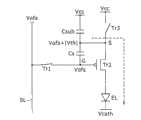
图2是示出包括在图1所示的显示装置中的像素2的具体配置和连接关系的电路图。如图2所示,像素2包括以有机EL装置等为代表的发光元件、取样晶体管Tr1、驱动晶体管Tr2、开关晶体管Tr3、保持电容Cs和辅助电容Csub。驱动晶体管Tr2是N沟道型的,具有作为栅极G的控制端子以及作为源极和漏极的一对电流端子。取样晶体管Tr1具有连接到第一扫描线WS的控制端子,还具有连接在信号线SL和驱动晶体管Tr2的栅极G之间的一对电流端子。如上所述,将作为视频信号的信号电位Vsig和预定参考电位Vofs从水平选择器供给信号线SL,以使得该信号电位Vsig与该参考电位Vofs交替。开关晶体管Tr3具有连接到第二扫描线DS的栅极,还具有一对电流端子,其中,该对电流端子中的一个连接到驱动晶体管Tr2的源极S,而该对电流端子中的另一个连接到电源线Vcc。注意,该电源线Vcc具有固定电压。保持电容Cs连接在驱动晶体管Tr2的栅极G和源极S之间。辅助电容Csub具有连接到固定电压Vcc的一个端子,还具有连接到保持电容Cs的另一端子。发光元件EL连接在驱动晶体管Tr2的漏极和接地线之间。换句话说,该二极管型发光元件EL具有连接到驱动晶体管Tr2的漏极的阳极,还具有连接到接地线的阴极。该接地线被供给预定的阴极电压Vcath。FIG. 2 is a circuit diagram showing a specific configuration and connection relationship of
在图2所示的像素2中,驱动晶体管Tr2是P沟道型的。其他晶体管(即,取样晶体管Tr1和开关晶体管Tr3)可以是P沟道型的,也可以是N沟道型的。在图的实施方式中,取样晶体管Tr1和开关晶体管Tr3都是P沟道型的,因此,形成该像素2的晶体管都是P沟道型的晶体管。In the
如上所述,驱动单元包括:写扫描器4,用于将控制信号顺序地供给第一扫描线WS;驱动扫描器5,用于将控制信号顺序地供给每条第二扫描线DS;以及水平选择器3,用于交替地将作为视频信号的信号电位Vsig和预定参考电位Vofs供给每条信号线SL。As described above, the drive unit includes: a
在这种配置中,当该信号线SL处于参考电位Vofs时该写扫描器4输出控制信号给第一扫描线WS以驱动该像素2,凭此执行校正驱动晶体管Tr2的阈值电压Vth的操作。进一步,当该信号线SL处于信号电位Vsig时该写扫描器4输出控制信号给该第一扫描线WS以驱动该像素2,凭此执行将该信号电位Vsig写到该保持电容Cs的写操作。在该信号电位Vsig被写到该保持电容Cs之后,该驱动扫描器5输出控制信号给第二扫描线DS以将电流传过该像素2,以便执行发光元件EL的发光操作。当该信号线SL处于该信号电位Vsig时,该写扫描器4输出控制信号到该第一扫描线WS来驱动该像素2,并且该写扫描器4同时执行校正该驱动晶体管Tr2的迁移率μ的变异的校正操作。In this configuration, the
图3是协助解释图2所示的像素2的操作的时序图。该时序图沿时间轴示出施加到各条扫描线WS和DS的控制信号的波形。为了简化符号,以下将用与对应的扫描线的附图标记相同的附图标记来表示控制信号。由于取样晶体管Tr1和开关晶体管Tr3都是P沟道型的,因此当扫描线WS和DS处于低电平时,取样晶体管Tr1和开关晶体管Tr3处于导通,而当扫描线WS和DS处于高电平时,取样晶体管Tr1和开关晶体管Tr3处于截止。该时序图连同各控制信号WS和DS的波形一起,示出驱动晶体管Tr2的栅极G的电位变化以及驱动晶体管Tr2的源极G的电位变化。该时序图还示出了施加到信号线SL的视频信号的波形。该视频信号具有使得信号电位Vsig与参考电位Vofs在一个水平期间(1H期间)内相互交替的波形。FIG. 3 is a timing chart of assistance in explaining the operation of the
在图3的时序图中,从时间T1至时间T9的期间被设置为一场的期间。在一场的该期间,顺序扫描像素阵列的每一行一次。该顺序图示出施加到一行中的像素的各条扫描线WS和DS的波形。In the timing chart of FIG. 3 , the period from time T1 to time T9 is set as a period of one field. During this period of one field, each row of the pixel array is scanned sequentially once. This sequence diagram shows the waveforms of the respective scan lines WS and DS applied to the pixels in one row.
在开始当前场的时间T1之前,取样晶体管Tr1处于截止状态,而开关晶体管Tr3处于导通状态。因此,驱动晶体管Tr2经由处于导通状态的开关晶体管Tr3连接到电源电压Vcc。由此,驱动晶体管Tr2一直根据预定输入电压Vgs将输出电流Ids供给发光元件EL。因此,在时间T1之前的阶段中,发光元件EL一直发光。此时施加到驱动晶体管Tr2的输入电压Vgs由栅极电位(G)和源极电位(S)之间的差表示。Before the time T1 when the current field starts, the sampling transistor Tr1 is in an off state, and the switching transistor Tr3 is in an on state. Therefore, the driving transistor Tr2 is connected to the power supply voltage Vcc via the switching transistor Tr3 in the on state. Thus, the driving transistor Tr2 always supplies the output current Ids to the light emitting element EL according to the predetermined input voltage Vgs. Therefore, in the period before time T1, the light emitting element EL keeps emitting light. The input voltage Vgs applied to the drive transistor Tr2 at this time is represented by the difference between the gate potential (G) and the source potential (S).
在开始当前场的时间T1,控制信号DS从低电平改变到高电平。从而,截止开关晶体管Tr3以将驱动晶体管Tr2与电源Vcc断开。因此,停止发光,并开始非发光期间。At time T1 when the current field starts, the control signal DS changes from low level to high level. Thus, the switching transistor Tr3 is turned off to disconnect the driving transistor Tr2 from the power supply Vcc. Therefore, light emission is stopped, and a non-light emission period starts.
在接下来的时间T2,控制信号DS再次变到低电平,以导通开关晶体管Tr3。从而将驱动晶体管Tr2的源极S升高到电源电位Vcc。驱动晶体管Tr2的栅极电位(G)也以与驱动晶体管Tr2的源极S的电位上高连锁的这种方式向上偏移(shift)到电源电位Vcc。At the next time T2, the control signal DS changes to low level again to turn on the switching transistor Tr3. The source S of the drive transistor Tr2 is thereby raised to the power supply potential Vcc. The gate potential (G) of the drive transistor Tr2 is also shifted upward to the power supply potential Vcc in such a manner that the potential of the source S of the drive transistor Tr2 is high in linkage.
此后,在信号线SL处于参考电位Vofs的时间T3上,控制信号WS变到低电平以导通取样晶体管Tr1。从而将参考电位Vofs写到驱动晶体管Tr2的栅极G。在这个阶段,驱动晶体管Tr2的输入电压Vgs为Vcc-Vofs,其高于阈值电压Vth足够多,因此,驱动晶体管Tr2被设置在导通状态。从时间T2到时间T3的期间为用于阈值电压校正的准备期间,在该期间,驱动晶体管Tr2的源极S和栅极G分别被复位到Vcc和Vofs。Thereafter, at time T3 when the signal line SL is at the reference potential Vofs, the control signal WS changes to low level to turn on the sampling transistor Tr1. The reference potential Vofs is thereby written to the gate G of the drive transistor Tr2. At this stage, the input voltage Vgs of the drive transistor Tr2 is Vcc-Vofs, which is sufficiently higher than the threshold voltage Vth, and therefore, the drive transistor Tr2 is set in the on state. The period from time T2 to time T3 is a preparation period for threshold voltage correction, during which the source S and gate G of the drive transistor Tr2 are reset to Vcc and Vofs, respectively.
之后,在时间T4,控制信号DS被设置在高电平,以截止开关晶体管Tr3。另一方面,取样晶体管Tr1保持在导通状态。在这种情况下,电流源中断,而驱动晶体管Tr2的栅极G保持固定在参考电位Vofs,以便源极S的电位降低。结果,在驱动晶体管Tr2截止的时间点,电流停止流动。当驱动晶体管Tr2截止时,与驱动晶体管Tr2的精确阈值电压Vth对应的电位差出现在源极S和栅极G之间。这个电位差被连接在驱动晶体管Tr2的源极S和栅极G之间的保持电容Cs保持。After that, at time T4, the control signal DS is set at a high level to turn off the switching transistor Tr3. On the other hand, the sampling transistor Tr1 is kept in an on state. In this case, the current source is interrupted, and the gate G of the drive transistor Tr2 is kept fixed at the reference potential Vofs, so that the potential of the source S is lowered. As a result, at the point of time when the drive transistor Tr2 is turned off, current stops flowing. When the driving transistor Tr2 is turned off, a potential difference corresponding to the precise threshold voltage Vth of the driving transistor Tr2 appears between the source S and the gate G. This potential difference is held by the hold capacitance Cs connected between the source S and the gate G of the drive transistor Tr2.
此后,在时间T5,控制信号WS被设置到高电平,以截止取样晶体管Tr1。驱动晶体管Tr2的栅极G与信号线SL断开,凭此结束阈值电压校正操作。因此,从时间T4到时间T5的期间为用于阈值电压校正操作的期间。Thereafter, at time T5, the control signal WS is set to high level to turn off the sampling transistor Tr1. The gate G of the drive transistor Tr2 is disconnected from the signal line SL, whereby the threshold voltage correction operation ends. Therefore, the period from time T4 to time T5 is a period for the threshold voltage correction operation.
在接下来的时间T6,控制信号WS被设置到低电平,以导通取样晶体管Tr1。此时,信号线SL处于信号电位Vsig。因此,信号电位Vsig被处于导通状态的取样晶体管Tr1取样,并且被写到驱动晶体管Tr2的栅极G。在接下来的时间T7,控制信号WS被设置到高电平,以截止取样晶体管Tr1,凭此结束将写信号电位Vsig的操作。即,在T6到T7的、取样晶体管Tr1处于导通的很短期间中,执行写信号电位Vsig到驱动晶体管Tr2的栅极G的信号电位写操作。从而驱动晶体管Tr2的输入电压Vgs变成Vth+Vsig。然而,当参考电位被设置在0V时获得这个所计算出来的值。At the next time T6, the control signal WS is set to low level to turn on the sampling transistor Tr1. At this time, the signal line SL is at the signal potential Vsig. Accordingly, the signal potential Vsig is sampled by the sampling transistor Tr1 in the on state, and written to the gate G of the driving transistor Tr2 . At the next time T7, the control signal WS is set to a high level to turn off the sampling transistor Tr1, thereby ending the operation to write the signal potential Vsig. That is, in a very short period from T6 to T7 in which the sampling transistor Tr1 is on, a signal potential writing operation of writing the signal potential Vsig to the gate G of the driving transistor Tr2 is performed. The input voltage Vgs of the drive transistor Tr2 thus becomes Vth+Vsig. However, this calculated value is obtained when the reference potential is set at 0V.
在信号电位写期间T6到T7中,同时进行关于驱动晶体管Tr2的迁移率μ的校正。在时序图中,用ΔV表示这种迁移率校正的量。即,在信号电位写期间T6到T7中,将信号电位Vsig写到驱动晶体管Tr2的栅极G,与此同时,将驱动晶体管Tr2的源极S的电位改变ΔV。因此,驱动晶体管Tr2的输入电压Vgs变成Vsig+Vth-ΔV,将是精确的。改变量ΔV精确地在消去驱动晶体管Tr2的迁移率μ的变异的方向起作用。具体来说,当驱动晶体管Tr2的迁移率μ相对高时,改变量ΔV大,输入电压Vgs相应地被压缩,因此迁移率μ的效应被抑制。另一方面,当驱动晶体管Tr2具有低迁移率μ时,改变量ΔV小,因此输入电压Vgs很少被压缩。因此,当迁移率μ低时,阻止了输入电压Vgs被非常大地压缩,因此迁移率μ的变异被均分(average)。In the signal potential writing period T6 to T7, correction regarding the mobility μ of the drive transistor Tr2 is simultaneously performed. In the timing diagram, the amount of this mobility correction is represented by ΔV. That is, in the signal potential writing period T6 to T7, the signal potential Vsig is written to the gate G of the drive transistor Tr2, and at the same time, the potential of the source S of the drive transistor Tr2 is changed by ΔV. Therefore, the input voltage Vgs of the drive transistor Tr2 becomes Vsig+Vth-ΔV, which will be accurate. The change amount ΔV acts precisely in the direction of canceling the variation in the mobility μ of the drive transistor Tr2. Specifically, when the mobility μ of the drive transistor Tr2 is relatively high, the amount of change ΔV is large, the input voltage Vgs is compressed accordingly, and thus the effect of the mobility μ is suppressed. On the other hand, when the driving transistor Tr2 has low mobility μ, the amount of change ΔV is small, so the input voltage Vgs is rarely compressed. Therefore, when the mobility μ is low, the input voltage Vgs is prevented from being compressed very much, so the variation in the mobility μ is averaged.
之后,在时间T8,控制信号DS被设置到低电平,以导通开关晶体管Tr3。由于驱动晶体管Tr2的源极S被连接到电源Vcc,所以电流开始流动,并且发光元件EL开始发光。此时,驱动晶体管Tr2的栅极G也由于自举效应而上升。由保持电容Cs保持栅极-源极电压Vgs维持值(Vsig+Vth-ΔV)。此时的漏极电流Ids和输入电压Vgs之间的关系通过在早先的晶体管特性等式1中用Vsig-ΔV+Vth替换Vgs给定如在下列等式2那样。After that, at time T8, the control signal DS is set to low level to turn on the switching transistor Tr3. Since the source S of the drive transistor Tr2 is connected to the power supply Vcc, current starts to flow, and the light emitting element EL starts to emit light. At this time, the gate G of the drive transistor Tr2 also rises due to the bootstrap effect. The gate-source voltage Vgs maintains a value (Vsig+Vth-ΔV) by the holding capacitor Cs. The relationship between the drain current Ids and the input voltage Vgs at this time is given by substituting Vsig-ΔV+Vth for Vgs in the earlier transistor
Ids=kμ(Vgs-Vth)2=kμ(Vsig-ΔV)2...等式2Ids=kμ(Vgs-Vth)2 =kμ(Vsig-ΔV)2 ...
在上述等式2中,k=(1/2)(W/L)Cox。这个特性等式2表明消去了阈值电压Vth的项,并且供给发光元件EL的输出电流Ids不依赖于驱动晶体管Tr2的阈值电压Vth。漏极电流Ids基本上由视频信号的信号电位Vsig确定。换句话说,发光元件EL以对应于信号电位Vsig的亮度发光。此时,该信号电位Vsig被校正改变量ΔV。校正量ΔV精确地用作消去定位于特性等式2的系数部分的迁移率μ的效应。因此,漏极电流Ids仅仅有效地依赖于信号电位Vsig。In
当到达最后时间T9时,将控制信号DS设置到高电平,以截止开关晶体管Tr3。从而,发光结束,并且完成当前场。之后,作出到下一场的过渡,以重复Vth校正操作、信号电位写与迁移率校正操作以及发光操作。When the final time T9 is reached, the control signal DS is set to high level to turn off the switching transistor Tr3. Thus, light emission ends, and the current field is completed. After that, a transition to the next field is made to repeat the Vth correction operation, the signal potential writing and mobility correction operation, and the light emitting operation.
接下来将参考图4至图7详细描述图2中所示的像素的操作。图4示出了在阈值校正准备期间T2至T4中像素电路的操作的状态。如图4所示,在准备期间T2至T4,取样晶体管Tr1和开关晶体管Tr3都处于导通。信号线SL处于参考电位Vofs。因此,在准备期间T2至T4中,电源电压Vcc被写到驱动晶体管Tr2的源极S,而参考电位Vofs被写到驱动晶体管Tr2的栅极G。驱动晶体管Tr2的输入电压Vgs因此而成为Vcc-Vofs。在这种情况下,将参考电压Vofs设置成满足Vcc-Vofs>|Vth|。Vth为驱动晶体管Tr2的阈值电压。在这个条件下,Vgs>|Vth|,因此驱动晶体管Tr2处于导通状态。在这种状态下,不必要的电流流向发光元件EL。为了防止出现这种情况,期望将准备期间T2至T4设置得尽量短,即,设置在几μs或更少。除此而外,期望设置参考电位Vofs的值仅仅稍微高于阈值电压Vth。Next, operations of the pixels shown in FIG. 2 will be described in detail with reference to FIGS. 4 to 7 . FIG. 4 shows the state of the operation of the pixel circuit in the threshold value correction preparation period T2 to T4. As shown in FIG. 4, during the preparation period T2 to T4, both the sampling transistor Tr1 and the switching transistor Tr3 are turned on. The signal line SL is at the reference potential Vofs. Therefore, in the preparation period T2 to T4, the power supply voltage Vcc is written to the source S of the drive transistor Tr2, and the reference potential Vofs is written to the gate G of the drive transistor Tr2. The input voltage Vgs of the drive transistor Tr2 thus becomes Vcc-Vofs. In this case, the reference voltage Vofs is set to satisfy Vcc-Vofs>|Vth|. Vth is the threshold voltage of the drive transistor Tr2. Under this condition, Vgs>|Vth|, so the drive transistor Tr2 is in an on state. In this state, unnecessary current flows to the light emitting element EL. In order to prevent this, it is desirable to set the preparation period T2 to T4 as short as possible, that is, to several μs or less. In addition to this, it is desirable to set the value of the reference potential Vofs only slightly higher than the threshold voltage Vth.
图5示出了在阈值校正期间T4至T5中像素的操作的状态。开关晶体管Tr3处于截止状态。作为结果,保存在保持电容Cs和辅助电容Csub中的电荷通过驱动晶体管Tr2放电到发光元件EL的阴极电位Vcath的一侧。驱动晶体管Tr2的源极电位在该放电过程中下降。在驱动晶体管Tr2的源极电位达到Vofs+|Vth|的时间点,驱动晶体管Tr2截止。从而,连接在驱动晶体管Tr2的栅极G和源极S之间的保持电容Cs保持驱动晶体管Tr2的阈值电压|Vth|。在这样执行阈值电压校正操作之后,取样晶体管Tr1被截止。FIG. 5 shows the states of the operation of the pixels in the threshold correction period T4 to T5. The switching transistor Tr3 is in an off state. As a result, the charges stored in the storage capacitor Cs and the auxiliary capacitor Csub are discharged to the side of the cathode potential Vcath of the light emitting element EL through the drive transistor Tr2. The source potential of the drive transistor Tr2 drops during this discharge. At the point of time when the source potential of the drive transistor Tr2 reaches Vofs+|Vth|, the drive transistor Tr2 is turned off. Thus, the holding capacitance Cs connected between the gate G and the source S of the driving transistor Tr2 holds the threshold voltage |Vth| of the driving transistor Tr2. After the threshold voltage correction operation is thus performed, the sampling transistor Tr1 is turned off.
图6示出在信号写与迁移率校正期间T6至T7中像素的操作的状态。在该状态下,信号线SL从参考电位Vofs改变到信号电位Vsig。取样晶体管Tr1再次被导通。从而,将信号电位Vsig写到驱动晶体管Tr2的栅极G。另一方面,由保持电容Cs与辅助电容Csub之间的电容比确定的耦合(coupling)进入在驱动晶体管Tr2的源极S处的电位。从而,驱动晶体管Tr2的输入电压Vgs具有由下列等式3表达的值。FIG. 6 shows states of operation of pixels in signal writing and mobility correction periods T6 to T7. In this state, the signal line SL changes from the reference potential Vofs to the signal potential Vsig. The sampling transistor Tr1 is turned on again. Thus, the signal potential Vsig is written to the gate G of the drive transistor Tr2. On the other hand, coupling determined by the capacitance ratio between the storage capacitance Cs and the auxiliary capacitance Csub enters the potential at the source S of the drive transistor Tr2. Thus, the input voltage Vgs of the drive transistor Tr2 has a value expressed by
在这种状态下,如虚线所示,电流流过驱动晶体管Tr2。因此源极S的电位改变ΔV,以便进行迁移率校正。即,信号写与迁移率校正期间T6至T7限定迁移率校正时间t。迁移率校正时间t为几μs的值那么短。迁移率校正之后的电流值Ids由下列等式4表达。In this state, current flows through the drive transistor Tr2 as indicated by a dotted line. The potential of the source S is therefore changed by ΔV for mobility correction. That is, the signal writing and mobility correction periods T6 to T7 define the mobility correction time t. The mobility correction time t is as short as a value of several μs. The current value Ids after mobility correction is expressed by
(其中
图7示出在发光期间T8至T9中像素电路的操作的状态。在该发光期间中,取样晶体管Tr1处于截止,而开关晶体管Tr3处于导通。因此稳态电流从电源电位Vcc通过开关晶体管Tr3和驱动晶体管Tr流向发光元件EL的阴极电位Vcath,以便执行发光操作。此时流动的该稳态电流(驱动电流Ids)受驱动晶体管Tr2的输入电压Vgs控制。如上所述,已经针对阈值电压Vth和迁移率μ变异对输入电压Vgs进行了校正,以便可以获得高一致性图像质量,而没有亮度差异。附带地,在发光期间中,驱动晶体管Tr2的源极电位上升到电源电位Vcc,而驱动晶体管Tr2的栅极电位也以与驱动晶体管Tr2的源极电位连锁的方式上升。FIG. 7 shows the state of the operation of the pixel circuit in the light emitting periods T8 to T9. During this light emission period, the sampling transistor Tr1 is turned off, and the switching transistor Tr3 is turned on. A steady-state current therefore flows from the power supply potential Vcc to the cathode potential Vcath of the light emitting element EL through the switching transistor Tr3 and the drive transistor Tr, so that a light emitting operation is performed. This steady-state current (drive current Ids) flowing at this time is controlled by the input voltage Vgs of the drive transistor Tr2. As described above, the input voltage Vgs has been corrected for threshold voltage Vth and mobility μ variation so that high uniform image quality can be obtained without luminance difference. Incidentally, during the light emitting period, the source potential of the drive transistor Tr2 rises to the power supply potential Vcc, and the gate potential of the drive transistor Tr2 also rises in linkage with the source potential of the drive transistor Tr2 .
如从上述描述清楚地那样,在使用P沟道型驱动晶体管并且开关晶体管Tr3被添加到的、根据本发明的第一实施方式的像素电路中,可以固定供给每个像素的电源电位Vcc。这消除了对电源脉冲的需要,以及对大输出缓冲器尺寸的需要。因此而可以保障其面积占据面板的屏幕有宽广的布局面积,并且获得更长的寿命。除此而外,通常,没有LDD区域的P沟道型驱动晶体管的特性的变异小于P沟道型驱动晶体管的特性的变异,这是熟知的。因此,在本发明中,通过选择P沟道型的驱动晶体管Tr2,可以抑制驱动晶体管Tr2的特性的变异,并且容易被校正。除此而外,在本发明中,施加到驱动晶体管Tr2的电压的幅度最大为大约Vcc-Vcath。这个电压Vcc-Vcath为大约10V。因此,例如,可以保障对驱动晶体管Tr2的耐压(withstand voltage)有足够的余地,并且减少栅极绝缘膜的厚度。As is clear from the above description, in the pixel circuit according to the first embodiment of the present invention using the P-channel type drive transistor and to which the switching transistor Tr3 is added, the power supply potential Vcc supplied to each pixel can be fixed. This eliminates the need for power pulses, and the need for large output buffer sizes. Therefore, the screen whose area occupies the panel can be guaranteed to have a wide layout area and obtain a longer lifespan. In addition, generally, the variation in the characteristics of the P-channel type driving transistor without the LDD region is smaller than the variation in the characteristics of the P-channel type driving transistor, which is well known. Therefore, in the present invention, by selecting the drive transistor Tr2 of the P-channel type, variations in the characteristics of the drive transistor Tr2 can be suppressed and easily corrected. Besides, in the present invention, the magnitude of the voltage applied to the drive transistor Tr2 is approximately Vcc-Vcath at the most. This voltage Vcc-Vcath is about 10V. Therefore, for example, it is possible to secure a sufficient margin for the withstand voltage of the drive transistor Tr2 and reduce the thickness of the gate insulating film.
接下来将描述本发明的第二实施方式的显示装置。该实施方式可以可变地自动根据信号电位的电平来调整迁移率校正时间t。图8是示出信号电位与最佳迁移率校正时间之间的关系的图形。纵坐标轴指示信号电位,而横坐标轴指示最佳迁移率校正时间。在驱动晶体管Tr2是如本发明中的那样的P沟道型的晶体管的情况下,随着信号电位变低,驱动电流增加并且发光亮度升高。因此,随着信号电位向上偏移,发光亮度从白电平通过灰度电平改变到黑电平。从该图形清楚的那样,当信号电位处于白电平时,最佳迁移率校正时间趋向于相当短,而当信号电位处于黑电平时,相反地趋向于长。为了提供屏幕的一致性并增强图像质量,希望自适应地根据信号电位控制迁移率校正时间。Next, a display device of a second embodiment of the present invention will be described. This embodiment can variably and automatically adjust the mobility correction time t according to the level of the signal potential. FIG. 8 is a graph showing the relationship between signal potential and optimum mobility correction time. The axis of ordinate indicates the signal potential, and the axis of abscissa indicates the optimum mobility correction time. In the case where the drive transistor Tr2 is a P-channel type transistor as in the present invention, as the signal potential becomes lower, the drive current increases and the light emission luminance increases. Therefore, as the signal potential shifts upward, the light emission luminance changes from the white level through the gray level to the black level. As is clear from this graph, the optimum mobility correction time tends to be relatively short when the signal potential is at the white level, and conversely tends to be long when the signal potential is at the black level. In order to provide screen uniformity and enhance image quality, it is desirable to adaptively control the mobility correction time according to the signal potential.
图9是协助解释根据本发明的第二实施方式的显示装置的操作的时序图。为了便于理解,用相同附图标记标识与图3中的第一实施方式的时序图对应的部件。该第二实施方式在如下的方面不同于第一实施方式:限定信号写与迁移率校正期间的控制信号WS的负极性脉冲的上升沿被变钝(blunt)。从而,迁移率校正时间t可以自动根据信号电位Vsig的电平可变地调整。FIG. 9 is a timing chart of assistance in explaining the operation of the display device according to the second embodiment of the present invention. For ease of understanding, components corresponding to the timing chart of the first embodiment in FIG. 3 are identified with the same reference numerals. This second embodiment differs from the first embodiment in that the rising edge of the negative polarity pulse of the control signal WS defining the signal writing and mobility correction period is blunt. Thus, the mobility correction time t can be automatically and variably adjusted in accordance with the level of the signal potential Vsig.
图10是以放大的尺度示出出现在图9所示的时间T6至时间T7的期间中的控制信号WS的负极性脉冲的波形图。取样晶体管Tr1是P沟道型的。取样晶体管Tr1通过将控制信号WS从高电平改变到低电平来导通,相反,通过将控制信号WS从低电平改变到高电平来截止。从高电平改变到低电平的下降沿很陡峭,以便取样晶体管Tr1被立即导通。另一方面,从低电平到高电平的改变期间的上升沿波形被变钝,并且截止时间(off timing)根据操作点而不同。将信号电位Vsig施加到取样晶体管Tr1的源极侧(source side),并且将控制信号WS施加到取样晶体管Tr1的栅极侧(gate side)。取样晶体管Tr1的操作点根据信号电位Vsig而不同。在信号电位Vsig很低的白层次(white gradation)处,操作点也很低,因此取样晶体管Tr1被截止的相对早。因此,在白层次处的迁移率校正时间相对短。另一方面,当信号电位Vsig处于黑层次(black gradation)时,操作点接近高电平。因此,取样晶体管Tr1被截止的时间向后偏移,而黑层次处的迁移率校正时间延长。介于白层次和黑层次之间的灰度层次处的迁移率校正时间也介于其间。因此,本实施方式可以自动根据信号电位Vsig的电平最佳地调整迁移率校正时间。对于这样的迁移率校正,希望取样晶体管Tr1是P沟道型而不是N沟道型的晶体管。FIG. 10 is a waveform diagram showing a negative polarity pulse of the control signal WS appearing in the period from time T6 to time T7 shown in FIG. 9 on an enlarged scale. The sampling transistor Tr1 is of a P-channel type. The sampling transistor Tr1 is turned on by changing the control signal WS from high level to low level, and conversely, is turned off by changing the control signal WS from low level to high level. The falling edge changing from high level to low level is steep so that the sampling transistor Tr1 is turned on immediately. On the other hand, a rising edge waveform during a change from low level to high level is blunted, and off timing differs depending on the operating point. The signal potential Vsig is applied to the source side (source side) of the sampling transistor Tr1, and the control signal WS is applied to the gate side (gate side) of the sampling transistor Tr1. The operating point of the sampling transistor Tr1 differs according to the signal potential Vsig. At a white gradation where the signal potential Vsig is very low, the operating point is also low, so the sampling transistor Tr1 is turned off relatively early. Therefore, the mobility correction time at the white level is relatively short. On the other hand, when the signal potential Vsig is at black gradation, the operating point is close to a high level. Therefore, the timing at which the sampling transistor Tr1 is turned off is shifted backward, and the mobility correction time at the black level is extended. The mobility correction time at the gray level between the white level and the black level is also in between. Therefore, the present embodiment can automatically and optimally adjust the mobility correction time according to the level of the signal potential Vsig. For such mobility correction, it is desirable that the sampling transistor Tr1 is a P-channel type transistor rather than an N-channel type transistor.
图11是示出用于该第二实施方式的写扫描器的实施方式的电路图。图11示意性地示出了写扫描器4的输出部分的三个级(stage)以及连接到写扫描器4的像素阵列单元1的三个行(三条线)。写扫描器4由移位寄存器S/R形成。写扫描器4根据外部输入的时钟信号操作,以顺序地类似地发送外部输入的开始信号,从而在每个级顺序输出信号。NAND元件连接到移位寄存器S/R的各个级。NAND元件使从相邻级的移位寄存器S/R输出的顺序信号经历NAND处理,从而产生担当控制信号的基的矩形波形。该矩形波形经由反相器(inverter)输入到输出缓冲器。该输出缓冲器根据从移位寄存器S/R侧供给输入信号操作,以将最终的控制信号供给像素阵列单元1的对应扫描线WS。FIG. 11 is a circuit diagram showing an embodiment of a write scanner used in this second embodiment. FIG. 11 schematically shows three stages of the output section of the
该输出缓冲器由在电源电位Vcc与地电位Vss之间相互串联的一对开关元件形成。一个开关元件是P沟道型晶体管TrP,而另一个是N沟道型晶体管TrN。附带地,在等效电路中,连接到各个缓冲器的像素阵列单元1侧的线由电阻元件R和电容元件C表示。在这种情况下,脉冲电源7连接到每一级中的输出缓冲器的接地线Vss。该脉冲电源7以1H周期输出电源脉冲,并将该电源脉冲供给接地线Vss。输出缓冲器根据从NAND元件侧供给的输入脉冲提取电源脉冲,并将该电源脉冲作为输出脉冲供给扫描线WS侧。如图11的下部所示,负极性的阴影部分的电源脉冲具有很陡峭的下降沿和缓慢的上升沿。将上升沿的缓慢部分照其原样提取出来,以便用作针对迁移率校正时间的自动控制的控制信号WS。The output buffer is formed by a pair of switching elements connected in series between a power supply potential Vcc and a ground potential Vss. One switching element is a P-channel type transistor TrP, and the other is an N-channel type transistor TrN. Incidentally, in the equivalent circuit, lines connected to the
图12是协助解释图11所示的写扫描器的操作的时序图。如图12所示,在每一1H期间,脉冲电源7都输出包括负极性脉冲P的电源脉冲串到输出缓冲器的接地线。图12的时序图还示出其时序与电源脉冲的时序一致的、输出缓冲器的输入脉冲和输出脉冲。图12示出供给第(N-1)级和第N级的输出缓冲器的输入脉冲和输出脉冲。在每级中,输入脉冲是偏移一H的矩形脉冲。当输入脉冲被施加到第(N-1)级的输出缓冲器时,导通反相器来从接地线照原样提取脉冲P。该脉冲P成为第(N-1)级的输出缓冲器的输出脉冲,然后被照原样输出到相应的第(N-1)扫描线WS。类似地,当输入脉冲被施加到第N级的输出缓冲器时,将输出脉冲从第N级的输出缓冲器输出到相应的扫描线WS。FIG. 12 is a timing chart of assistance in explaining the operation of the write scanner shown in FIG. 11 . As shown in FIG. 12 , in every 1H period, the
作为参考,以下将描述电源线不固定在电源电位Vcc而是被供给脉冲的显示装置的示例。图13是示出根据本参考示例的显示装置的一般配置的框图。如图13所示,该显示装置包括像素阵列单元1和用于驱动该像素阵列单元1的驱动单元。像素阵列单元1包括具有行形式的扫描线WS、具有列形式的信号线SL、具有矩阵形式的像素2以及与像素2的每行相对应地排列的馈送器线(电源线)VL,其中,在该矩阵形式中像素布置在扫描线WS与信号线SL相互交叉的部分上。附带地,在本示例中,将三RGB原色之一分配给每个像素2,依此允许彩色显示。然而,显示装置不限于此,也包括单色显示装置。该驱动单元包括:写扫描器4,用于通过顺序将控制信号供给各条扫描线WS来以行为单位执行像素2的行顺序驱动;电源扫描器6,用于根据行顺序驱动,将在第一电位和第二电位之间变化的电源电压供给每条馈送器线;以及信号选择器(水平选择器)3,用于根据行顺序驱动,将作为驱动信号的信号电位以及参考电位供给具有列形式的信号线SL。For reference, an example of a display device in which a power supply line is not fixed at the power supply potential Vcc but supplied with pulses will be described below. FIG. 13 is a block diagram showing a general configuration of a display device according to this reference example. As shown in FIG. 13 , the display device includes a
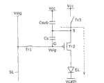
图14是示出包括在根据图13所示的参考示例的显示装置中的像素2的具体配置和连接关系的电路图。如图13所示,像素2包括以有机EL装置等为代表的发光元件、取样晶体管Tr1、驱动晶体管Tr2和保持电容Cs。取样晶体管Tr1的控制端子(栅极)连接到相应的扫描线WS,取样晶体管Tr1的一对电流端子(源极和漏极)之一连接到相应信号线SL,而取样晶体管Tr1的该对电流端子中的另一个连接到驱动晶体管Tr2的控制端子(栅极G)。驱动晶体管Tr2的一对电流端子(源极S和漏极G)之一连接到发光元件EL,而驱动晶体管Tr2的该对电流端子中的另一个连接到相应馈送器线VL。在本示例中,驱动晶体管Tr2是N沟道型的。驱动晶体管Tr2的漏极连接到馈送器线VL,而驱动晶体管Tr2的源极S作为输出节点连接到发光元件EL的阳极。发光元件EL的阴极连接到预定阴极电压Vcath。保持电容Cs连接在作为驱动晶体管Tr2的一个电流端子的源极S和作为驱动晶体管Tr2的控制端子的栅极G之间。FIG. 14 is a circuit diagram showing a specific configuration and connection relationship of
在这样的配置中,取样晶体管Tr1根据从扫描线WS供给的控制信号引导(conduct)对从信号线SL供给的信号电位取样,并将该信号电位保持在保持电容Cs中。驱动晶体管Tr2被从馈送线VL以第一电位(高电位Vdd)供给电流,并根据保持在保持电容Cs中的信号电位将驱动电流传过发光元件EL。为了在信号线SL处于信号电位的时间期间中将取样晶体管Tr1设置在引导状态中,写扫描器4输出预定脉冲宽度的控制信号到扫描线WS,凭此将信号电位保持在保持电容Cs中,并且同时对信号电位进行关于驱动晶体管Tr2的迁移率μ的校正。此后,驱动晶体管Tr2根据写到保持电容Cs的信号电位Vsig,向发光元件EL供给驱动电流。由此开始发光操作。In such a configuration, the sampling transistor Tr1 conducts sampling of the signal potential supplied from the signal line SL in accordance with the control signal supplied from the scanning line WS, and holds the signal potential in the holding capacitor Cs. The driving transistor Tr2 is supplied with a current at a first potential (high potential Vdd) from the feed line VL, and passes a driving current through the light emitting element EL according to the signal potential held in the holding capacitor Cs. In order to set the sampling transistor Tr1 in the pilot state during the time period when the signal line SL is at the signal potential, the
该像素2具有阈值电压校正功能以及上述迁移率校正功能。具体来说,在取样晶体管Tr1取样信号电位Vsig之前的第一时间,电源扫描器6将馈送器线VL从第一电位(高电位Vdd)改变到第二电位(低电位Vss2)。此外,写扫描器4在取样晶体管Tr1取样信号电位Vsig之前的第二时间,使得取样晶体管Tr1引导将来自信号线SL的参考电位Vss1施加到驱动晶体管Tr2的栅极G,并且驱动晶体管Tr2的源极S被设置到第二电位(Vss2)。在该第二时间之后的第三时间,电源扫描器6将馈送器线VL从第二电位Vss2改变到第一电位Vdd,以将与驱动晶体管Tr2的阈值电压Vth相应的电压保持在保持电容Cs。通过这样的阈值电压校正功能,显示装置可以消去驱动晶体管Tr2的阈值电压Vth在每个像素中变化的影响。This
该像素2还具有自举功能(bootstrap function)。具体来说,写扫描器4在信号电位Vsig被保持在保持电容Cs中的阶段,取消控制信号向扫描线WS的施加,以便将取样晶体管Tr1设置在非引导状态,来将驱动晶体管Tr2的栅极G与信号线SL电断开。从而,驱动晶体管Tr2的栅极G的电位与驱动晶体管Tr2的源极的电位的变化互锁(interlock),因此栅极G与源极S之间的电压Vgs可以保持恒定。The
图15是协助解释根据示出在图14中的像素2的操作的时序图。图15沿公共时间轴示出了扫描线WS的电位的变化、馈送器线VL的电位的变化以及信号线SL的电位的变化。也与这些电位变化平行地示出了驱动晶体管的栅极G和源极S的电位的变化。FIG. 15 is a timing chart of assistance in explaining the operation according to the
用于导通取样晶体管Tr1的控制信号脉冲被施加到扫描线WS。根据像素阵列单元的行顺序驱动,以一场(1f)的周期(cycle of one field(1f))将这种控制信号脉冲施加到扫描线WS。在一个水平扫描期间(1H),这种控制信号脉冲包括两个脉冲。之后,在本说明书中,头一脉冲可以称为第一脉冲P1,随后的脉冲可以成为第二脉冲P2。在一场(1f)的同一周期中,馈送器线VL在高电位Vdd和低电位Vss2之间改变。在一个水平扫描期间(1H)内,向信号线SL供给在信号电位Vsig和参考电位Vss1之间改变的驱动信号。A control signal pulse for turning on the sampling transistor Tr1 is applied to the scanning line WS. This control signal pulse is applied to the scan line WS in a cycle of one field (1f) according to the row-sequential driving of the pixel array unit. During one horizontal scanning period (1H), this control signal pulse consists of two pulses. Hereinafter, in this specification, the first pulse may be referred to as a first pulse P1, and subsequent pulses may be referred to as a second pulse P2. During the same period of one field (1f), the feeder line VL changes between a high potential Vdd and a low potential Vss2. During one horizontal scanning period (1H), a drive signal changing between the signal potential Vsig and the reference potential Vss1 is supplied to the signal line SL.
如图15的时序图所示,该像素从之前场的发光期间进入当前场(field inquestion)的非发光期间(non-emission period),此后开始当前场的发光期间。在非发光期间,执行准备操作、阈值电压校正操作、信号写操作、迁移率校正操作等等。As shown in the timing diagram of FIG. 15, the pixel enters the non-emission period (non-emission period) of the current field (field inquiry) from the light emission period of the previous field, and then starts the light emission period of the current field. During the non-emission period, a preparation operation, a threshold voltage correction operation, a signal writing operation, a mobility correction operation, and the like are performed.
在之前场的发光期间,馈送器线VL处于高电位Vdd,并且驱动晶体管Tr2将驱动电流Ids供给发光元件EL。驱动电流Ids经由驱动晶体管Tr2从馈送器线VL传送通过发光元件EL,然后流入阴极线。During the light emission period of the previous field, the feeder line VL is at the high potential Vdd, and the drive transistor Tr2 supplies the drive current Ids to the light emitting element EL. The drive current Ids is transmitted from the feeder line VL through the light emitting element EL via the drive transistor Tr2, and then flows into the cathode line.
接下来,当开始当前场的非发光期间时,馈送器线VL在第一时间T1从高电位Vdd改变到低电位Vss2。从而,馈送器线VL被放电到低电位Vss2,并且驱动晶体管Tr2的源极S的电位降到低电位Vss2。由此而将发光元件EL的阳极电位(即,驱动晶体管Tr2的源极电位)设置在反偏压状态(reverse biasstate),以便驱动电流停止流动并且发光元件EL截止。驱动晶体管的栅极G的电位也以与驱动晶体管的源极S的电位下降互锁的方式下降。Next, when the non-emission period of the current field starts, the feeder line VL changes from the high potential Vdd to the low potential Vss2 at the first time T1. Thereby, the feeder line VL is discharged to the low potential Vss2, and the potential of the source S of the drive transistor Tr2 falls to the low potential Vss2. Thereby, the anode potential of the light emitting element EL (ie, the source potential of the driving transistor Tr2 ) is set in a reverse bias state, so that the driving current stops flowing and the light emitting element EL is turned off. The potential of the gate G of the drive transistor also drops in interlock with the drop in potential of the source S of the drive transistor.
在接下来的时间T2,扫描线WS从低电平改变到高电平,从而将取样晶体管Tr1设置在引导状态(conducting state)。此时,信号线SL处于参考电位Vss1。因此,驱动晶体管Tr2的栅极G的电位通过引导取样晶体管Tr1而变成信号线SL的参考电位Vss1。此时的驱动晶体管Tr2的源极S的电位是电位Vss2,其比参考电位Vss1低得多。由此而初始化驱动晶体管Tr2的栅极G与源极S之间的电压Vgs,以使得其比驱动晶体管Tr2的阈值电压Vth更大。从时间T1到时间T3的期间T1到T3是用于事先设置驱动晶体管Tr2的栅极G与源极S之间的电压Vgs等于或大于阈值电压Vth的准备期间。At the next time T2, the scanning line WS changes from low level to high level, thereby setting the sampling transistor Tr1 in a conducting state. At this time, the signal line SL is at the reference potential Vss1. Therefore, the potential of the gate G of the driving transistor Tr2 becomes the reference potential Vss1 of the signal line SL by leading the sampling transistor Tr1 . The potential of the source S of the driving transistor Tr2 at this time is a potential Vss2 which is much lower than the reference potential Vss1. Thereby, the voltage Vgs between the gate G and the source S of the drive transistor Tr2 is initialized so as to be larger than the threshold voltage Vth of the drive transistor Tr2 . The period T1 to T3 from the time T1 to the time T3 is a preparation period for setting the voltage Vgs between the gate G and the source S of the drive transistor Tr2 to be equal to or greater than the threshold voltage Vth in advance.
此后,在时间T3,馈送器线VL从低电位Vss2转变到高电位Vdd,而驱动晶体管Tr2的源极S的电位开始上升。不久,当驱动晶体管Tr2的栅极G与源极S之间的电压Vgs变成阈值电压Vth时切断电流。因此,与驱动晶体管Tr2的阈值电压Vth相应的电压被写入保持电容Cs。这就是阈值电压校正操作。此时,为了电流仅仅流到保持电容Cs侧而不流过发光元件EL,将阴极电位Vcath设置成使得发光元件EL截止。Thereafter, at time T3, the feeder line VL transitions from the low potential Vss2 to the high potential Vdd, and the potential of the source S of the drive transistor Tr2 starts to rise. Soon, the current is cut off when the voltage Vgs between the gate G and the source S of the drive transistor Tr2 becomes the threshold voltage Vth. Therefore, a voltage corresponding to the threshold voltage Vth of the drive transistor Tr2 is written into the storage capacitor Cs. This is the threshold voltage correction operation. At this time, in order for the current to flow only to the holding capacitor Cs side and not to flow through the light emitting element EL, the cathode potential Vcath is set so that the light emitting element EL is turned off.
在时间T4,扫描线WS从高电平返回低电平。换句话说,消除了施加到扫描线WS的第一脉冲P1,以便将取样晶体管设置在截止状态。像从上述描述清楚地看出的那样,施加第一脉冲P1到取样晶体管Tr1的栅极来执行阈值电压校正操作。At time T4, the scan line WS returns from high level to low level. In other words, the first pulse P1 applied to the scan line WS is eliminated to set the sampling transistor in an off state. As is clear from the above description, the threshold voltage correction operation is performed by applying the first pulse P1 to the gate of the sampling transistor Tr1.
此后,信号线SL从参考电位Vss1改变到信号电位Vsig。接下来,在时间T5,扫描线WS再次从低电平上升到高电平。换句话说,将第二脉冲P2施加到取样晶体管Tr1的栅极。从而,再次导通取样晶体管Tr1来对来自信号线SL的信号电位取样。驱动晶体管Tr2的栅极G的电位因此成为信号电位Vsig。在这种情况下,因为发光元件EL首先处于截止状态(高阻抗状态),所以流过驱动晶体管Tr2的漏极和源极之间的电流完全流入到保持电容Cs和发光元件EL的等效电容,并开始充电。此后,在取样晶体管Tr1被截止的时间T6之前,驱动晶体管Tr2的源极S的电位上升ΔV。因此,将视频信号的信号电位Vsig以被添加到阈值电压Vth的形式写入保持电容Cs,并且将用于迁移率校正的电压ΔV从保持在保持电容Cs中的电压中减去。因此,从时间T5到时间T6的期间T5至T6是信号写期间和迁移率校正期间。换句话说,当将第二脉冲P2施加到扫描线WS时,执行信号写操作和迁移率校正操作。信号写期间和迁移率校正期间T5至T6等于第二脉冲P2的脉冲宽度。即,第二脉冲P2的脉冲宽度限定迁移率校正期间。Thereafter, the signal line SL changes from the reference potential Vss1 to the signal potential Vsig. Next, at time T5, the scanning line WS rises from low level to high level again. In other words, the second pulse P2 is applied to the gate of the sampling transistor Tr1. Thus, the sampling transistor Tr1 is turned on again to sample the signal potential from the signal line SL. The potential of the gate G of the drive transistor Tr2 thus becomes the signal potential Vsig. In this case, since the light emitting element EL is in an off state (high impedance state) first, the current flowing between the drain and the source of the driving transistor Tr2 completely flows into the holding capacitance Cs and the equivalent capacitance of the light emitting element EL , and start charging. Thereafter, until the time T6 when the sampling transistor Tr1 is turned off, the potential of the source S of the driving transistor Tr2 rises by ΔV. Therefore, the signal potential Vsig of the video signal is written in the holding capacity Cs in a form added to the threshold voltage Vth, and the voltage ΔV for mobility correction is subtracted from the voltage held in the holding capacity Cs. Therefore, the period T5 to T6 from the time T5 to the time T6 is a signal writing period and a mobility correction period. In other words, when the second pulse P2 is applied to the scan line WS, a signal write operation and a mobility correction operation are performed. The signal writing period and the mobility correction period T5 to T6 are equal to the pulse width of the second pulse P2. That is, the pulse width of the second pulse P2 defines the mobility correction period.
因此,在信号写期间T5至T6同时执行信号电位Vsig的写和校正量ΔV的调整。信号电位Vsig越高,则驱动晶体管Tr2供给的电流Ids就越大,并且校正量ΔV的绝对值就越高。因此,根据发光亮度的级别来进行迁移率校正。当固定信号电位Vsig时,驱动晶体管Tr2的迁移率μ越高,则校正量ΔV的绝对值越高。换句话说,迁移率μ越高,则对保持电容Cs的负反馈量ΔV越大。因此,可以消除每个像素的迁移率μ的变异。Therefore, writing of the signal potential Vsig and adjustment of the correction amount ΔV are simultaneously performed during the signal writing period T5 to T6. The higher the signal potential Vsig is, the larger the current Ids supplied by the drive transistor Tr2 is, and the higher the absolute value of the correction amount ΔV is. Therefore, mobility correction is performed according to the level of emission luminance. When the signal potential Vsig is fixed, the higher the mobility μ of the drive transistor Tr2 is, the higher the absolute value of the correction amount ΔV is. In other words, the higher the mobility μ, the larger the negative feedback amount ΔV to the storage capacitance Cs. Therefore, variation in the mobility μ for each pixel can be eliminated.
最后,在时间T6,如上所述,扫描线WS改变到低电平侧,以将取样晶体管Tr1设置在截止状态。从而,驱动晶体管Tr2的栅极G与信号线SL断开。与此同时,漏极电流Ids开始流过发光元件EL。从而,发光元件EL的阳极电位根据驱动电流Ids上升。发光元件EL的阳极电位的上升正是驱动晶体管Tr2的源极S的电位的上升。当驱动晶体管Tr2的源极S的电位上升时,由于保持电容Cs的自举操作的缘故,驱动晶体管Tr2的栅极G的电位也以与驱动晶体管Tr2的源极S的电位互锁的方式上升。栅极电位的上升量等于源极电位的上升量。因此在发光期间,驱动晶体管Tr2的栅极G与源极S之间的电压Vgs保持为恒定。栅极电压Vgs的值为关于阈值电压Vth和迁移率μ校正信号电位Vsig的结果。驱动晶体管Tr2运行在饱和区。即,驱动晶体管Tr2供给与栅极-源极电压Vgs相应的驱动电流Ids。电压Vgs的值为关于阈值电压Vth和迁移率μ校正信号电位Vsig的结果。Finally, at time T6, as described above, the scanning line WS is changed to the low level side to set the sampling transistor Tr1 in an off state. Thus, the gate G of the drive transistor Tr2 is disconnected from the signal line SL. At the same time, the drain current Ids starts to flow through the light emitting element EL. Accordingly, the anode potential of the light emitting element EL rises according to the driving current Ids. The rise in the potential of the anode of the light emitting element EL is exactly the rise in the potential of the source S of the drive transistor Tr2. When the potential of the source S of the drive transistor Tr2 rises, the potential of the gate G of the drive transistor Tr2 also rises in an interlocked manner with the potential of the source S of the drive transistor Tr2 due to the bootstrap operation of the storage capacitor Cs. . The rising amount of the gate potential is equal to the rising amount of the source potential. During light emission, therefore, the voltage Vgs between the gate G and source S of the drive transistor Tr2 is kept constant. The value of the gate voltage Vgs is a result of correcting the signal potential Vsig with respect to the threshold voltage Vth and the mobility μ. The driving transistor Tr2 operates in a saturation region. That is, the drive transistor Tr2 supplies a drive current Ids corresponding to the gate-source voltage Vgs. The value of the voltage Vgs is a result of correcting the signal potential Vsig with respect to the threshold voltage Vth and the mobility μ.
图16是以放大的尺寸示出根据图13和图14所示的参考示例的显示装置的电源扫描器6的示意图。如图16所示,在每一级中,电源扫描器6具有由反相器形成的输出缓冲器。该输出缓冲器输出电源脉冲到相应的馈送器线VL。如上所述,根据参考示例的显示装置向电源线供给脉冲。将该脉冲作为电源脉冲从电源扫描器6供给像素2侧。在发光的时候,面板电源处于高电位Vdd,因此电源扫描器6的最后级中的缓冲器的P沟道晶体管被导通,以便将电源电压供给像素侧。一个像素的发光电流为几μA。由于每线(每行)大约有1000个像素沿水平方向相互连接,所以总输出电流为几mA。为了防止在使得驱动电流流动时的电压降,需要配置几mm的大尺寸输出缓冲器,因此导致很大的布局面积。此外,由于发光电流一直不断地流,所以输出缓冲器的晶体管的特性急剧恶化,从而不可能获得长期使用的可靠性。FIG. 16 is a schematic diagram showing the
如图17所示,根据本发明的实施方式的显示装置具有薄膜装置结构。该图示意性地示出了形成在绝缘衬底上的像素的截面结构。如图17所示,像素包括包含多个薄膜晶体管的晶体管部分(在图中图示了一个TFT)、保持电容等的电容部分以及有机EL元件等的发光部分。通过TFT工艺将晶体管部分和电容部分形成在衬底上,并且将有机EL元件等的发光部分堆叠在晶体管部分和电容部分上。通过粘合剂将透明背衬附着在发光部分来形成平板。As shown in FIG. 17, a display device according to an embodiment of the present invention has a thin film device structure. The figure schematically shows a cross-sectional structure of a pixel formed on an insulating substrate. As shown in FIG. 17 , a pixel includes a transistor portion including a plurality of thin film transistors (one TFT is shown in the figure), a capacitor portion such as a storage capacitor, and a light emitting portion such as an organic EL element. A transistor portion and a capacitor portion are formed on a substrate by a TFT process, and a light emitting portion of an organic EL element or the like is stacked on the transistor portion and the capacitor portion. A transparent backing is attached to the light emitting portion by an adhesive to form a panel.
根据本发明的实施方式的显示装置包括图18所示的平板模块形状的显示装置。例如,在其中集成了每个都包括有机EL元件、薄膜晶体管、薄膜电容等的像素并且以矩阵形式形成的像素阵列单元布置在绝缘衬底上。以环绕像素阵列单元(像素矩阵部分)的方式布置粘合剂,并附着诸如玻璃之类的背衬来形成显示模块。按照需要,透明背衬可以提供有滤色镜、保护膜、光屏蔽膜等。例如,显示模块可以提供有FPC(Flexible Printed Circuit,柔性印刷电路)作为从外输入或输出信号等到像素阵列单元的连接器。A display device according to an embodiment of the present invention includes a flat panel module-shaped display device shown in FIG. 18 . For example, a pixel array unit in which pixels each including an organic EL element, a thin film transistor, a thin film capacitor, etc. are integrated and formed in a matrix is arranged on an insulating substrate. An adhesive is arranged in such a manner as to surround the pixel array unit (pixel matrix portion), and a backing such as glass is attached to form a display module. The transparent backing can be provided with a color filter, a protective film, a light shielding film, etc., as required. For example, the display module may provide an FPC (Flexible Printed Circuit, flexible printed circuit) as a connector for inputting or outputting signals from the outside to the pixel array unit.
根据本发明的上述实施方式的显示装置具有平板形状,并且可应用于在将输入到电子装置或在电子设备内产生的驱动信号显示为图像或视频的所有领域中的各种电子装置的显示器,该电子装置包括数字照相机、膝上型个人计算机、便携式电话和视频摄影机。以下将说明这样的显示装置所应用到的电子装置的示例。The display device according to the above-described embodiments of the present invention has a flat panel shape, and is applicable to displays of various electronic devices in all fields of displaying a drive signal input to an electronic device or generated in an electronic device as an image or video, Such electronic devices include digital cameras, laptop personal computers, cellular phones, and video cameras. Examples of electronic devices to which such a display device is applied will be described below.
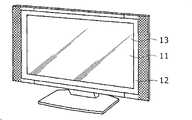
图19示出本发明应用到的电视机。该电视机包括由前面板12、滤色玻璃13等构成的视频显示屏幕11。使用根据本发明的实施方式的显示装置作为视频显示屏幕11来制造该电视机。Fig. 19 shows a television set to which the present invention is applied. The television includes a
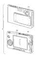
图20示出本发明应用到的数字照相机。图20的上面部分为正面图,而图20的下面部分为后视图。该数字照相机包括图像拾取镜、闪光用发光单元15、显示单元16、控制开关、菜单开关和快门19。使用根据本发明的实施方式的显示装置作为显示单元16来制造该数字照相机。Fig. 20 shows a digital camera to which the present invention is applied. The upper part of FIG. 20 is a front view, and the lower part of FIG. 20 is a rear view. The digital camera includes an image pickup mirror, a
图21示出本发明应用到的膝上型个人计算机。该膝上型个人计算机的主体单元20包括操作来输入字符的键盘21等,而该膝上型个人计算机的主体单元盖包括显示图像的显示单元22。使用根据本发明的实施方式的显示装置作为显示单元22来制造该膝上型个人计算机。Fig. 21 shows a laptop personal computer to which the present invention is applied. A
图22示出本发明应用到的便携式终端装置,图22的左边部分示出了打开状态,而图22的右边部分示出了合上状态。便携式终端装置包括上侧外壳23、下侧外壳24、耦合部分(在这种情况下为铰链部分)25、显示器26、副显示器27、画面灯28和照相机29。使用根据本发明的实施方式的显示装置作为显示器26和副显示器27来制造该便携式终端装置。FIG. 22 shows a portable terminal device to which the present invention is applied, the left part of FIG. 22 shows an open state, and the right part of FIG. 22 shows a closed state. The portable terminal device includes an
图23示出本发明应用到的摄影机。该摄影机包括主体单元30、置于面向前面侧上用于拍摄景物画面的镜头34、画面拍摄的时间的开始/停止开关35以及监视器36。使用根据本发明的实施方式的显示装置作为监视器36来制造该摄影机。Fig. 23 shows a video camera to which the present invention is applied. The video camera includes a
本领域技术人员应该理解,依赖于设计要求和其他因素,只要它们在附属权利要求或其等效物的范围内,可以出现各种修改、组合、部分组合和变更。It should be understood by those skilled in the art that various modifications, combinations, sub-combinations and alterations may occur depending on design requirements and other factors as long as they are within the scope of the appended claims or the equivalents thereof.
Claims (5)
Translated fromChineseApplications Claiming Priority (2)
| Application Number | Priority Date | Filing Date | Title |
|---|---|---|---|
| JP133864/07 | 2007-05-21 | ||
| JP2007133864AJP2008287141A (en) | 2007-05-21 | 2007-05-21 | Display device, its driving method, and electronic equipment |
Publications (2)
| Publication Number | Publication Date |
|---|---|
| CN101312012Atrue CN101312012A (en) | 2008-11-26 |
| CN101312012B CN101312012B (en) | 2011-03-23 |
Family
ID=40071959
Family Applications (1)
| Application Number | Title | Priority Date | Filing Date |
|---|---|---|---|
| CN200810107933.5AActiveCN101312012B (en) | 2007-05-21 | 2008-05-21 | Display device, driving method thereof, and electronic device |
Country Status (5)
| Country | Link |
|---|---|
| US (1) | US8988320B2 (en) |
| JP (1) | JP2008287141A (en) |
| KR (1) | KR20080103000A (en) |
| CN (1) | CN101312012B (en) |
| TW (1) | TWI407407B (en) |
Cited By (10)
| Publication number | Priority date | Publication date | Assignee | Title |
|---|---|---|---|---|
| CN101770737A (en)* | 2009-01-06 | 2010-07-07 | 统宝光电股份有限公司 | Image display system and display panel |
| CN101667418B (en)* | 2009-09-25 | 2012-03-28 | 深圳丹邦投资集团有限公司 | Method for displaying luminance compensation of display screen and system thereof |
| CN102549646A (en)* | 2010-09-06 | 2012-07-04 | 松下电器产业株式会社 | Display device and method of driving same |
| CN101770745B (en)* | 2008-12-17 | 2012-09-05 | 索尼株式会社 | Display device, display device drive method, and electronic apparatus |
| CN104282260A (en)* | 2013-07-08 | 2015-01-14 | 索尼公司 | Display device, driving method for display device, and electronic device |
| CN108701435A (en)* | 2016-06-20 | 2018-10-23 | 索尼公司 | Display devices and electronics |
| CN108766352A (en)* | 2012-11-14 | 2018-11-06 | 索尼公司 | Light-emitting component, display device and electronic device |
| CN104282257B (en)* | 2013-07-08 | 2019-04-05 | 索尼公司 | Display device, driving method for display device, and electronic device |
| CN111105751A (en)* | 2012-12-26 | 2020-05-05 | 索尼公司 | Display device, method for driving the same, and electronic apparatus |
| CN111681611A (en)* | 2020-06-11 | 2020-09-18 | 昆山国显光电有限公司 | Pixel circuit and display device |
Families Citing this family (13)
| Publication number | Priority date | Publication date | Assignee | Title |
|---|---|---|---|---|
| JP2010002498A (en)* | 2008-06-18 | 2010-01-07 | Sony Corp | Panel and drive control method |
| JP5157825B2 (en) | 2008-10-29 | 2013-03-06 | ソニー株式会社 | Manufacturing method of organic EL display |
| JP5308796B2 (en)* | 2008-11-28 | 2013-10-09 | グローバル・オーエルイーディー・テクノロジー・リミテッド・ライアビリティ・カンパニー | Display device and pixel circuit |
| JP5287210B2 (en)* | 2008-12-17 | 2013-09-11 | ソニー株式会社 | Display device and electronic device |
| JP5299126B2 (en)* | 2009-07-01 | 2013-09-25 | セイコーエプソン株式会社 | LIGHT-EMITTING DEVICE, ELECTRONIC DEVICE, AND METHOD FOR DRIVING PIXEL CIRCUIT |
| KR101692367B1 (en)* | 2010-07-22 | 2017-01-04 | 삼성디스플레이 주식회사 | Pixel and Organic Light Emitting Display Device Using the Same |
| JP6164059B2 (en) | 2013-11-15 | 2017-07-19 | ソニー株式会社 | Display device, electronic apparatus, and display device driving method |
| JP2015187672A (en)* | 2014-03-27 | 2015-10-29 | ソニー株式会社 | Display device, driving method of display device and electronic apparatus |
| JP2016062076A (en) | 2014-09-22 | 2016-04-25 | Nltテクノロジー株式会社 | Pixel circuit, method for driving the same and display device |
| JP2017026973A (en) | 2015-07-28 | 2017-02-02 | ソニー株式会社 | Display panel, display device and electronic apparatus |
| CN105206217B (en)* | 2015-10-27 | 2018-02-06 | 京东方科技集团股份有限公司 | display processing method, device and display device |
| KR102595130B1 (en) | 2017-12-07 | 2023-10-26 | 엘지디스플레이 주식회사 | Light emitting display apparatus and method for driving thereof |
| CN115862531B (en)* | 2023-03-03 | 2023-04-18 | 北京数字光芯集成电路设计有限公司 | A voltage-input pixel drive circuit applied to a microdisplay panel |
Family Cites Families (21)
| Publication number | Priority date | Publication date | Assignee | Title |
|---|---|---|---|---|
| JP3956347B2 (en) | 2002-02-26 | 2007-08-08 | インターナショナル・ビジネス・マシーンズ・コーポレーション | Display device |
| JP3613253B2 (en) | 2002-03-14 | 2005-01-26 | 日本電気株式会社 | Current control element drive circuit and image display device |
| JP4195337B2 (en) | 2002-06-11 | 2008-12-10 | 三星エスディアイ株式会社 | Light emitting display device, display panel and driving method thereof |
| JP2004093682A (en) | 2002-08-29 | 2004-03-25 | Toshiba Matsushita Display Technology Co Ltd | Electroluminescence display panel, driving method of electroluminescence display panel, driving circuit of electroluminescence display apparatus and electroluminescence display apparatus |
| GB0220614D0 (en)* | 2002-09-05 | 2002-10-16 | Koninkl Philips Electronics Nv | Electroluminescent display devices |
| GB0223305D0 (en) | 2002-10-08 | 2002-11-13 | Koninkl Philips Electronics Nv | Electroluminescent display devices |
| JP3832415B2 (en) | 2002-10-11 | 2006-10-11 | ソニー株式会社 | Active matrix display device |
| KR100497246B1 (en)* | 2003-04-01 | 2005-06-23 | 삼성에스디아이 주식회사 | Light emitting display device and display panel and driving method thereof |
| US6998788B2 (en)* | 2003-06-11 | 2006-02-14 | Au Optronics Corporation | Architecture of data driver applied at display elements with current-driven pixels |
| JP2005099715A (en)* | 2003-08-29 | 2005-04-14 | Seiko Epson Corp | Electronic circuit driving method, electronic circuit, electronic device, electro-optical device, electronic apparatus, and electronic device driving method |
| TWI286654B (en)* | 2003-11-13 | 2007-09-11 | Hannstar Display Corp | Pixel structure in a matrix display and driving method thereof |
| JP2005151015A (en)* | 2003-11-13 | 2005-06-09 | Sony Corp | Display and its driving method |
| GB0400213D0 (en)* | 2004-01-07 | 2004-02-11 | Koninkl Philips Electronics Nv | Electroluminescent display devices |
| US20050275352A1 (en)* | 2004-06-14 | 2005-12-15 | Au Optronics Corporation. | Redundant storage capacitor and method for repairing OLED pixels and driving circuits |
| KR101080351B1 (en)* | 2004-06-22 | 2011-11-04 | 삼성전자주식회사 | Display device and driving method thereof |
| KR100604058B1 (en)* | 2004-09-24 | 2006-07-24 | 삼성에스디아이 주식회사 | DC / DC converter, light emitting display using same and driving method thereof |
| GB0425188D0 (en)* | 2004-11-16 | 2004-12-15 | Koninkl Philips Electronics Nv | Active matrix display devices |
| US20060164345A1 (en) | 2005-01-26 | 2006-07-27 | Honeywell International Inc. | Active matrix organic light emitting diode display |
| JP4923410B2 (en)* | 2005-02-02 | 2012-04-25 | ソニー株式会社 | Pixel circuit and display device |
| TWI282537B (en)* | 2005-04-21 | 2007-06-11 | Au Optronics Corp | Display units |
| US8344970B2 (en)* | 2005-10-12 | 2013-01-01 | Koninklijke Philips Electronics N.V. | Transistor control circuits and control methods, and active matrix display devices using the same |
- 2007
- 2007-05-21JPJP2007133864Apatent/JP2008287141A/enactivePending
- 2008
- 2008-05-01USUS12/149,452patent/US8988320B2/enactiveActive
- 2008-05-14TWTW097117736Apatent/TWI407407B/ennot_activeIP Right Cessation
- 2008-05-21CNCN200810107933.5Apatent/CN101312012B/enactiveActive
- 2008-05-21KRKR1020080046960Apatent/KR20080103000A/ennot_activeCeased
Cited By (21)
| Publication number | Priority date | Publication date | Assignee | Title |
|---|---|---|---|---|
| CN101770745B (en)* | 2008-12-17 | 2012-09-05 | 索尼株式会社 | Display device, display device drive method, and electronic apparatus |
| CN101770737A (en)* | 2009-01-06 | 2010-07-07 | 统宝光电股份有限公司 | Image display system and display panel |
| CN101770737B (en)* | 2009-01-06 | 2013-09-11 | 群创光电股份有限公司 | Image display system and display panel |
| CN101667418B (en)* | 2009-09-25 | 2012-03-28 | 深圳丹邦投资集团有限公司 | Method for displaying luminance compensation of display screen and system thereof |
| CN102549646A (en)* | 2010-09-06 | 2012-07-04 | 松下电器产业株式会社 | Display device and method of driving same |
| CN102549646B (en)* | 2010-09-06 | 2014-07-16 | 松下电器产业株式会社 | Display device and method of driving same |
| CN109147671A (en)* | 2012-11-14 | 2019-01-04 | 索尼公司 | Light-emitting component |
| CN108766352A (en)* | 2012-11-14 | 2018-11-06 | 索尼公司 | Light-emitting component, display device and electronic device |
| CN111105751A (en)* | 2012-12-26 | 2020-05-05 | 索尼公司 | Display device, method for driving the same, and electronic apparatus |
| CN111105751B (en)* | 2012-12-26 | 2023-09-26 | 索尼公司 | Display device, method for driving the same, and electronic apparatus |
| CN110097848A (en)* | 2013-07-08 | 2019-08-06 | 索尼公司 | Display device, driving method and electronic equipment for display device |
| CN104282257B (en)* | 2013-07-08 | 2019-04-05 | 索尼公司 | Display device, driving method for display device, and electronic device |
| CN109920376A (en)* | 2013-07-08 | 2019-06-21 | 索尼公司 | Display device, driving method and electronic equipment for display device |
| CN104282260B (en)* | 2013-07-08 | 2018-05-29 | 索尼公司 | Display device, driving method for display device, and electronic device |
| CN104282260A (en)* | 2013-07-08 | 2015-01-14 | 索尼公司 | Display device, driving method for display device, and electronic device |
| US11462159B2 (en) | 2013-07-08 | 2022-10-04 | Sony Group Corporation | Display device, driving method for display device and electronic apparatus |
| US11282460B2 (en) | 2016-06-20 | 2022-03-22 | Sony Group Corporation | Display apparatus and electronic apparatus |
| US11705070B2 (en) | 2016-06-20 | 2023-07-18 | Sony Group Corporation | Display apparatus and electronic apparatus |
| CN108701435A (en)* | 2016-06-20 | 2018-10-23 | 索尼公司 | Display devices and electronics |
| CN111681611A (en)* | 2020-06-11 | 2020-09-18 | 昆山国显光电有限公司 | Pixel circuit and display device |
| CN111681611B (en)* | 2020-06-11 | 2021-06-25 | 昆山国显光电有限公司 | Pixel circuit and display device |
Also Published As
| Publication number | Publication date |
|---|---|
| JP2008287141A (en) | 2008-11-27 |
| CN101312012B (en) | 2011-03-23 |
| US20080291182A1 (en) | 2008-11-27 |
| TW200907900A (en) | 2009-02-16 |
| TWI407407B (en) | 2013-09-01 |
| US8988320B2 (en) | 2015-03-24 |
| KR20080103000A (en) | 2008-11-26 |
Similar Documents
| Publication | Publication Date | Title |
|---|---|---|
| CN101312012B (en) | Display device, driving method thereof, and electronic device | |
| CN101312008B (en) | Display device, display device driving method, and electronic device | |
| JP4297169B2 (en) | Display device, driving method thereof, and electronic apparatus | |
| CN101312007B (en) | Display device, driving method thereof, and electronic device | |
| US20140320472A1 (en) | Display apparatus and driving method therefor | |
| TWI402802B (en) | Display device, method for driving the same, and electronic apparatus | |
| KR101498571B1 (en) | Display, method for driving display, electronic apparatus | |
| JP2009168969A (en) | Display device, driving method thereof, and electronic apparatus | |
| US8384627B2 (en) | Display device and electronic equipment | |
| US8022905B2 (en) | Display device, driving method of the same and electronic apparatus using the same | |
| US8022904B2 (en) | Display device, driving method of the same and electronic apparatus using the same | |
| KR20080087708A (en) | Display device, driving method thereof, and electronic device | |
| CN101504824B (en) | Display apparatus, driving method therefore and electronic apparatus | |
| JP2009080367A (en) | Display device, its driving method, and electronic equipment | |
| JP4985303B2 (en) | Display device, driving method thereof, and electronic apparatus | |
| US8199143B2 (en) | Display apparatus, driving method for display apparatus and electronic apparatus | |
| JP2009098430A (en) | Display device and electronic apparatus | |
| JP2010122604A (en) | Display device and electronic equipment | |
| JP2009098431A (en) | Display device and electronic apparatus |
Legal Events
| Date | Code | Title | Description |
|---|---|---|---|
| C06 | Publication | ||
| PB01 | Publication | ||
| C10 | Entry into substantive examination | ||
| SE01 | Entry into force of request for substantive examination | ||
| C14 | Grant of patent or utility model | ||
| GR01 | Patent grant | ||
| ASS | Succession or assignment of patent right | Owner name:JANPAN ORGANIC RATE DISPLAY CO., LTD. Free format text:FORMER OWNER: SONY CORPORATION Effective date:20150730 | |
| C41 | Transfer of patent application or patent right or utility model | ||
| TR01 | Transfer of patent right | Effective date of registration:20150730 Address after:Tokyo, Japan Patentee after:JOLED Inc. Address before:Tokyo, Japan Patentee before:Sony Corp. | |
| TR01 | Transfer of patent right | ||
| TR01 | Transfer of patent right | Effective date of registration:20231122 Address after:Tokyo, Japan Patentee after:Japan Display Design and Development Contract Society Address before:Tokyo, Japan Patentee before:JOLED Inc. | |
| TR01 | Transfer of patent right | Effective date of registration:20250729 Address after:Tokyo, Japan Patentee after:Magno Bolan Co.,Ltd. Country or region after:Japan Address before:Tokyo, Japan Patentee before:Japan Display Design and Development Contract Society Country or region before:Japan | |
| TR01 | Transfer of patent right |