CN101310369A - Method for manufacturing semiconductor device and semiconductor device obtained by the method - Google Patents
Method for manufacturing semiconductor device and semiconductor device obtained by the methodDownload PDFInfo
- Publication number
- CN101310369A CN101310369ACNA2006800426277ACN200680042627ACN101310369ACN 101310369 ACN101310369 ACN 101310369ACN A2006800426277 ACNA2006800426277 ACN A2006800426277ACN 200680042627 ACN200680042627 ACN 200680042627ACN 101310369 ACN101310369 ACN 101310369A
- Authority
- CN
- China
- Prior art keywords
- mesa
- semiconductor region
- shaped semiconductor
- insulating barrier
- insulating layer
- Prior art date
- Legal status (The legal status is an assumption and is not a legal conclusion. Google has not performed a legal analysis and makes no representation as to the accuracy of the status listed.)
- Pending
Links
Images


Classifications
- B—PERFORMING OPERATIONS; TRANSPORTING
- B82—NANOTECHNOLOGY
- B82Y—SPECIFIC USES OR APPLICATIONS OF NANOSTRUCTURES; MEASUREMENT OR ANALYSIS OF NANOSTRUCTURES; MANUFACTURE OR TREATMENT OF NANOSTRUCTURES
- B82Y10/00—Nanotechnology for information processing, storage or transmission, e.g. quantum computing or single electron logic
- H—ELECTRICITY
- H01—ELECTRIC ELEMENTS
- H01L—SEMICONDUCTOR DEVICES NOT COVERED BY CLASS H10
- H01L21/00—Processes or apparatus adapted for the manufacture or treatment of semiconductor or solid state devices or of parts thereof
- H01L21/02—Manufacture or treatment of semiconductor devices or of parts thereof
- H01L21/02104—Forming layers
- H01L21/02107—Forming insulating materials on a substrate
- H01L21/02109—Forming insulating materials on a substrate characterised by the type of layer, e.g. type of material, porous/non-porous, pre-cursors, mixtures or laminates
- H01L21/02112—Forming insulating materials on a substrate characterised by the type of layer, e.g. type of material, porous/non-porous, pre-cursors, mixtures or laminates characterised by the material of the layer
- H01L21/02123—Forming insulating materials on a substrate characterised by the type of layer, e.g. type of material, porous/non-porous, pre-cursors, mixtures or laminates characterised by the material of the layer the material containing silicon
- H01L21/02164—Forming insulating materials on a substrate characterised by the type of layer, e.g. type of material, porous/non-porous, pre-cursors, mixtures or laminates characterised by the material of the layer the material containing silicon the material being a silicon oxide, e.g. SiO2
- H—ELECTRICITY
- H01—ELECTRIC ELEMENTS
- H01L—SEMICONDUCTOR DEVICES NOT COVERED BY CLASS H10
- H01L21/00—Processes or apparatus adapted for the manufacture or treatment of semiconductor or solid state devices or of parts thereof
- H01L21/02—Manufacture or treatment of semiconductor devices or of parts thereof
- H01L21/02104—Forming layers
- H01L21/02107—Forming insulating materials on a substrate
- H01L21/02225—Forming insulating materials on a substrate characterised by the process for the formation of the insulating layer
- H01L21/0226—Forming insulating materials on a substrate characterised by the process for the formation of the insulating layer formation by a deposition process
- H01L21/02263—Forming insulating materials on a substrate characterised by the process for the formation of the insulating layer formation by a deposition process deposition from the gas or vapour phase
- H01L21/02271—Forming insulating materials on a substrate characterised by the process for the formation of the insulating layer formation by a deposition process deposition from the gas or vapour phase deposition by decomposition or reaction of gaseous or vapour phase compounds, i.e. chemical vapour deposition
- H01L21/02274—Forming insulating materials on a substrate characterised by the process for the formation of the insulating layer formation by a deposition process deposition from the gas or vapour phase deposition by decomposition or reaction of gaseous or vapour phase compounds, i.e. chemical vapour deposition in the presence of a plasma [PECVD]
- H—ELECTRICITY
- H01—ELECTRIC ELEMENTS
- H01L—SEMICONDUCTOR DEVICES NOT COVERED BY CLASS H10
- H01L21/00—Processes or apparatus adapted for the manufacture or treatment of semiconductor or solid state devices or of parts thereof
- H01L21/02—Manufacture or treatment of semiconductor devices or of parts thereof
- H01L21/02104—Forming layers
- H01L21/02107—Forming insulating materials on a substrate
- H01L21/02296—Forming insulating materials on a substrate characterised by the treatment performed before or after the formation of the layer
- H01L21/02299—Forming insulating materials on a substrate characterised by the treatment performed before or after the formation of the layer pre-treatment
- H01L21/02304—Forming insulating materials on a substrate characterised by the treatment performed before or after the formation of the layer pre-treatment formation of intermediate layers, e.g. buffer layers, layers to improve adhesion, lattice match or diffusion barriers
- H—ELECTRICITY
- H01—ELECTRIC ELEMENTS
- H01L—SEMICONDUCTOR DEVICES NOT COVERED BY CLASS H10
- H01L21/00—Processes or apparatus adapted for the manufacture or treatment of semiconductor or solid state devices or of parts thereof
- H01L21/70—Manufacture or treatment of devices consisting of a plurality of solid state components formed in or on a common substrate or of parts thereof; Manufacture of integrated circuit devices or of parts thereof
- H01L21/71—Manufacture of specific parts of devices defined in group H01L21/70
- H01L21/76—Making of isolation regions between components
- H01L21/762—Dielectric regions, e.g. EPIC dielectric isolation, LOCOS; Trench refilling techniques, SOI technology, use of channel stoppers
- H01L21/76224—Dielectric regions, e.g. EPIC dielectric isolation, LOCOS; Trench refilling techniques, SOI technology, use of channel stoppers using trench refilling with dielectric materials
- H01L21/76232—Dielectric regions, e.g. EPIC dielectric isolation, LOCOS; Trench refilling techniques, SOI technology, use of channel stoppers using trench refilling with dielectric materials of trenches having a shape other than rectangular or V-shape, e.g. rounded corners, oblique or rounded trench walls
Landscapes
- Engineering & Computer Science (AREA)
- Physics & Mathematics (AREA)
- Condensed Matter Physics & Semiconductors (AREA)
- General Physics & Mathematics (AREA)
- Manufacturing & Machinery (AREA)
- Computer Hardware Design (AREA)
- Microelectronics & Electronic Packaging (AREA)
- Power Engineering (AREA)
- Chemical & Material Sciences (AREA)
- Nanotechnology (AREA)
- Plasma & Fusion (AREA)
- Chemical Kinetics & Catalysis (AREA)
- Mathematical Physics (AREA)
- Theoretical Computer Science (AREA)
- Crystallography & Structural Chemistry (AREA)
- Bipolar Transistors (AREA)
- Electrodes Of Semiconductors (AREA)
- Internal Circuitry In Semiconductor Integrated Circuit Devices (AREA)
Abstract
Translated fromChineseDescription
Translated fromChinese技术领域technical field
本发明涉及制造半导体器件的方法,该半导体器件具有衬底和至少具有一个半导体元件的半导体主体,其中在半导体主体的表面上形成了台面状半导体区域,在台面状半导体区域上沉积了绝缘层,其中该绝缘层在台面状半导体区域顶部的厚度小于其在与该台面状半导体区域邻接的区域中的厚度,随后去除绝缘层在台面状半导体区域顶部的部分,从而露出台面状半导体区域的上面,并且随后在所得到的结构上沉积与台面状半导体区域接触的导电层。本发明还涉及采用此方法获得的半导体器件。The invention relates to a method for producing a semiconductor device having a substrate and a semiconductor body having at least one semiconductor element, wherein a mesa-shaped semiconductor region is formed on the surface of the semiconductor body, an insulating layer is deposited on the mesa-shaped semiconductor region, wherein the thickness of the insulating layer at the top of the mesa-shaped semiconductor region is less than its thickness in a region adjoining the mesa-shaped semiconductor region, and subsequently removing a portion of the insulating layer at the top of the mesa-shaped semiconductor region, thereby exposing the top of the mesa-shaped semiconductor region, And subsequently a conductive layer in contact with the mesa-shaped semiconductor regions is deposited on the resulting structure. The invention also relates to semiconductor devices obtained by this method.
这种方法很适合制造类似IC(集成电路)的半导体器件或诸如包括纳米线元件的分立器件之类的其它器件。在这里,具有纳米线的主体至少具有一个介于0.5nm到100nm之间尤其是介于1nm到50nm之间的侧向尺寸。优选地,纳米线在两个侧向方向上具有介于所述范围的尺寸。在这里还应该注意,在半导体工艺中,接触半导体中的极其小的尺寸是具有挑战的技术。然而,虽然台面状半导体区域被设计为尤其包括纳米线,但是本发明也适用于具有其它尺寸的台面状半导体区域。台面状区域意味着该区域在半导体主体的表面上形成了突起。This method is well suited for the fabrication of semiconductor devices like ICs (Integrated Circuits) or other devices such as discrete devices including nanowire elements. Here, the body with the nanowires has at least one lateral dimension between 0.5 nm and 100 nm, in particular between 1 nm and 50 nm. Preferably, the nanowires have dimensions in both lateral directions between said ranges. It should also be noted here that contacting extremely small dimensions in semiconductors is a challenging technique in semiconductor processing. However, although the mesa-shaped semiconductor regions are designed notably to comprise nanowires, the invention is also applicable to mesa-shaped semiconductor regions having other dimensions. A mesa-like region means that the region forms a protrusion on the surface of the semiconductor body.
背景技术Background technique
从在2003年10月9日已经出版的第2003/0189202号US专利申请中已知如在首段中所提到的方法。在该文献中,在硅衬底上提供了包括单晶纳米线的许多台面状半导体区域。在生长了纳米线后,在纳米线上沉积绝缘层以使得所述纳米线上的所述层的厚度小于邻接所述纳米线的区域(例如两个相邻纳米线之间的区域)中的所述层的厚度。采用CVD(化学气相沉积)或旋涂玻璃或喷涂高分子材料层技术来沉积绝缘层。随后,采用例如CMP(化学机械抛光)来使绝缘层平整化。随后,例如用类似金属层的导电层来覆盖纳米线的上表面(该表面是露出来的)。根据所述文献,可以采用这种方法来形成类似传感器或用于显示器的场发射器之类的各类半导体器件。A method as mentioned in the opening paragraph is known from US Patent Application No. 2003/0189202 already published on October 9, 2003. In this document, a number of mesa-shaped semiconductor regions comprising single-crystal nanowires are provided on a silicon substrate. After the nanowires have been grown, an insulating layer is deposited on the nanowires such that the thickness of the layer on the nanowires is less than that in regions adjoining the nanowires (e.g., the region between two adjacent nanowires). The thickness of the layer. The insulating layer is deposited using CVD (Chemical Vapor Deposition) or spin-on-glass or spray-on polymer layer techniques. Subsequently, the insulating layer is planarized using, for example, CMP (Chemical Mechanical Polishing). Subsequently, the upper surface of the nanowires (this surface is exposed) is covered, for example with a conductive layer like a metal layer. According to said document, this method can be used to form various types of semiconductor devices like sensors or field emitters for displays.
这种方法的缺点是它不适于类似晶体管的半导体器件,该晶体管包括例如用于接触晶体管的源极或漏极区域或者发射极或集电极区域的纳米线。尤其是,CVD产生的绝缘层的厚度特别不均匀,而且旋涂或喷涂技术不适合具有极小侧向尺寸的突起的器件,例如纳米线形式的精密突起的情况。这考虑到了所涉及到的类似于温度的工艺条件。A disadvantage of this approach is that it is not suitable for semiconductor devices like transistors comprising, for example, nanowires for contacting the source or drain regions or the emitter or collector regions of the transistor. In particular, the thickness of the CVD-generated insulating layer is particularly non-uniform, and spin-coating or spray-coating techniques are not suitable for devices with protrusions of extremely small lateral dimensions, such as the case of delicate protrusions in the form of nanowires. This takes into account the process conditions like temperature involved.
发明内容Contents of the invention
因此,本发明的目的是避免上述缺点,并且提供一种方法,该方法适于制造包括晶体管的半导体器件,该晶体管包括具有突起(尤其是纳米线)的极小有源区。It is therefore an object of the present invention to avoid the above-mentioned disadvantages and to provide a method suitable for manufacturing a semiconductor device comprising a transistor comprising a very small active area with protrusions, in particular nanowires.
为了实现该目标,首段中所述类型的方法的特征在于采用了高密度等离子体沉积工艺来沉积绝缘层。由于同时沉积和溅射,高密度等离子体沉积具有自平整特性,其中例如在类似纳米线的非常精细的结构的阵列上沉积氧化物。因此,这种纳米线顶部的厚度可以显著小于在具有更大(得多)的侧向尺寸特性上所获得的厚度。而且,用这种方法在台面顶部所获得的材料可以易于被蚀刻,从而露出台面状区域(纳米线)的上面,同时由于用这种方法所沉积的绝缘层的锥形特性而使得台面的侧面保持绝缘。而且,允许采用简单蚀刻步骤来露出台面的表面,这个步骤在不破坏或改变台面结构(顶部)的情况下是可行的。否则,台面顶部在纳米线的情况下是易于被损坏和被改变的。In order to achieve this goal, a method of the type mentioned in the opening paragraph is characterized in that a high-density plasma deposition process is used to deposit the insulating layer. Due to simultaneous deposition and sputtering, high-density plasma deposition has self-levelling properties, where for example oxides are deposited on arrays of very fine structures like nanowires. Thus, the thickness of such nanowire tops can be significantly smaller than that obtained on properties with larger (much) larger lateral dimensions. Moreover, the material obtained in this way on top of the mesas can be easily etched, exposing the tops of the mesa-like regions (nanowires), while the sides of the mesas are exposed due to the tapered nature of the insulating layer deposited in this way. Keep it insulated. Furthermore, a simple etching step is allowed to expose the surface of the mesa, which is possible without destroying or altering the mesa structure (top). Otherwise, the mesa tops are vulnerable to damage and alteration in the case of nanowires.
由于沉积速度和溅射速度的比率在HDP(氧化物)沉积期间是受控微调的,所以可以很好地控制小面积结构顶部上的绝缘层和大面积顶部上的绝缘层之间的厚度比。Since the ratio of deposition rate and sputtering rate is controlled and fine-tuned during HDP (oxide) deposition, the thickness ratio between the insulating layer on top of small-area structures and the insulating layer on top of large-area structures can be well controlled .
在优选的实施例中,采用蚀刻(优选为湿法)步骤来露出台面状半导体区域的上面。这种蚀刻步骤是很容易极具选择性的,而这又非常适合于不破坏或改变台面的上部,尤其是纳米线的上部。而且露出了上表面的纳米线/台面的高度变化可以很小。类似于CMP的工艺易于使这个高度扩展到大晶片上。如果绝缘层包括二氧化硅,则可以使用基于氟化氢的蚀刻剂。在绝缘层为氮化硅的情况下,可以使用基于热磷酸的蚀刻剂。In a preferred embodiment, an etching (preferably wet) step is used to expose the upper side of the mesa-shaped semiconductor region. This etching step is easily very selective, which in turn is well suited to not destroy or alter the upper part of the mesa, especially the upper part of the nanowire. Furthermore, the height variation of the nanowires/mesas exposed on the upper surface can be very small. CMP-like processes readily scale this height to large wafers. If the insulating layer includes silicon dioxide, a hydrogen fluoride-based etchant may be used. Where the insulating layer is silicon nitride, a hot phosphoric acid based etchant may be used.
在另一优选实施例中,在沉积绝缘层之前,沉积了厚度小于该绝缘层的另一绝缘层,另一绝缘层是采用保形沉积工艺来沉积的。在绝缘层的高密度等离子体沉积的开始时,该另一绝缘层可以防止台面状半导体区域在凹蚀期间可能出现的形状或表面的变化。该另一绝缘层的适合厚度可以介于5nm到25nm之间,而绝缘层具有大厚度(例如大约为台面状半导体区域的高度),该绝缘层厚度可在例如50nm到500nm之间变化。适合于这种均匀/保形的另一绝缘层的工艺是CVD,例如在另一绝缘层为二氧化硅的情况下使用TEOS(正硅酸乙酯)。In another preferred embodiment, prior to the deposition of the insulating layer, another insulating layer having a thickness smaller than the insulating layer is deposited, the further insulating layer being deposited using a conformal deposition process. At the beginning of the high-density plasma deposition of the insulating layer, this further insulating layer prevents possible changes in shape or surface of the mesa-shaped semiconductor regions during etchback. A suitable thickness of this further insulating layer may be between 5nm and 25nm, whereas the insulating layer has a large thickness (for example about the height of the mesa-shaped semiconductor region), the thickness of the insulating layer may vary for example between 50nm and 500nm. A suitable process for such a uniform/conformal another insulating layer is CVD, for example using TEOS (tetraethyl silicate) in the case of another insulating layer of silicon dioxide.
如果绝缘层和另一绝缘层包括同样的材料,则可以采用单蚀刻步骤来实现台面上面的露出。二氧化硅是非常适合于该目的的材料。If the insulating layer and the further insulating layer comprise the same material, a single etching step can be used to achieve the exposure above the mesa. Silica is a very suitable material for this purpose.
在另一优选实施例中,在露出台面状半导体区域的上面之后,在该表面上形成了与台面状半导体区域接触的接触区域,该接触区域包括金属硅化物并且其侧向尺寸大于台面状半导体区域。该接触区域尤其适于接触场效应晶体管的源极/漏极区域或双极型晶体管的发射极/集电极区域。In another preferred embodiment, after exposing the upper surface of the mesa-shaped semiconductor region, a contact region to contact the mesa-shaped semiconductor region is formed on the surface, the contact region includes metal silicide and its lateral dimension is larger than that of the mesa-shaped semiconductor region. area. The contact region is especially suitable for contacting a source/drain region of a field effect transistor or an emitter/collector region of a bipolar transistor.
优选地,接触区域是这样形成的:沉积多晶硅层和金属层,在形成金属硅化物前至少使多晶硅层形成图形。用这种方法,硅化物形成是自对准的。可以在已形成图形的多晶硅层形成之前或之后,或者既在此之前又在此之后,沉积金属层。在后一情况中,两个金属层实际上被用于形成硅化物。Preferably, the contact area is formed by depositing a polysilicon layer and a metal layer, at least patterning the polysilicon layer before forming the metal suicide. In this way, the silicide formation is self-aligned. The metal layer may be deposited either before or after, or both, the formation of the patterned polysilicon layer. In the latter case, two metal layers are actually used to form the silicide.
然而,优选地,在沉积已形成图形的多晶硅层后,沉积金属层。用这种方法,接触区域中的金属硅化物成分的后期均匀性可以很高。而且,在高掺杂多晶硅层的情况下,可将额外的掺杂原子从该层驱赶进纳米线的上部分,例如,纳米线形成了双极型晶体管的发射极或集电极。通过采用选择性(湿法)蚀刻可很容易地实现将接触区域顶部上的金属层的残留部分去除,或在万一存在的情况下将所述区域外部的金属层的残留部分去除。优选地,通过RTA(快速热退火)步骤来完成掺杂原子从多晶硅层外扩散进入纳米线的纳米线掺杂。而且,在此优选实施例中,由于所谓的雪犁效应(snow-plow effects)会将掺杂原子推向与移动的金属硅化物硅界面邻接的硅区,所以在硅化步骤期间可以获得纳米线的额外更强的掺杂。Preferably, however, the metal layer is deposited after the patterned polysilicon layer is deposited. In this way, the post-homogeneity of the metal suicide composition in the contact area can be very high. Also, in the case of a highly doped polysilicon layer, additional dopant atoms can be driven from this layer into the upper part of the nanowires, eg the nanowires forming the emitter or collector of a bipolar transistor. Removal of the remaining portion of the metal layer on top of the contact area, or outside the area if present, can be easily achieved by employing a selective (wet) etch. The doping of the nanowires with out-diffusion of dopant atoms from the polysilicon layer into the nanowires is preferably done by an RTA (Rapid Thermal Annealing) step. Furthermore, in this preferred embodiment, nanowires are obtained during the silicidation step due to the so-called snow-plow effects that push dopant atoms towards the silicon regions adjacent to the mobile metal silicide-silicon interface. additional stronger doping.
优选地,将绝缘层和另一绝缘层的厚度选择为大约等于台面状半导体区域的高度。由于绝缘区域的锥形特性,在台面的上表面通过蚀刻已露出后,绝缘材料仍可覆盖台面的侧面。Preferably, the thicknesses of the insulating layer and of the further insulating layer are chosen approximately equal to the height of the mesa-shaped semiconductor region. Due to the tapered nature of the insulating region, the insulating material may still cover the sides of the mesa after the upper surface of the mesa has been exposed by etching.
对于半导体元件,优选地选择晶体管。台面状半导体区域(尤其是纳米线形式)可以形成场效应晶体管的源极/漏极区域的接触部分或可以形成双极型晶体管的发射极或集电极区域(的一部分)。For semiconductor elements, transistors are preferably chosen. A mesa-like semiconductor region, especially in the form of a nanowire, may form a contact part of a source/drain region of a field effect transistor or may form (part of) an emitter or collector region of a bipolar transistor.
最后,本发明还包括通过根据本发明的方法获得的半导体器件。Finally, the invention also includes semiconductor devices obtained by the method according to the invention.
附图说明Description of drawings
参考以下所述的实施例,连同附图,本发明的这些方面和其它方面将是显然的且清楚的,其中:These and other aspects of the invention will be apparent and apparent with reference to the embodiments described hereinafter, taken in conjunction with the accompanying drawings, in which:
图1至图10是在用根据本发明的方法制造半导体器件时各个阶段的半导体器件的截面图,以及1 to 10 are cross-sectional views of a semiconductor device at various stages when a semiconductor device is manufactured by a method according to the present invention, and
图11示出了作为柱直径D的函数的在柱上的高密度等离子体沉积的二氧化硅的厚度d。Figure 11 shows the thickness d of high density plasma deposited silicon dioxide on a pillar as a function of the diameter D of the pillar.
附图是示意性的,并不是按照比例绘制的,为了更清楚的描述,特别扩大了厚度方向的尺寸。在不同附图中,通常给对应部分相同标号和相同的阴影。The drawings are schematic and not drawn to scale, and the dimensions in the thickness direction are particularly exaggerated for a clearer description. Corresponding parts are generally given the same reference numerals and the same hatching in different figures.
具体实施方式Detailed ways
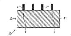
图1至图10是在用根据本发明的方法制造半导体器件时各个相关阶段的半导体器件的截面图。要被制造的半导体器件可包含已经预先处于图1的阶段的半导体元件,可用通常方式形成该半导体元件。例如,该元件可以是场效应晶体管或双极型晶体管。例如,该示例的方法中形成的台面状区域可以是接触结构,其用于场效应晶体管的源极/漏极区域,或双极型晶体管的发射极或反向双极型晶体管的集电极区域。为了简单起见,在图中未示出这种晶体管的特性。1 to 10 are cross-sectional views of a semiconductor device at various relevant stages when the semiconductor device is manufactured by a method according to the present invention. The semiconductor device to be manufactured may comprise semiconductor elements which have previously been at the stage of FIG. 1 , which may be formed in the usual manner. For example, the element may be a field effect transistor or a bipolar transistor. For example, the mesa-like region formed in the method of this example may be a contact structure for the source/drain region of a field effect transistor, or the emitter of a bipolar transistor or the collector region of an inverted bipolar transistor . For simplicity, the characteristics of such transistors are not shown in the figure.
在器件10的制造的第一相关步骤中(见图1),将台面状半导体区域1提供给形成了硅半导体主体12的硅衬底11,在半导体主体中已经(大量地)形成了例如场效应或双极型晶体管,在此纳米线1包括硅。例如,可通过对不均匀沉积层进行光刻和蚀刻,而且通过例如在R.S.Wagner和W.C.Ellis发表在Applied Physics Letters,vol.4,no.5,1,march 1964,pp89-90的“Vapor-liquid-solidmechanism of single crystal growth”中所述的选择性沉积技术来形成这些线1。在该示例中,柱1的高度大约为500nm,其直径大约为50nm。In a first relevant step of the manufacture of the device 10 (see FIG. 1 ), a mesa-shaped
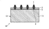
随后(见图2),采用CVD(化学气相沉积)和TEOS(正硅酸乙酯)作为源材料来沉积二氧化硅薄层5。在该示例中,层5的厚度为10nm并且该厚度在每个位置上都基本相同。层2的作用是为细柱1形成锚和保护屏,以防止在随后的同样的二氧化硅绝缘层2的沉积工艺中溅射。然而,现在采用高密度等离子体沉积来完成该沉积。在该工艺中,同时发生沉积和溅射,其中沉积占优势。由于柱1顶部的绝缘层2的厚度比邻接区域3中的绝缘层2的厚度薄,所以这种特殊的沉积工艺具有如在图2中可以看出的自平整化特性。在该示例中,柱1顶部的厚度大约为100nm,其比邻接区域3中的厚度(为500nm)小400nm。对于沉积工艺的使用,同样典型的是在柱1侧面的绝缘层2中可获得锥形15,其对应于45°侧壁角。Subsequently (see FIG. 2 ), a
接下来(见图3),通过选择性针对硅的蚀刻剂来去除柱1顶部的绝缘层2和另一绝缘层5,并且在该示例中该蚀刻剂包括基于氟化氢的蚀刻剂(可能为缓冲剂)。在采用已知蚀刻速度的时基上完成该蚀刻。Next (see FIG. 3 ), the insulating
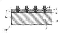
随后(见图4),在该结构上沉积厚度为60nm的多晶硅层6。这可采用例如作为沉积技术的CVD来完成。Subsequently (see FIG. 4 ), a
接下来(见图5),采用光刻和(干法)蚀刻来形成多晶硅层6的图形。这些步骤未被分开示出。形成图形后的聚合孤岛6的直径在该示例中约为500nm并且通常其大小约为有源区的大小。Next (see FIG. 5 ), the
现在(见图6),例如采用溅射或气相沉积技术,在该结构上沉积金属层,在这里是厚度为30nm的镍层。然后在炉子中对该结构进行热处理,热处理的温度范围为280至400℃,在该示例中为300℃。通过该处理,多晶硅区域6与金属层7相互作用以形成金属硅化物,在该示例中为单硅化镍。Now (see FIG. 6 ), a metal layer, here a nickel layer with a thickness of 30 nm, is deposited on the structure, for example using sputtering or vapor deposition techniques. The structure is then heat-treated in a furnace at temperatures ranging from 280 to 400°C, in this example 300°C. Through this process, the
得到的结构(见图7)示出了已经在柱1顶部以自对准方式形成的硅化镍接触区域4。通过选择性蚀刻去除接触区域4外部的镍层7的残留部分。The resulting structure (see FIG. 7 ) shows a
接下来(见图8),采用CVD来沉积PMD(前金属介质)层8,该层8包括厚度约为1000nm的二氧化硅。Next (see FIG. 8 ), CVD is used to deposit a PMD (Pre-Metal Dielectric)
在该步骤之后(见图9),采用光刻和蚀刻在PMD层8中形成接触孔20。After this step (see FIG. 9 ), contact holes 20 are formed in the
最后(见图10),沉积金属层10(例如铝)并且将其制成图形,以便接触更大尺寸的硅化物面积4。在利用类似蚀刻或锯切的分割技术后,获得适于安装的独立器件10。Finally (see FIG. 10 ), a metal layer 10 (eg aluminum) is deposited and patterned in order to contact the
接下来,再次描述高密度等离子体的选择和在其上进行沉积的表面的几何形状的影响。Next, the influence of the choice of high-density plasma and the geometry of the surface on which the deposition takes place is again described.
图11示出了作为柱直径D的函数的在柱上高密度等离子体沉积的二氧化硅的厚度d。针对沉积在平坦的硅衬底上的厚度为500nm的二氧化硅层,获得了该图的结果。曲线110(其示出了在包括直径为D的硅柱的结构硅表面上的沉积厚度d)显示了对于约为500nm的柱直径,沉积厚度基本上与在平坦的晶圆上沉积的情况相同。对于较小的直径D,柱顶部的沉积厚度逐渐减小。例如,对于直径D约为50nm的柱,所述厚度d约为100nm,这比在平坦的晶片上的沉积厚度和两个柱之间的沉积厚度小400nm(假设两个相邻柱之间的距离足够大,例如大于约500nm)。Figure 11 shows the thickness d of high density plasma deposited silicon dioxide on a pillar as a function of the diameter D of the pillar. The results of this figure were obtained for a silicon dioxide layer with a thickness of 500 nm deposited on a flat silicon substrate. Curve 110 (which shows the deposition thickness d on a structured silicon surface comprising silicon pillars of diameter D) shows that for a pillar diameter of about 500 nm, the deposition thickness is essentially the same as for deposition on a flat wafer . For smaller diameters D, the deposition thickness at the top of the pillars gradually decreases. For example, for a pillar with a diameter D of about 50 nm, the thickness d is about 100 nm, which is 400 nm smaller than the deposition thickness on a flat wafer and between two pillars (assuming a distance between two adjacent pillars The distance is sufficiently large, for example greater than about 500 nm).
很明显,本发明不限于在此所述的示例,并且对于所属领域的技术人员而言,在本发明的范围内可进行很多修改和变化。It is obvious that the present invention is not limited to the examples described here, and that many modifications and variations will occur within the scope of the invention to those skilled in the art.
例如,注意,本发明不仅适于制造类似晶体管的分立器件,而且适于制造类似(C)MOS或BI(C)MOS IC以及双极型IC的IC。每个纳米线区域都可以是单个(一部分)器件的一部分,但是使用多个纳米线来形成器件的单个区域或者单个器件的一部分也是可行的。Note, for example, that the invention is not only suitable for making discrete devices like transistors, but also for making ICs like (C)MOS or BI(C)MOS ICs as well as bipolar ICs. Each nanowire region may be part of a single (part of) device, but it is also possible to use multiple nanowires to form a single region of a device or part of a single device.
而且,注意,对单独步骤进行各种改变是可行的。例如可以选择其它的沉积技术来代替在该示例中所用的沉积技术。这同样适用于所选择的材料。因此,(另一)绝缘层可以由例如氮化硅构成。Also, note that various changes to the individual steps are possible. For example, other deposition techniques can be selected instead of the deposition technique used in this example. The same applies to the chosen material. Thus, the (further) insulating layer may consist of, for example, silicon nitride.
最后,再次强调,本发明允许制造具有台面状区域的器件,该台面状区域具有极小的侧向尺寸,例如在纳米线的情况中,纳米线一方面包含大掺杂水平,而另一方面可具有大的接触焊盘。Finally, again, the invention allows the fabrication of devices with mesa-like regions with extremely small lateral dimensions, such as in the case of nanowires, which on the one hand contain large doping levels and on the other hand Can have large contact pads.
Claims (14)
Applications Claiming Priority (2)
| Application Number | Priority Date | Filing Date | Title |
|---|---|---|---|
| EP05110790.2 | 2005-11-16 | ||
| EP05110790 | 2005-11-16 |
Publications (1)
| Publication Number | Publication Date |
|---|---|
| CN101310369Atrue CN101310369A (en) | 2008-11-19 |
Family
ID=37806062
Family Applications (1)
| Application Number | Title | Priority Date | Filing Date |
|---|---|---|---|
| CNA2006800426277APendingCN101310369A (en) | 2005-11-16 | 2006-10-27 | Method for manufacturing semiconductor device and semiconductor device obtained by the method |
Country Status (7)
| Country | Link |
|---|---|
| US (1) | US20080277737A1 (en) |
| EP (1) | EP1952430A1 (en) |
| JP (1) | JP2009516383A (en) |
| KR (1) | KR20080074176A (en) |
| CN (1) | CN101310369A (en) |
| TW (1) | TW200739734A (en) |
| WO (1) | WO2007057795A1 (en) |
Families Citing this family (1)
| Publication number | Priority date | Publication date | Assignee | Title |
|---|---|---|---|---|
| KR100790863B1 (en)* | 2005-12-28 | 2008-01-03 | 삼성전자주식회사 | Nano wire manufacturing method |
Family Cites Families (8)
| Publication number | Priority date | Publication date | Assignee | Title |
|---|---|---|---|---|
| US6117345A (en)* | 1997-04-02 | 2000-09-12 | United Microelectronics Corp. | High density plasma chemical vapor deposition process |
| US5872058A (en)* | 1997-06-17 | 1999-02-16 | Novellus Systems, Inc. | High aspect ratio gapfill process by using HDP |
| US20020197823A1 (en)* | 2001-05-18 | 2002-12-26 | Yoo Jae-Yoon | Isolation method for semiconductor device |
| US20030189202A1 (en)* | 2002-04-05 | 2003-10-09 | Jun Li | Nanowire devices and methods of fabrication |
| AU2003304297A1 (en)* | 2002-08-23 | 2005-01-21 | Sungho Jin | Article comprising gated field emission structures with centralized nanowires and method for making the same |
| DE10354389B3 (en)* | 2003-11-20 | 2005-08-11 | Otto-Von-Guericke-Universität Magdeburg | Process for producing a nanoscale field effect transistor |
| CN103646848B (en)* | 2004-06-04 | 2018-06-05 | 伊利诺伊大学评议会 | The method of assembling printable semiconductor elements and manufacture electronic device |
| US7560366B1 (en)* | 2004-12-02 | 2009-07-14 | Nanosys, Inc. | Nanowire horizontal growth and substrate removal |
- 2006
- 2006-10-27CNCNA2006800426277Apatent/CN101310369A/enactivePending
- 2006-10-27EPEP06809722Apatent/EP1952430A1/ennot_activeWithdrawn
- 2006-10-27JPJP2008540728Apatent/JP2009516383A/ennot_activeWithdrawn
- 2006-10-27KRKR1020087014235Apatent/KR20080074176A/ennot_activeCeased
- 2006-10-27USUS12/093,652patent/US20080277737A1/ennot_activeAbandoned
- 2006-10-27WOPCT/IB2006/053955patent/WO2007057795A1/enactiveApplication Filing
- 2006-11-13TWTW095141961Apatent/TW200739734A/enunknown
Also Published As
| Publication number | Publication date |
|---|---|
| WO2007057795A1 (en) | 2007-05-24 |
| JP2009516383A (en) | 2009-04-16 |
| KR20080074176A (en) | 2008-08-12 |
| TW200739734A (en) | 2007-10-16 |
| US20080277737A1 (en) | 2008-11-13 |
| EP1952430A1 (en) | 2008-08-06 |
Similar Documents
| Publication | Publication Date | Title |
|---|---|---|
| US6077733A (en) | Method of manufacturing self-aligned T-shaped gate through dual damascene | |
| JP5038326B2 (en) | Manufacturing method of semiconductor device | |
| US8685823B2 (en) | Nanowire field effect transistor device | |
| JP2000091578A (en) | Vertical transistor fabrication process | |
| TW202009986A (en) | Semiconductor-on-insulator (SOI) substrate and method for forming same | |
| CN100421226C (en) | Method of forming a transistor with an integrated metal silicide gate electrode | |
| US9269575B2 (en) | Trench sidewall protection for selective epitaxial semiconductor material formation | |
| US6602781B1 (en) | Metal silicide gate transistors | |
| JP2022500879A (en) | Transistor manufacturing method and gate all-around device structure | |
| CN103779224A (en) | MOSFET manufacturing method | |
| CN103563050B (en) | Transistor and the formation transistor method to have the base resistance of reduction | |
| US6335289B1 (en) | Manufacturing method of semiconductor device | |
| CN101310369A (en) | Method for manufacturing semiconductor device and semiconductor device obtained by the method | |
| TWI752561B (en) | Method of forming semiconductor structure, method of forming semiconductor-on-insulator (soi) substrate, and semiconductor structure | |
| JP2007103456A (en) | Semiconductor device and manufacturing method thereof | |
| US7135407B2 (en) | Method of manufacturing a semiconductor device | |
| KR20080017450A (en) | Nickel silicide and cobalt silicide etching method and conductive line forming method | |
| JP2940492B2 (en) | Semiconductor device and manufacturing method thereof | |
| TWI892174B (en) | Semiconductor structure with etch stop layer and method for making the same | |
| US7329606B1 (en) | Semiconductor device having nanowire contact structures and method for its fabrication | |
| CN102856206B (en) | Semiconductor structure and manufacturing method thereof | |
| JP2009212364A (en) | Semiconductor device and method of manufacturing the same | |
| US20060286756A1 (en) | Semiconductor process and method for reducing parasitic capacitance | |
| CN101310378A (en) | Method for manufacturing a semiconductor device and semiconductor device obtained with the method | |
| CN118553780A (en) | Field effect transistor with deposited gate dielectric layer |
Legal Events
| Date | Code | Title | Description |
|---|---|---|---|
| C06 | Publication | ||
| PB01 | Publication | ||
| C10 | Entry into substantive examination | ||
| SE01 | Entry into force of request for substantive examination | ||
| C02 | Deemed withdrawal of patent application after publication (patent law 2001) | ||
| WD01 | Invention patent application deemed withdrawn after publication | Open date:20081119 |