CN101308706B - Data writing method and error correction encoding/decoding method suitable for flash memory - Google Patents
Data writing method and error correction encoding/decoding method suitable for flash memoryDownload PDFInfo
- Publication number
- CN101308706B CN101308706BCN200710103472XACN200710103472ACN101308706BCN 101308706 BCN101308706 BCN 101308706BCN 200710103472X ACN200710103472X ACN 200710103472XACN 200710103472 ACN200710103472 ACN 200710103472ACN 101308706 BCN101308706 BCN 101308706B
- Authority
- CN
- China
- Prior art keywords
- data
- code
- information
- error correction
- storage area
- Prior art date
- Legal status (The legal status is an assumption and is not a legal conclusion. Google has not performed a legal analysis and makes no representation as to the accuracy of the status listed.)
- Active
Links
- 238000000034methodMethods0.000titleclaimsabstractdescription51
- 238000012937correctionMethods0.000titleclaimsabstractdescription49
- 230000009225memory damageEffects0.000claimsdescription10
- 238000013500data storageMethods0.000abstractdescription36
- 238000004364calculation methodMethods0.000description7
- 230000008569processEffects0.000description7
- 238000010586diagramMethods0.000description5
- 230000007246mechanismEffects0.000description3
- 230000005540biological transmissionEffects0.000description2
- 230000008859changeEffects0.000description2
- 230000000295complement effectEffects0.000description2
- 238000012790confirmationMethods0.000description1
- 125000004122cyclic groupChemical group0.000description1
- 238000013461designMethods0.000description1
- 238000012986modificationMethods0.000description1
- 230000004048modificationEffects0.000description1
- 238000012545processingMethods0.000description1
- 238000000926separation methodMethods0.000description1
Images


Landscapes
- Techniques For Improving Reliability Of Storages (AREA)
- Error Detection And Correction (AREA)
Abstract
Description
Translated fromChinese技术领域technical field
本发明有关于一种适用于闪存的数据写入方法及其错误修正编解码方法,特别是关于可兼顾提高数据安全性及减少冗余码的存储空间的数据写入方法及其错误修正编解码方法。 The present invention relates to a data writing method suitable for flash memory and its error correction coding and decoding method, in particular to a data writing method and its error correction coding and decoding that can both improve data security and reduce redundant code storage space method. the
背景技术Background technique
目前,闪存(Flash memory)已是十分普遍的随身数据存储装置。然而,由于偶发性的电子噪声(occasional electrical noise)或在工作周期间,此闪存的材料本身特性无法高速地被存取信息,使得逻辑存储器细胞存储的0或1信息位出现随机(random)、非重复性(non-repetitive)的信息位排列,而导致错误位发生。为了保护在逻辑存储器细胞所存储的0或1信息位的正确性,通常会加入一些位作为检查码,以从多个位中找出其中错误,并且将错误的位并予以更正,此种位保护机制称之为错误修正码(error correctingcode,ECC)检查。 At present, flash memory (Flash memory) is a very common portable data storage device. However, due to occasional electrical noise or during the working cycle, the material characteristics of this flash memory cannot be accessed at high speed, so that the 0 or 1 information bits stored in the logic memory cells appear random, Non-repetitive arrangement of information bits leads to error bits. In order to protect the correctness of the 0 or 1 information bits stored in the logic memory cells, some bits are usually added as check codes to find out the errors from multiple bits, and correct the wrong bits. The protection mechanism is called an error correcting code (ECC) check. the
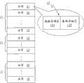
请参阅图1A及图1B其显示现有技艺的闪存的数据结构的示意图。图1A中,闪存1包含多个区块(block)11,且每一区块11包含多个分页(Page)12,而每一分页至少包含一区段(sector,亦称之为mini Page)13,区段13至少一数据存储区(data area)131及一备用存储区(space area)132。因标准的整合电子式驱动接口(Integrated Device Electronic,IDE-ATA)接口的传输最小单位为512字节(byte),因此数据存储区的存储空间一般为512字节,而备用存储区的存储空间为16字节。 Please refer to FIG. 1A and FIG. 1B , which are schematic diagrams showing the data structure of the prior art flash memory. In Fig. 1A, the flash memory 1 includes a plurality of blocks (block) 11, and each
请续参阅图1B,其显示现有技艺的备用存储区132的信息存储结构的示意图。图中,备用存储区132包含一存储器损坏信息141、一错误修正码检查信息142、一逻辑区块地址信息(logic block address,LBA)143、一分离区块逻辑区段地址信息(split blockl ogic sector address,SBLSA)144及一错误修正码(error correct code,ECC)的冗余码信息(redundant)145。Please continue to refer to FIG. 1B , which shows a schematic diagram of the information storage structure of the
上述提及的错误修正码大致可分为两类:一是区块码(Block Code)及另一是回旋码(Convolution Code)。所谓的区块码是将数据分成一个固定大小的区块来传送,其编码方法是对原始数据增加上冗余码信息,然后解码端在根据冗余码信息来作校正错误的动作。其中,区块码最常使用循环码分别为里德所罗门码(Reed-Solomon Code,RS)以及BCH(Bose ChaudhuriHocquengham)码。里德所罗门码的编解码均在有限场(Finite Field)GF(2m)中,m是正整数,有限场亦称为加洛瓦场(Galois Field,GF)。在此,里德所罗门码的编解码技术为此技术领域的工作者所熟知,在此不再赘述。 The error correction codes mentioned above can be roughly divided into two categories: one is the block code (Block Code) and the other is the convolution code (Convolution Code). The so-called block code is to divide the data into a block with a fixed size for transmission. The encoding method is to add redundant code information to the original data, and then the decoder performs error correction actions based on the redundant code information. Among them, the most commonly used cyclic codes of block codes are Reed-Solomon Code (Reed-Solomon Code, RS) and BCH (Bose Chaudhuri Hocquengham) code. The encoding and decoding of Reed-Solomon codes are all in the finite field (Finite Field) GF (2m ), m is a positive integer, and the finite field is also called Galois Field (Galois Field, GF). Here, the coding and decoding technology of the Reed-Solomon code is well known to workers in this technical field, and will not be repeated here.
当闪存以4位错误修正码进行编码,且所采用的里德所罗门码在GF(210)上时,产生的冗余码信息需要的存储空间为80位(10字节),即80=2×4×10。因此,在图1B所示的备用存储区132中,10字节保留为冗余码信息145的存储空间,其余6字节用以存储其它信息,存储器损坏信息141的存储空间为1字节,可包含一损坏区块信息(bad block,BS)及一损坏分页信息(badpage,PS),损坏区块信息用以标示此区块是否为一损坏区块,而损坏分页信息用以标示此分页是否为一损坏分页。错误修正码检查信息142的存储空间为1字节,用以标示是否须进行错误修正码确认。逻辑区块地址信息143的存储空间为2字节。分离区块逻辑区段地址信息144的存储空间为2字节。 When the flash memory is encoded with a 4-bit error correction code, and the adopted Reed-Solomon code is on GF(210 ), the storage space required for the generated redundant code information is 80 bits (10 bytes), that is, 80= 2×4×10. Therefore, in the
随着数据保护机制越来越受重视,用更高位错误修正码来进行编码是闪存的设计趋势,然而,若使用更高位错误修正码进行编码,例如6位错误修正码,且所采用的里德所罗门码在GF(210)上时,则产生的冗余码信息需要120位(15字节)的存储空间,120=2×6×10,而无法储入图1B所示的信息存储结构中。目前制造商根据现有的闪存结构通常都会为每一闪存配置有一定数量的额外存储空间,但由于这些额外的存储空间有限,无法扩增存储空间。因此,如何使闪存存储系统使用有限的存储空间来获取较佳的正确信息位亦是迫切需要的。 As the data protection mechanism is getting more and more attention, it is the design trend of flash memory to use higher bit error correction code for coding. However, if a higher bit error correction code is used for coding, such as 6 bit error correction code, and When the De-Solomon code is on GF(210 ), the generated redundant code information needs 120 bits (15 bytes) of storage space, 120=2×6×10, and cannot be stored in the information storage shown in Figure 1B in structure. At present, manufacturers usually configure a certain amount of additional storage space for each flash memory according to the existing flash memory structure, but because these additional storage spaces are limited, the storage space cannot be expanded. Therefore, how to make the flash storage system use the limited storage space to obtain better correct information bits is also urgently needed.
在现有技艺中,在信息存储结构里存储错误修正码检查信息142来标示此区段已写入数据或此区段为抹除后的区段。然而,存储错误修正码检查信息142需要一额外的空间,且位错误现象亦有可能发生在存储错误修正码检查信息的位,而造成解码过程的误判。因此,如何避免在闪存的区段进行解码时产生误判亦是迫切需要的。 In the prior art, the error correction code check information 142 is stored in the information storage structure to indicate that the segment has been written with data or the segment is an erased segment. However, storing the ECC checking information 142 requires an extra space, and bit errors may also occur in the bits storing the ECC checking information, resulting in misjudgment in the decoding process. Therefore, how to avoid misjudgment when decoding sectors of the flash memory is also urgently needed. the
发明内容Contents of the invention
因此本发明的目的为提供一适用于闪存的数据写入方法及其错误修正编解码方法,以在有限的存储器空间里提供安全性较好的数据保护机制。 Therefore, the purpose of the present invention is to provide a data writing method and an error correction encoding and decoding method suitable for flash memory, so as to provide a more secure data protection mechanism in a limited memory space. the
根据上述目的,本发明提供一种数据写入方法,用以将一数据写入一闪存的一区块的一区段,该区块由多个区段所组成,该数据包括多个字节数据(bytes),每一字节数据包含8个位,该方法包含:取得该区块的逻辑区块地址信息及一存储器损坏信息;调整该数据为多个编码组,每一编码组由9个位所组成;使用一6位错误修正码对该些编码组进行编码,以产生一冗余码信息,其中,该6位错误修正码采用由加洛瓦场GF(29)所产生的里德所罗门码(Reed-Solomon code);将该数据、该逻辑区块地址信息、该存储器损坏信息及该冗余码信息存储于该区段。 According to the above object, the present invention provides a data writing method for writing a data into a segment of a block of a flash memory, the block is composed of a plurality of segments, and the data includes a plurality of bytes Data (bytes), each byte of data includes 8 bits, the method includes: obtaining the logical block address information of the block and a memory damage information; adjusting the data into multiple code groups, each code group consists of 9 Composed of bits; use a 6-bit error correction code to encode these code groups to generate a redundant code information, wherein the 6-bit error correction code is generated by Galois field GF(29 ) Reed-Solomon code: storing the data, the logical block address information, the memory damage information and the redundancy code information in the segment.
藉由降低RS码的编解碼复杂度以减少冗余码的存储空间,而提高错误修正码的位数以提高数据安全性。 By reducing the encoding and decoding complexity of the RS code, the storage space of the redundant code is reduced, and the number of bits of the error correction code is increased to improve data security. the
此外,本发明更提供一适用于闪存的错误修正编码方法,用以对该闪存的一区块的一区段内所存储的数据进行编码,该区段包括一数据存储区、一参数信息存储区及一冗余码信息存储区,该编码方法包含:提供一抹除判断值,其与该数据存储区及该参数信息存储区的多个位皆为「0xff」的状态相关;取得欲存储于该数据存储区的一数据,使用该错误修正码对该数据进行编码,以产生一第二冗余码信息;将该第二冗余码信息与该抹除判断值进行一异或(XOR)逻辑运算,以产生一第三冗余码信息;将该数据及该第三冗余码信息分别存储于该数据存储区及该冗余码信息存储区。 In addition, the present invention further provides an error correction encoding method suitable for flash memory, which is used to encode data stored in a section of a block of the flash memory, and the section includes a data storage area, a parameter information storage area area and a redundant code information storage area, the encoding method includes: providing an erasure judgment value, which is related to the state that the multiple bits of the data storage area and the parameter information storage area are all "0xff"; A data in the data storage area is encoded by using the error correction code to generate a second redundant code information; an exclusive OR (XOR) is performed on the second redundant code information and the erasure judgment value Logic operation to generate a third redundancy code information; store the data and the third redundancy code information in the data storage area and the redundancy code information storage area respectively. the
再者,本发明再提供一适用于闪存的错误修正编码方法,用以对该闪存的一区块的一区段内所存储的数据进行解码,该区段包括一数据存储区、一参数信息存储区及一冗余码信息存储区,该数据存储区存储一数据,该冗余码信息存储区存储一第一冗余码信息,该错误修正解码方法包含:提供一抹除判断数值,其与该数据存储区及该参数信息存储区的多个位皆为「0xff」的状态相关;对将该第一冗余码信息与该抹除判断数值进行一异或(XOR)逻辑运算,以产生一第三冗余码信息;将该数据及该第三冗余码信息分别存储在该数据存储区及该冗余码信息存储区。 Moreover, the present invention further provides an error correction encoding method suitable for flash memory, used for decoding data stored in a section of a block of the flash memory, the section includes a data storage area, a parameter information A storage area and a redundant code information storage area, the data storage area stores a data, the redundant code information storage area stores a first redundant code information, the error correction decoding method includes: providing an erasure judgment value, which is consistent with A plurality of bits of the data storage area and the parameter information storage area are related to the state of "0xff"; an exclusive OR (XOR) logic operation is performed on the first redundancy code information and the erasure judgment value to generate A third redundancy code information; storing the data and the third redundancy code information in the data storage area and the redundancy code information storage area respectively. the
附图说明Description of drawings
为让本发明的上述和其它目的、特征、优点与实施例能更明显易懂,附图的详细说明如下: In order to make the above and other objects, features, advantages and embodiments of the present invention more obvious and understandable, the detailed description of the accompanying drawings is as follows:
图1A及图1B其显示现有技艺的闪存的数据结构的示意图; Fig. 1A and Fig. 1B it shows the schematic diagram of the data structure of the flash memory of prior art;
图2示出了本发明一实施例的数据写入方法的步骤流程图; Fig. 2 shows the flow chart of the steps of the data writing method of an embodiment of the present invention;
图3示出了本发明一实施例的闪存的区段的数据存储结构的示意图; Fig. 3 shows the schematic diagram of the data storage structure of the section of the flash memory of an embodiment of the present invention;
图4A示出了本发明一实施例的错误修正编码方法的步骤流程图; FIG. 4A shows a flow chart of steps of an error correction coding method according to an embodiment of the present invention;
图4B示出了本发明的抹除判断值的计算方法的步骤流程图;以及 Fig. 4B shows the step flow chart of the calculation method of erasing judgment value of the present invention; And
图5示出了本发明一实施例的错误修正解码方法的步骤流程图。 FIG. 5 shows a flowchart of steps of an error correction decoding method according to an embodiment of the present invention. the
附图符号说明 Description of reference symbols
1:闪存; 1: flash memory;
11:区块; 11: block;
12:分页; 12: pagination;
13:区段; 13: section;
131:数据存储区; 131: data storage area;
132:备用存储区; 132: backup storage area;
14:闪存; 14: flash memory;
141:存储器损坏信息; 141: Memory corruption information;
142:错误修正码检查信息; 142: error correction code check information;
143:逻辑区块地址信息; 143: logical block address information;
144:分离区块逻辑区段地址信息; 144: Separate block logic segment address information;
145:冗余码信息; 145: redundant code information;
21-24:步骤流程; 21-24: Step process;
30:区段; 30: section;
301:数据存储区; 301: data storage area;
302:前504个字节数据; 302: the first 504 bytes of data;
303:其余的8个字节数据; 303: the remaining 8 bytes of data;
304:备用存储区; 304: backup storage area;
305:参数信息存储区; 305: parameter information storage area;
306:冗余码信息存储区; 306: redundant code information storage area;
312,313:调整后的数据; 312, 313: adjusted data;
318:高位的位;318: high bit;
319:编码组; 319: encoding group;
41-44:步骤流程; 41-44: step process;
451-453:步骤流程;以及 451-453: Step Flow; and
51-53:步骤流程。 51-53: Step flow. the
具体实施方式Detailed ways
以下详细地讨论目前较佳的实施例。然而应被理解的是,本发明提供许多可适用的发明观念,而这些观念能被体现在很宽广多样的特定具体背景中。所讨论的特定具体的实施例仅是说明使用本发明的特定结构,而且不会限制本发明的范围。 The presently preferred embodiments are discussed in detail below. It should be appreciated, however, that the present invention provides many applicable inventive concepts that can be embodied in a wide variety of specific specific contexts. The specific specific embodiments discussed are merely illustrative of specific structures for using the invention, and do not limit the scope of the invention. the
请参阅图2及图3,图2示出了本发明一实施例的数据写入方法的步骤流程图,而图3示出了本发明一实施例的闪存的区段的数据存储结构的示意图。此方法用以将一数据写入一闪存的一区块的一区段,如图3所示,区段30包括一数据存储区301及一备用存储区304,数据存储区301的存储空间为512字节,而备用存区304的存储空间为16字节,每一字节数据309包含8个位,此方法包含下列步骤: Please refer to FIG. 2 and FIG. 3, FIG. 2 shows a flow chart of the steps of a data writing method according to an embodiment of the present invention, and FIG. 3 shows a schematic diagram of a data storage structure of a segment of a flash memory according to an embodiment of the present invention . This method is used to write a data into a section of a block of a flash memory, as shown in Figure 3, the
步骤21:取得包含此区段的区块的逻辑区块地址信息及一存储器损坏信息; Step 21: Obtain the logical block address information and a memory damage information of the block including this segment;
步骤22:将数据存储区301所存储的数据调整为多个编码组319,每一编码组319由9个位所组成;其中,前504个字节的数据302调整为448个编码组,如图3所示的数据312,而数据存储区301中其余的8个字节数据303则分别在高位318加入一位值为1的位,以形成8个编码组,如图3所示的数据313; Step 22: adjust the data stored in the
步骤23:使用一6位错误修正码对数据312及数据313所包含的编码组进行编码,以产生一冗余码信息,其中此6位错误修正码采用由加洛瓦场GF(29)所产生的里德所罗门码(Reed-Solomon code);其中,此冗余码信息所需的存储空间为108位,亦即,108=2×6×9; Step 23: Use a 6-bit error correction code to encode the code group contained in the
步骤24:将数据存储在数据存储区301中,而将逻辑区块地址信息、存储器损坏信息及冗余码信息存储在备用存区303中。 Step 24: Store data in the
在此实施例中,备用存区303包含参数信息存储区305及冗余码信息存储区306,参数信息存储区305包括2字节而冗余码信息存储区306包括14 字节,冗余码信息存储区306用以存储冗余码信息,而参数信息存储区305中的10位用以存储逻辑区块地址信息,5位用以存储存储器损坏信息,而1位可用以存储分离区块逻辑区段地址信息或存储其它信息。 In this embodiment, the
此外,如为了加强数据安全性,在进行步骤32的调整动作时,亦可将存储在区域305的数据一起调整,并在进行步骤33的编码动作时,与数据312及数据313一起编码。 In addition, in order to enhance data security, the data stored in the
对闪存的区段进行解码时,存储数据的区段包含下列三种状态: When decoding a segment of flash memory, a segment storing data contains the following three states:
(1)此区段已写入数据,且数据可完成解码,可读出正确数据。 (1) Data has been written in this segment, and the data can be decoded and correct data can be read out. the
(2)此区段已写入数据,然数据无法完成解码,无法顺利读出数据。 (2) Data has been written in this segment, but the data cannot be decoded, and the data cannot be read out smoothly. the
(3)此区段为抹除(erase)后的区段,未写入数据。 (3) This segment is the segment after erasing (erase), and no data has been written. the
由于经过抹除后的存储器存储器储的数据全为「0xff」,若是以错误修正码对全为「0xff」的数据进行解码,则会发生解码错误,而容易造成状态(2)及状态(3)的误判。当区段被判断为状态(2)时,系统会将其视为坏轨,之后不再使用此区段来。在没有多余的空间可存储一用以标示状态(2)或状态(3)的数据的情况下,本发明提出一种错误修正编码方法,可不需存储多余的标示数据并避免状态(2)或状态(3)的误判。 Since the data stored in the erased memory is all "0xff", if the error correction code is used to decode the data that is all "0xff", a decoding error will occur, and it is easy to cause state (2) and state (3) ) misjudgment. When a section is judged as status (2), the system will regard it as a bad track, and this section will no longer be used. In the case that there is no extra space to store a data used to mark state (2) or state (3), the present invention proposes an error correction coding method, which does not need to store redundant mark data and avoids state (2) or state (3). Misjudgment of state (3). the
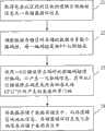
请参阅图4A,其显示本发明一实施例的错误修正编码方法的步骤流程图。此方法用以对闪存的一区块的一区段内所存储的数据进行编码,如图3所示,此区段包括一数据存储区301、一参数信息存储区305及一冗余码信息存储区306,此方法包含下列步骤: Please refer to FIG. 4A , which shows a flowchart of steps of an error correction encoding method according to an embodiment of the present invention. This method is used to encode the data stored in a section of a block of flash memory, as shown in Figure 3, this section includes a
步骤41:提供一抹除判断值,其与该数据存储区及该参数信息存储区的多个位皆为「0xff」的状态相关; Step 41: Provide an erasing judgment value, which is related to the state that multiple bits of the data storage area and the parameter information storage area are all "0xff";
步骤42:取得欲存储在数据存储区301的一数据,使用上述的错误修正码对此数据进行编码,以产生一第二冗余码信息; Step 42: Obtain a data to be stored in the
步骤43:将第二冗余码信息与此抹除判断值进行一异或(XOR)逻辑运算,以产生一第三冗余码信息;以及 Step 43: Perform an exclusive OR (XOR) logical operation on the second redundant code information and the erasure judgment value to generate a third redundant code information; and
步骤44:将数据及第三冗余码信息分别存储在数据存储区301及冗余码信息存储区306。 Step 44: Store the data and the third redundancy code information in the
请续参阅图4B,其绘示本发明的抹除判断值的计算方法的实施例。图中,此计算方法对应于图3,此计算方法包含下列步骤: Please continue to refer to FIG. 4B , which illustrates an embodiment of the calculation method of the erasure judgment value of the present invention. In the figure, this calculation method corresponds to Figure 3, and this calculation method includes the following steps:
步骤451:提供一与数据存储区301及参数信息存储区305的存储空间 大小相同的多个字节,并将此些字节设定为「0xff」; Step 451: Provide a plurality of bytes with the same size as the storage space of the
步骤452:使用一错误修正码(ECC)对此些字节进行编码,以产生一第一冗余码信息; Step 452: use an error correction code (ECC) to encode these bytes to generate a first redundant code information;
步骤453:计算此第一冗余码信息的一补码(complement),以此补码作为此抹除判断值。 Step 453: Calculate a complement of the first redundant code information, and use the complement as the erasure judgment value. the
在此计算方法中,抹除判断值仅与错误修正码、数据存储区及参数信息存储区的存储空间相关,因此,若上述条件不变的话,抹除判断值可先预先计算好,而执行错误修正编码方法时便使用此预先算好的抹除判断值来编码。若上述条件会变动的话,则每次进行错误修正编码方法时便执行步骤451到步骤453,以计算抹除判断值。 In this calculation method, the erasure judgment value is only related to the storage space of the error correction code, data storage area, and parameter information storage area. Therefore, if the above conditions remain unchanged, the erasure judgment value can be pre-calculated and executed. The pre-calculated erasure judgment value is used for encoding in the error correction encoding method. If the above conditions will change, step 451 to step 453 are executed each time the error correction encoding method is performed to calculate the erasure judgment value. the
如果要从闪存的一区块读取数据,必须先对区块内的数据进行错误修正码解码程序,方能确定数据的正确性。如果此区块为一抹除区块,则区块内的数据皆为「0xff」,若以此数据进行错误修正码解码程序,会造成解码失败,造成上述状态(2)或状态(3)的误判。以下便是本发明所提出可避免此种情况的方法。 If you want to read data from a block of flash memory, you must first perform an error correction code decoding program on the data in the block to determine the correctness of the data. If this block is an erasing block, the data in the block is all "0xff". If the error correction code decoding process is performed on this data, the decoding will fail, resulting in the above state (2) or state (3). Misjudgment. The following is the method proposed by the present invention to avoid this situation. the
请参阅图5,其显示本发明一实施例的错误修正解码方法的步骤流程图。此方法用以对闪存的一区块的一区段内所存储的数据进行解码,如图3所示,区段3包括一数据存储区301、一参数信息存储区305及一冗余码信息存储区306,数据存储区301存储一数据,而冗余码信息存储区306存储一第四冗余码信息。此方法包含下列步骤: Please refer to FIG. 5 , which shows a flowchart of steps of an error correction decoding method according to an embodiment of the present invention. This method is used to decode the data stored in a section of a block of flash memory, as shown in Figure 3, section 3 includes a
步骤51:提供一抹除判断数值,其与数据存储区301及参数信息存储区305的多个位皆为「0xff」的状态相关; Step 51: Provide an erasing judgment value, which is related to the state that a plurality of bits in the
步骤52:对将第四冗余码信息与抹除判断数值进行一异或(XOR)逻辑运算,以产生一第五冗余码信息;以及 Step 52: Perform an exclusive OR (XOR) logical operation on the fourth redundant code information and the erasure judgment value to generate a fifth redundant code information; and
步骤53:根据第五冗余码信息对存储在数据存储区301的数据进行一错误修正码解码程序。 Step 53: Perform an ECC decoding process on the data stored in the
其中,抹除判断数值可使用图4B所示的计算方法来计算出。在此计算方法中,抹除判断值仅与错误修正码、数据存储区及参数信息存储区的存储空间相关,因此,若上述条件不变的话,抹除判断值可先预先计算好,而执行错误修正解码方法时便使用此预先算好的抹除判断值来编码。若上述条件会变动的话,则每次进行错误修正解码方法时便执行步骤451到步骤453,以 计算抹除判断值。 Wherein, the erasure determination value can be calculated using the calculation method shown in FIG. 4B. In this calculation method, the erasure judgment value is only related to the storage space of the error correction code, data storage area, and parameter information storage area. Therefore, if the above conditions remain unchanged, the erasure judgment value can be pre-calculated and executed. The pre-calculated erasure judgment value is used for encoding in the error correction decoding method. If above-mentioned conditions can change, then just execute
在上述解码过程中,若数据存储区301及参数信息存储区305里存储的是真正经过编码的数据以其编码所产生的冗余码信息,由于编码时这些数据已经与抹除判断数值进行过一次XOR运算,因此在步骤52时再经过一次XOR运算会得到原始的已编码的数据以其编码所产生的冗余码信息,其可完成步骤53所执行的一错误修正码解码程序。 In the above-mentioned decoding process, if the data stored in the
若在解码时,数据存储区301及参数信息存储区305里存储的全是「0xff」,经过步骤52处理后,经处理的数据存储区301及参数信息存储区305里的数据便可完成错误修正码解码程序,且解码出来的数据全为「0xff」,固可以判断此区段为抹除后的区段。藉由上述错误修正编解码方法,参数信息存储区305中便不需再存储一错误修正码检查信息,可减少所需的存储空间。 If when decoding, the
上述闪存可为多级单元(Multi Level Cell,MLC)及单级单元(SingleLevel Cell,SLC)两种其中之一。 The above-mentioned flash memory can be one of two types: multi-level cell (Multi Level Cell, MLC) and single-level cell (Single Level Cell, SLC). the
虽然本发明已以较佳实施例揭露如上,然其并非用以限定本发明,任何熟习此技艺者,在不脱离本发明的精神和范围内,当可作各种的更动与润饰,因此本发明的保护范围当视本发明申请专利范围所界定者为准。Although the present invention has been disclosed above with preferred embodiments, it is not intended to limit the present invention. Any person skilled in the art can make various changes and modifications without departing from the spirit and scope of the present invention. Therefore The scope of protection of the present invention should be defined by the patent scope of the present invention.
Claims (4)
Translated fromChinesePriority Applications (1)
| Application Number | Priority Date | Filing Date | Title |
|---|---|---|---|
| CN200710103472XACN101308706B (en) | 2007-05-18 | 2007-05-18 | Data writing method and error correction encoding/decoding method suitable for flash memory |
Applications Claiming Priority (1)
| Application Number | Priority Date | Filing Date | Title |
|---|---|---|---|
| CN200710103472XACN101308706B (en) | 2007-05-18 | 2007-05-18 | Data writing method and error correction encoding/decoding method suitable for flash memory |
Publications (2)
| Publication Number | Publication Date |
|---|---|
| CN101308706A CN101308706A (en) | 2008-11-19 |
| CN101308706Btrue CN101308706B (en) | 2012-01-04 |
Family
ID=40125090
Family Applications (1)
| Application Number | Title | Priority Date | Filing Date |
|---|---|---|---|
| CN200710103472XAActiveCN101308706B (en) | 2007-05-18 | 2007-05-18 | Data writing method and error correction encoding/decoding method suitable for flash memory |
Country Status (1)
| Country | Link |
|---|---|
| CN (1) | CN101308706B (en) |
Families Citing this family (7)
| Publication number | Priority date | Publication date | Assignee | Title |
|---|---|---|---|---|
| KR102285940B1 (en) | 2015-05-29 | 2021-08-05 | 에스케이하이닉스 주식회사 | Data processing circuit, data storage device comprising data processing circuit and operating method thereof |
| US11515897B2 (en) | 2015-05-29 | 2022-11-29 | SK Hynix Inc. | Data storage device |
| US11177835B2 (en) | 2015-09-25 | 2021-11-16 | SK Hynix Inc. | Data storage device |
| US11611359B2 (en) | 2015-05-29 | 2023-03-21 | SK Hynix Inc. | Data storage device |
| US10396827B2 (en) | 2015-09-25 | 2019-08-27 | SK Hynix Inc. | Data storage device |
| KR102347418B1 (en)* | 2015-09-25 | 2022-01-06 | 에스케이하이닉스 주식회사 | Data processing device and operating method thereof |
| CN107562563B (en)* | 2016-07-01 | 2021-06-15 | 龙芯中科技术股份有限公司 | Nand Flash control method and device |
Citations (3)
| Publication number | Priority date | Publication date | Assignee | Title |
|---|---|---|---|---|
| US5951708A (en)* | 1995-05-30 | 1999-09-14 | Mitsubishi Denki Kabushiki Kaisha | Error correction coding and decoding method, and circuit using said method |
| CN1518696A (en)* | 2001-06-21 | 2004-08-04 | 皇家菲利浦电子有限公司 | Memory error handling method and circuit arrangement |
| CN1849750A (en)* | 2004-01-15 | 2006-10-18 | 桑德布里奇技术公司 | A method of reed-solomon encoding and decoding |
- 2007
- 2007-05-18CNCN200710103472XApatent/CN101308706B/enactiveActive
Patent Citations (3)
| Publication number | Priority date | Publication date | Assignee | Title |
|---|---|---|---|---|
| US5951708A (en)* | 1995-05-30 | 1999-09-14 | Mitsubishi Denki Kabushiki Kaisha | Error correction coding and decoding method, and circuit using said method |
| CN1518696A (en)* | 2001-06-21 | 2004-08-04 | 皇家菲利浦电子有限公司 | Memory error handling method and circuit arrangement |
| CN1849750A (en)* | 2004-01-15 | 2006-10-18 | 桑德布里奇技术公司 | A method of reed-solomon encoding and decoding |
Also Published As
| Publication number | Publication date |
|---|---|
| CN101308706A (en) | 2008-11-19 |
Similar Documents
| Publication | Publication Date | Title |
|---|---|---|
| KR101588605B1 (en) | Memory controller supporting rate compatible punctured codes | |
| US8055983B2 (en) | Data writing method for flash memory and error correction encoding/decoding method thereof | |
| US8239725B2 (en) | Data storage with an outer block code and a stream-based inner code | |
| TWI385666B (en) | Data structure for flash memory and data reading/writing method thereof | |
| TWI594254B (en) | Method for reading data from block of flash memory and associated memory device | |
| US9037951B2 (en) | Data management in solid state storage systems | |
| US9543983B2 (en) | Decoding method, memory storage device and memory control circuit unit | |
| US8321757B2 (en) | Method and apparatus for error correction | |
| CN105051700B (en) | Select redundant storage configuration based on available storage space | |
| CN101308706B (en) | Data writing method and error correction encoding/decoding method suitable for flash memory | |
| CN104733051B (en) | Decoding method of parity check code, memory storage device and control circuit unit | |
| CN106297883B (en) | Decoding method, memory storage device, and memory control circuit unit | |
| TWI628543B (en) | Decoding method, memory storage device and memory control circuit unit | |
| TWI536749B (en) | Decoding method, memory storage device and memory controlling circuit unit | |
| CN101308702A (en) | Data structure suitable for flash memory and data writing method and data reading method thereof | |
| CN112051963A (en) | Data writing method, memory control circuit unit and memory storage device | |
| CN105304143B (en) | Decoding method, memory control circuit unit and memory storage device | |
| CN112799874B (en) | Memory control method, memory storage device and memory control circuit unit | |
| CN117409845A (en) | Packet management method, memory storage device and memory controller | |
| CN108170554B (en) | NAND data coding method and device | |
| CN117632579B (en) | Memory control method and memory storage device | |
| TWI777087B (en) | Data managing method, memory controlling circuit unit and memory storage device | |
| CN117785545A (en) | Decoding method, memory storage device and memory control circuit unit | |
| CN107301873A (en) | Decoding method, memory storage device and memory control circuit unit | |
| TW202530987A (en) | Memory control method and memory storage device |
Legal Events
| Date | Code | Title | Description |
|---|---|---|---|
| C06 | Publication | ||
| PB01 | Publication | ||
| C10 | Entry into substantive examination | ||
| SE01 | Entry into force of request for substantive examination | ||
| C14 | Grant of patent or utility model | ||
| GR01 | Patent grant |