CN101308309B - Electronic ink display panel - Google Patents
Electronic ink display panelDownload PDFInfo
- Publication number
- CN101308309B CN101308309BCN2007101070285ACN200710107028ACN101308309BCN 101308309 BCN101308309 BCN 101308309BCN 2007101070285 ACN2007101070285 ACN 2007101070285ACN 200710107028 ACN200710107028 ACN 200710107028ACN 101308309 BCN101308309 BCN 101308309B
- Authority
- CN
- China
- Prior art keywords
- electronic ink
- display panel
- material pattern
- pixel
- ink display
- Prior art date
- Legal status (The legal status is an assumption and is not a legal conclusion. Google has not performed a legal analysis and makes no representation as to the accuracy of the status listed.)
- Active
Links
Images


Landscapes
- Electrochromic Elements, Electrophoresis, Or Variable Reflection Or Absorption Elements (AREA)
Abstract
Description
Translated fromChinese技术领域technical field
本发明涉及一种显示面板,且尤其涉及一种电子墨水显示面板(electronic-ink display panel)。The present invention relates to a display panel, and in particular to an electronic-ink display panel.
背景技术Background technique
一般而言,目前常见的电子墨水显示装置包括一前盖板(front planelaminate,FPL)、一电子墨水层以及一薄膜晶体管阵列基板(thin filmtransistor array substrate),其中前盖板具有一透明电极层;电子墨水层具有以带电粒子作动并具有双稳态(Bi-Stable)的显示材料(即电子墨水)。Generally speaking, the current common electronic ink display device includes a front plane laminate (FPL), an electronic ink layer and a thin film transistor array substrate (thin film transistor array substrate), wherein the front plane has a transparent electrode layer; The electronic ink layer has a bi-stable (Bi-Stable) display material (ie, electronic ink) that acts as charged particles.
以一现有技术的电子墨水层为例:带电粒子为颜色不同的正电荷和负电荷(例如:黑色和白色)且带电粒子与一透明流体包含于一微胶囊中。当薄膜晶体管阵列基板的各像素电极与透明电极层之间的电场改变时,不同颜色的正电荷和负电荷便会根据电场方向而向上或向下移动,进而使各微胶囊呈现出黑色或白色。另外,微胶囊也可包含有颜色不同的单一电荷和不透明流体(例如:黑色和白色)。薄膜晶体管阵列基板的各像素电极与透明电极层之间的电场改变时,带电粒子中的单一电荷便会根据电场方向而向上或向下移动,而集中在微胶囊中的某一面,使各微胶囊呈现出黑色或白色。Taking a prior art electronic ink layer as an example: the charged particles are positively charged and negatively charged in different colors (eg black and white) and the charged particles are contained in a microcapsule with a transparent fluid. When the electric field between each pixel electrode of the thin film transistor array substrate and the transparent electrode layer changes, the positive and negative charges of different colors will move up or down according to the direction of the electric field, thereby making each microcapsule appear black or white . In addition, microcapsules can also contain single charges and opaque fluids of different colors (eg black and white). When the electric field between each pixel electrode of the thin film transistor array substrate and the transparent electrode layer changes, the single charges in the charged particles will move up or down according to the direction of the electric field, and concentrate on one side of the microcapsules, making each microcapsule Capsules appear black or white.
以再一现有技术的电子墨水层为例,带电粒子为表面具有二种不同颜色(例如:黑色和白色)的双色带电粒子,且双色带电粒子的表面根据表面颜色,而具有不同的电荷。当薄膜晶体管阵列基板的各像素电极与透明电极层之间的电场改变时,此双色带电粒子便会根据电场方向而滚动,进而使各带电粒子呈现出黑色或白色。Taking another electronic ink layer in the prior art as an example, the charged particles are two-color charged particles with two different colors (eg, black and white) on the surface, and the surfaces of the two-color charged particles have different charges according to the surface colors. When the electric field between each pixel electrode of the thin film transistor array substrate and the transparent electrode layer changes, the two-color charged particles will roll according to the direction of the electric field, so that each charged particle appears black or white.
图1A为现有技术的一电子墨水显示面板的结构示意图,图1B为图1A中的电子墨水显示面板的薄膜晶体管阵列基板的俯视图,其中图1A的电子墨水显示面板的薄膜晶体管阵列基板是沿着图1B中的剖面线A-A’的剖面图。请同时参照图1A与图1B,电子墨水显示面板10包括一薄膜晶体管阵列基板20、一前盖板30以及一电子墨水层40。其中,前盖板30配置于薄膜晶体管阵列基板20的上方。电子墨水层40配置于前盖板30与薄膜晶体管阵列基板20之间。Fig. 1A is a schematic structural view of an electronic ink display panel in the prior art, and Fig. 1B is a top view of the thin film transistor array substrate of the electronic ink display panel in Fig. 1A, wherein the thin film transistor array substrate of the electronic ink display panel in Fig. 1A is along the Follow the sectional view of the section line AA' in Fig. 1B. Please refer to FIG. 1A and FIG. 1B at the same time. The electronic
薄膜晶体管阵列基板20包括一基板21、多条扫描线22、多条数据线23以及多个次像素单元24。其中,扫描线22、数据线23配置于基板21上,并于基板21上定义多个像素区域21a。次像素单元24分别配置基板21上的像素区域21a中,且每一次像素单元24具有一储存电容24a。此外,每一次像素单元24还具有一薄膜晶体管24b以及一像素电极24c。薄膜晶体管24b与其中一条扫描线22及其中一条数据线23电性相连。像素电极24c则与薄膜晶体管24b电性相连。前盖板30包括一保护膜32以及一透明电极层34。透明电极层34配置于保护膜32上。The
承上述,通过在扫描线22、数据线23以及透明电极层34上施加适当的电压信号,使像素电极24c充放电。如此,电子墨水材料层40中的微胶囊41的带有颜色的电荷便会被驱动,电子墨水显示装置10便可显示画面。上述的电子墨水显示装置10只能显示黑白的画面。然而,目前显示装置的彩色化已经成为必然的趋势,若电子墨水显示装置10仅能显示出黑白的画面,其应用层面将有所限制。Based on the above, by applying appropriate voltage signals to the
图1C为又一现有技术的电子墨水显示面板42的结构示意图,电子墨水显示面板42类似于电子墨水显示面板10,但不同之处为:电子墨水显示面板42的电子墨水层40使用双色带电粒子44来取代图1A所示的微胶囊41。FIG. 1C is a schematic structural view of another electronic
图1D为再一现有技术的电子墨水显示面板45的结构示意图,电子墨水显示面板45类似于电子墨水显示面板10,但不同之处为:电子墨水显示面板45的电子墨水层40的微胶囊41包含不透明流体46(例如:白色)和单一带电粒子47(例如黑色)。带电粒子47可根据电场方向来上下移动,若带电粒子47往上移动,电子墨水显示面板45即显示黑色,若带电粒子47往下移动,电子墨水显示面板45则显示白色。1D is a schematic structural view of another electronic
发明内容Contents of the invention
本发明所要解决的技术问题在于提供一种能显示彩色画面的电子墨水显示面板,其具有多个次像素单元,且每一次像素单元的总电容值(储存电容器与显示电容器的电容总和)都相等。The technical problem to be solved by the present invention is to provide an electronic ink display panel capable of displaying color pictures, which has a plurality of sub-pixel units, and the total capacitance value of each sub-pixel unit (the sum of the capacitance of the storage capacitor and the display capacitor) is equal .
为实现上述或是其它目的,本发明提供一种电子墨水显示面板,此电子墨水显示面板包括一主动元件阵列基板、一前盖板以及一电子墨水层。主动元件阵列基板具有多个像素单元,其中每一像素单元包括多个次像素单元,而每一次像素单元具有一储存电容器。在同一像素单元中,至少有其中一个次像素单元的储存电容器的电容值与其它次像素单元的储存电容器的电容值不同。前盖板配置于主动元件阵列基板上方。电子墨水层配置于主动元件阵列基板与前盖板之间。To achieve the above or other objectives, the present invention provides an electronic ink display panel, which includes an active device array substrate, a front cover and an electronic ink layer. The active device array substrate has a plurality of pixel units, wherein each pixel unit includes a plurality of sub-pixel units, and each sub-pixel unit has a storage capacitor. In the same pixel unit, the capacitance value of the storage capacitor of at least one sub-pixel unit is different from that of the storage capacitors of other sub-pixel units. The front cover is disposed above the active element array substrate. The electronic ink layer is disposed between the active device array substrate and the front cover.
依照本发明一实施例所述的电子墨水显示面板,前述的主动元件阵列基板还包括一基板、多条扫描线以及多条数据线。扫描线与数据线都配置于基板上,其中扫描线与数据线于基板上定义出多个像素区域。According to an electronic ink display panel according to an embodiment of the present invention, the aforementioned active device array substrate further includes a substrate, a plurality of scanning lines and a plurality of data lines. Both the scan lines and the data lines are configured on the substrate, wherein the scan lines and the data lines define a plurality of pixel regions on the substrate.
依照本发明一实施例所述的电子墨水显示面板,前述的每一像素单元包括一第一次像素单元、一第二次像素单元以及一第三次像素单元。第一次像素单元具有一第一储存电容器。第二次像素单元具有一第二储存电容器。第三次像素单元具有一第三储存电容器。其中,每一像素单元的第一次像素单元、第二次像素单元以及第三次像素单元与同一扫描线电性连接,且分别位于并排设置的三个像素区域中。According to an electronic ink display panel according to an embodiment of the present invention, each of the aforementioned pixel units includes a first sub-pixel unit, a second sub-pixel unit and a third sub-pixel unit. The first pixel unit has a first storage capacitor. The second sub-pixel unit has a second storage capacitor. The third sub-pixel unit has a third storage capacitor. Wherein, the first sub-pixel unit, the second sub-pixel unit and the third sub-pixel unit of each pixel unit are electrically connected to the same scanning line, and are respectively located in three pixel regions arranged side by side.
依照本发明一实施例所述的电子墨水显示面板,前述的前盖板包括一共享电极以及一保护膜。共享电极配置于电子墨水层上。保护膜配置于共享电极上。According to an embodiment of the electronic ink display panel of the present invention, the aforementioned front cover includes a shared electrode and a protective film. The shared electrode is configured on the electronic ink layer. The protective film is disposed on the common electrode.
依照本发明一实施例所述的电子墨水显示面板,前述的每一第一次像素单元具有一第一主动元件以及一与第一主动元件电性连接的第一像素电极。前述的每一第二次像素单元具有一第二主动元件以及一与第二主动元件电性连接的第二像素电极。前述的每一第三次像素单元具有一第三主动元件以及一与第三主动元件电性连接的第三像素电极。According to the electronic ink display panel according to an embodiment of the present invention, each of the aforementioned first pixel units has a first active element and a first pixel electrode electrically connected to the first active element. Each of the aforementioned second sub-pixel units has a second active element and a second pixel electrode electrically connected to the second active element. Each of the aforementioned third sub-pixel units has a third active element and a third pixel electrode electrically connected to the third active element.
依照本发明一实施例所述的电子墨水显示面板,前述的电子墨水层包括多个第一墨水材料图案、多个第二墨水材料图案以及多个第三墨水材料图案。第一墨水材料图案配置于第一像素电极上。第二墨水材料图案配置于第二像素电极上。第三墨水材料图案配置于第三次像素电极上。According to the electronic ink display panel according to an embodiment of the present invention, the aforementioned electronic ink layer includes a plurality of first ink material patterns, a plurality of second ink material patterns and a plurality of third ink material patterns. The first ink material pattern is configured on the first pixel electrode. The second ink material pattern is configured on the second pixel electrode. The third ink material pattern is configured on the third sub-pixel electrode.
依照本发明一实施例所述的电子墨水显示面板,前述的第一储存电容器的电容值为C1,前述的第二储存电容器的电容值为C2,而前述的第三储存电容器的电容值为C3,且C1≠C2≠C3。According to the electronic ink display panel according to an embodiment of the present invention, the capacitance value of the first storage capacitor is C1, the capacitance value of the second storage capacitor is C2, and the capacitance value of the third storage capacitor is C3 , and C1≠C2≠C3.
依照本发明一实施例所述的电子墨水显示面板,前述的共享电极、其中一第一墨水材料图案以及对应的第一像素电极所构成的电容器的电容值为Ce1,前述的共享电极、其中一第二墨水材料图案以及对应的第二像素电极所构成的电容器的电容值为Ce2,前述的共享电极、其中一第三墨水材料图案以及对应的第三像素电极所构成的电容器的电容值为Ce3,而Ce1≠Ce2≠Ce3,且C1+Ce1=C2+Ce2=C3+Ce3。According to an electronic ink display panel according to an embodiment of the present invention, the capacitance value of the capacitor formed by the aforementioned shared electrode, one of the first ink material patterns, and the corresponding first pixel electrode is Ce1, and the aforementioned shared electrode, one of the The capacitance value of the capacitor formed by the second ink material pattern and the corresponding second pixel electrode is Ce2, and the capacitance value of the capacitor formed by the aforementioned shared electrode, one of the third ink material patterns and the corresponding third pixel electrode is Ce3 , and Ce1≠Ce2≠Ce3, and C1+Ce1=C2+Ce2=C3+Ce3.
依照本发明一实施例所述的电子墨水显示面板,前述的第一储存电容器所占据的面积为A1,前述的第二储存电容器所占据的面积为A2,而前述的第三储存电容器所占据的面积为A3,且A1≠A2≠A3。According to the electronic ink display panel according to an embodiment of the present invention, the area occupied by the aforementioned first storage capacitor is A1, the area occupied by the aforementioned second storage capacitor is A2, and the area occupied by the aforementioned third storage capacitor is The area is A3, and A1≠A2≠A3.
依照本发明一实施例所述的电子墨水显示面板,前述的第一墨水材料图案的厚度为d1,前述的第二墨水材料图案的厚度为d2,而前述的第三墨水材料图案的厚度为d3,且d1≠d2≠d3。According to an electronic ink display panel according to an embodiment of the present invention, the thickness of the aforementioned first ink material pattern is d1, the thickness of the aforementioned second ink material pattern is d2, and the thickness of the aforementioned third ink material pattern is d3 , and d1≠d2≠d3.
依照本发明一实施例所述的电子墨水显示面板,前述的第一墨水材料图案、前述的第二墨水材料图案、前述的第三墨水材料图案的材质不同。According to the electronic ink display panel according to an embodiment of the present invention, the materials of the aforementioned first ink material pattern, the aforementioned second ink material pattern, and the aforementioned third ink material pattern are different.
依照本发明一实施例所述的电子墨水显示面板,前述的共享电极与每一第一像素电极重迭的面积为B1,前述的共享电极与每一第二像素电极重迭的面积为B2,前述的共享电极与每一第三像素电极重迭的面积为B3,而B1≠B2≠B3。According to an electronic ink display panel according to an embodiment of the present invention, the overlapping area of the aforementioned shared electrode and each first pixel electrode is B1, and the overlapping area of the aforementioned shared electrode and each second pixel electrode is B2, The overlapping area of the aforementioned shared electrode and each third pixel electrode is B3, and B1≠B2≠B3.
依照本发明一实施例所述的电子墨水显示面板,前述的第一储存电容器的电容值为C1,前述的第二储存电容器的电容值为C2,前述的第三储存电容器的电容值为C3,且C1≠C2,C2=C3。According to the electronic ink display panel according to an embodiment of the present invention, the capacitance value of the aforementioned first storage capacitor is C1, the aforementioned second storage capacitor has a capacitance value of C2, and the aforementioned third storage capacitor has a capacitance value of C3, And C1≠C2, C2=C3.
依照本发明一实施例所述的电子墨水显示面板,前述的共享电极、其中一第一墨水材料图案以及对应的第一像素电极所构成的电容器的电容值为Ce1,前述的共享电极、其中一第二墨水材料图案以及对应的第二像素电极所构成的电容器的电容值为Ce2,前述的共享电极、其中一第三墨水材料图案以及对应的第三像素电极所构成的电容器的电容值为Ce3,且Ce1≠Ce2,而Ce2=Ce3。According to an electronic ink display panel according to an embodiment of the present invention, the capacitance value of the capacitor formed by the aforementioned shared electrode, one of the first ink material patterns, and the corresponding first pixel electrode is Ce1, and the aforementioned shared electrode, one of the The capacitance value of the capacitor formed by the second ink material pattern and the corresponding second pixel electrode is Ce2, and the capacitance value of the capacitor formed by the aforementioned shared electrode, one of the third ink material patterns and the corresponding third pixel electrode is Ce3 , and Ce1≠Ce2, and Ce2=Ce3.
依照本发明一实施例所述的电子墨水显示面板,前述的第一储存电容器所占据的面积为A1,前述的第二储存电容器所占据的面积为A2,而前述的第三储存电容器所占据的面积为A3,且A1≠A2,A2=A3。According to the electronic ink display panel according to an embodiment of the present invention, the area occupied by the aforementioned first storage capacitor is A1, the area occupied by the aforementioned second storage capacitor is A2, and the area occupied by the aforementioned third storage capacitor is The area is A3, and A1≠A2, A2=A3.
依照本发明一实施例所述的电子墨水显示面板,前述的第一墨水材料图案的厚度为d1,前述的第二墨水材料图案的厚度为d2,且前述的第三墨水材料图案的厚度为d3,而d1≠d2,d2=d3。According to the electronic ink display panel according to an embodiment of the present invention, the thickness of the aforementioned first ink material pattern is d1, the thickness of the aforementioned second ink material pattern is d2, and the thickness of the aforementioned third ink material pattern is d3 , and d1≠d2, d2=d3.
依照本发明一实施例所述的电子墨水显示面板,前述的第一墨水材料图案、前述的第二墨水材料图案的材质不同,前述的第二墨水材料图案与前述的第三墨水材料图案的材质相同。According to the electronic ink display panel according to an embodiment of the present invention, the materials of the aforementioned first ink material pattern and the aforementioned second ink material pattern are different, and the materials of the aforementioned second ink material pattern and the aforementioned third ink material pattern same.
依照本发明一实施例所述的电子墨水显示面板,前述的共享电极与每一第一像素电极重迭的面积为B1,前述的共享电极与每一第二像素电极重迭的面积为B2,前述的共享电极与每一第三像素电极重迭的面积为B3,而B1≠B2,B2=B3。According to an electronic ink display panel according to an embodiment of the present invention, the overlapping area of the aforementioned shared electrode and each first pixel electrode is B1, and the overlapping area of the aforementioned shared electrode and each second pixel electrode is B2, The overlapping area of the aforementioned common electrode and each third pixel electrode is B3, and B1≠B2, B2=B3.
依照本发明一实施例所述的电子墨水显示面板,前述的第一墨水材料图案包括多个微胶囊,每一微胶囊中包括多个第一粒子、多个第二粒子以及一透明流体。其中,第一粒子与第二粒子分布于透明流体中,且各自带有不同的电性。According to the electronic ink display panel according to an embodiment of the present invention, the aforementioned first ink material pattern includes a plurality of microcapsules, and each microcapsule includes a plurality of first particles, a plurality of second particles and a transparent fluid. Wherein, the first particles and the second particles are distributed in the transparent fluid, and each has different electrical properties.
依照本发明一实施例所述的电子墨水显示面板,前述的第二墨水材料图案包括多个微胶囊,每一微胶囊中包括多个第三粒子、多个第四粒子以及一透明流体。其中,第三粒子与第四粒子分布于透明流体中,且各自带有不同的电性。According to the electronic ink display panel according to an embodiment of the present invention, the aforementioned second ink material pattern includes a plurality of microcapsules, and each microcapsule includes a plurality of third particles, a plurality of fourth particles and a transparent fluid. Wherein, the third particle and the fourth particle are distributed in the transparent fluid, and each has different electrical properties.
依照本发明一实施例所述的电子墨水显示面板,前述的第三墨水材料图案包括多个微胶囊,每一微胶囊中包括多个第五粒子、多个第六粒子以及一透明流体。其中,第五粒子与第六粒子分布于透明流体中,且各自带有不同的电性。According to the electronic ink display panel according to an embodiment of the present invention, the aforementioned third ink material pattern includes a plurality of microcapsules, and each microcapsule includes a plurality of fifth particles, a plurality of sixth particles and a transparent fluid. Wherein, the fifth particle and the sixth particle are distributed in the transparent fluid, and each has different electrical properties.
依照本发明一实施例所述的电子墨水显示面板,前述的第一墨水材料图案包括多个双色带电粒子,每一双色带电粒子的一表面布满多个第一粒子,而每一双色带电粒子的另一表面布满多个第二粒子,其中第一粒子与第二粒子各自带有不同的电性。According to the electronic ink display panel described in an embodiment of the present invention, the aforesaid first ink material pattern includes a plurality of charged particles of two colors, one surface of each charged particle of two colors is covered with a plurality of first particles, and each charged particle of two colors The other surface of the is covered with a plurality of second particles, wherein the first particles and the second particles each have different electrical properties.
依照本发明一实施例所述的电子墨水显示面板,前述的第二墨水材料图案包括多个双色带电粒子,每一双色带电粒子的一表面布满多个第三粒子,而每一双色带电粒子的另一表面布满多个第四粒子,其中第三粒子与第四粒子各自带有不同的电性。According to the electronic ink display panel according to an embodiment of the present invention, the aforementioned second ink material pattern includes a plurality of charged particles of two colors, one surface of each charged particle of two colors is covered with a plurality of third particles, and each charged particle of two colors The other surface of is covered with a plurality of fourth particles, wherein the third particles and the fourth particles each have different electrical properties.
依照本发明一实施例所述的电子墨水显示面板,前述的第三墨水材料图案包括多个双色带电粒子,每一双色带电粒子的一表面布满多个第五粒子,而每一双色带电粒子的另一表面布满多个第六粒子,其中第五粒子与第六粒子各自带有不同的电性。According to the electronic ink display panel according to an embodiment of the present invention, the aforementioned third ink material pattern includes a plurality of charged particles of two colors, one surface of each charged particle of two colors is covered with a plurality of fifth particles, and each charged particle of two colors The other surface of is covered with a plurality of sixth particles, wherein the fifth particles and the sixth particles each have different electrical properties.
依照本发明一实施例所述的电子墨水显示面板,前述的第一墨水材料图案包括多个微胶囊,每一微胶囊中包括多个第一带电粒子以及一不透明流体。其中,第一带电粒子系分布于不透明流体中。According to the electronic ink display panel according to an embodiment of the present invention, the aforementioned first ink material pattern includes a plurality of microcapsules, and each microcapsule includes a plurality of first charged particles and an opaque fluid. Wherein, the first charged particles are distributed in the opaque fluid.
依照本发明一实施例所述的电子墨水显示面板,前述的第二墨水材料图案包括多个微胶囊,每一微胶囊中包括多个第二带电粒子以及一不透明流体。其中第二带电粒子系分布于不透明流体中。According to the electronic ink display panel according to an embodiment of the present invention, the aforementioned second ink material pattern includes a plurality of microcapsules, and each microcapsule includes a plurality of second charged particles and an opaque fluid. Wherein the second charged particles are distributed in the opaque fluid.
依照本发明一实施例所述的电子墨水显示面板,前述的第三墨水材料图案包括多个微胶囊,每一微胶囊中包括多个第三带电粒子以及一不透明流体。其中第三带电粒子系分布于透明流体中。According to the electronic ink display panel according to an embodiment of the present invention, the aforementioned third ink material pattern includes a plurality of microcapsules, and each microcapsule includes a plurality of third charged particles and an opaque fluid. Wherein the third charged particles are distributed in the transparent fluid.
在本发明提出的电子墨水显示面板中,储存电容的电容值与共享电极、其中一墨水材料图案以及对应的像素电极构成的显示电容器的电容值相互补偿。如此可使储存电容与对应的显示电容器的总电容值都为相等。In the electronic ink display panel proposed by the present invention, the capacitance value of the storage capacitor and the capacitance value of the display capacitor formed by the common electrode, one of the ink material patterns and the corresponding pixel electrodes are mutually compensated. In this way, the total capacitance of the storage capacitor and the corresponding display capacitor can be equal.
为让本发明的上述和其它目的、特征和优点能更明显易懂,下文特举较佳实施例,并配合所附图式,作详细说明如下。In order to make the above and other objects, features and advantages of the present invention more comprehensible, preferred embodiments will be described in detail below together with the accompanying drawings.
附图说明Description of drawings
为让本发明的上述和其它目的、特征、和优点能更明显易懂,上文特举一较佳实施例,并配合所附图式,作详细说明如下:In order to make the above-mentioned and other objects, features, and advantages of the present invention more obvious and understandable, a preferred embodiment is specifically cited above, together with the accompanying drawings, and described in detail as follows:
图1A为现有技术的一电子墨水显示面板的结构示意图;FIG. 1A is a schematic structural diagram of an electronic ink display panel in the prior art;
图1B为图1A中的电子墨水显示面板的薄膜晶体管阵列基板的俯视图;1B is a top view of the thin film transistor array substrate of the electronic ink display panel in FIG. 1A;
图1C为又一现有技术的电子墨水显示面板的结构示意图;FIG. 1C is a schematic structural diagram of another electronic ink display panel in the prior art;
图1D为再一现有技术的电子墨水显示面板的结构示意图;FIG. 1D is a schematic structural diagram of another electronic ink display panel in the prior art;
图2A为一种电子墨水显示装置的结构示意图;2A is a schematic structural diagram of an electronic ink display device;
图2B为图2A中的电子墨水显示面板的薄膜晶体管阵列基板的俯视图;2B is a top view of the thin film transistor array substrate of the electronic ink display panel in FIG. 2A;
图2C为图2A的电子墨水显示面板的局部等效电路图;FIG. 2C is a partial equivalent circuit diagram of the electronic ink display panel of FIG. 2A;
图2D为又一种电子墨水显示装置的结构示意图;2D is a schematic structural diagram of another electronic ink display device;
图2E为再一种电子墨水显示装置的结构示意图;2E is a schematic structural diagram of yet another electronic ink display device;
图3A为本发明第一实施例的电子墨水显示面板的结构示意图;3A is a schematic structural diagram of an electronic ink display panel according to a first embodiment of the present invention;
图3B为图3A中的电子墨水显示面板的主动元件阵列基板的俯视图;3B is a top view of the active element array substrate of the electronic ink display panel in FIG. 3A;
图3C为图3A的电子墨水显示面板的局部等效电路图;3C is a partial equivalent circuit diagram of the electronic ink display panel of FIG. 3A;
图3D为根据本发明的第一较佳实施例的又一种电子墨水显示装置的结构示意图;3D is a schematic structural diagram of another electronic ink display device according to the first preferred embodiment of the present invention;
图3E为再一种电子墨水显示装置的结构示意图;3E is a schematic structural diagram of yet another electronic ink display device;
图4A为本发明第二实施例的电子墨水显示面板的结构示意图;4A is a schematic structural diagram of an electronic ink display panel according to a second embodiment of the present invention;
图4B为图4A中的电子墨水显示面板的主动元件阵列基板的俯视图;4B is a top view of the active element array substrate of the electronic ink display panel in FIG. 4A;
图4C为图4A的电子墨水显示面板的局部等效电路图;FIG. 4C is a partial equivalent circuit diagram of the electronic ink display panel of FIG. 4A;
图4D为根据本发明的第二实施例的又一种电子墨水显示装置的结构示意图;4D is a schematic structural diagram of another electronic ink display device according to the second embodiment of the present invention;
图4E为再一种电子墨水显示装置的结构示意图;4E is a schematic structural diagram of yet another electronic ink display device;
图5A为本发明第三实施例的电子墨水显示面板的结构示意图;5A is a schematic structural diagram of an electronic ink display panel according to a third embodiment of the present invention;
图5B为图5A中的电子墨水显示面板的主动元件阵列基板的俯视图;5B is a top view of the active element array substrate of the electronic ink display panel in FIG. 5A;
图5C为图5A的电子墨水显示面板的局部等效电路图;FIG. 5C is a partial equivalent circuit diagram of the electronic ink display panel of FIG. 5A;
图5D为根据本发明的第三实施例的再一种电子墨水显示装置的结构示意图;5D is a schematic structural diagram of another electronic ink display device according to the third embodiment of the present invention;
图5E为再一种电子墨水显示装置的结构示意图。FIG. 5E is a schematic structural diagram of yet another electronic ink display device.
其中,附图标记:Among them, reference signs:
10、42、45、50、60、61、100、110、120、500、510、710、800、810、850:电子墨水显示面板10, 42, 45, 50, 60, 61, 100, 110, 120, 500, 510, 710, 800, 810, 850: electronic ink display panel
20:薄膜晶体管阵列基板20: TFT array substrate
21、220:基板21, 220: Substrate
22、230:扫描线22, 230: scan line
23、240:数据线23, 240: data line
24:次像素单元24: sub-pixel unit
24a:储存电容24a: storage capacitor
24b:薄膜晶体管24b: thin film transistor
24c:像素电极24c: Pixel electrode
30、300、700:前盖板30, 300, 700: front cover
32、320、720:保护膜32, 320, 720: protective film
34:透明电极层34: Transparent electrode layer
46、46a、46b、46c:不透明流体46, 46a, 46b, 46c: opaque fluid
47:带电粒子47: Charged Particles
40、400、600:电子墨水层40, 400, 600: E-ink layer
41、412、422、432:微胶囊41, 412, 422, 432: Microcapsules
44、413、423、433:双色带电粒子44, 413, 423, 433: Two-color charged particles
410、610:第一墨水材料图案410, 610: first ink material pattern
62a、410a、410a’、610a:第一显示电容器62a, 410a, 410a', 610a: first display capacitor
420、620:第二墨水材料图案420, 620: second ink material pattern
64a、420a、420a’、620a:第二显示电容器64a, 420a, 420a', 620a: second display capacitor
430、630:第三墨水材料图案430, 630: the third ink material pattern
66a、430a、430a’、630a:第三显示电容器66a, 430a, 430a', 630a: third display capacitor
200、900:主动元件阵列基板200, 900: active element array substrate
210、910:像素单元210, 910: pixel unit
212、912:第一次像素单元212, 912: the first pixel unit
212a、912a:第一储存电容212a, 912a: first storage capacitor
212b:第一主动元件212b: the first active element
212c、912c:第一像素电极212c, 912c: first pixel electrode
214、914:第二次像素单元214, 914: the second pixel unit
214a、914a:第二储存电容214a, 914a: second storage capacitor
214b:第二主动元件214b: second active element
214c、914c:第二像素电极214c, 914c: second pixel electrodes
216、916:第三次像素单元216, 916: the third pixel unit
216a、916a:第三储存电容器216a, 916a: third storage capacitor
216b:第三主动元件216b: the third active element
216c、916c:第三像素电极216c, 916c: the third pixel electrode
220a:像素区域220a: pixel area
310、710:共享电极310, 710: shared electrodes
47a、412a:第一粒子47a, 412a: first particle
47b、412b:第二粒子47b, 412b: second particle
412c、422c、432c:透明流体412c, 422c, 432c: transparent fluid
47c、422a:第三粒子47c, 422a: the third particle
422b:第四粒子422b: Fourth Particle
432a:第五粒子432a: fifth particle
432b:第六粒子432b: The sixth particle
Px:像素单元Px: pixel unit
Cs:储存电Cs: stored electricity
具体实施方式Detailed ways
为了使电子墨水显示面板能显示彩色画面,本发明提出一种电子墨水显示面板,以改善现有技术的技术只能显示黑白画面的缺点。然而,此电子墨水显示面板虽能显示彩色画面,但在此电子墨水显示面板中,却会有其它的问题产生。In order to enable the electronic ink display panel to display color images, the present invention proposes an electronic ink display panel to improve the disadvantage of only displaying black and white images in the prior art. However, although the electronic ink display panel can display color images, there are other problems in the electronic ink display panel.
图2A为此种电子墨水显示装置的结构示意图,图2B为图2A中的电子墨水显示面板的薄膜晶体管阵列基板的俯视图,其中图2A的电子墨水显示面板的薄膜晶体管阵列基板是沿着图2B中的剖面线B-B’的剖面图。请同时参照图2A与图2B,电子墨水显示面板50包括一薄膜晶体管阵列基板20、一前盖板30以及一电子墨水层400。其中,前盖板30配置于薄膜晶体管阵列基板20的上方。电子墨水层400配置于前盖板30与薄膜晶体管阵列基板20之间。Fig. 2A is a schematic structural view of such an electronic ink display device, and Fig. 2B is a top view of the thin film transistor array substrate of the electronic ink display panel in Fig. 2A, wherein the thin film transistor array substrate of the electronic ink display panel of Fig. 2A is along Fig. 2B Sectional view of section line BB' in. Please refer to FIG. 2A and FIG. 2B at the same time. The electronic
薄膜晶体管阵列基板20包括一基板21、多条扫描线22、多条数据线23以及多个次像素单元24。其中,扫描线22、数据线23配置于基板21上,并于基板21上定义多个像素区域21a。次像素单元24分别配置基板21上的像素区域21a中,且每一次像素单元24具有一储存电容24a。此外,每一次像素单元24还具有一薄膜晶体管24b以及一像素电极24c。薄膜晶体管24b与其中一条扫描线22及其中一条数据线23电性相连。像素电极24c则与薄膜晶体管24b电性相连。前盖板30包括一保护膜32以及一透明电极层34。透明电极层34配置于保护膜32上。The
电子墨水层400具有多个第一墨水材料图案410、第二墨水材料图案420以及第三墨水材料图案430。这些第一墨水材料图案410、第二墨水材料图案420以及第三墨水材料图案430都配置于基板21的像素区域21a上方。如此,与同一扫描线22电性相连,且并排设置的三个次像素单元24上方各配置有一第一墨水材料图案410、一第二墨水材料图案420以及一第三墨水材料图案430。The
在上述的电子墨水显示面板50中,第一墨水材料图案410、第二墨水材料图案420以及第三墨水材料图案430中的微胶囊包含不同颜色的带电染料。举例而言,第一墨水材料图案410中的微胶囊412包含红色与其它颜色的带电染料,第二墨水材料图案420中的微胶囊422包含绿色与其它颜色的带电染料,第三墨水材料图案430中的微胶囊432包含蓝色(blue)与其它颜色的带电染料。In the above-mentioned electronic
承上述,通过将适当的电压信号施加于扫描线22、数据线23以及透明电极层34上,第一墨水材料图案410、第二墨水材料图案420以及第三墨水材料图案430中的带电染料会被驱动,电子墨水显示装置50便可显示彩色的画面。Based on the above, by applying appropriate voltage signals to the
图2C为图2A的电子墨水显示面板的局部等效电路图。请同时参照图2A与图2C,透明电极层34、第一墨水材料图案410以及像素电极24c构成一第一显示电容器62a,其电容值为Cp1。透明电极层34、第二墨水材料图案420以及像素电极24c构成一第二显示电容器64a,其电容值为Cp2。透明电极层34、第三墨水材料图案430以及像素电极24c构成一第三显示电容器66a,其电容值为Cp3。值得注意的是,包含不同颜色带电染料的第一墨水材料图案410、第二墨水材料图案420以及第三墨水材料图案430通常具有不同的介电系数,因此电容值Cp1、Cp2以及Cp3彼此都不相等。FIG. 2C is a partial equivalent circuit diagram of the electronic ink display panel of FIG. 2A . Please refer to FIG. 2A and FIG. 2C at the same time, the
然而,每一次像素单元24的储存电容24a的电容值Ct都为相同。如此,储存电容24a与第一显示电容器62a的总电容值(Ct+Cp1)、储存电容24a与第二显示电容器64a的总电容值(Ct+Cp2)以及储存电容24a与第三显示电容器66a的总电容值(Ct+Cp3)都不相同。意即,Ct+Cp1≠Ct+Cp2≠Ct+Cp3。However, the capacitance Ct of the
图2D为又一种电子墨水显示装置60的结构示意图。电子墨水显示装置60类似于电子墨水显示装置50,但不同之处为:电子墨水显示装置60的电子墨水层400使用双色带电粒子413、423和433来取代电子墨水显示装置50的微胶囊412、422和432。FIG. 2D is a schematic structural diagram of another electronic ink display device 60 . The electronic ink display device 60 is similar to the electronic
图2E为再一种电子墨水显示装置61的结构示意图。电子墨水显示装置61类似于电子墨水显示装置50,但不同之处为:微胶囊412、422和432包含不透明流体46和带电粒子47。FIG. 2E is a schematic structural diagram of yet another electronic
由上述可知,本发明提供的电子墨水显示面板50和60具有不同颜色带电染料的电子墨水层400,且沿用现有技术的的薄膜晶体管阵列基板20与前盖板30。此电子墨水显示面板50虽可以显示彩色画面,但却会造成各个次像素单元的总电容值不同的问题。It can be known from the above that the electronic
为解决上述的问题,本发明提出一种电子墨水显示面板,以下将针对不同实施例作详细叙述。In order to solve the above problems, the present invention proposes an electronic ink display panel, which will be described in detail below for different embodiments.
第一实施例first embodiment
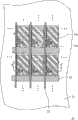
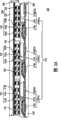
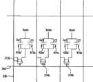
图3A为本发明第一实施例的电子墨水显示面板的结构示意图,图3B为图3A中的电子墨水显示面板的主动元件阵列基板的俯视图,其中图3A的电子墨水显示面板的主动元件阵列基板是沿着图3B中的剖面线C-C’的剖面图。请同时参照图3A与图3B,电子墨水显示面板100包括一主动元件阵列基板200、一前盖板300以及一电子墨水层400。其中,主动元件阵列基板200具有多个像素单元210,且每一像素单元210包括多个次像素单元Px,而每一次像素单元Px还具有一储存电容器Cs。在同一像素单元210中,至少有其中一个次像素单元Px的储存电容器Cs的电容值与其它次像素单元Px的储存电容器Cs的电容值不同。前盖板300配置于主动元件阵列基板200上方。电子墨水层400则配置于主动元件阵列基板200与前盖板300之间。以下将详细说明各构件的细部结构。3A is a schematic structural view of the electronic ink display panel of the first embodiment of the present invention, and FIG. 3B is a top view of the active element array substrate of the electronic ink display panel in FIG. 3A, wherein the active element array substrate of the electronic ink display panel in FIG. 3A is a cross-sectional view along the section line CC' in FIG. 3B. Please refer to FIG. 3A and FIG. 3B at the same time. The electronic
在本实施例中,主动元件阵列基板200包括一基板220、多条扫描线230以及多条数据线240。扫描线230以及数据线240配置于基板220上,且于基板220上定义出多个像素区域220a。In this embodiment, the active
在主动元件阵列基板200中,每一像素单元210还包括一第一第一次像素单元212、一第二次像素单元214以及一第三次像素单元216。每一像素单元210的第一次像素单元212、第二次像素单元214以及第三次像素单元216与同一扫描线230电性相连,且分别位于并排设置的三个像素区域210a中。In the active
更详细而言,第一次像素单元212具有一第一储存电容212a、一第一主动元件212b以及一第一像素电极212c。第二次像素单元214具有一第二储存电容214a、一第二主动元件214b以及一第二像素电极214c。第三次像素单元216具有一第三储存电容器216a、一第三主动元件216b以及一第三像素电极216c。第一主动元件212b、第二主动元件214b以及第三主动元件216b分别与其中一扫描线230以及其中一数据线240电性相连。第一像素电极212c、第二像素电极214c以及第三像素电极216c则分别与对应的第一主动元件212b、第二主动元件214b以及第三主动元件216b电性连接。In more detail, the
前盖板300包括一共享电极310以及一保护膜320。共享电极310配置于电子墨水层400上。保护膜320配置于共享电极310上。The
电子墨水层400包括多个第一墨水材料图案410、多个第二墨水材料图案420以及多个第三墨水材料图案430。其中,第一墨水材料图案配410置于第一像素电极212c上。第二墨水材料图案420配置于第二像素电极214c上。第三墨水材料图430案配置于第三次像素电极216c上。The
承上述,基板220例如为玻璃基板、石英基板或是其它适当材料的基板。扫描线230的材质例如为铝、铝合金或其它适当的导电材料。数据线240的材质例如为铬、铝、合金或是其它适当的导电材料。第一主动元件212b、第二主动元件214b以及第三主动元件216b例如为薄膜晶体管、二极管或是其它具有三端子的开关元件。但需注意的是,在本实施例中,第一主动元件212b、第二主动元件214b以及第三主动元件216b都为为薄膜晶体管。第一像素电极212c、第二像素电极214c以及第三像素电极216c的材质可为铟锡氧化物(indium tin oxide,ITO)、铟锌氧化物(indium zinc oxide,IZO)、金属、上述材料组合的一或是其它适当的材料。共享电极310的材质可为铟锡氧化物、铟锌氧化物或是其它适当的材料。保护膜320的材质例如为塑料、压克力或是其它适当的材质。Based on the above, the
第一墨水材料图案410例如包括多个微胶囊412,其中微胶囊412包含多个第一粒子412a、多个第二粒子412b以及一透明流体412c。第一粒子例如为红色带电染料,第二粒子412b例如为其它颜色的带电染料,且第一粒子412a的电性与第二粒子412b的电性相反。第二墨水材料图案420例如包括多个微胶囊422,其中微胶囊422包含多个第三粒子422a、多个第四粒子422b以及一透明流体422c。第三粒子422a例如为绿色带电染料,第四粒子422b例如为其它颜色的带电染料,且第三粒子422a的电性与第四粒子422b的电性相反。第三墨水材料图案430例如包括多个微胶囊432,其中微胶囊432包含多个第五粒子432a、多个第六粒子432b以及一透明流体432c。第五粒子422a例如为蓝色带电染料,第六粒子432b例如为其它颜色的带电染料,且第五粒子432a的电性与第六粒子432b的电性相反。The first
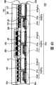
图3C为图3A的电子墨水显示面板的局部等效电路图。请同时参照图3A与图3C,在电子墨水显示面板100中,共享电极310、其中一第一墨水材料图案410以及对应的第一像素电极212c构成一第一显示电容器410a,其电容值为Ce1。共享电极310、其中一第二墨水材料图案420以及对应的第二像素电极214c构成一第二显示电容器420a,其电容值为Ce2。共享电极310、其中一第三墨水材料图案430以及对应的第三像素电极216c构成一第三显示电容器430a,其电容值为Ce3。FIG. 3C is a partial equivalent circuit diagram of the electronic ink display panel of FIG. 3A . Please refer to FIG. 3A and FIG. 3C at the same time. In the electronic
在本实施例中,为了使电子墨水显示面板100能显示彩色画面,故以具有不同颜色的第一墨水材料图案410、第二墨水材料图案420以及第三墨水材料图案430组成电子墨水层400。由于第一墨水材料图案410、第二墨水材料图案420、第三墨水材料图案430的材质不同,因此第一墨水材料410、第二墨水材料420以及第三墨水材料430的介电系数也会不同。如此将造成第一显示电容器410a的电容值Ce1、第二显示电容器420a的电容值Ce2以及第三显示电容器430a的电容值Ce3都不相同,即Ce1≠Ce2≠Ce3。In this embodiment, in order to enable the electronic
此外,第一储存电容器212a的电容值为C1,第二储存电容器214a的电容值为C2,而第三储存电容器216a的电容值为C3。然而,为了使C1+Ce1=C2+Ce2=C3+Ce3,第一储存电容器212a所占据的面积被设计为A1,第二储存电容器214a所占据的面积被设计为A2,且第三储存电容器216a所占据的面积被设计为A3,而A1≠A2≠A3。通过将A1、A2与A3设计为具有不的值,以使C1≠C2≠C3,进而使总电容值相同。类似地,第一墨水材料图案410、第二墨水材料图案420以及第三墨水材料图案430中的微胶囊若仅包含有不同颜色的带电染料和不透明液体的微胶囊,上述的结构也可使电子墨水显示装置100达到总电容值相等的目的。In addition, the capacitance value of the
需注意的是,在本实施例中,第一储存电容器212a、第二储存电容器214a以及第三储存电容器216a虽然分别具有不同的电容值C1、C2以及C3。然而,第一储存电容器212a、第二储存电容器214a以及第三储存电容器216a并不限定必须分别具有不同的电容值。在其它的实施例中,第一储存电容器212a例如具有与第二储存电容器214a不同的电容值,第三储存电容器216a例如具有与第二储存电容器214a相同的电容值,即C1≠C2,C2=C3。It should be noted that, in this embodiment, although the
图3D为根据本发明的第一较佳实施例的又一种电子墨水显示装置110的结构示意图。电子墨水显示装置110系类似于电子墨水显示装置100,但不同之处为:电子墨水显示装置110的电子墨水层400系使用双色带电粒子413、423和433来取代电子墨水显示装置100的微胶囊412、422和432。第一墨水材料图案410包括多个双色带电粒子413,其中双色带电粒子413的一表面布满多个第一粒子412a而双色带电粒子413的另一表面布满多个第二粒子412b。第一粒子例如为红色带电染料,第二粒子412b例如为其它颜色的带电染料,且第一粒子412a的电性与第二粒子412b的电性相反。第二墨水材料图案420例如包括多个双色带电粒子423,其中双色带电粒子423的一表面布满多个第三粒子422a而双色带电粒子423的另一表面布满多个第四粒子422b。第三粒子422a例如为绿色带电染料,第四粒子422b例如为其它颜色的带电染料,且第三粒子422a的电性与第四粒子422b的电性相反。第三墨水材料图案430例如包括多个双色带电粒子433,其中双色带电粒子433的一表面布满多个第五粒子432a而双色带电粒子433的另一表面布满多个第六粒子432b。第五粒子422a例如为蓝色带电染料,第六粒子432b例如为其它颜色的带电染料,且第五粒子432a的电性与第六粒子432b的电性相反。FIG. 3D is a schematic structural diagram of another electronic
图3E为根据本发明的第一较佳实施例的再一种电子墨水显示装置120的结构示意图。电子墨水显示装置120类似于电子墨水显示装置100,但不同之处为:微胶囊412、422和432包含不透明流体和带电粒子。第一墨水材料图案410包含多个微胶囊412,其中微胶囊412包含多个第一粒子47a(例如为红色带电染料)和具有其它颜色的不透明流体46a。第二墨水材料图案420包含多个微胶囊422,其中微胶囊422包含多个第二粒子47b(例如为绿色带电染料)和具有其它颜色的不透明流体46b。第三墨水材料图案430包含多个微胶囊432,其中微胶囊432包含多个第三粒子47c(例如为蓝色带电染料)和具有其它颜色的不透明流体46c。FIG. 3E is a schematic structural diagram of another electronic
第二实施例second embodiment
图4A为本发明第二实施例的电子墨水显示面板的结构示意图,图4B为图4A中的电子墨水显示面板的主动元件阵列基板的俯视图,其中图4A的电子墨水显示面板的主动元件阵列基板是沿着图4B中的剖面线D-D’的剖面图。请同时参照图4A与图4B,电子墨水显示面板500与电子墨水显示装置100类似,其不同之处在于:在电子墨水材料层600中,第一墨水材料图案610的厚度为d1,第二墨水材料图案620的厚度为d2,且第三墨水材料图案630的厚度为d3,而d1≠d2≠d3。需注意的是,第一墨水材料图案610、第二墨水材料图案620以及第三墨水材料图案630包含不同颜色的带电染料。4A is a schematic structural diagram of an electronic ink display panel according to the second embodiment of the present invention, and FIG. 4B is a top view of the active element array substrate of the electronic ink display panel in FIG. 4A, wherein the active element array substrate of the electronic ink display panel in FIG. 4A It is a sectional view along the section line DD' in FIG. 4B. Please refer to FIG. 4A and FIG. 4B at the same time, the electronic
图4C为图4A的电子墨水显示面板的局部等效电路图。请同时参照图4A与图4C,类似于第一实施例,共享电极710、其中一第一墨水材料图案610以及对应的第一像素电极212c构成一第一显示电容器610a,其电容值为Ce1。共享电极710、其中一第二墨水材料图案620以及对应的第二像素电极214c构成一第二显示电容器620a,其电容值为Ce2。共享电极710、其中一第三墨水材料图案630以及对应的第三像素电极216c构成一第三显示电容器630a,其电容值为Ce3。FIG. 4C is a partial equivalent circuit diagram of the electronic ink display panel of FIG. 4A . Please refer to FIG. 4A and FIG. 4C at the same time. Similar to the first embodiment, the shared
本实施例中,调整第一储存电容212a、第二储存电容214a以及第三储存电容器216a所占据的面积A1、A2以及A3,以达到总电容值相等的目的。In this embodiment, the areas A1 , A2 , and A3 occupied by the
此外,还可通过改变第一墨水材料图案610、第二墨水材料图案620以及第三墨水材料图案630的厚度为d1、d2以及d3,以改变第一显示电容器610a的电容值Ce1、第二显示电容器620a的电容值Ce2以及第三显示电容器630a的电容值Ce3,使总电容值相等。类似地,第一墨水材料图案610、第二墨水材料图案620以及第三墨水材料图案630中的微胶囊若仅包含有不同颜色的带电染料和不透明液体的微胶囊,上述的结构也可使电子墨水显示装置500达到总电容值相等的目的。In addition, by changing the thicknesses of the first
由于电子墨水显示面板500具有与第一实施例的电子墨水显示面板100相同的优点,故在此不再赘述。Since the electronic
图4D为根据本发明的第二实施例的又一种电子墨水显示装置510的结构示意图。电子墨水显示装置510类似于电子墨水显示装置500,但不同之处为:电子墨水显示装置510的电子墨水层400使用双色带电粒子413、423和433来取代电子墨水显示装置500的微胶囊412、422和432。FIG. 4D is a schematic structural diagram of another electronic
图4E为根据本发明的第二实施例的再一种电子墨水显示装置710的结构示意图。电子墨水显示装置710类似于电子墨水显示装置500,但不同之处为:电子墨水显示装置710的微胶囊412包含不透明流体46a和第一带电粒子47a;微胶囊422包含不透明流体46b和第二带电粒子47b;微胶囊432包含不透明流体46c和第三带电粒子47c。FIG. 4E is a schematic structural diagram of another electronic
第三实施例third embodiment
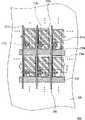
图5A为本发明第三实施例的电子墨水显示面板的结构示意图,图5B为图5A中的电子墨水显示面板的主动元件阵列基板的俯视图,图5C为图3A的电子墨水显示面板的局部等效电路图。其中,图5A的电子墨水显示面板的主动元件阵列基板是沿着图5B中的剖面线E-E’的剖面图。请同时参照图5A至图5C,电子墨水显示面板800与电子墨水显示装置100类似,不同之处在于:共享电极310与主动元件阵列基板900的每一第一像素电极912c重迭的面积为B1,共享电极310与每一第二像素电极914c重迭的面积为B2,共享电极310与每一第三像素电极916c重迭的面积为B3,而B1≠B2≠B3。5A is a schematic structural diagram of an electronic ink display panel according to a third embodiment of the present invention, FIG. 5B is a top view of the active element array substrate of the electronic ink display panel in FIG. 5A , and FIG. 5C is a partial view of the electronic ink display panel in FIG. 3A , etc. Effective circuit diagram. Wherein, the active element array substrate of the electronic ink display panel in FIG. 5A is a cross-sectional view along the section line E-E' in FIG. 5B. Please refer to FIG. 5A to FIG. 5C at the same time. The electronic
本实施例中,通过调整第一储存电容212a、第二储存电容214a以及第三储存电容器216a所占据的面积A1、A2以及A3,以达到总电容值相等的目的。In this embodiment, by adjusting the areas A1 , A2 and A3 occupied by the
除上述方法以外,还可通过改变B1、B2以及B3以改变第一显示电容器410a’的电容值Ce1、第二显示电容器420a’的电容值Ce2以及第三显示电容器430a’的电容值Ce3,使C1+Ce1=C2+Ce2=C3+Ce3。类似地,电子墨水层400中的微胶囊若仅包含有不同颜色的带电染料和不透明液体的微胶囊,上述的结构也可使电子墨水显示装置800达到总电容值相等的目的。In addition to the above method, the capacitance value Ce1 of the
由于电子墨水显示面板800具有与第一实施例的电子墨水显示面板100相同的优点,故在此不再赘述。Since the electronic
图5D为根据本发明的第三实施例的又一种电子墨水显示装置810的结构示意图。电子墨水显示装置810类似于电子墨水显示装置800,但不同之处为:电子墨水显示装置810的电子墨水层400使用双色带电粒子413、423和433来取代电子墨水显示装置800的微胶囊412、422和423。FIG. 5D is a schematic structural diagram of another electronic
图5E为根据本发明的第二实施例的再一种电子墨水显示装置850的结构示意图。电子墨水显示装置850类似于电子墨水显示装置500,但不同之处为:电子墨水显示装置850的微胶囊412包含不透明流体46a和第一粒子47a;微胶囊422包含不透明流体46b和第二带电粒子47b;微胶囊432包含不透明流体46c和第三带电粒子47c。FIG. 5E is a schematic structural diagram of another electronic ink display device 850 according to the second embodiment of the present invention. The electronic ink display device 850 is similar to the electronic
综上所述,在本发明提出的电子墨水显示面板中,储存电容的电容值与共享电极、其中一墨水材料图案以及对应的像素电极构成的显示电容器的电容值相互补偿,以使储存电容与对应的显示电容器的总电容值都为相等。其方法包括调整储存电容占据的面积、墨水材料图案的厚度以及共享电极与对应的像素电极重迭的面积。To sum up, in the electronic ink display panel proposed by the present invention, the capacitance value of the storage capacitor and the capacitance value of the display capacitor composed of the shared electrode, one of the ink material patterns and the corresponding pixel electrode are mutually compensated, so that the storage capacitor and The total capacitance values of the corresponding display capacitors are all equal. The method includes adjusting the area occupied by the storage capacitor, the thickness of the ink material pattern, and the overlapping area of the shared electrode and the corresponding pixel electrode.
当然,本发明还可有其它多种实施例,在不背离本发明精神及其实质的情况下,熟悉本领域的普通技术人员当可根据本发明做出各种相应的改变和变形,但这些相应的改变和变形都应属于本发明所附的权利要求的保护范围。Certainly, the present invention also can have other various embodiments, without departing from the spirit and essence of the present invention, those skilled in the art can make various corresponding changes and deformations according to the present invention, but these Corresponding changes and deformations should belong to the scope of protection of the appended claims of the present invention.
Claims (18)
Priority Applications (1)
| Application Number | Priority Date | Filing Date | Title |
|---|---|---|---|
| CN2007101070285ACN101308309B (en) | 2007-05-17 | 2007-05-17 | Electronic ink display panel |
Applications Claiming Priority (1)
| Application Number | Priority Date | Filing Date | Title |
|---|---|---|---|
| CN2007101070285ACN101308309B (en) | 2007-05-17 | 2007-05-17 | Electronic ink display panel |
Publications (2)
| Publication Number | Publication Date |
|---|---|
| CN101308309A CN101308309A (en) | 2008-11-19 |
| CN101308309Btrue CN101308309B (en) | 2010-11-17 |
Family
ID=40124813
Family Applications (1)
| Application Number | Title | Priority Date | Filing Date |
|---|---|---|---|
| CN2007101070285AActiveCN101308309B (en) | 2007-05-17 | 2007-05-17 | Electronic ink display panel |
Country Status (1)
| Country | Link |
|---|---|
| CN (1) | CN101308309B (en) |
Families Citing this family (1)
| Publication number | Priority date | Publication date | Assignee | Title |
|---|---|---|---|---|
| TWI880349B (en)* | 2023-09-14 | 2025-04-11 | 速博思股份有限公司 | Electrophoresis display with transparent control electrode |
Citations (5)
| Publication number | Priority date | Publication date | Assignee | Title |
|---|---|---|---|---|
| US6762744B2 (en)* | 2000-06-22 | 2004-07-13 | Seiko Epson Corporation | Method and circuit for driving electrophoretic display, electrophoretic display and electronic device using same |
| US6774884B2 (en)* | 2000-12-01 | 2004-08-10 | Seiko Epson Corporation | Electrophoretic device, electronic sheet including the same, electronic book including the electronic sheet, and manufacturing method thereof |
| CN1527118A (en)* | 2003-03-03 | 2004-09-08 | Electronic ink display device | |
| CN1834763A (en)* | 2005-03-18 | 2006-09-20 | 精工爱普生株式会社 | Electrophoretic display device and driving method thereof |
| CN101004528A (en)* | 2006-01-18 | 2007-07-25 | 三星电子株式会社 | Electrophoretic indication display |
- 2007
- 2007-05-17CNCN2007101070285Apatent/CN101308309B/enactiveActive
Patent Citations (5)
| Publication number | Priority date | Publication date | Assignee | Title |
|---|---|---|---|---|
| US6762744B2 (en)* | 2000-06-22 | 2004-07-13 | Seiko Epson Corporation | Method and circuit for driving electrophoretic display, electrophoretic display and electronic device using same |
| US6774884B2 (en)* | 2000-12-01 | 2004-08-10 | Seiko Epson Corporation | Electrophoretic device, electronic sheet including the same, electronic book including the electronic sheet, and manufacturing method thereof |
| CN1527118A (en)* | 2003-03-03 | 2004-09-08 | Electronic ink display device | |
| CN1834763A (en)* | 2005-03-18 | 2006-09-20 | 精工爱普生株式会社 | Electrophoretic display device and driving method thereof |
| CN101004528A (en)* | 2006-01-18 | 2007-07-25 | 三星电子株式会社 | Electrophoretic indication display |
Also Published As
| Publication number | Publication date |
|---|---|
| CN101308309A (en) | 2008-11-19 |
Similar Documents
| Publication | Publication Date | Title |
|---|---|---|
| JP4851397B2 (en) | Electronic ink display panel | |
| KR102113607B1 (en) | Liquid crystal display device and method of fabricating the same | |
| KR101108782B1 (en) | Liquid Crystal Display device and the fabrication method thereof | |
| KR100951351B1 (en) | Thin film transistor array panel and electrophoretic display device including the same | |
| CN104603685A (en) | Liquid crystal display device | |
| JP7266741B2 (en) | Display device | |
| KR101247680B1 (en) | Electrophoretic Display Device and Method for Manufacturing thereof | |
| KR20130024097A (en) | Flexible display device and method for manufacturing the same | |
| TWI454815B (en) | Electrophoretic display device and method for manufacturing the same | |
| CN109839779A (en) | Liquid crystal display panel | |
| US7903320B2 (en) | Electrophoretic display device and electronic apparatus | |
| CN101930147A (en) | Electrophoretic display device | |
| CN105093600A (en) | Display panel and display device | |
| CN103217821A (en) | Display device and manufacturing method thereof | |
| US7548366B2 (en) | Electrophoretic display module and electrophoretic display device | |
| KR20060030630A (en) | Electrophoretic display device and manufacturing method thereof | |
| CN101308309B (en) | Electronic ink display panel | |
| TW201403198A (en) | Electrophoretic display | |
| US20130313557A1 (en) | Display apparatus | |
| KR20130024391A (en) | Flexible display device | |
| KR20120051338A (en) | Electrophoretic display device | |
| CN118276368A (en) | Electronic paper display device and manufacturing method thereof | |
| KR20120063124A (en) | Mother substrate device of electrophoretic display and method for manufacturing electrophoretic display using the same | |
| KR20120007664A (en) | Electrophoresis display |
Legal Events
| Date | Code | Title | Description |
|---|---|---|---|
| C06 | Publication | ||
| PB01 | Publication | ||
| C10 | Entry into substantive examination | ||
| SE01 | Entry into force of request for substantive examination | ||
| C14 | Grant of patent or utility model | ||
| GR01 | Patent grant |