CN101308271B - Liquid crystal panel, LCD display device and its drive method - Google Patents
Liquid crystal panel, LCD display device and its drive methodDownload PDFInfo
- Publication number
- CN101308271B CN101308271BCN2008101260392ACN200810126039ACN101308271BCN 101308271 BCN101308271 BCN 101308271BCN 2008101260392 ACN2008101260392 ACN 2008101260392ACN 200810126039 ACN200810126039 ACN 200810126039ACN 101308271 BCN101308271 BCN 101308271B
- Authority
- CN
- China
- Prior art keywords
- pixel
- common
- voltage
- liquid crystal
- voltage signal
- Prior art date
- Legal status (The legal status is an assumption and is not a legal conclusion. Google has not performed a legal analysis and makes no representation as to the accuracy of the status listed.)
- Expired - Fee Related
Links
Images


Classifications
- G—PHYSICS
- G09—EDUCATION; CRYPTOGRAPHY; DISPLAY; ADVERTISING; SEALS
- G09G—ARRANGEMENTS OR CIRCUITS FOR CONTROL OF INDICATING DEVICES USING STATIC MEANS TO PRESENT VARIABLE INFORMATION
- G09G3/00—Control arrangements or circuits, of interest only in connection with visual indicators other than cathode-ray tubes
- G09G3/20—Control arrangements or circuits, of interest only in connection with visual indicators other than cathode-ray tubes for presentation of an assembly of a number of characters, e.g. a page, by composing the assembly by combination of individual elements arranged in a matrix no fixed position being assigned to or needed to be assigned to the individual characters or partial characters
- G09G3/34—Control arrangements or circuits, of interest only in connection with visual indicators other than cathode-ray tubes for presentation of an assembly of a number of characters, e.g. a page, by composing the assembly by combination of individual elements arranged in a matrix no fixed position being assigned to or needed to be assigned to the individual characters or partial characters by control of light from an independent source
- G09G3/36—Control arrangements or circuits, of interest only in connection with visual indicators other than cathode-ray tubes for presentation of an assembly of a number of characters, e.g. a page, by composing the assembly by combination of individual elements arranged in a matrix no fixed position being assigned to or needed to be assigned to the individual characters or partial characters by control of light from an independent source using liquid crystals
- G09G3/3611—Control of matrices with row and column drivers
- G09G3/3648—Control of matrices with row and column drivers using an active matrix
- G—PHYSICS
- G09—EDUCATION; CRYPTOGRAPHY; DISPLAY; ADVERTISING; SEALS
- G09G—ARRANGEMENTS OR CIRCUITS FOR CONTROL OF INDICATING DEVICES USING STATIC MEANS TO PRESENT VARIABLE INFORMATION
- G09G2300/00—Aspects of the constitution of display devices
- G09G2300/04—Structural and physical details of display devices
- G09G2300/0421—Structural details of the set of electrodes
- G09G2300/0426—Layout of electrodes and connections
- G—PHYSICS
- G09—EDUCATION; CRYPTOGRAPHY; DISPLAY; ADVERTISING; SEALS
- G09G—ARRANGEMENTS OR CIRCUITS FOR CONTROL OF INDICATING DEVICES USING STATIC MEANS TO PRESENT VARIABLE INFORMATION
- G09G2300/00—Aspects of the constitution of display devices
- G09G2300/08—Active matrix structure, i.e. with use of active elements, inclusive of non-linear two terminal elements, in the pixels together with light emitting or modulating elements
- G09G2300/0876—Supplementary capacities in pixels having special driving circuits and electrodes instead of being connected to common electrode or ground; Use of additional capacitively coupled compensation electrodes
- G—PHYSICS
- G09—EDUCATION; CRYPTOGRAPHY; DISPLAY; ADVERTISING; SEALS
- G09G—ARRANGEMENTS OR CIRCUITS FOR CONTROL OF INDICATING DEVICES USING STATIC MEANS TO PRESENT VARIABLE INFORMATION
- G09G3/00—Control arrangements or circuits, of interest only in connection with visual indicators other than cathode-ray tubes
- G09G3/20—Control arrangements or circuits, of interest only in connection with visual indicators other than cathode-ray tubes for presentation of an assembly of a number of characters, e.g. a page, by composing the assembly by combination of individual elements arranged in a matrix no fixed position being assigned to or needed to be assigned to the individual characters or partial characters
- G09G3/34—Control arrangements or circuits, of interest only in connection with visual indicators other than cathode-ray tubes for presentation of an assembly of a number of characters, e.g. a page, by composing the assembly by combination of individual elements arranged in a matrix no fixed position being assigned to or needed to be assigned to the individual characters or partial characters by control of light from an independent source
- G09G3/36—Control arrangements or circuits, of interest only in connection with visual indicators other than cathode-ray tubes for presentation of an assembly of a number of characters, e.g. a page, by composing the assembly by combination of individual elements arranged in a matrix no fixed position being assigned to or needed to be assigned to the individual characters or partial characters by control of light from an independent source using liquid crystals
- G09G3/3611—Control of matrices with row and column drivers
- G09G3/3614—Control of polarity reversal in general
Landscapes
- Engineering & Computer Science (AREA)
- Chemical & Material Sciences (AREA)
- Crystallography & Structural Chemistry (AREA)
- Physics & Mathematics (AREA)
- Computer Hardware Design (AREA)
- General Physics & Mathematics (AREA)
- Theoretical Computer Science (AREA)
- Liquid Crystal (AREA)
- Liquid Crystal Display Device Control (AREA)
- Control Of Indicators Other Than Cathode Ray Tubes (AREA)
Abstract
Translated fromChinese
Description
Translated fromChinese技术领域technical field
本发明涉及一种液晶面板、液晶显示装置及其驱动方法。The invention relates to a liquid crystal panel, a liquid crystal display device and a driving method thereof.
背景技术Background technique
液晶显示装置(Liquid Crystal Display,LCD)以低功耗、轻、薄等特点而被广泛应用于个人计算机屏幕、液晶电视、手机或个人数字助理(PDA)等现代化电子设备中。Liquid Crystal Display (LCD) is widely used in modern electronic devices such as personal computer screens, LCD TVs, mobile phones or personal digital assistants (PDAs) due to its low power consumption, lightness, and thinness.
通常,液晶显示装置采用电场来控制液晶的通光率,以显示图像。根据液晶的电场驱动方向,可以将液晶大致分类为水平电场型和垂直电场型。水平电场施加型液晶显示装置采用在下基板上彼此平行设置的像素电极和公共电极之间形成的水平电场、以面内切换(IPS,In-PlaneSwitching)模式来驱动液晶。垂直电场施加型液晶显示装置采用在上基板和下基板上彼此相对设置的像素电极和公共电极之间的垂直电场以扭曲向列(TN,Twisted Nematic)模式来驱动液晶。Generally, a liquid crystal display device uses an electric field to control the transmittance of liquid crystals to display images. Liquid crystals can be roughly classified into a horizontal electric field type and a vertical electric field type according to the electric field driving direction of the liquid crystal. The horizontal electric field application type liquid crystal display device uses the horizontal electric field formed between the pixel electrode and the common electrode arranged in parallel to each other on the lower substrate to drive the liquid crystal in an In-Plane Switching (IPS, In-Plane Switching) mode. The vertical electric field application type liquid crystal display device uses a vertical electric field between the pixel electrode and the common electrode disposed opposite to each other on the upper substrate and the lower substrate to drive the liquid crystal in a twisted nematic (TN, Twisted Nematic) mode.
在液晶显示装置中,存在单纯矩阵型和对像素利用了TFT(Thin FilmTransistor,薄膜晶体管)等有源元件的有源矩阵型等。有源矩阵型液晶显示装置的驱动方法包括帧反转驱动、H行反转(行反转)驱动、V行反转(列反转)驱动、点反转驱动等驱动方法。以下参照附图来举例说明现有技术中采用不同驱动方法的有源矩阵型液晶显示装置。Liquid crystal display devices include a simple matrix type and an active matrix type using active elements such as TFTs (Thin Film Transistors, thin film transistors) for pixels. The driving method of the active matrix type liquid crystal display device includes driving methods such as frame inversion driving, H row inversion (row inversion) driving, V row inversion (column inversion) driving, and dot inversion driving. The active matrix liquid crystal display devices using different driving methods in the prior art will be illustrated below with reference to the accompanying drawings.
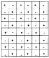
参照图1及图2来示意性地说明采用列反转驱动的液晶显示装置。图1是在液晶显示装置采用列反转驱动时,其液晶面板的像素单元极性的示意图。如图1所示,在当前帧中,奇数列像素单元的极性为正,偶数列像素单元的极性为负。图2是图1所示的液晶面板中部分像素单元的电路示意图。为了简单起见,图2中仅示出了部分电路结构。如图2所示,同一行像素单元中的TFT 20的栅极20g连接到同一扫描线上,同一列像素单 元具有相同的极性,且同一列像素单元中的TFT 20的源极20s连接到同一数据线上,每个像素单元中TFT 20的漏极20d连接到相应的像素电极22。例如,图2中的第一行像素单元中的TFT 20的栅极20g连接到扫描线G1上,第一列像素单元在当前帧中具有正极性且第一列像素单元中的TFT 20的源极20s连接到数据线D1上。A liquid crystal display device employing column inversion driving is schematically described with reference to FIGS. 1 and 2 . FIG. 1 is a schematic diagram of the polarity of pixel units of a liquid crystal panel when the liquid crystal display device adopts column inversion driving. As shown in FIG. 1 , in the current frame, the polarity of pixel units in odd columns is positive, and the polarity of pixel units in even columns is negative. FIG. 2 is a schematic circuit diagram of some pixel units in the liquid crystal panel shown in FIG. 1 . For simplicity, only part of the circuit structure is shown in FIG. 2 . As shown in Figure 2, the
参照图3及图4来示意性地说明采用点反转驱动的液晶显示装置。图3是在液晶显示装置采用点反转驱动时,其液晶面板的像素单元极性的示意图。如图3所示,与列反转驱动和其他驱动方法不同,每个像素单元都与其上下左右所紧邻的像素单元的极性不同。图4是图3所示的液晶面板中部分像素单元的电路示意图。同样为了简单起见,图4中仅示出了部分电路结构。如图4所示,奇数列的相邻两行像素单元中的TFT 40的栅极40g连接到同一扫描线上,偶数列的相邻两行像素单元中的TFT 40的栅极40g连接到另一扫描线上,同一列中具有相同极性的像素单元中的TFT 40的源极40s连接到同一数据线上,每个像素单元中TFT 40的漏极40d连接到相应的像素电极42。例如,在图4中,像素单元P11、P13、P21和P23中的TFT 40的栅极连接到扫描线G1上,像素单元P22、P24、P32和P34中的TFT 40的栅极40g连接到扫描线G2上,像素单元P11和P31中的TFT 40的源极40s连接到数据线D1上。A liquid crystal display device using dot inversion driving will be schematically described with reference to FIGS. 3 and 4 . 3 is a schematic diagram of the polarity of the pixel units of the liquid crystal panel when the liquid crystal display device adopts dot inversion driving. As shown in FIG. 3 , different from column inversion driving and other driving methods, each pixel unit has a different polarity from its upper, lower, left, and right adjacent pixel units. FIG. 4 is a schematic circuit diagram of some pixel units in the liquid crystal panel shown in FIG. 3 . Also for the sake of simplicity, only part of the circuit structure is shown in FIG. 4 . As shown in Figure 4, the
一种现有的有源矩阵型液晶面板,通常包括n行互相平行的扫描线,m列互相平行且与这n行扫描线垂直绝缘相交的数据线,以及多个像素单元。每个像素单元包括薄膜晶体管、液晶电容CLC及存储电容Cst。薄膜晶体管位于扫描线和数据线的相交处,其作为开关元件来驱动像素电极。薄膜晶体管的栅极连接到扫描线以接收扫描线所传输的扫描信号,源极连接到数据线,漏极连接到像素电极。扫描线和数据线所围的最小区域定义为像素区域。每一行像素包括m个像素电极,像素电极与对置基板的公共电极(也称对置电极)之间形成液晶电容CLC。像素电极与阵列基板的公共电极(也称存储电极)之间形成存储电容Cst。An existing active matrix liquid crystal panel usually includes n rows of scanning lines parallel to each other, m columns of data lines parallel to each other and vertically insulated and intersecting with the n rows of scanning lines, and a plurality of pixel units. Each pixel unit includes a thin film transistor, a liquid crystal capacitor CLC and a storage capacitor Cst . Thin film transistors are located at intersections of scan lines and data lines, and serve as switching elements to drive pixel electrodes. The gate of the thin film transistor is connected to the scan line to receive the scan signal transmitted by the scan line, the source is connected to the data line, and the drain is connected to the pixel electrode. The smallest area surrounded by scan lines and data lines is defined as a pixel area. Each row of pixels includes m pixel electrodes, and a liquid crystal capacitance CLC is formed between the pixel electrodes and the common electrode (also called the opposite electrode) of the opposite substrate. A storage capacitor Cst is formed between the pixel electrode and a common electrode (also referred to as a storage electrode) of the array substrate.
液晶电容的第一端(即像素电极)通过薄膜晶体管的漏极和源极而与数据线耦接,液晶电容的第二端则连接至对置基板以接收公共电压信号 Vcom。存储电容的第一端与液晶电容的第一端连接,存储电容的第二端则连接至阵列基板上以接收公共电压信号Vcom。当对液晶面板进行扫描时,在一帧时间内产生多个扫描信号,这些扫描信号被施加至各条扫描线。当扫描信号使薄膜晶体管导通时,数据信号电压藉数据线通过薄膜晶体管的源极和漏极传输至液晶电容的第一端与存储电容的第一端,从而对液晶电容和存储电容进行充电。The first end of the liquid crystal capacitor (that is, the pixel electrode) is coupled to the data line through the drain and source of the thin film transistor, and the second end of the liquid crystal capacitor is connected to the opposite substrate to receive the common voltage signal Vcom. The first end of the storage capacitor is connected to the first end of the liquid crystal capacitor, and the second end of the storage capacitor is connected to the array substrate to receive the common voltage signal Vcom. When scanning the liquid crystal panel, a plurality of scanning signals are generated within one frame time, and these scanning signals are applied to the respective scanning lines. When the scanning signal turns on the thin film transistor, the data signal voltage is transmitted to the first end of the liquid crystal capacitor and the first end of the storage capacitor through the source and drain of the thin film transistor through the data line, thereby charging the liquid crystal capacitor and the storage capacitor .
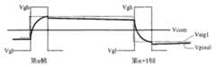
以下参照图5A和图5B来说明现有技术的液晶面板(例如图1至图4所示的液晶面板)中的像素单元在被驱动时,其像素电压、数据信号电压、公共电压信号和扫描信号的波形。在图5A和图5B中,Vgh代表扫描线的高电压(也称为扫描开启信号),Vgl代表扫描线的低电压,Vsig1、Vsig2代表提供给数据线上的数据信号电压,Vpixel代表像素电极充电的电压(也称为像素电压),Vcom代表提供给像素单元的公共电极的公共电压信号。The pixel voltage, data signal voltage, common voltage signal and scan voltage of the pixel unit in the liquid crystal panel of the prior art (such as the liquid crystal panel shown in FIG. 1 to FIG. 4 ) are described below when being driven The waveform of the signal. In Fig. 5A and Fig. 5B, Vgh represents the high voltage of the scan line (also called the scan-on signal), Vgl represents the low voltage of the scan line, Vsig1 and Vsig2 represent the data signal voltage supplied to the data line, and Vpixel represents the pixel electrode The charging voltage (also referred to as pixel voltage), Vcom represents the common voltage signal provided to the common electrode of the pixel unit.
图5A为图2和图4中的奇数据线上连接的某像素单元的像素电压、数据信号电压、公共电压信号和扫描信号的波形图。为了简单起见,图5A中仅示出关于第n帧和第n+1帧的波形。如图5A所示,对于第n帧,在向某条扫描线施加扫描开启信号期间,高电压Vgh使连接于该扫描线上的薄膜晶体管处于导通状态,即,薄膜晶体管的漏极与源极导通。在此期间,代表第n帧像素电压的数据信号电压Vsig1藉数据线通过薄膜晶体管的源极和漏极施加至像素电极,使连接于该扫描线上的像素单元显示像素电压Vpixel,并使这些像素单元中的存储电容处于充电状态,且由存储电容在该帧的随后时间内保持该像素电压Vpixel。理论上,在第n+1帧的扫描开启信号施加至该扫描线之前,连接于该扫描线上的像素单元显示的像素电压Vpixel保持不变。但实际上,当扫描信号从高电压Vgh转变为低电压Vgl瞬间,薄膜晶体管截止,液晶电容藉由存储电容而维持的充电电压会由于电容耦合效应而突然有所下降,并且在扫描信号保持为低电压Vgl之后会由于邻近的寄生电阻的影响而有少许减小。FIG. 5A is a waveform diagram of pixel voltage, data signal voltage, common voltage signal and scanning signal of a certain pixel unit connected to the odd data line in FIG. 2 and FIG. 4 . For simplicity, only the waveforms about the nth frame and the n+1th frame are shown in FIG. 5A . As shown in FIG. 5A, for the nth frame, during the period when a scan-on signal is applied to a certain scan line, the high voltage Vgh makes the thin-film transistor connected to the scan line be in the conduction state, that is, the drain and source of the thin-film transistor Pole conduction. During this period, the data signal voltage Vsig1 representing the pixel voltage of the nth frame is applied to the pixel electrode through the data line through the source and drain of the thin film transistor, so that the pixel units connected to the scanning line display the pixel voltage Vpixel, and these The storage capacitor in the pixel unit is in a charging state, and the pixel voltage Vpixel is maintained by the storage capacitor in the subsequent time of the frame. Theoretically, before the scan-on signal of frame (n+1) is applied to the scan line, the pixel voltage Vpixel displayed by the pixel units connected to the scan line remains unchanged. But in fact, when the scanning signal changes from high voltage Vgh to low voltage Vgl, the thin film transistor is turned off, and the charging voltage maintained by the liquid crystal capacitor through the storage capacitor will suddenly drop due to the capacitive coupling effect, and when the scanning signal remains at The low voltage Vgl will then be slightly reduced due to the influence of adjacent parasitic resistances.
在第n+1帧的扫描开启信号施加至该扫描线时,该扫描线上连接的像素单元的极性发生反转。与第n帧类似,在第n+1帧的扫描开启信号施加 至该扫描线期间,高电压Vgh使连接于该扫描线上的薄膜晶体管处于导通状态,同时,代表第n+1帧像素电压的数据信号电压Vsig1藉数据线通过薄膜晶体管的源极和漏极施加至像素电极,使连接于该扫描线上的像素单元的显示更新为第n+1帧像素电压Vpixel,并使这些像素单元中的存储电容处于充电状态,且由存储电容在该帧的随后时间内保持该像素电压Vpixel。如此,周而复始。When the scan-on signal of the (n+1)th frame is applied to the scan line, the polarity of the pixel units connected to the scan line is reversed. Similar to the n-th frame, when the scan-on signal of the n+1-th frame is applied to the scan line, the high voltage Vgh makes the thin-film transistor connected to the scan line in the conduction state, and at the same time, represents the pixel of the n+1-th frame The data signal voltage Vsig1 of the voltage is applied to the pixel electrode through the source and drain of the thin film transistor through the data line, so that the display of the pixel unit connected to the scanning line is updated to the n+1th frame pixel voltage Vpixel, and these pixels The storage capacitor in the cell is in a charging state, and the pixel voltage Vpixel is maintained by the storage capacitor in the subsequent time of the frame. So, again and again.
图5B为图2和图4中的偶数据线上连接的某像素单元的像素电压、数据信号电压、公共电压信号和扫描信号的波形图。为了简单起见,图5B中也仅示出关于第n帧和第n+1帧的波形。因为偶数据线上连接的像素单元与奇数据线上连接的像素单元的像素电极的极性相反,即,偶数据线上连接的像素单元的像素电压与奇数据线上连接的像素单元的像素电压在同一帧内极性相反,所以偶数据线上连接的像素单元的像素电压的波形图与奇数据线上连接的像素单元的像素电压的波形图相反。由于在此情况下通过图5A的描述可以清楚地理解图5B,因此这里不再赘述。FIG. 5B is a waveform diagram of pixel voltage, data signal voltage, common voltage signal and scanning signal of a certain pixel unit connected to the even data line in FIG. 2 and FIG. 4 . For the sake of simplicity, FIG. 5B also only shows the waveforms about the nth frame and the n+1th frame. Because the polarity of the pixel unit connected to the even data line is opposite to that of the pixel electrode connected to the odd data line, that is, the pixel voltage of the pixel unit connected to the even data line is the same as that of the pixel voltage of the pixel unit connected to the odd data line. The voltages have opposite polarities in the same frame, so the waveform diagram of the pixel voltage of the pixel unit connected to the even data line is opposite to the waveform diagram of the pixel voltage of the pixel unit connected to the odd data line. Since FIG. 5B can be clearly understood through the description of FIG. 5A in this case, details are not repeated here.
在现有技术的液晶面板显示像素电压时,如果连续两帧画面的图像有所不同,则很容易产生拖影。这是因为液晶材料的反应速度慢、反应时间长。而且,当画面中的物体快速移动时,在扫描一个画面的过程中,液晶材料无法实时追踪物体的轨迹。在这种情况下,液晶材料所产生的是数次画面扫描时间的累积反应。针对液晶材料的特殊属性,为解决其影像残留问题,已提出相当多的研究报告,其中主要有以下三种解决方向:(1)内在性质(intrinsic property):将液晶的粘稠度改变为低黏性(lowviscosity);(2)加大扭转电压,即过压驱动(over driving):使液晶更快地扭转与恢复;(3)插入全黑画面(简称插黑,black insertion):在每一个影像画面显示完之后,在下一个影像画面显示之前,插入一个全黑画面。When a liquid crystal panel in the prior art displays pixel voltages, if the images of two consecutive frames are different, smearing is likely to occur. This is because the reaction speed of the liquid crystal material is slow and the reaction time is long. Moreover, when the object in the picture moves quickly, the liquid crystal material cannot track the trajectory of the object in real time during the process of scanning a picture. In this case, what the liquid crystal material produces is the cumulative response of several screen scan times. Aiming at the special properties of liquid crystal materials, in order to solve the problem of image retention, quite a few research reports have been put forward, among which there are mainly three solutions directions: (1) Intrinsic property: change the viscosity of liquid crystal to low Viscosity (lowviscosity); (2) Increase the reverse voltage, that is, over driving (over driving): make the liquid crystal reverse and recover faster; (3) Insert a full black screen (referred to as black insertion): in each After one image frame is displayed, before the next image frame is displayed, a completely black frame is inserted.
然而,采用改变液晶的粘稠度的方式来提高动态显示画面的质量,会使液晶的其他参数特性也随之改变,这会带来其他一些不利后果。采用过压驱动方式,需要提高驱动电压或者采用电压补偿方式,对驱动电路的要求较高。采用现有的插黑技术,源极驱动电路必须交替产生影像数据与全 黑数据,亦即,不管是影像数据或是插黑数据,这些数据均由源极驱动电路来产生。由于源极驱动电路必须在不同时间产生插黑电压与数据驱动电压,因此,栅极驱动电路的扫描频率也必须加倍,使得源极驱动器的负载大为增加,且源极驱动器的反应速度也必须相应提高。However, improving the quality of dynamic display images by changing the viscosity of the liquid crystal will change other parameters of the liquid crystal, which will bring some other adverse consequences. Using the overvoltage driving method requires increasing the driving voltage or adopting a voltage compensation method, which has higher requirements on the driving circuit. With the existing black insertion technology, the source driver circuit must alternately generate image data and full black data, that is, whether it is image data or black insertion data, these data are all generated by the source driver circuit. Since the source drive circuit must generate the black insertion voltage and the data drive voltage at different times, the scanning frequency of the gate drive circuit must also be doubled, which greatly increases the load on the source driver, and the response speed of the source driver must also be Increase accordingly.
发明内容Contents of the invention
考虑到上述问题,本发明的优选实施例提供了一种液晶面板、液晶显示装置及其驱动方法,可以在不需要提高驱动频率的情况下进行插黑或者插灰处理并且可以具备预充电功能。Considering the above problems, the preferred embodiment of the present invention provides a liquid crystal panel, a liquid crystal display device and its driving method, which can perform black or gray insertion processing without increasing the driving frequency and can have a pre-charging function.
根据本发明的一个技术方案,提供了一种可实现1/2屏插黑的液晶显示装置,其包括液晶面板,液晶面板包括扫描线、数据线和多个像素单元,所述多个像素单元中的每个像素单元包括薄膜晶体管、像素电极、第一公共电极和第二公共电极,其中,所述多个像素单元包括位于上半屏的第一组像素单元和位于下半屏的第二组像素单元,所述第一组像素单元中的第一像素单元的第一公共电极电性连接以接收第一公共电压信号,所述第一组像素单元中的第二像素单元的第一公共电极电性连接以接收第二公共电压信号,所述第二组像素单元中的第一像素单元的第一公共电极电性连接以接收第四公共电压信号,第二组像素单元中的第二像素单元的第一公共电极电性连接以接收第五公共电压信号,所述多个像素单元的第二公共电极电性连接以接收第三公共电压信号,并且,所述第一公共电压信号和所述第二公共电压信号为交流电压信号且在同一帧内极性相反,所述地四公共电压信号和所述第五公共电压信号为交流电压信号且在同一帧内极性相反。According to a technical solution of the present invention, a liquid crystal display device capable of realizing 1/2 screen insertion black is provided, which includes a liquid crystal panel, and the liquid crystal panel includes scanning lines, data lines and a plurality of pixel units, and the plurality of pixel units Each pixel unit in includes a thin film transistor, a pixel electrode, a first common electrode, and a second common electrode, wherein the plurality of pixel units include a first group of pixel units located in the upper half of the screen and a second group of pixel units located in the lower half of the screen. A group of pixel units, the first common electrode of the first pixel unit in the first group of pixel units is electrically connected to receive a first common voltage signal, the first common electrode of the second pixel unit in the first group of pixel units The electrodes are electrically connected to receive a second common voltage signal, the first common electrode of the first pixel unit in the second group of pixel units is electrically connected to receive a fourth common voltage signal, and the second common electrode in the second group of pixel units The first common electrodes of the pixel units are electrically connected to receive a fifth common voltage signal, the second common electrodes of the plurality of pixel units are electrically connected to receive a third common voltage signal, and the first common voltage signal and The second common voltage signal is an AC voltage signal with opposite polarities within the same frame, and the four ground common voltage signals and the fifth common voltage signal are AC voltage signals with opposite polarities within the same frame.
根据本发明的另一个技术方案,提供了一种液晶显示装置的驱动方法,所述液晶显示装置包括具有扫描线、数据线和多个像素单元的液晶面板,所述多个像素单元包括第一像素单元和第二像素单元,每个像素单元包括薄膜晶体管、像素电极、第一公共电极和第二公共电极,所述多个像素单元的第二公共电极电性连接,其中,所述多个像素单元中的第一像素单元的第一公共电极电性连接,所述多个像素单元中的第二像素单元的第一公共电极电性连接,所述驱动方法包括:施加数据信号至所述数据线;在薄膜晶体管开启之前,输入与输入至第一像素单元的数据信号相同极性的第一公共电压信号至第一像素单元的第一公共电极,输入与第二像素单元的数据信号相同极性并且与第一公共电压信号相反极性的第二公共电压信号至第二像素单元的第一公共电极;输入第三公共电压信号至第一像素单元和第二像素单元的第二公共电极。According to another technical solution of the present invention, a driving method of a liquid crystal display device is provided, the liquid crystal display device includes a liquid crystal panel having scanning lines, data lines and a plurality of pixel units, the plurality of pixel units including a first A pixel unit and a second pixel unit, each pixel unit includes a thin film transistor, a pixel electrode, a first common electrode and a second common electrode, the second common electrodes of the plurality of pixel units are electrically connected, wherein the plurality of The first common electrode of the first pixel unit among the pixel units is electrically connected, the first common electrode of the second pixel unit among the plurality of pixel units is electrically connected, and the driving method includes: applying a data signal to the Data line: before the thin film transistor is turned on, input the first common voltage signal with the same polarity as the data signal input to the first pixel unit to the first common electrode of the first pixel unit, and input the same data signal as the second pixel unit A second common voltage signal with a polarity opposite to the first common voltage signal is sent to the first common electrode of the second pixel unit; a third common voltage signal is input to the second common electrodes of the first pixel unit and the second pixel unit .
相较于现有技术,本发明通过提供极性相反的第一和第二公共电压信号,实现了在不需要提高驱动频率的情况下进行插黑或者插灰的技术并且具备预充电的功能。Compared with the prior art, the present invention provides the first and second common voltage signals with opposite polarities to realize the technology of inserting black or gray without increasing the driving frequency and has the function of pre-charging.
附图说明Description of drawings
图1是根据现有技术的液晶显示装置在采用列反转驱动时,其液晶面板的像素单元极性的示意图。FIG. 1 is a schematic diagram of the polarity of pixel units of a liquid crystal panel when a liquid crystal display device in the prior art adopts column inversion driving.
图2是图1所示的液晶面板中部分像素单元的电路示意图。FIG. 2 is a schematic circuit diagram of some pixel units in the liquid crystal panel shown in FIG. 1 .
图3是根据现有技术的液晶显示装置在采用点反转驱动时,其液晶面 板的像素单元极性的示意图。Fig. 3 is a schematic diagram of the polarity of the pixel unit of the liquid crystal panel when the liquid crystal display device according to the prior art adopts dot inversion driving.
图4是图3所示的液晶面板中部分像素单元的电路示意图。FIG. 4 is a schematic circuit diagram of some pixel units in the liquid crystal panel shown in FIG. 3 .
图5A和图5B分别是图2和图4中的奇数据线和偶数据线上连接的某像素单元的像素电压、数据信号电压、公共电压信号和扫描信号的波形图。5A and 5B are waveform diagrams of pixel voltage, data signal voltage, common voltage signal and scanning signal of a certain pixel unit connected to the odd data line and even data line in FIG. 2 and FIG. 4 respectively.
图6是根据本发明第一实施例的液晶显示装置在采用点反转驱动时,其液晶面板的阵列基板侧部分像素单元的电路示意图。6 is a schematic circuit diagram of some pixel units on the array substrate side of the liquid crystal panel of the liquid crystal display device according to the first embodiment of the present invention when the dot inversion driving is adopted.
图7是根据本发明第一实施例的液晶显示装置在采用点反转驱动时,其液晶面板的部分像素单元的电路示意图。7 is a schematic circuit diagram of some pixel units of the liquid crystal panel of the liquid crystal display device according to the first embodiment of the present invention when the dot inversion driving is adopted.
图8A和图8B分别是根据本发明第一实施例的奇数据线和偶数据线上连接的某像素单元的公共电压信号的波形图。8A and 8B are waveform diagrams of a common voltage signal of a pixel unit connected to an odd data line and an even data line according to the first embodiment of the present invention, respectively.
图9A和图9B分别是根据本发明第一实施例的奇数据线和偶数据线上连接的某像素单元的像素电压、数据信号电压、公共电压信号和扫描信号的波形图。9A and 9B are respectively waveform diagrams of pixel voltage, data signal voltage, common voltage signal and scanning signal of a certain pixel unit connected to the odd data line and the even data line according to the first embodiment of the present invention.
图10A和图10B分别是根据本发明第一实施例的液晶面板在两种情况下的驱动仿真图。FIG. 10A and FIG. 10B are respectively driving simulation diagrams of the liquid crystal panel according to the first embodiment of the present invention under two conditions.
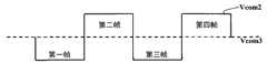
图11是根据本发明第二实施例的1/2屏插黑的示意图。Fig. 11 is a schematic diagram of a 1/2 screen plug-in black according to the second embodiment of the present invention.
图12是图11的实现方式示意图。FIG. 12 is a schematic diagram of an implementation in FIG. 11 .
具体实施方式Detailed ways
以下将参照附图来详细说明本发明的示例性实施例。Exemplary embodiments of the present invention will be described in detail below with reference to the accompanying drawings.
以下实施例是以液晶显示装置在采用点反转驱动方式时进行详细描述的,但本发明实施例并不局限于此,例如,本发明实施例的液晶显示装置亦可采用列反转驱动方式,只要不脱离本发明的实质所做的任何改动均应被包括在本发明的权利要求的保护范围之内。The following embodiments are described in detail when the liquid crystal display device adopts the dot inversion driving method, but the embodiments of the present invention are not limited thereto, for example, the liquid crystal display device of the embodiment of the present invention can also adopt the column inversion driving method , as long as it does not deviate from the essence of the present invention, any modification should be included in the scope of protection of the claims of the present invention.
首先参照图6至图10B来说明本发明的第一实施例。本发明第一实施例的液晶显示装置包括一液晶面板,液晶面板包括阵列基板和彩色滤光片基板(也称对置基板)。First, a first embodiment of the present invention will be described with reference to FIGS. 6 to 10B. The liquid crystal display device according to the first embodiment of the present invention includes a liquid crystal panel, and the liquid crystal panel includes an array substrate and a color filter substrate (also called an opposite substrate).
如图7所示,液晶面板通常包括多个像素单元10,并且在阵列基板侧 设置数据线D1、D2、D3…和扫描线G1、G2、G3…。每个像素单元10包括薄膜晶体管101、液晶电容CLC及存储电容Cst(Cst1或者Cst2)。存储电容Cst的第一端为像素电极102,第二端为阵列基板上的公共电极103、104(即第一公共电极,或称为存储电极)。液晶电容CLC的第一端为像素电极102,第二端为对置基板上的公共电极105(即第二公共电极,或称为对置电极)。扫描线中的单条扫描线电连接相邻两行像素单元中的奇数列像素单元或偶数列像素单元。相邻两行像素单元中的奇数列像素单元或偶数列像素单元中的薄膜晶体管101的栅极101g与扫描线(G1、G2…)连接,以接收扫描线所传输的扫描信号。奇数据线(D1、D3…)连接当前帧为所有正极性的像素单元10,称为第一像素单元,偶数据线(D2、D4…)连接当前帧为所有负极性的像素单元10,称为第二像素单元。第一像素单元中存储电容Cst1的第二端即第一公共电极103通过第一公共线106电性连接,第一公共线106用以接收第一公共电压信号Vcom1(如图6所示),第二像素单元中存储电容Cst2的第二端即第一公共电极104通过第二公共线108电性连接,第二公共线108用以接收第二公共电压信号Vcom2(如图6所示)。像素电极102通过薄膜晶体管101的漏极101d和源极101s而与数据线(D1、D2…)耦接。多个像素单元中液晶电容CLC的第二端即第二公共电极105电性连接以接收第三公共电压信号Vcom3。在本实施例中,第一、第二公共电压信号Vcom1、Vcom2是交流电压信号。第三公共电压信号Vcom3是直流电压。As shown in Fig. 7, a liquid crystal panel usually includes a plurality of pixel units 10, and data lines D1, D2, D3... and scan lines G1, G2, G3... are arranged on the side of the array substrate. Each pixel unit 10 includes a
液晶显示装置采用列反转驱动时的液晶面板的连接方式与上述采用点反转驱动时所不同的是:扫描线中的单条扫描线电连接同一行像素单元的所有像素单元。其他连接方式与上述采用点反转驱动时的液晶面板的连接方式类似,故在这里不再赘述。The connection mode of the liquid crystal panel when the liquid crystal display device adopts the column inversion driving is different from the above-mentioned dot inversion driving in that a single scanning line in the scanning line is electrically connected to all the pixel units of the same row of pixel units. Other connection methods are similar to the above-mentioned connection methods of the liquid crystal panel when dot inversion driving is adopted, so details will not be repeated here.
参照图8A和图8B,其分别是根据本发明第一实施例的奇数据线和偶数据线上连接的像素单元的第一、第二公共电压信号Vcom1、Vcom2的波形图。第一公共电压信号Vcom1和第二公共电压信号Vcom2在同一帧中电压幅值相同但极性相反(即,当第一公共电压信号Vcom1为高电平时第二公共电压信号Vcom2为低电平;当第一公共电压信号Vcom1为低电平 时第二公共电压信号Vcom2为高电平)。Referring to FIG. 8A and FIG. 8B , they are respectively waveform diagrams of the first and second common voltage signals Vcom1 and Vcom2 of the pixel units connected to the odd data line and the even data line according to the first embodiment of the present invention. The first common voltage signal Vcom1 and the second common voltage signal Vcom2 have the same voltage amplitude but opposite polarities in the same frame (that is, when the first common voltage signal Vcom1 is high level, the second common voltage signal Vcom2 is low level; When the first common voltage signal Vcom1 is at low level, the second common voltage signal Vcom2 is at high level).
以下参照图9A和图9B来说明本发明第一实施例的像素单元在被驱动时,其像素电压、数据信号电压、公共电压信号和扫描信号的波形。在图9A和图9B中,Vgh代表扫描线的高电压(也称为扫描开启信号),Vgl代表扫描线的低电压,Vsig1、Vsig2代表提供给数据线上的数据信号电压,Vpixel代表像素电极102充电的电压(即像素电压),Vcom3代表提供给像素单元10中液晶电容CLC的公共电极105(即第二公共电极)的第三公共电压信号,Vcom1、Vcom2分别代表提供给奇数据线和偶数据线上连接的像素单元10中存储电容Cst1、Cst2的公共电极103、104(即第一公共电极)的第一、第二公共电压信号。The waveforms of pixel voltage, data signal voltage, common voltage signal and scanning signal when the pixel unit of the first embodiment of the present invention is driven will be described below with reference to FIG. 9A and FIG. 9B . In FIG. 9A and FIG. 9B, Vgh represents the high voltage of the scan line (also called the scan-on signal), Vgl represents the low voltage of the scan line, Vsig1 and Vsig2 represent the data signal voltage supplied to the data line, and Vpixel represents the
图9A和图9B分别为本发明第一实施例的奇数据线和偶数据线上连接的某像素单元的像素电压、数据信号电压、第一公共电压信号和扫描信号的波形图。为了简单起见,图9A和图9B仅示出了关于第n帧和第n+1帧的波形。在液晶面板工作时,第一、第二公共电压信号Vcom1、Vcom2比扫描开启信号Vgh提前t时间输入,即在薄膜晶体管101开启之前的t时间输入第一、第二公共电压信号Vcom1、Vcom2,并且t>Ton(Ton为像素电极从最小电压到最大电压的充电时间),第一公共电压信号Vcom1与薄膜晶体管101开启后输入到第一像素单元上的数据信号电压Vsig1具有相同极性(即第一公共电压信号Vcom1与数据信号电压Vsig1同为高电平或低电平),第二公共电压信号Vcom2与薄膜晶体管101开启后输入到第二像素单元上的数据信号电压Vsig2具有相同极性(即第二公共电压信号Vcom2与数据信号电压Vsig2同为高电平或低电平)。液晶显示装置的黑白响应时间Tresponse包括像素电极102从最小电压到最大电压的充电时间Ton和像素电极102从最大电压到最小电压的时间Toff,并且Toff>Ton。例如,当使用黑白响应时间为5ms的液晶显示装置时,像素电极102从最小电压到最大电压的充电时间Ton<2ms,在这种情况下,可以取t=2ms。9A and 9B are waveform diagrams of the pixel voltage, data signal voltage, first common voltage signal and scanning signal of a pixel unit connected to the odd data line and the even data line in the first embodiment of the present invention, respectively. For the sake of simplicity, FIGS. 9A and 9B only show waveforms about the nth frame and the n+1th frame. When the liquid crystal panel is working, the first and second common voltage signals Vcom1 and Vcom2 are input t time earlier than the scan-on signal Vgh, that is, the first and second common voltage signals Vcom1 and Vcom2 are input t time before the
如图9A所示,对于第n帧,在薄膜晶体管101开启之前的t时间,第一公共电压信号Vcom1开始输入,由于电容耦合效应,像素电极102产生一个耦合电压Vdrop,Vdrop由下式得出:As shown in FIG. 9A, for the nth frame, the first common voltage signal Vcom1 starts to be input at the time t before the
Vdrop=ΔVcom1×Cst/(CLC+Cst +Cgs),(1)Vdrop =ΔVcom1×Cst /(CLC +Cst +Cgs ), (1)
其中ΔVcom1为第一公共电压信号Vcom1的变化值(即当Vcom1从最小值Vcom1min变为最大值Vcom1max时,ΔVcom1=Vcom1max-Vcom1min,当Vcom1从最大值Vcom1max变为最小值Vcom1min时,ΔVcom1=Vcom1min-Vcom1max),CLC为液晶电容,Cst为存储电容,Cgs为TFT的栅极与源极之间的电容。Where ΔVcom1 is the change value of the first common voltage signal Vcom1 (that is, when Vcom1 changes from the minimum value Vcom1min to the maximum value Vcom1max , ΔVcom1=Vcom1max -Vcom1min , when Vcom1 changes from the maximum value Vcom1max to the minimum value Vcom1min , ΔVcom1=Vcom1min -Vcom1max ), CLC is the liquid crystal capacitance, Cst is the storage capacitance, and Cgs is the capacitance between the gate and the source of the TFT.
在对像素电极102充电之前,即第n帧的扫描开启信号来临之前,像素单元10具有一耦合电压Vdrop。耦合后的像素电压Vcoupled为第n-1帧的像素电压与耦合电压Vdrop之和。如图9A所示,对于第n帧,在对像素电极102充电之前,由于第一公共电压信号Vcom1从最小值Vcom1min转变为最大值Vcom1max,由式(1)可知,此时Vdrop为正电压,因此耦合后的像素电压Vcoupled增大,即耦合电压Vdrop已将像素电极102从负极性拉向正极性。因此,当在对像素电极102充电时,像素电极102只需从正极性的电压变为正极性的电压,而不需要像现有技术需从负极性的电压变为正极性的电压,故减小了像素电极102变化的电压差,因此,具有预充电功能。Before charging the
在上述t时间之后,扫描线被施加第n帧的扫描开启信号,扫描信号的高电压Vgh使连接于该扫描线上的薄膜晶体管101处于导通状态,即,薄膜晶体管101的漏极101d与源极101s导通。在此期间,代表第n帧像素电压的数据信号电压Vsig1藉数据线通过薄膜晶体管101的源极101s和漏极101d施加至像素电极102,使该扫描线上连接的像素单元10从耦合后的像素电压Vcoupled变换到第n帧的像素电压Vpixel,并使该扫描线上连接的像素单元中的存储电容Cst处于充电状态,且由存储电容在第n帧的时间内保持该像素电压Vpixel。理论上,在第n+1帧的扫描开启信号施加至该扫描线之前,该扫描线上连接的像素单元10显示的像素电压Vpixel保持不变。但实际上,当扫描信号从高电压Vgh转变为低电压Vgl瞬间,薄膜晶体管101截止,液晶电容CLC藉由存储电容Cst而维持的充电电压会由于电容耦合效应而突然有所下降,并且在扫描信号保持为低电压Vgl之后会由于邻近的寄生电阻的影响而有少许减小。After the above-mentioned t time, the scanning line is applied with the scan-on signal of the nth frame, and the high voltage Vgh of the scanning signal makes the thin-
在第n+1帧的扫描开启信号施加至该扫描线时,该扫描线上连接的像素单元的极性发生反转。与第n帧类似,在薄膜晶体管101开启之前的t时间,第一公共电压信号Vcom1从最大值Vcom1max转变为最小值Vcom1min,由于电容耦合效应,像素电极102产生一个耦合电压Vdrop,该Vdrop同样由式(1)得出。When the scan-on signal of the (n+1)th frame is applied to the scan line, the polarity of the pixel units connected to the scan line is reversed. Similar to the nth frame, the first common voltage signal Vcom1 changes from the maximum value Vcom1max to the minimum value Vcom1min at time t before the
与第n帧类似,耦合后的像素电压Vcoupled为第n帧的像素电压与耦合电压Vdrop之和。如图9A所示,对于第n+1帧,在对像素电极102充电之前,由于第一公共电压信号Vcom1从最大值Vcom1max转变为最小值Vcom1min,由式(1)可知,此时Vdrop为负电压,因此耦合后的像素电压Vcoupled减小,即耦合电压Vdrop已将像素电极102从正极性拉向负极性,因此,当在对像素电极102充电时,像素电极102只需从负极性的电压变为负极性的电压,而不需要像现有技术需从正极性的电压变为负极性的电压,故减小了像素电极102变化的电压差,因此,具有预充电功能。Similar to the nth frame, the coupled pixel voltage Vcoupled is the sum of the pixel voltage in the nth frame and the coupling voltage Vdrop . As shown in FIG. 9A , for the n+1th frame, before the
在t时间之后,在第n+1帧的扫描开启信号施加至该扫描线期间,扫描信号的高电压Vgh使连接于该扫描线上的薄膜晶体管101都处于导通状态,同时,代表第n+1帧像素电压的数据信号电压Vsig1藉数据线通过薄膜晶体管101的源极101s和漏极101d施加至像素电极,使该扫描线上连接的像素单元10从耦合后的像素电压Vcoupled变换到第n+1帧像素电压Vpixel,并使像素单元10中的存储电容Cst处于充电状态。在薄膜晶体管关闭后,由存储电容Cst保持第n+1帧像素电压Vpixel。同样,实际上,当扫描信号从高电压Vgh转变为低电压Vgl瞬间,薄膜晶体管101截止,液晶电容CLC藉由存储电容Cst而维持的充电电压会由于电容耦合效应而突然有所下降,并且在扫描信号保持为低电压Vgl之后会由于邻近的寄生电阻的影响而有少许减小。如此,周而复始。After time t, when the scan-on signal of the n+1th frame is applied to the scan line, the high voltage Vgh of the scan signal makes all the
图9B为偶数据线上连接的某像素单元的像素电压、数据信号电压、第二公共电压信号和扫描信号的波形图。因为偶数据线上连接的第二像素单元与奇数据线上连接的第一像素单元在同一帧内的极性相反,且第一公共电压信号和第二公共电压信号在同一帧内的极性相反,所以偶数据线上连接的第二像素单元的像素电压和第二公共电压信号的波形图分别与奇数 据线上连接的第一像素单元的像素电压和第一公共电压信号的波形图相反。由于在此情况下通过对图9A的描述可以清楚地理解图9B,因此这里不再赘述。9B is a waveform diagram of a pixel voltage, a data signal voltage, a second common voltage signal and a scanning signal of a pixel unit connected to an even data line. Because the polarity of the second pixel unit connected on the even data line is opposite to that of the first pixel unit connected on the odd data line in the same frame, and the polarities of the first common voltage signal and the second common voltage signal in the same frame On the contrary, the pixel voltage of the second pixel unit connected on the even data line and the waveform diagram of the second common voltage signal are respectively opposite to the waveform diagram of the pixel voltage of the first pixel unit connected on the odd data line and the first common voltage signal . Since FIG. 9B can be clearly understood through the description of FIG. 9A in this case, details are not repeated here.
以下将参照图10A和图10B来说明根据本发明第一实施例的液晶面板的驱动仿真情况。由于实际仿真仪器和条件的局限,因此在这里将基于60Hz、900条扫描线的单条扫描线时间来仿真12条扫描线。The driving simulation of the liquid crystal panel according to the first embodiment of the present invention will be described below with reference to FIGS. 10A and 10B . Due to the limitations of actual simulation instruments and conditions, 12 scan lines will be simulated here based on a single scan line time of 60 Hz and 900 scan lines.
参照图10A,其示出本发明第一实施例的液晶面板在一种情况下的驱动仿真图,该仿真图是在以下参数时取得的:扫描信号的高电压Vgh=20V,扫描信号的低电压Vgl=-10V;数据信号的高电压Vdh1=6.7V,数据信号的低电压Vdl1=6.3V(此处的数据信号电压对应于256级的亮度灰阶中的最亮灰阶L255的电压,即输入白色电压信号的情况);TFT的长度=4.5μm,TFT的宽度=31.7μm;存储电容Cst=346.67fF,TFT的栅极与源极之间的电容Cgs=28.96fF,液晶电容CLC=273.355fF;第一公共电压信号的最大值Vcom1max=10V,第一公共电压信号的最小值Vcom1min=-10V,第三公共电压信号Vcom3=4.965V。Referring to FIG. 10A , it shows a driving simulation diagram of the liquid crystal panel of the first embodiment of the present invention under one condition. The simulation diagram is obtained under the following parameters: the high voltage of the scanning signal Vgh=20V, the low voltage of the scanning signal Voltage Vgl=-10V; the high voltage Vdh1=6.7V of the data signal, the low voltage Vdl1=6.3V of the data signal (the voltage of the data signal here corresponds to the voltage of the brightest grayscale L255 in the 256-level brightness grayscale, That is, the case of inputting a white voltage signal); the length of the TFT = 4.5 μm, the width of the TFT = 31.7 μm; the storage capacitor Cst = 346.67fF, the capacitance Cgs between the gate and the source of the TFT = 28.96fF, and the liquid crystal capacitance CLC =273.355fF; the maximum value of the first common voltage signal Vcom1max =10V, the minimum value of the first common voltage signal Vcom1min =-10V, and the third common voltage signal Vcom3 =4.965V.
第n-1帧的像素电压为5.17V。在第n帧的扫描开启信号施加至扫描线之前的t时间,第一公共电压信号Vcom1从10V变为-10V,由于电容耦合,像素电极产生一个耦合电压Vdrop,如图10A所示,Vdrop为-10.66V,因此耦合后的像素电压为5.17-10.66=-5.49V,耦合后的像素电压与第三公共电压信号Vcom3之间的电压差(即,液晶电容的电压)为4.965-(-5.49)=10.455V。The pixel voltage of the n-1th frame is 5.17V. At time t before the scan-on signal of the nth frame is applied to the scan line, the first common voltage signal Vcom1 changes from 10V to -10V. Due to capacitive coupling, the pixel electrode generates a coupling voltage Vdrop , as shown in FIG. 10A , VThe drop is -10.66V, so the coupled pixel voltage is 5.17-10.66=-5.49V, and the voltage difference between the coupled pixel voltage and the third common voltage signal Vcom3 (that is, the voltage of the liquid crystal capacitor) is 4.965-( -5.49) = 10.455V.
在t时间之后,扫描线被施加第n帧的扫描开启信号,扫描信号的高电压Vgh使连接于该扫描线上的薄膜晶体管处于导通状态。在此期间,代表第n帧像素电压的数据信号的低电压Vdl1藉数据线通过薄膜晶体管的源极和漏极施加至像素电极,使该扫描线上连接的像素单元从耦合后的像素电压Vcoupled-5.49V变换到数据信号的低电压6.3V,并使该扫描线上连接的像素单元中的存储电容处于充电状态。当扫描信号从高电压Vgh转变为低电压Vgl瞬间,薄膜晶体管截止,液晶电容藉由存储电容而维持的充电电压会由于电容耦合效应而突然下降,产生一馈通电压6.3-4.76=1.54V, 在此之后保持为4.76V。After time t, the scan line is applied with the scan start signal of the nth frame, and the high voltage Vgh of the scan signal turns on the thin film transistor connected to the scan line. During this period, the low voltage Vdl1 of the data signal representing the pixel voltage of the nth frame is applied to the pixel electrode through the data line through the source and drain of the thin-film transistor, so that the pixel unit connected to the scanning line is converted from the coupled pixel voltage VThe coupled -5.49V is converted to the low voltage 6.3V of the data signal, and the storage capacitor in the pixel unit connected to the scanning line is charged. When the scan signal changes from a high voltage Vgh to a low voltage Vgl, the thin film transistor is turned off, and the charging voltage maintained by the liquid crystal capacitor through the storage capacitor will suddenly drop due to the capacitive coupling effect, resulting in a feed-through voltage of 6.3-4.76=1.54V, After that it remains at 4.76V.
在第n+1帧的扫描开启信号施加至该扫描线之前的t时间,第一公共电压信号Vcom1从-10V变为10V,由于电容耦合,像素电极产生一个耦合电压Vdrop,如图10A所示,Vdrop为-10.66V,因此耦合后的像素电压Vcoupled为4.76+10.66=15.42V,耦合后的像素电压Vcoupled与第三公共电压信号Vcom3之间的电压差(即,液晶电容的电压)为15.42-4.965=10.455V。At time t before the scan-on signal of the n+1th frame is applied to the scan line, the first common voltage signal Vcom1 changes from -10V to 10V, and the pixel electrode generates a coupled voltage Vdrop due to capacitive coupling, as shown in FIG. 10A As shown, Vdrop is -10.66V, so the coupled pixel voltage Vcoupled is 4.76+10.66=15.42V, and the voltage difference between the coupled pixel voltage Vcoupled and the third common voltage signal Vcom3 (that is, the liquid crystal capacitance Voltage) is 15.42-4.965=10.455V.
在t时间之后,扫描线被施加第n+1帧的扫描开启信号,扫描信号的高电压Vgh使连接于该扫描线上的薄膜晶体管处于导通状态。在此期间,代表第n+1帧像素电压的数据信号的高电压Vdh1藉数据线通过薄膜晶体管的源极和漏极施加至像素电极,使该扫描线上连接的像素单元从耦合后的像素电压Vcoupled15.42V变换到数据信号的高电压6.7V,并使该扫描线上连接的像素单元中的存储电容处于充电状态。当扫描信号从高电压Vgh转变为低电压Vgl瞬间,薄膜晶体管截止,液晶电容藉由存储电容而维持的充电电压会由于电容耦合效应而突然下降,产生一馈通电压6.7-5.17=1.53V,在此之后保持为5.17V。如此,周而复始。After time t, the scanning line is applied with the scan-on signal of the n+1th frame, and the high voltage Vgh of the scanning signal makes the thin film transistor connected to the scanning line in a conducting state. During this period, the high voltage Vdh1 of the data signal representing the pixel voltage of the n+1th frame is applied to the pixel electrode through the data line through the source and drain of the thin film transistor, so that the pixel unit connected on the scanning line is connected to the pixel after coupling. The voltage Vcoupled 15.42V is transformed into the high voltage 6.7V of the data signal, and the storage capacitor in the pixel unit connected to the scanning line is charged. When the scan signal changes from a high voltage Vgh to a low voltage Vgl, the thin film transistor is turned off, and the charging voltage maintained by the liquid crystal capacitor through the storage capacitor will suddenly drop due to the capacitive coupling effect, resulting in a feed-through voltage of 6.7-5.17=1.53V, After that it remains at 5.17V. So, again and again.
由此可见,在图10A的情况下,耦合后的像素电压Vcoupled分别为-5.49V和15.42V,这两个电压值分别与第三公共电压信号Vcom3(Vcom3=4.965V)的电压差均为10.455V,大于6V,因此在采用最暗灰阶对应的压差为6V的液晶显示装置的情况下,当输入为白色电压信号(即,最亮级别信号)时,像素单元具有很好的插黑效果。It can be seen that, in the case of FIG. 10A , the coupled pixel voltages Vcoupled are -5.49V and 15.42V respectively, and the voltage differences between these two voltage values and the third common voltage signal Vcom3 (Vcom3=4.965V) are equal. is 10.455V, which is greater than 6V. Therefore, in the case of a liquid crystal display device whose voltage difference corresponding to the darkest gray scale is 6V, when the input is a white voltage signal (that is, the brightest level signal), the pixel unit has a good Insert black effect.
参照图10B,其示出本发明第一实施例的液晶面板在另一种情况下的驱动仿真图,该仿真图是在以下参数时取得的:扫描信号的高电压Vgh=20V,扫描信号的低电压Vgl=-10V;数据信号的高电压Vdh2=13.2V,数据信号的低电压Vdl2=0.2V(此处的数据信号电压对应于256级的亮度灰阶中的最暗灰阶L0的电压,即输入黑色电压信号的情况);TFT的长度=4.5μm,TFT的宽度=31.7μm;存储电容Cst=346.67fF,TFT的栅极与源极之间的电容Cgs=28.96fF,液晶电容CLC=273.355fF;第一公共电压信号的最大值Vcom1max=10V,第一公共电压信号的最小值 Vcom1min=-10V,第三公共电压信号Vcom3=5.17V。Referring to Fig. 10B, it shows the driving simulation diagram of the liquid crystal panel of the first embodiment of the present invention in another case, the simulation diagram is obtained under the following parameters: the high voltage Vgh of the scanning signal = 20V, the scanning signal Low voltage Vgl=-10V; high voltage Vdh2=13.2V of the data signal, low voltage Vdl2=0.2V of the data signal (the data signal voltage here corresponds to the voltage of the darkest grayscale L0 in the 256-level brightness grayscale , that is, the case of inputting a black voltage signal); the length of the TFT=4.5 μm, the width of the TFT=31.7 μm; the storage capacitance Cst =346.67fF, the capacitance Cgs between the gate and the source of the TFT =28.96fF, the liquid crystal Capacitance CLC =273.355fF; the maximum value of the first common voltage signal Vcom1max =10V, the minimum value of the first common voltage signal Vcom1min =-10V, and the third common voltage signal Vcom3 =5.17V.
第n-1帧的像素电压为11.74V。在第n帧的扫描开启信号施加至扫描线之前的t时间,第一公共电压信号Vcom1从10V变为-10V,由于电容耦合,像素电极产生一个耦合电压Vdrop,如图10A所示,Vdrop为-10.66V,因此耦合后的像素电压Vcoupled为11.74-10.66=1.08V,耦合后的像素电压Vcoupled与第三公共电压信号Vcom3之间的电压差(即,液晶电容的电压)为5.17-1.08=4.09V。The pixel voltage of the n-1th frame is 11.74V. At time t before the scan-on signal of the nth frame is applied to the scan line, the first common voltage signal Vcom1 changes from 10V to -10V. Due to capacitive coupling, the pixel electrode generates a coupling voltage Vdrop , as shown in FIG. 10A , Vdrop is -10.66V, so the coupled pixel voltage Vcoupled is 11.74-10.66=1.08V, and the voltage difference between the coupled pixel voltage Vcoupled and the third common voltage signal Vcom3 (that is, the voltage of the liquid crystal capacitor) is 5.17-1.08 = 4.09V.
在t时间之后,扫描线被施加第n帧的扫描开启信号,扫描信号的高电压Vgh使连接于该扫描线上的薄膜晶体管处于导通状态。在此期间,代表第n帧像素电压的数据信号的低电压Vdl2藉数据线通过薄膜晶体管的源极和漏极施加至像素电极,使该扫描线上连接的像素单元从耦合后的像素电压Vcoupled1.08V变换到数据信号的低电压0.2V,并使该扫描线上连接的像素单元中的存储电容处于充电状态。当扫描信号从高电压Vgh转变为低电压Vgl瞬间,薄膜晶体管截止,液晶电容藉由存储电容而维持的充电电压会由于电容耦合效应而突然下降,产生一馈通电压0.2-(-1.4)=1.6V,在此之后保持为-1.4V。After time t, the scan line is applied with the scan start signal of the nth frame, and the high voltage Vgh of the scan signal turns on the thin film transistor connected to the scan line. During this period, the low voltage Vdl2 of the data signal representing the pixel voltage of the nth frame is applied to the pixel electrode through the data line through the source and drain of the thin film transistor, so that the pixel unit connected to the scanning line is converted from the coupled pixel voltage VThe coupled 1.08V is converted to the low voltage 0.2V of the data signal, and the storage capacitor in the pixel unit connected to the scanning line is charged. When the scan signal changes from a high voltage Vgh to a low voltage Vgl, the thin film transistor is turned off, and the charging voltage maintained by the liquid crystal capacitor through the storage capacitor will suddenly drop due to the capacitive coupling effect, resulting in a feed-through voltage of 0.2-(-1.4)= 1.6V and stay at -1.4V after that.
在第n+1帧的扫描开启信号施加至该扫描线之前的t时间,第一公共电压信号Vcom1从-10V变为10V,由于电容耦合,像素电极产生一个耦合电压Vdrop,如图10A所示,Vdrop为-10.66V,因此耦合后的像素电压Vcoupled为-1.4+10.66=9.26V,耦合后的像素电压Vcoupled与第三公共电压信号Vcom3之间的电压差(即,液晶电容的电压)为9.26-5.17=4.09V。At time t before the scan-on signal of the n+1th frame is applied to the scan line, the first common voltage signal Vcom1 changes from -10V to 10V, and the pixel electrode generates a coupled voltage Vdrop due to capacitive coupling, as shown in FIG. 10A As shown, Vdrop is -10.66V, so the coupled pixel voltage Vcoupled is -1.4+10.66=9.26V, and the voltage difference between the coupled pixel voltage Vcoupled and the third common voltage signal Vcom3 (that is, the liquid crystal capacitance The voltage) is 9.26-5.17=4.09V.
在t时间之后,扫描线被施加第n+1帧的扫描开启信号,扫描信号的高电压Vgh使连接于该扫描线上的薄膜晶体管处于导通状态。在此期间,代表第n+1帧像素电压的数据信号的高电压Vdh2藉数据线通过薄膜晶体管的源极和漏极施加至像素电极,使该扫描线上连接的像素单元从耦合后的像素电压Vcoupled9.26V变换到数据信号的高电压13.2V,并使该扫描线上连接的像素单元中的存储电容处于充电状态。当扫描信号从高电压Vgh转变为低电压Vgl瞬间,薄膜晶体管截止,液晶电容藉由存储电容而维持 的充电电压会由于电容耦合效应而突然下降,产生一馈通电压13.2-11.74=1.46V,在此之后保持为11.74V。如此,周而复始。After time t, the scan line is applied with the scan start signal of the (n+1)th frame, and the high voltage Vgh of the scan signal makes the thin film transistor connected to the scan line in a conduction state. During this period, the high voltage Vdh2 of the data signal representing the pixel voltage of the n+1th frame is applied to the pixel electrode through the data line through the source and drain of the thin film transistor, so that the pixel unit connected on the scanning line is connected from the coupled pixel The voltage Vcoupled 9.26V is transformed into the high voltage 13.2V of the data signal, and the storage capacitor in the pixel unit connected to the scanning line is charged. When the scan signal changes from a high voltage Vgh to a low voltage Vgl, the thin film transistor is turned off, and the charging voltage maintained by the liquid crystal capacitor through the storage capacitor will suddenly drop due to the capacitive coupling effect, resulting in a feed-through voltage of 13.2-11.74=1.46V, After that it remains at 11.74V. So, again and again.
由此可见,在图10B所示的情况下,耦合后的像素电压Vcoupled分别为1.08V和9.26V,这两个电压值分别与第三公共电压信号Vcom3(Vcom3=5.17V)的电压差均为4.09V,小于6V,因此在采用最暗灰阶对应的压差为6V的液晶显示装置的情况下,当输入为黑色电压信号(即,最暗级别信号)时,像素单元仅具有插灰效果。It can be seen that, in the situation shown in FIG. 10B , the coupled pixel voltages Vcoupled are respectively 1.08V and 9.26V, and the voltage difference between these two voltage values and the third common voltage signal Vcom3 (Vcom3=5.17V) Both are 4.09V, which is less than 6V. Therefore, in the case of a liquid crystal display device with a voltage difference of 6V corresponding to the darkest gray scale, when the input is a black voltage signal (that is, the darkest level signal), the pixel unit only has an interpolation signal. gray effect.
因此,本发明通过在扫描开启施加至扫描线之前使得像素电极具有易耦合电压Vdrop,从而在不需要提高驱动频率的情况下,实现良好的插黑或插灰效果。Therefore, the present invention enables the pixel electrode to have the easy-coupling voltage Vdrop before the scan-on is applied to the scan line, so as to achieve a good effect of black insertion or gray insertion without increasing the driving frequency.
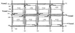
以下将参照图11至图12来说明本发明的第二实施例。为了提高显示亮度,本发明第二实施例可以不实行全屏插黑,而采用部分屏幕的滚动插黑,如1/2屏插黑、1/3屏插黑等,只需稍微改变一下本发明的设计即可实现部分屏幕的插黑。图11是根据本发明第二实施例的1/2屏插黑的示意图。如图11所示,第n-1帧与第n帧之间插黑上半屏,第n帧与第n+1帧之间插黑下半屏,依此半屏滚动插黑。图11的实现方式如图12所示,将1/2屏以上的奇数据线和偶数据线所连接的第一和第二像素单元的第一公共电极分别接第一和第二公共电压信号Vcom1和Vcom2,而1/2屏以下的奇数据线和偶数据线所连接的第一和第二像素单元的第一公共电极分别接第四和第五公共电压信号Vcom1’和Vcom2’,通过控制Vcom1和Vcom2以及Vcom1’和Vcom2’的输入时间即可实现1/2屏插黑。A second embodiment of the present invention will be described below with reference to FIGS. 11 to 12 . In order to improve the display brightness, the second embodiment of the present invention does not implement full-screen black insertion, but uses rolling black insertion of part of the screen, such as 1/2 screen black insertion, 1/3 screen black insertion, etc., only need to slightly change the present invention The design can realize the black insertion of part of the screen. Fig. 11 is a schematic diagram of a 1/2 screen plug-in black according to the second embodiment of the present invention. As shown in Figure 11, the upper half screen of black is inserted between the n-1th frame and the nth frame, and the lower half of the black screen is inserted between the nth frame and the n+1th frame. The implementation of Figure 11 is shown in Figure 12, the first common electrodes of the first and second pixel units connected to the odd data lines and even data lines above 1/2 screen are respectively connected to the first and second common voltage signals Vcom1 and Vcom2, and the first common electrodes of the first and second pixel units connected to the odd data lines and even data lines below the 1/2 screen are respectively connected to the fourth and fifth common voltage signals Vcom1' and Vcom2', through Controlling the input time of Vcom1 and Vcom2 and Vcom1' and Vcom2' can realize 1/2 screen black insertion.
如图12所示,本发明第二实施例的液晶面板的像素单元包括第一组像素单元和第二组像素单元。第一组像素单元中的第一像素单元的第一公共电极电性连接以接收第一公共电压信号Vcom1,第一组像素单元中的第二像素单元的第一公共电极电性连接以接收第二公共电压信号Vcom2;第二组像素单元中的第一像素单元的第一公共电极电性连接以接收第四公共电压信号Vcom1’,第二组像素单元中的第二像素单元的第一公共电极电性连接以接收第五公共电压信号Vcom2’。另外,这两组中的像素单元的第二公共电极电性连接以接收第三公共电压信号Vcom3。第一和第二公共 电压信号Vcom1和Vcom2为交流电压信号且在同一帧内电压幅值相同极性相反;第四和第五公共电压信号Vcom1’和Vcom2’为交流电压信号且在同一帧内电压幅值相同极性相反。这样,与第一实施例类似,可以通过第一和第二公共电压信号Vcom1和Vcom2来对第一组像素单元中的像素单元进行插黑和预充电,并且可以通过第四和第五公共电压信号Vcom1’和Vcom2’来对第二组像素单元中的像素单元进行插黑和预充电。此外,通过设置第一和第四公共电压信号Vcom1和Vcom1’使其仅时序不同并且设置第二和第五公共电压信号Vcom2和Vcom2’使其仅时序不同,可以实现以不同的时序对第一组像素单元和第二组像素单元进行插黑。例如,使第一和第二公共电压信号Vcom1和Vcom2在奇数帧内比扫描开启信号提前t时间输入,且第四和第五公共电压信号Vcom1’和Vcom2’在偶数帧内比扫描开启信号提前t时间输入。在这种情况下,可以在奇数帧内对第一组像素单元进行插黑,在偶数帧内对第二组像素单元进行插黑,从而实现部分屏幕的滚动插黑。As shown in FIG. 12 , the pixel units of the liquid crystal panel according to the second embodiment of the present invention include a first group of pixel units and a second group of pixel units. The first common electrode of the first pixel unit in the first group of pixel units is electrically connected to receive the first common voltage signal Vcom1, and the first common electrode of the second pixel unit in the first group of pixel units is electrically connected to receive the first common voltage signal Vcom1. Two common voltage signal Vcom2; the first common electrode of the first pixel unit in the second group of pixel units is electrically connected to receive the fourth common voltage signal Vcom1', the first common electrode of the second pixel unit in the second group of pixel units The electrodes are electrically connected to receive the fifth common voltage signal Vcom2'. In addition, the second common electrodes of the pixel units in the two groups are electrically connected to receive the third common voltage signal Vcom3. The first and second common voltage signals Vcom1 and Vcom2 are AC voltage signals and have the same voltage amplitude and opposite polarity in the same frame; the fourth and fifth common voltage signals Vcom1' and Vcom2' are AC voltage signals and are in the same frame The same voltage amplitude and opposite polarity. In this way, similar to the first embodiment, the pixel units in the first group of pixel units can be black inserted and precharged through the first and second common voltage signals Vcom1 and Vcom2, and the fourth and fifth common voltage signals can be used to Signals Vcom1' and Vcom2' are used to insert black and precharge the pixel units in the second group of pixel units. In addition, by setting the first and fourth common voltage signals Vcom1 and Vcom1' so that only the timing is different and setting the second and fifth common voltage signals Vcom2 and Vcom2' so that only the timing is different, it is possible to implement different timings for the first The first group of pixel units and the second group of pixel units perform black insertion. For example, the first and second common voltage signals Vcom1 and Vcom2 are input t time earlier than the scan-on signal in odd frames, and the fourth and fifth common voltage signals Vcom1' and Vcom2' are earlier than the scan-on signal in even frames. t time input. In this case, black insertion can be performed on the first group of pixel units in odd frames, and black insertion can be performed on the second group of pixel units in even frames, so as to realize rolling black insertion of part of the screen.
由于除了增加了第四和第五公共电压信号Vcom1’和Vcom2’之外,本发明第二实施例的具体结构与第一实施例相同,因此这里不再赘述。Since the specific structure of the second embodiment of the present invention is the same as that of the first embodiment except for the addition of the fourth and fifth common voltage signals Vcom1' and Vcom2', details will not be repeated here.
以上是以1/2屏插黑为例进行详细说明,但本发明并不局限于此,本发明实施例的液晶面板的像素单元亦可包括第三组像素单元,或者,亦可包括第三组像素单元和第四组像素单元等。例如,当进行1/3屏插黑时,本发明实施例的液晶面板的像素单元包括三组像素单元,即第一组像素单元、第二组像素单元及第三组像素单元;或者,当进行1/4屏插黑时,本发明实施例的液晶面板的像素单元包括四组像素单元,即第一组像素单元、第二组像素单元、第三组像素单元及第四组像素单元;当进行1/n屏插黑时,本发明实施例的液晶面板的像素单元包括n组像素单元,即第一组像素单元、第二组像素单元、第三组像素单元......、第n-1组像素单元及第n组像素单元。The above is described in detail by taking 1/2 screen black as an example, but the present invention is not limited thereto. The pixel unit of the liquid crystal panel in the embodiment of the present invention may also include a third group of pixel units, or may also include a third group of pixel units. The first group of pixel units and the fourth group of pixel units, etc. For example, when 1/3 of the screen is inserted black, the pixel unit of the liquid crystal panel in the embodiment of the present invention includes three groups of pixel units, that is, the first group of pixel units, the second group of pixel units and the third group of pixel units; or, when When performing 1/4 screen black insertion, the pixel unit of the liquid crystal panel in the embodiment of the present invention includes four groups of pixel units, namely, the first group of pixel units, the second group of pixel units, the third group of pixel units and the fourth group of pixel units; When performing 1/n screen black insertion, the pixel unit of the liquid crystal panel in the embodiment of the present invention includes n groups of pixel units, that is, the first group of pixel units, the second group of pixel units, the third group of pixel units... , the n-1th group of pixel units and the nth group of pixel units.
尽管在此详细描述了本发明的具体实施例,但是本领域技术人员将会认识到,在不脱离本发明的精神和范围的情况下,可以作出各种修改、变体和替换。因此,本发明的范围仅由权利要求及其等同物来限定。Although specific embodiments of the present invention have been described in detail herein, those skilled in the art will recognize that various modifications, changes and substitutions can be made without departing from the spirit and scope of the invention. Accordingly, the scope of the present invention is to be limited only by the claims and their equivalents.
Claims (4)
Translated fromChinesePriority Applications (2)
| Application Number | Priority Date | Filing Date | Title |
|---|---|---|---|
| CN2008101260392ACN101308271B (en) | 2008-06-30 | 2008-06-30 | Liquid crystal panel, LCD display device and its drive method |
| US12/335,536US8228274B2 (en) | 2008-06-30 | 2008-12-16 | Liquid crystal panel, liquid crystal display, and driving method thereof |
Applications Claiming Priority (1)
| Application Number | Priority Date | Filing Date | Title |
|---|---|---|---|
| CN2008101260392ACN101308271B (en) | 2008-06-30 | 2008-06-30 | Liquid crystal panel, LCD display device and its drive method |
Publications (2)
| Publication Number | Publication Date |
|---|---|
| CN101308271A CN101308271A (en) | 2008-11-19 |
| CN101308271Btrue CN101308271B (en) | 2011-10-26 |
Family
ID=40124788
Family Applications (1)
| Application Number | Title | Priority Date | Filing Date |
|---|---|---|---|
| CN2008101260392AExpired - Fee RelatedCN101308271B (en) | 2008-06-30 | 2008-06-30 | Liquid crystal panel, LCD display device and its drive method |
Country Status (2)
| Country | Link |
|---|---|
| US (1) | US8228274B2 (en) |
| CN (1) | CN101308271B (en) |
Families Citing this family (41)
| Publication number | Priority date | Publication date | Assignee | Title |
|---|---|---|---|---|
| US7663607B2 (en) | 2004-05-06 | 2010-02-16 | Apple Inc. | Multipoint touchscreen |
| CN102981678B (en)* | 2006-06-09 | 2015-07-22 | 苹果公司 | Touch screen liquid crystal display |
| US9710095B2 (en) | 2007-01-05 | 2017-07-18 | Apple Inc. | Touch screen stack-ups |
| JP5153438B2 (en)* | 2008-04-25 | 2013-02-27 | 統寶光電股▲ふん▼有限公司 | Liquid crystal display panel and display device |
| US8358260B2 (en)* | 2009-04-06 | 2013-01-22 | Intel Corporation | Method and apparatus for adaptive black frame insertion |
| JP2010256466A (en)* | 2009-04-22 | 2010-11-11 | Sony Corp | Liquid crystal display device, and method of driving the same |
| CN102043271B (en)* | 2009-10-16 | 2012-05-30 | 群康科技(深圳)有限公司 | Active-element array substrate, liquid crystal display panel and electronic device |
| CN102081245A (en)* | 2009-11-30 | 2011-06-01 | 群康科技(深圳)有限公司 | Liquid crystal display device |
| TWI423235B (en)* | 2010-01-29 | 2014-01-11 | Innolux Corp | Liquid crystal display apparatus and driving method thereof |
| KR101257636B1 (en)* | 2010-02-25 | 2013-04-29 | 샤프 가부시키가이샤 | Liquid-crystal display device |
| US20120320018A1 (en)* | 2010-02-25 | 2012-12-20 | Sharp Kabushiki Kaisha | Liquid-crystal panel drive method and liquid-crystal display device |
| TWI397886B (en)* | 2010-03-08 | 2013-06-01 | Au Optronics Corp | Electrophoretic display and driving method thereof |
| US8804056B2 (en) | 2010-12-22 | 2014-08-12 | Apple Inc. | Integrated touch screens |
| TWI417834B (en)* | 2010-12-23 | 2013-12-01 | Au Optronics Corp | Display panel |
| KR20120076409A (en)* | 2010-12-29 | 2012-07-09 | 삼성모바일디스플레이주식회사 | Display device and driving method thereof |
| TWI435298B (en)* | 2011-01-28 | 2014-04-21 | Chunghwa Picture Tubes Ltd | Driving method and method for measuring feed through voltage of electrophoretic display |
| CN102736290A (en)* | 2011-04-14 | 2012-10-17 | 京东方科技集团股份有限公司 | Field scanning method, pixel structure, array substrate and display device |
| CN102290026A (en)* | 2011-07-19 | 2011-12-21 | 南京中电熊猫液晶显示科技有限公司 | Pixel framework |
| US20130021385A1 (en)* | 2011-07-22 | 2013-01-24 | Shenzhen China Star Optoelectronics Technology Co, Ltd. | Lcd device and black frame insertion method thereof |
| CN102314010B (en)* | 2011-09-05 | 2014-10-29 | 深圳市华星光电技术有限公司 | Liquid crystal display panel and voltage control method thereof |
| KR101441395B1 (en)* | 2012-07-05 | 2014-09-17 | 엘지디스플레이 주식회사 | Liquid crystal display device and driving method the same |
| CN102810304B (en)* | 2012-08-09 | 2015-02-18 | 京东方科技集团股份有限公司 | Pixel unit, pixel structure, display device and pixel driving method |
| US9311871B2 (en)* | 2012-09-26 | 2016-04-12 | Apple Inc. | Devices and methods for reducing power to drive pixels of a display |
| CN102955313B (en)* | 2012-11-19 | 2015-12-02 | 京东方科技集团股份有限公司 | Array base palte, display device, electron device |
| CN104103246B (en)* | 2013-04-12 | 2017-04-12 | 乐金显示有限公司 | Driving circuit for display device and driving method thereof |
| CN103472605A (en)* | 2013-09-13 | 2013-12-25 | 合肥京东方光电科技有限公司 | Array substrate, driving method thereof and display device |
| KR102157894B1 (en) | 2014-03-11 | 2020-09-22 | 삼성디스플레이 주식회사 | Liquid crystal display panel |
| TWI533071B (en) | 2014-07-08 | 2016-05-11 | 元太科技工業股份有限公司 | Display device and reset method thereof |
| CN104240668A (en) | 2014-09-29 | 2014-12-24 | 深圳市华星光电技术有限公司 | Liquid crystal panel and liquid crystal display with same |
| CN106019743B (en) | 2016-06-15 | 2023-08-22 | 京东方科技集团股份有限公司 | Array substrate, driving method thereof and related device |
| CN106125427B (en)* | 2016-06-27 | 2019-05-03 | 武汉华星光电技术有限公司 | Liquid crystal display panel and liquid crystal display device |
| CN107945757A (en) | 2017-12-21 | 2018-04-20 | 惠科股份有限公司 | Liquid crystal display and driving circuit and driving method thereof |
| CN108121095B (en)* | 2017-12-28 | 2020-02-18 | 深圳市华星光电技术有限公司 | Liquid crystal display and driving method thereof |
| CN108877705B (en)* | 2018-06-06 | 2021-01-15 | 昆山龙腾光电股份有限公司 | Common voltage generating circuit, source electrode driving circuit and liquid crystal display device |
| CN208861644U (en)* | 2018-11-05 | 2019-05-14 | 重庆先进光电显示技术研究院 | Array substrate, display panel and display device |
| CN109444606B (en)* | 2018-12-17 | 2020-06-16 | 深圳市华星光电半导体显示技术有限公司 | Charging test method and charging test device |
| TWI728631B (en)* | 2018-12-28 | 2021-05-21 | 美商電子墨水股份有限公司 | Electro-optic displays |
| CN109584839B (en)* | 2019-01-30 | 2021-07-06 | 惠科股份有限公司 | Driving method, device and equipment of display panel and storage medium |
| CN109901337B (en)* | 2019-04-12 | 2022-04-12 | 京东方科技集团股份有限公司 | Array substrate, display panel and display device |
| CN110648643B (en)* | 2019-09-30 | 2021-05-11 | 京东方科技集团股份有限公司 | A voltage regulation method, device and display device |
| US12020639B2 (en)* | 2020-10-30 | 2024-06-25 | Hefei Boe Optoelectronics Technology Co., Ltd. | Drive method of display panel, storage medium, drive device and display device |
Citations (1)
| Publication number | Priority date | Publication date | Assignee | Title |
|---|---|---|---|---|
| CN101251697A (en)* | 2008-04-03 | 2008-08-27 | 友达光电股份有限公司 | Liquid crystal display device based on dot inversion operation |
Family Cites Families (8)
| Publication number | Priority date | Publication date | Assignee | Title |
|---|---|---|---|---|
| KR100242110B1 (en)* | 1997-04-30 | 2000-02-01 | 구본준 | Liquid crystal display having driving circuit of dot inversion and structure of driving circuit |
| KR100277182B1 (en)* | 1998-04-22 | 2001-01-15 | 김영환 | LCD |
| US6489952B1 (en)* | 1998-11-17 | 2002-12-03 | Semiconductor Energy Laboratory Co., Ltd. | Active matrix type semiconductor display device |
| KR100561946B1 (en)* | 2003-10-23 | 2006-03-21 | 엘지.필립스 엘시디 주식회사 | LCD and its driving method |
| KR100712118B1 (en) | 2005-02-23 | 2007-04-27 | 삼성에스디아이 주식회사 | Liquid crystal display device and dot driving method |
| JP2006318381A (en)* | 2005-05-16 | 2006-11-24 | Seiko Epson Corp | Voltage generation circuit |
| KR101136282B1 (en)* | 2005-06-30 | 2012-04-19 | 엘지디스플레이 주식회사 | Liquid Crystal Display |
| CN101261414B (en)* | 2008-04-21 | 2011-07-06 | 昆山龙腾光电有限公司 | LCD panel and display apparatus embodying the LCD panel |
- 2008
- 2008-06-30CNCN2008101260392Apatent/CN101308271B/ennot_activeExpired - Fee Related
- 2008-12-16USUS12/335,536patent/US8228274B2/enactiveActive
Patent Citations (1)
| Publication number | Priority date | Publication date | Assignee | Title |
|---|---|---|---|---|
| CN101251697A (en)* | 2008-04-03 | 2008-08-27 | 友达光电股份有限公司 | Liquid crystal display device based on dot inversion operation |
Also Published As
| Publication number | Publication date |
|---|---|
| US8228274B2 (en) | 2012-07-24 |
| CN101308271A (en) | 2008-11-19 |
| US20090322660A1 (en) | 2009-12-31 |
Similar Documents
| Publication | Publication Date | Title |
|---|---|---|
| CN101308271B (en) | Liquid crystal panel, LCD display device and its drive method | |
| CN101401148B (en) | Active matrix liquid crystal display device and driving method thereof | |
| CN101669163B (en) | Liquid crystal display device | |
| US7567228B1 (en) | Multi switch pixel design using column inversion data driving | |
| KR101318043B1 (en) | Liquid Crystal Display And Driving Method Thereof | |
| CN101523474B (en) | Display device | |
| TWI397734B (en) | Liquid crystal display and driving method thereof | |
| KR101285054B1 (en) | Liquid crystal display device | |
| US10180760B2 (en) | Method and device for driving touch display panel with multiple display time periods and multiple touch time periods in time period for displaying each image frame, and touch display device | |
| US9548037B2 (en) | Liquid crystal display with enhanced display quality at low frequency and driving method thereof | |
| EP2224424B1 (en) | LCD with common voltage driving circuit | |
| US20190340995A1 (en) | Display device | |
| US10942405B2 (en) | Display device | |
| US8373811B2 (en) | Liquid crystal display device with each pixel having plural capacitors coupling to switches and related driving method | |
| KR101256665B1 (en) | Liquid crystal panel | |
| KR101308188B1 (en) | Liquid Crystal Display And Driving Method Thereof | |
| CN106683626A (en) | Driving method and driving circuit for liquid crystal display panel | |
| KR101245912B1 (en) | Gate drive circuit of LCD | |
| US20130321367A1 (en) | Display device | |
| US20150185531A1 (en) | Liquid crystal display panel, pixel structure and driving method thereof | |
| US20070146280A1 (en) | Liquid crystal display and method for driving the same | |
| US8319716B2 (en) | Liquid crystal display with auxiliary lines and method of driving the same | |
| KR20080045468A (en) | LCD and its driving method | |
| KR20040058580A (en) | Liquid crystal display device and method of dirving the same | |
| KR101232583B1 (en) | LCD and drive method thereof |
Legal Events
| Date | Code | Title | Description |
|---|---|---|---|
| C06 | Publication | ||
| PB01 | Publication | ||
| C10 | Entry into substantive examination | ||
| SE01 | Entry into force of request for substantive examination | ||
| C14 | Grant of patent or utility model | ||
| GR01 | Patent grant | ||
| CP01 | Change in the name or title of a patent holder | ||
| CP01 | Change in the name or title of a patent holder | Address after:215301 No. 1, Longteng Road, Kunshan, Jiangsu Patentee after:InfoVision Optoelectronics(Kunshan)Co.,Ltd. Address before:215301 No. 1, Longteng Road, Kunshan, Jiangsu Patentee before:INFOVISION OPTOELECTRONICS (KUNSHAN) Co.,Ltd. | |
| CF01 | Termination of patent right due to non-payment of annual fee | ||
| CF01 | Termination of patent right due to non-payment of annual fee | Granted publication date:20111026 |