CN101305464A - Chip assembly and method of manufacturing the same - Google Patents
Chip assembly and method of manufacturing the sameDownload PDFInfo
- Publication number
- CN101305464A CN101305464ACNA2006800419432ACN200680041943ACN101305464ACN 101305464 ACN101305464 ACN 101305464ACN A2006800419432 ACNA2006800419432 ACN A2006800419432ACN 200680041943 ACN200680041943 ACN 200680041943ACN 101305464 ACN101305464 ACN 101305464A
- Authority
- CN
- China
- Prior art keywords
- chip
- contact pads
- assembly
- side contact
- wafer
- Prior art date
- Legal status (The legal status is an assumption and is not a legal conclusion. Google has not performed a legal analysis and makes no representation as to the accuracy of the status listed.)
- Granted
Links
Images


Classifications
- H—ELECTRICITY
- H01—ELECTRIC ELEMENTS
- H01L—SEMICONDUCTOR DEVICES NOT COVERED BY CLASS H10
- H01L25/00—Assemblies consisting of a plurality of semiconductor or other solid state devices
- H01L25/03—Assemblies consisting of a plurality of semiconductor or other solid state devices all the devices being of a type provided for in a single subclass of subclasses H10B, H10D, H10F, H10H, H10K or H10N, e.g. assemblies of rectifier diodes
- H01L25/04—Assemblies consisting of a plurality of semiconductor or other solid state devices all the devices being of a type provided for in a single subclass of subclasses H10B, H10D, H10F, H10H, H10K or H10N, e.g. assemblies of rectifier diodes the devices not having separate containers
- H01L25/065—Assemblies consisting of a plurality of semiconductor or other solid state devices all the devices being of a type provided for in a single subclass of subclasses H10B, H10D, H10F, H10H, H10K or H10N, e.g. assemblies of rectifier diodes the devices not having separate containers the devices being of a type provided for in group H10D89/00
- H01L25/0657—Stacked arrangements of devices
- H—ELECTRICITY
- H01—ELECTRIC ELEMENTS
- H01L—SEMICONDUCTOR DEVICES NOT COVERED BY CLASS H10
- H01L23/00—Details of semiconductor or other solid state devices
- H01L23/52—Arrangements for conducting electric current within the device in operation from one component to another, i.e. interconnections, e.g. wires, lead frames
- H01L23/538—Arrangements for conducting electric current within the device in operation from one component to another, i.e. interconnections, e.g. wires, lead frames the interconnection structure between a plurality of semiconductor chips being formed on, or in, insulating substrates
- H01L23/5389—Arrangements for conducting electric current within the device in operation from one component to another, i.e. interconnections, e.g. wires, lead frames the interconnection structure between a plurality of semiconductor chips being formed on, or in, insulating substrates the chips being integrally enclosed by the interconnect and support structures
- H—ELECTRICITY
- H01—ELECTRIC ELEMENTS
- H01L—SEMICONDUCTOR DEVICES NOT COVERED BY CLASS H10
- H01L24/00—Arrangements for connecting or disconnecting semiconductor or solid-state bodies; Methods or apparatus related thereto
- H01L24/73—Means for bonding being of different types provided for in two or more of groups H01L24/10, H01L24/18, H01L24/26, H01L24/34, H01L24/42, H01L24/50, H01L24/63, H01L24/71
- H—ELECTRICITY
- H01—ELECTRIC ELEMENTS
- H01L—SEMICONDUCTOR DEVICES NOT COVERED BY CLASS H10
- H01L25/00—Assemblies consisting of a plurality of semiconductor or other solid state devices
- H01L25/03—Assemblies consisting of a plurality of semiconductor or other solid state devices all the devices being of a type provided for in a single subclass of subclasses H10B, H10D, H10F, H10H, H10K or H10N, e.g. assemblies of rectifier diodes
- H01L25/10—Assemblies consisting of a plurality of semiconductor or other solid state devices all the devices being of a type provided for in a single subclass of subclasses H10B, H10D, H10F, H10H, H10K or H10N, e.g. assemblies of rectifier diodes the devices having separate containers
- H01L25/105—Assemblies consisting of a plurality of semiconductor or other solid state devices all the devices being of a type provided for in a single subclass of subclasses H10B, H10D, H10F, H10H, H10K or H10N, e.g. assemblies of rectifier diodes the devices having separate containers the devices being integrated devices of class H10
- H—ELECTRICITY
- H01—ELECTRIC ELEMENTS
- H01L—SEMICONDUCTOR DEVICES NOT COVERED BY CLASS H10
- H01L2224/00—Indexing scheme for arrangements for connecting or disconnecting semiconductor or solid-state bodies and methods related thereto as covered by H01L24/00
- H01L2224/01—Means for bonding being attached to, or being formed on, the surface to be connected, e.g. chip-to-package, die-attach, "first-level" interconnects; Manufacturing methods related thereto
- H01L2224/10—Bump connectors; Manufacturing methods related thereto
- H01L2224/12—Structure, shape, material or disposition of the bump connectors prior to the connecting process
- H01L2224/14—Structure, shape, material or disposition of the bump connectors prior to the connecting process of a plurality of bump connectors
- H01L2224/141—Disposition
- H01L2224/1418—Disposition being disposed on at least two different sides of the body, e.g. dual array
- H01L2224/14181—On opposite sides of the body
- H—ELECTRICITY
- H01—ELECTRIC ELEMENTS
- H01L—SEMICONDUCTOR DEVICES NOT COVERED BY CLASS H10
- H01L2224/00—Indexing scheme for arrangements for connecting or disconnecting semiconductor or solid-state bodies and methods related thereto as covered by H01L24/00
- H01L2224/01—Means for bonding being attached to, or being formed on, the surface to be connected, e.g. chip-to-package, die-attach, "first-level" interconnects; Manufacturing methods related thereto
- H01L2224/10—Bump connectors; Manufacturing methods related thereto
- H01L2224/15—Structure, shape, material or disposition of the bump connectors after the connecting process
- H01L2224/16—Structure, shape, material or disposition of the bump connectors after the connecting process of an individual bump connector
- H01L2224/161—Disposition
- H01L2224/16135—Disposition the bump connector connecting between different semiconductor or solid-state bodies, i.e. chip-to-chip
- H01L2224/16145—Disposition the bump connector connecting between different semiconductor or solid-state bodies, i.e. chip-to-chip the bodies being stacked
- H—ELECTRICITY
- H01—ELECTRIC ELEMENTS
- H01L—SEMICONDUCTOR DEVICES NOT COVERED BY CLASS H10
- H01L2224/00—Indexing scheme for arrangements for connecting or disconnecting semiconductor or solid-state bodies and methods related thereto as covered by H01L24/00
- H01L2224/01—Means for bonding being attached to, or being formed on, the surface to be connected, e.g. chip-to-package, die-attach, "first-level" interconnects; Manufacturing methods related thereto
- H01L2224/10—Bump connectors; Manufacturing methods related thereto
- H01L2224/15—Structure, shape, material or disposition of the bump connectors after the connecting process
- H01L2224/16—Structure, shape, material or disposition of the bump connectors after the connecting process of an individual bump connector
- H01L2224/161—Disposition
- H01L2224/16151—Disposition the bump connector connecting between a semiconductor or solid-state body and an item not being a semiconductor or solid-state body, e.g. chip-to-substrate, chip-to-passive
- H01L2224/16221—Disposition the bump connector connecting between a semiconductor or solid-state body and an item not being a semiconductor or solid-state body, e.g. chip-to-substrate, chip-to-passive the body and the item being stacked
- H01L2224/16225—Disposition the bump connector connecting between a semiconductor or solid-state body and an item not being a semiconductor or solid-state body, e.g. chip-to-substrate, chip-to-passive the body and the item being stacked the item being non-metallic, e.g. insulating substrate with or without metallisation
- H—ELECTRICITY
- H01—ELECTRIC ELEMENTS
- H01L—SEMICONDUCTOR DEVICES NOT COVERED BY CLASS H10
- H01L2224/00—Indexing scheme for arrangements for connecting or disconnecting semiconductor or solid-state bodies and methods related thereto as covered by H01L24/00
- H01L2224/01—Means for bonding being attached to, or being formed on, the surface to be connected, e.g. chip-to-package, die-attach, "first-level" interconnects; Manufacturing methods related thereto
- H01L2224/10—Bump connectors; Manufacturing methods related thereto
- H01L2224/15—Structure, shape, material or disposition of the bump connectors after the connecting process
- H01L2224/16—Structure, shape, material or disposition of the bump connectors after the connecting process of an individual bump connector
- H01L2224/161—Disposition
- H01L2224/16151—Disposition the bump connector connecting between a semiconductor or solid-state body and an item not being a semiconductor or solid-state body, e.g. chip-to-substrate, chip-to-passive
- H01L2224/16221—Disposition the bump connector connecting between a semiconductor or solid-state body and an item not being a semiconductor or solid-state body, e.g. chip-to-substrate, chip-to-passive the body and the item being stacked
- H01L2224/16265—Disposition the bump connector connecting between a semiconductor or solid-state body and an item not being a semiconductor or solid-state body, e.g. chip-to-substrate, chip-to-passive the body and the item being stacked the item being a discrete passive component
- H—ELECTRICITY
- H01—ELECTRIC ELEMENTS
- H01L—SEMICONDUCTOR DEVICES NOT COVERED BY CLASS H10
- H01L2224/00—Indexing scheme for arrangements for connecting or disconnecting semiconductor or solid-state bodies and methods related thereto as covered by H01L24/00
- H01L2224/01—Means for bonding being attached to, or being formed on, the surface to be connected, e.g. chip-to-package, die-attach, "first-level" interconnects; Manufacturing methods related thereto
- H01L2224/26—Layer connectors, e.g. plate connectors, solder or adhesive layers; Manufacturing methods related thereto
- H01L2224/31—Structure, shape, material or disposition of the layer connectors after the connecting process
- H01L2224/32—Structure, shape, material or disposition of the layer connectors after the connecting process of an individual layer connector
- H01L2224/321—Disposition
- H01L2224/32135—Disposition the layer connector connecting between different semiconductor or solid-state bodies, i.e. chip-to-chip
- H01L2224/32145—Disposition the layer connector connecting between different semiconductor or solid-state bodies, i.e. chip-to-chip the bodies being stacked
- H—ELECTRICITY
- H01—ELECTRIC ELEMENTS
- H01L—SEMICONDUCTOR DEVICES NOT COVERED BY CLASS H10
- H01L2224/00—Indexing scheme for arrangements for connecting or disconnecting semiconductor or solid-state bodies and methods related thereto as covered by H01L24/00
- H01L2224/01—Means for bonding being attached to, or being formed on, the surface to be connected, e.g. chip-to-package, die-attach, "first-level" interconnects; Manufacturing methods related thereto
- H01L2224/26—Layer connectors, e.g. plate connectors, solder or adhesive layers; Manufacturing methods related thereto
- H01L2224/31—Structure, shape, material or disposition of the layer connectors after the connecting process
- H01L2224/32—Structure, shape, material or disposition of the layer connectors after the connecting process of an individual layer connector
- H01L2224/321—Disposition
- H01L2224/32151—Disposition the layer connector connecting between a semiconductor or solid-state body and an item not being a semiconductor or solid-state body, e.g. chip-to-substrate, chip-to-passive
- H01L2224/32221—Disposition the layer connector connecting between a semiconductor or solid-state body and an item not being a semiconductor or solid-state body, e.g. chip-to-substrate, chip-to-passive the body and the item being stacked
- H01L2224/32225—Disposition the layer connector connecting between a semiconductor or solid-state body and an item not being a semiconductor or solid-state body, e.g. chip-to-substrate, chip-to-passive the body and the item being stacked the item being non-metallic, e.g. insulating substrate with or without metallisation
- H—ELECTRICITY
- H01—ELECTRIC ELEMENTS
- H01L—SEMICONDUCTOR DEVICES NOT COVERED BY CLASS H10
- H01L2224/00—Indexing scheme for arrangements for connecting or disconnecting semiconductor or solid-state bodies and methods related thereto as covered by H01L24/00
- H01L2224/01—Means for bonding being attached to, or being formed on, the surface to be connected, e.g. chip-to-package, die-attach, "first-level" interconnects; Manufacturing methods related thereto
- H01L2224/26—Layer connectors, e.g. plate connectors, solder or adhesive layers; Manufacturing methods related thereto
- H01L2224/31—Structure, shape, material or disposition of the layer connectors after the connecting process
- H01L2224/32—Structure, shape, material or disposition of the layer connectors after the connecting process of an individual layer connector
- H01L2224/321—Disposition
- H01L2224/32151—Disposition the layer connector connecting between a semiconductor or solid-state body and an item not being a semiconductor or solid-state body, e.g. chip-to-substrate, chip-to-passive
- H01L2224/32221—Disposition the layer connector connecting between a semiconductor or solid-state body and an item not being a semiconductor or solid-state body, e.g. chip-to-substrate, chip-to-passive the body and the item being stacked
- H01L2224/32245—Disposition the layer connector connecting between a semiconductor or solid-state body and an item not being a semiconductor or solid-state body, e.g. chip-to-substrate, chip-to-passive the body and the item being stacked the item being metallic
- H—ELECTRICITY
- H01—ELECTRIC ELEMENTS
- H01L—SEMICONDUCTOR DEVICES NOT COVERED BY CLASS H10
- H01L2224/00—Indexing scheme for arrangements for connecting or disconnecting semiconductor or solid-state bodies and methods related thereto as covered by H01L24/00
- H01L2224/01—Means for bonding being attached to, or being formed on, the surface to be connected, e.g. chip-to-package, die-attach, "first-level" interconnects; Manufacturing methods related thereto
- H01L2224/42—Wire connectors; Manufacturing methods related thereto
- H01L2224/47—Structure, shape, material or disposition of the wire connectors after the connecting process
- H01L2224/48—Structure, shape, material or disposition of the wire connectors after the connecting process of an individual wire connector
- H01L2224/4805—Shape
- H01L2224/4809—Loop shape
- H01L2224/48091—Arched
- H—ELECTRICITY
- H01—ELECTRIC ELEMENTS
- H01L—SEMICONDUCTOR DEVICES NOT COVERED BY CLASS H10
- H01L2224/00—Indexing scheme for arrangements for connecting or disconnecting semiconductor or solid-state bodies and methods related thereto as covered by H01L24/00
- H01L2224/01—Means for bonding being attached to, or being formed on, the surface to be connected, e.g. chip-to-package, die-attach, "first-level" interconnects; Manufacturing methods related thereto
- H01L2224/42—Wire connectors; Manufacturing methods related thereto
- H01L2224/47—Structure, shape, material or disposition of the wire connectors after the connecting process
- H01L2224/48—Structure, shape, material or disposition of the wire connectors after the connecting process of an individual wire connector
- H01L2224/481—Disposition
- H01L2224/48151—Connecting between a semiconductor or solid-state body and an item not being a semiconductor or solid-state body, e.g. chip-to-substrate, chip-to-passive
- H01L2224/48221—Connecting between a semiconductor or solid-state body and an item not being a semiconductor or solid-state body, e.g. chip-to-substrate, chip-to-passive the body and the item being stacked
- H01L2224/48225—Connecting between a semiconductor or solid-state body and an item not being a semiconductor or solid-state body, e.g. chip-to-substrate, chip-to-passive the body and the item being stacked the item being non-metallic, e.g. insulating substrate with or without metallisation
- H01L2224/48227—Connecting between a semiconductor or solid-state body and an item not being a semiconductor or solid-state body, e.g. chip-to-substrate, chip-to-passive the body and the item being stacked the item being non-metallic, e.g. insulating substrate with or without metallisation connecting the wire to a bond pad of the item
- H—ELECTRICITY
- H01—ELECTRIC ELEMENTS
- H01L—SEMICONDUCTOR DEVICES NOT COVERED BY CLASS H10
- H01L2224/00—Indexing scheme for arrangements for connecting or disconnecting semiconductor or solid-state bodies and methods related thereto as covered by H01L24/00
- H01L2224/01—Means for bonding being attached to, or being formed on, the surface to be connected, e.g. chip-to-package, die-attach, "first-level" interconnects; Manufacturing methods related thereto
- H01L2224/42—Wire connectors; Manufacturing methods related thereto
- H01L2224/47—Structure, shape, material or disposition of the wire connectors after the connecting process
- H01L2224/48—Structure, shape, material or disposition of the wire connectors after the connecting process of an individual wire connector
- H01L2224/481—Disposition
- H01L2224/48151—Connecting between a semiconductor or solid-state body and an item not being a semiconductor or solid-state body, e.g. chip-to-substrate, chip-to-passive
- H01L2224/48221—Connecting between a semiconductor or solid-state body and an item not being a semiconductor or solid-state body, e.g. chip-to-substrate, chip-to-passive the body and the item being stacked
- H01L2224/48245—Connecting between a semiconductor or solid-state body and an item not being a semiconductor or solid-state body, e.g. chip-to-substrate, chip-to-passive the body and the item being stacked the item being metallic
- H01L2224/48247—Connecting between a semiconductor or solid-state body and an item not being a semiconductor or solid-state body, e.g. chip-to-substrate, chip-to-passive the body and the item being stacked the item being metallic connecting the wire to a bond pad of the item
- H—ELECTRICITY
- H01—ELECTRIC ELEMENTS
- H01L—SEMICONDUCTOR DEVICES NOT COVERED BY CLASS H10
- H01L2224/00—Indexing scheme for arrangements for connecting or disconnecting semiconductor or solid-state bodies and methods related thereto as covered by H01L24/00
- H01L2224/73—Means for bonding being of different types provided for in two or more of groups H01L2224/10, H01L2224/18, H01L2224/26, H01L2224/34, H01L2224/42, H01L2224/50, H01L2224/63, H01L2224/71
- H01L2224/732—Location after the connecting process
- H01L2224/73201—Location after the connecting process on the same surface
- H01L2224/73203—Bump and layer connectors
- H01L2224/73204—Bump and layer connectors the bump connector being embedded into the layer connector
- H—ELECTRICITY
- H01—ELECTRIC ELEMENTS
- H01L—SEMICONDUCTOR DEVICES NOT COVERED BY CLASS H10
- H01L2224/00—Indexing scheme for arrangements for connecting or disconnecting semiconductor or solid-state bodies and methods related thereto as covered by H01L24/00
- H01L2224/73—Means for bonding being of different types provided for in two or more of groups H01L2224/10, H01L2224/18, H01L2224/26, H01L2224/34, H01L2224/42, H01L2224/50, H01L2224/63, H01L2224/71
- H01L2224/732—Location after the connecting process
- H01L2224/73201—Location after the connecting process on the same surface
- H01L2224/73207—Bump and wire connectors
- H—ELECTRICITY
- H01—ELECTRIC ELEMENTS
- H01L—SEMICONDUCTOR DEVICES NOT COVERED BY CLASS H10
- H01L2224/00—Indexing scheme for arrangements for connecting or disconnecting semiconductor or solid-state bodies and methods related thereto as covered by H01L24/00
- H01L2224/73—Means for bonding being of different types provided for in two or more of groups H01L2224/10, H01L2224/18, H01L2224/26, H01L2224/34, H01L2224/42, H01L2224/50, H01L2224/63, H01L2224/71
- H01L2224/732—Location after the connecting process
- H01L2224/73251—Location after the connecting process on different surfaces
- H01L2224/73253—Bump and layer connectors
- H—ELECTRICITY
- H01—ELECTRIC ELEMENTS
- H01L—SEMICONDUCTOR DEVICES NOT COVERED BY CLASS H10
- H01L2224/00—Indexing scheme for arrangements for connecting or disconnecting semiconductor or solid-state bodies and methods related thereto as covered by H01L24/00
- H01L2224/73—Means for bonding being of different types provided for in two or more of groups H01L2224/10, H01L2224/18, H01L2224/26, H01L2224/34, H01L2224/42, H01L2224/50, H01L2224/63, H01L2224/71
- H01L2224/732—Location after the connecting process
- H01L2224/73251—Location after the connecting process on different surfaces
- H01L2224/73257—Bump and wire connectors
- H—ELECTRICITY
- H01—ELECTRIC ELEMENTS
- H01L—SEMICONDUCTOR DEVICES NOT COVERED BY CLASS H10
- H01L2224/00—Indexing scheme for arrangements for connecting or disconnecting semiconductor or solid-state bodies and methods related thereto as covered by H01L24/00
- H01L2224/73—Means for bonding being of different types provided for in two or more of groups H01L2224/10, H01L2224/18, H01L2224/26, H01L2224/34, H01L2224/42, H01L2224/50, H01L2224/63, H01L2224/71
- H01L2224/732—Location after the connecting process
- H01L2224/73251—Location after the connecting process on different surfaces
- H01L2224/73265—Layer and wire connectors
- H—ELECTRICITY
- H01—ELECTRIC ELEMENTS
- H01L—SEMICONDUCTOR DEVICES NOT COVERED BY CLASS H10
- H01L2225/00—Details relating to assemblies covered by the group H01L25/00 but not provided for in its subgroups
- H01L2225/03—All the devices being of a type provided for in the same main group of the same subclass of class H10, e.g. assemblies of rectifier diodes
- H01L2225/04—All the devices being of a type provided for in the same main group of the same subclass of class H10, e.g. assemblies of rectifier diodes the devices not having separate containers
- H01L2225/065—All the devices being of a type provided for in the same main group of the same subclass of class H10
- H01L2225/06503—Stacked arrangements of devices
- H01L2225/06517—Bump or bump-like direct electrical connections from device to substrate
- H—ELECTRICITY
- H01—ELECTRIC ELEMENTS
- H01L—SEMICONDUCTOR DEVICES NOT COVERED BY CLASS H10
- H01L2225/00—Details relating to assemblies covered by the group H01L25/00 but not provided for in its subgroups
- H01L2225/03—All the devices being of a type provided for in the same main group of the same subclass of class H10, e.g. assemblies of rectifier diodes
- H01L2225/04—All the devices being of a type provided for in the same main group of the same subclass of class H10, e.g. assemblies of rectifier diodes the devices not having separate containers
- H01L2225/065—All the devices being of a type provided for in the same main group of the same subclass of class H10
- H01L2225/06503—Stacked arrangements of devices
- H01L2225/06524—Electrical connections formed on device or on substrate, e.g. a deposited or grown layer
- H—ELECTRICITY
- H01—ELECTRIC ELEMENTS
- H01L—SEMICONDUCTOR DEVICES NOT COVERED BY CLASS H10
- H01L2225/00—Details relating to assemblies covered by the group H01L25/00 but not provided for in its subgroups
- H01L2225/03—All the devices being of a type provided for in the same main group of the same subclass of class H10, e.g. assemblies of rectifier diodes
- H01L2225/04—All the devices being of a type provided for in the same main group of the same subclass of class H10, e.g. assemblies of rectifier diodes the devices not having separate containers
- H01L2225/065—All the devices being of a type provided for in the same main group of the same subclass of class H10
- H01L2225/06503—Stacked arrangements of devices
- H01L2225/06555—Geometry of the stack, e.g. form of the devices, geometry to facilitate stacking
- H—ELECTRICITY
- H01—ELECTRIC ELEMENTS
- H01L—SEMICONDUCTOR DEVICES NOT COVERED BY CLASS H10
- H01L2225/00—Details relating to assemblies covered by the group H01L25/00 but not provided for in its subgroups
- H01L2225/03—All the devices being of a type provided for in the same main group of the same subclass of class H10, e.g. assemblies of rectifier diodes
- H01L2225/04—All the devices being of a type provided for in the same main group of the same subclass of class H10, e.g. assemblies of rectifier diodes the devices not having separate containers
- H01L2225/065—All the devices being of a type provided for in the same main group of the same subclass of class H10
- H01L2225/06503—Stacked arrangements of devices
- H01L2225/06582—Housing for the assembly, e.g. chip scale package [CSP]
- H01L2225/06586—Housing with external bump or bump-like connectors
- H—ELECTRICITY
- H01—ELECTRIC ELEMENTS
- H01L—SEMICONDUCTOR DEVICES NOT COVERED BY CLASS H10
- H01L24/00—Arrangements for connecting or disconnecting semiconductor or solid-state bodies; Methods or apparatus related thereto
- H01L24/01—Means for bonding being attached to, or being formed on, the surface to be connected, e.g. chip-to-package, die-attach, "first-level" interconnects; Manufacturing methods related thereto
- H01L24/42—Wire connectors; Manufacturing methods related thereto
- H01L24/47—Structure, shape, material or disposition of the wire connectors after the connecting process
- H01L24/48—Structure, shape, material or disposition of the wire connectors after the connecting process of an individual wire connector
- H—ELECTRICITY
- H01—ELECTRIC ELEMENTS
- H01L—SEMICONDUCTOR DEVICES NOT COVERED BY CLASS H10
- H01L2924/00—Indexing scheme for arrangements or methods for connecting or disconnecting semiconductor or solid-state bodies as covered by H01L24/00
- H01L2924/0001—Technical content checked by a classifier
- H01L2924/00014—Technical content checked by a classifier the subject-matter covered by the group, the symbol of which is combined with the symbol of this group, being disclosed without further technical details
- H—ELECTRICITY
- H01—ELECTRIC ELEMENTS
- H01L—SEMICONDUCTOR DEVICES NOT COVERED BY CLASS H10
- H01L2924/00—Indexing scheme for arrangements or methods for connecting or disconnecting semiconductor or solid-state bodies as covered by H01L24/00
- H01L2924/01—Chemical elements
- H01L2924/01004—Beryllium [Be]
- H—ELECTRICITY
- H01—ELECTRIC ELEMENTS
- H01L—SEMICONDUCTOR DEVICES NOT COVERED BY CLASS H10
- H01L2924/00—Indexing scheme for arrangements or methods for connecting or disconnecting semiconductor or solid-state bodies as covered by H01L24/00
- H01L2924/01—Chemical elements
- H01L2924/01005—Boron [B]
- H—ELECTRICITY
- H01—ELECTRIC ELEMENTS
- H01L—SEMICONDUCTOR DEVICES NOT COVERED BY CLASS H10
- H01L2924/00—Indexing scheme for arrangements or methods for connecting or disconnecting semiconductor or solid-state bodies as covered by H01L24/00
- H01L2924/01—Chemical elements
- H01L2924/01006—Carbon [C]
- H—ELECTRICITY
- H01—ELECTRIC ELEMENTS
- H01L—SEMICONDUCTOR DEVICES NOT COVERED BY CLASS H10
- H01L2924/00—Indexing scheme for arrangements or methods for connecting or disconnecting semiconductor or solid-state bodies as covered by H01L24/00
- H01L2924/01—Chemical elements
- H01L2924/01013—Aluminum [Al]
- H—ELECTRICITY
- H01—ELECTRIC ELEMENTS
- H01L—SEMICONDUCTOR DEVICES NOT COVERED BY CLASS H10
- H01L2924/00—Indexing scheme for arrangements or methods for connecting or disconnecting semiconductor or solid-state bodies as covered by H01L24/00
- H01L2924/01—Chemical elements
- H01L2924/01019—Potassium [K]
- H—ELECTRICITY
- H01—ELECTRIC ELEMENTS
- H01L—SEMICONDUCTOR DEVICES NOT COVERED BY CLASS H10
- H01L2924/00—Indexing scheme for arrangements or methods for connecting or disconnecting semiconductor or solid-state bodies as covered by H01L24/00
- H01L2924/01—Chemical elements
- H01L2924/01029—Copper [Cu]
- H—ELECTRICITY
- H01—ELECTRIC ELEMENTS
- H01L—SEMICONDUCTOR DEVICES NOT COVERED BY CLASS H10
- H01L2924/00—Indexing scheme for arrangements or methods for connecting or disconnecting semiconductor or solid-state bodies as covered by H01L24/00
- H01L2924/01—Chemical elements
- H01L2924/0103—Zinc [Zn]
- H—ELECTRICITY
- H01—ELECTRIC ELEMENTS
- H01L—SEMICONDUCTOR DEVICES NOT COVERED BY CLASS H10
- H01L2924/00—Indexing scheme for arrangements or methods for connecting or disconnecting semiconductor or solid-state bodies as covered by H01L24/00
- H01L2924/01—Chemical elements
- H01L2924/01033—Arsenic [As]
- H—ELECTRICITY
- H01—ELECTRIC ELEMENTS
- H01L—SEMICONDUCTOR DEVICES NOT COVERED BY CLASS H10
- H01L2924/00—Indexing scheme for arrangements or methods for connecting or disconnecting semiconductor or solid-state bodies as covered by H01L24/00
- H01L2924/01—Chemical elements
- H01L2924/01074—Tungsten [W]
- H—ELECTRICITY
- H01—ELECTRIC ELEMENTS
- H01L—SEMICONDUCTOR DEVICES NOT COVERED BY CLASS H10
- H01L2924/00—Indexing scheme for arrangements or methods for connecting or disconnecting semiconductor or solid-state bodies as covered by H01L24/00
- H01L2924/01—Chemical elements
- H01L2924/01076—Osmium [Os]
- H—ELECTRICITY
- H01—ELECTRIC ELEMENTS
- H01L—SEMICONDUCTOR DEVICES NOT COVERED BY CLASS H10
- H01L2924/00—Indexing scheme for arrangements or methods for connecting or disconnecting semiconductor or solid-state bodies as covered by H01L24/00
- H01L2924/01—Chemical elements
- H01L2924/01078—Platinum [Pt]
- H—ELECTRICITY
- H01—ELECTRIC ELEMENTS
- H01L—SEMICONDUCTOR DEVICES NOT COVERED BY CLASS H10
- H01L2924/00—Indexing scheme for arrangements or methods for connecting or disconnecting semiconductor or solid-state bodies as covered by H01L24/00
- H01L2924/01—Chemical elements
- H01L2924/01079—Gold [Au]
- H—ELECTRICITY
- H01—ELECTRIC ELEMENTS
- H01L—SEMICONDUCTOR DEVICES NOT COVERED BY CLASS H10
- H01L2924/00—Indexing scheme for arrangements or methods for connecting or disconnecting semiconductor or solid-state bodies as covered by H01L24/00
- H01L2924/01—Chemical elements
- H01L2924/01082—Lead [Pb]
- H—ELECTRICITY
- H01—ELECTRIC ELEMENTS
- H01L—SEMICONDUCTOR DEVICES NOT COVERED BY CLASS H10
- H01L2924/00—Indexing scheme for arrangements or methods for connecting or disconnecting semiconductor or solid-state bodies as covered by H01L24/00
- H01L2924/013—Alloys
- H01L2924/0132—Binary Alloys
- H01L2924/01327—Intermediate phases, i.e. intermetallics compounds
- H—ELECTRICITY
- H01—ELECTRIC ELEMENTS
- H01L—SEMICONDUCTOR DEVICES NOT COVERED BY CLASS H10
- H01L2924/00—Indexing scheme for arrangements or methods for connecting or disconnecting semiconductor or solid-state bodies as covered by H01L24/00
- H01L2924/06—Polymers
- H01L2924/078—Adhesive characteristics other than chemical
- H01L2924/0781—Adhesive characteristics other than chemical being an ohmic electrical conductor
- H01L2924/07811—Extrinsic, i.e. with electrical conductive fillers
- H—ELECTRICITY
- H01—ELECTRIC ELEMENTS
- H01L—SEMICONDUCTOR DEVICES NOT COVERED BY CLASS H10
- H01L2924/00—Indexing scheme for arrangements or methods for connecting or disconnecting semiconductor or solid-state bodies as covered by H01L24/00
- H01L2924/10—Details of semiconductor or other solid state devices to be connected
- H01L2924/102—Material of the semiconductor or solid state bodies
- H01L2924/1025—Semiconducting materials
- H01L2924/1026—Compound semiconductors
- H01L2924/1032—III-V
- H01L2924/10329—Gallium arsenide [GaAs]
- H—ELECTRICITY
- H01—ELECTRIC ELEMENTS
- H01L—SEMICONDUCTOR DEVICES NOT COVERED BY CLASS H10
- H01L2924/00—Indexing scheme for arrangements or methods for connecting or disconnecting semiconductor or solid-state bodies as covered by H01L24/00
- H01L2924/10—Details of semiconductor or other solid state devices to be connected
- H01L2924/11—Device type
- H01L2924/14—Integrated circuits
- H—ELECTRICITY
- H01—ELECTRIC ELEMENTS
- H01L—SEMICONDUCTOR DEVICES NOT COVERED BY CLASS H10
- H01L2924/00—Indexing scheme for arrangements or methods for connecting or disconnecting semiconductor or solid-state bodies as covered by H01L24/00
- H01L2924/15—Details of package parts other than the semiconductor or other solid state devices to be connected
- H01L2924/151—Die mounting substrate
- H01L2924/153—Connection portion
- H01L2924/1531—Connection portion the connection portion being formed only on the surface of the substrate opposite to the die mounting surface
- H01L2924/15311—Connection portion the connection portion being formed only on the surface of the substrate opposite to the die mounting surface being a ball array, e.g. BGA
- H—ELECTRICITY
- H01—ELECTRIC ELEMENTS
- H01L—SEMICONDUCTOR DEVICES NOT COVERED BY CLASS H10
- H01L2924/00—Indexing scheme for arrangements or methods for connecting or disconnecting semiconductor or solid-state bodies as covered by H01L24/00
- H01L2924/15—Details of package parts other than the semiconductor or other solid state devices to be connected
- H01L2924/181—Encapsulation
- H—ELECTRICITY
- H01—ELECTRIC ELEMENTS
- H01L—SEMICONDUCTOR DEVICES NOT COVERED BY CLASS H10
- H01L2924/00—Indexing scheme for arrangements or methods for connecting or disconnecting semiconductor or solid-state bodies as covered by H01L24/00
- H01L2924/19—Details of hybrid assemblies other than the semiconductor or other solid state devices to be connected
- H01L2924/1901—Structure
- H01L2924/1904—Component type
- H01L2924/19041—Component type being a capacitor
- H—ELECTRICITY
- H01—ELECTRIC ELEMENTS
- H01L—SEMICONDUCTOR DEVICES NOT COVERED BY CLASS H10
- H01L2924/00—Indexing scheme for arrangements or methods for connecting or disconnecting semiconductor or solid-state bodies as covered by H01L24/00
- H01L2924/19—Details of hybrid assemblies other than the semiconductor or other solid state devices to be connected
- H01L2924/1901—Structure
- H01L2924/1904—Component type
- H01L2924/19042—Component type being an inductor
- H—ELECTRICITY
- H01—ELECTRIC ELEMENTS
- H01L—SEMICONDUCTOR DEVICES NOT COVERED BY CLASS H10
- H01L2924/00—Indexing scheme for arrangements or methods for connecting or disconnecting semiconductor or solid-state bodies as covered by H01L24/00
- H01L2924/19—Details of hybrid assemblies other than the semiconductor or other solid state devices to be connected
- H01L2924/1901—Structure
- H01L2924/1904—Component type
- H01L2924/19043—Component type being a resistor
- H—ELECTRICITY
- H01—ELECTRIC ELEMENTS
- H01L—SEMICONDUCTOR DEVICES NOT COVERED BY CLASS H10
- H01L2924/00—Indexing scheme for arrangements or methods for connecting or disconnecting semiconductor or solid-state bodies as covered by H01L24/00
- H01L2924/19—Details of hybrid assemblies other than the semiconductor or other solid state devices to be connected
- H01L2924/191—Disposition
- H01L2924/19101—Disposition of discrete passive components
- H01L2924/19102—Disposition of discrete passive components in a stacked assembly with the semiconductor or solid state device
- H01L2924/19104—Disposition of discrete passive components in a stacked assembly with the semiconductor or solid state device on the semiconductor or solid-state device, i.e. passive-on-chip
- H—ELECTRICITY
- H01—ELECTRIC ELEMENTS
- H01L—SEMICONDUCTOR DEVICES NOT COVERED BY CLASS H10
- H01L2924/00—Indexing scheme for arrangements or methods for connecting or disconnecting semiconductor or solid-state bodies as covered by H01L24/00
- H01L2924/19—Details of hybrid assemblies other than the semiconductor or other solid state devices to be connected
- H01L2924/191—Disposition
- H01L2924/19101—Disposition of discrete passive components
- H01L2924/19107—Disposition of discrete passive components off-chip wires
Landscapes
- Engineering & Computer Science (AREA)
- Microelectronics & Electronic Packaging (AREA)
- Power Engineering (AREA)
- Computer Hardware Design (AREA)
- Physics & Mathematics (AREA)
- Condensed Matter Physics & Semiconductors (AREA)
- General Physics & Mathematics (AREA)
- Wire Bonding (AREA)
- Structures Or Materials For Encapsulating Or Coating Semiconductor Devices Or Solid State Devices (AREA)
- Semiconductor Integrated Circuits (AREA)
Abstract
Description
Translated fromChinese技术领域technical field
本发明涉及一种第一芯片和第二芯片的组件。The invention relates to an assembly of a first chip and a second chip.
本发明还涉及制造第一芯片和第二芯片的组件的方法,这种方法包括以下步骤:The invention also relates to a method of manufacturing an assembly of a first chip and a second chip, the method comprising the steps of:
将第一晶片附接到载体,这种第一晶片具有半导体基板,这种基板带有多个这种第一芯片;attaching a first wafer to a carrier, such first wafer having a semiconductor substrate with a plurality of such first chips;
将这种半导体基板变薄:Thinning this semiconductor substrate:
将第二晶片附接到第一晶片的变薄的半导体基板,这种第二晶片具有半导体基板,这种基板带有多个这种第二芯片;以及attaching a second wafer to the thinned semiconductor substrate of the first wafer, such second wafer having a semiconductor substrate with a plurality of such second chips; and
将接触衬垫打开以启动至这种组件的外部连接。Opening the contact pads enables external connections to such components.
背景技术Background technique
可从US6,506,664获知这种组件和这种方法。这种已知文献的图6公开了一种特别适用于三维存储单元的实施方式。通过一种分离层(release layer)将具有半导体基板和在半导体基板上的主动和/或被动器件的经过完全处理的第一晶片附接到载体,然后用常规技术将这种第一晶片变薄,这些常规的技术如化学或机械研磨和/或抛光。之后,利用附着层将第二晶片附接到第一晶片的变薄侧面。选择一种聚合附着层用于这种附着层,这种聚合附着层如通过加热软化的BCB。然后将第二晶片变薄,以使其厚度达到5至25微米。将这种附接和变薄工艺重复以获得器件层堆叠,这些器件层与附着层相互附接并经由分离层附接到载体。将这种堆叠进一步加热到120℃的温度以烘烤这些附着层并使这些附着层对抗溶剂,如丙酮。在将载体取下之后,将这种堆叠进行烘烤以将这些附着层完全交叉联接(cross-link)。最后形成贯穿这种堆叠的所有层的凹槽,这种凹槽允许接近设计用在这种堆叠的层中的所有结合衬垫。然后,这种凹槽可设有金属喷镀,以接触这些结合衬垫。Such an assembly and such a method are known from US 6,506,664. Figure 6 of this known document discloses an embodiment particularly suitable for three-dimensional memory cells. Attaching a fully processed first wafer with a semiconductor substrate and active and/or passive devices on the semiconductor substrate to a carrier via a release layer, and then thinning this first wafer using conventional techniques , such as chemical or mechanical grinding and/or polishing. Thereafter, the second wafer is attached to the thinned side of the first wafer using an adhesive layer. A polymeric adhesive layer is selected for the adhesive layer, such as BCB which is softened by heating. The second wafer is then thinned to a thickness of 5 to 25 microns. This attaching and thinning process is repeated to obtain a stack of device layers attached to each other with the adhesion layer and to the carrier via the separation layer. The stack is further heated to a temperature of 120° C. to bake and render the adhesive layers resistant to solvents, such as acetone. After removal of the carrier, the stack is baked to fully cross-link the attached layers. Finally a groove is formed through all the layers of the stack, which groove allows access to all bond pads designed to be used in the layers of the stack. Such recesses can then be provided with metallization to contact the bonding pads.
已知组件的缺陷在于穿过凹槽的触点的提供是一种要求金属喷镀的最低分辨率的工艺。而且,这种工艺要求特定设计,以将这些结合衬垫充分地布置在单层中且可将足够的结合衬垫在单层中暴露。A drawback of the known assembly is that the provision of the contacts through the grooves is a process requiring the lowest resolution of the metallization. Also, this process requires a specific design to adequately arrange the bonding pads in a single layer and to expose enough bonding pads in the single layer.
发明内容Contents of the invention
因此,本发明的一种目的在于提供一种组件,在这种组件中,组件至如一种外部载体的耦接得到改进尤其是简化,这样就无需凹槽。It is therefore an object of the present invention to provide an assembly in which the coupling of the assembly to, for example, an external carrier is improved, in particular simplified, so that no grooves are required.
由于第一芯片具有柔性并在该芯片的相对侧面设有第一树脂层和第二树脂层,这就允许将第一芯片保持在压缩状态,第一侧面接触衬垫和第二侧面接触衬垫分别处于第一侧面和第二侧面,第一侧面接触衬垫耦接到第二芯片的对应的接触衬垫,且第二侧面接触衬垫设计用于这种组件的外部连接,所以就能够实现目的。Since the first chip is flexible and provided with a first resin layer and a second resin layer on opposite sides of the chip, which allows the first chip to be held in a compressed state, the first side contact pads and the second side contact pads At the first side and the second side respectively, the first side contact pads are coupled to the corresponding contact pads of the second chip, and the second side contact pads are designed for the external connection of this component, so it is possible to realize Purpose.
在本发明中,通过在第一芯片的两相对侧面上均提供接触衬垫来避免凹槽的使用。这样就可从第一芯片的第二侧面接触衬垫接触这种组件。实际上,将第一芯片的这些第二侧面接触衬垫类似于单芯片的接触衬垫定位,这就意味着无需对组装工艺进行修改。In the present invention, the use of grooves is avoided by providing contact pads on both opposite sides of the first chip. This makes it possible to contact the pads from the second side of the first chip to contact such components. In fact, positioning these second side contact pads of the first chip similarly to the contact pads of a single chip means that no modification of the assembly process is required.
如此设计第二侧面接触衬垫以适于组件的外部连接尤其可以是适于引线接合的设计或适于焊球的提供以直接接触印刷电路板或替代载体的设计。用于引线接合的设计要求这些接触衬垫和底层结构的足够强度。用于提供焊球的设计要求可分离一个或多个层中的应力。此外,这些焊球的尺寸和间距应与印刷电路板的尺寸和间距相匹配。Such designing of the second side contact pads for external connection of the component may especially be a design suitable for wire bonding or a design suitable for the provision of solder balls to directly contact a printed circuit board or alternative carrier. Designs for wire bonding require sufficient strength of these contact pads and underlying structures. Design requirements for providing solder balls can isolate stress in one or more layers. Also, the size and spacing of these solder balls should match that of the PCB.
第一晶片的另一种特征在于其固有的柔性。这就意味着这种芯片并不构成刚性体且能够以垂直于其第一侧面和第二侧面的方向弯曲和/或以其它方式变形。在下面也将这种芯片称为“柔性芯片”,这种芯片的使用改进热循环期间的应力松弛。倒装芯片中的应力松弛速率取决于组件的刚度和焊料的变形性能。出于第一芯片与第二芯片之间的焊接节点连接的小间距和小尺寸的原因,在本组件的许多应用中,这种焊料的变形性能会相对受限。不过,第一芯片的小的厚度及其柔性如低弹性模量有助于低组件刚度。Another characteristic of the first wafer is its inherent flexibility. This means that the chip does not constitute a rigid body and can be bent and/or otherwise deformed in a direction perpendicular to its first and second sides. Also referred to below as "flexible chips", the use of such chips improves stress relaxation during thermal cycling. The rate of stress relaxation in flip chips depends on the stiffness of the component and the deformation properties of the solder. Due to the small pitch and small size of the solder node connection between the first chip and the second chip, the deformability of this solder will be relatively limited in many applications of the present assembly. However, the small thickness of the first chip and its flexibility such as the low modulus of elasticity contribute to low component stiffness.
为了提供固有的柔性但仍允许功能性元件在无机材料制成的芯片中的存在,希望将第一芯片置于压缩应变之下。由于在这些功能性元件的两侧提供树脂层,所以可适当地实现这种压缩应变,这种树脂层如聚酰亚胺层、柔性环氧树脂层、聚丙烯酸酯层等。这些接触衬垫最适当地处于这些树脂层的顶部上,以使仅有垂直互连延伸穿过这些树脂层。事先未公开的申请EP 05101593.1(PHNL050169)描述了这种芯片的一种示例,该申请通过参考结合在本发明中。当然,通过在该树脂层中增设添加剂以减小热膨胀系数和/或增设添加剂以提高热导率,可减少第一芯片的这些树脂层以及整个第一芯片本身的热膨胀系数与第二芯片的热膨胀系数之间的合成失配(resultant mismatch)。此外,在第一芯片与第二芯片之间适当地提供未充满材料。不过,正是由于第一层具有固有的柔性,所以可发生第二芯片的变形,且可将应力分布在较大的区域并保持在可接受的限度之内。In order to provide inherent flexibility but still allow the presence of functional elements in a chip made of inorganic material, it is desirable to place the first chip under compressive strain. Such compressive strain can be appropriately achieved due to the provision of resin layers, such as polyimide layers, flexible epoxy resin layers, polyacrylate layers, etc., on both sides of these functional elements. The contact pads are most suitably on top of the resin layers so that only vertical interconnects extend through the resin layers. An example of such a chip is described in the previously unpublished application EP 05101593.1 (PHNL050169), which is incorporated herein by reference. Of course, by adding additives in the resin layer to reduce the thermal expansion coefficient and/or adding additives to increase thermal conductivity, the thermal expansion coefficient of these resin layers of the first chip and the entire first chip itself and the thermal expansion of the second chip can be reduced. The resultant mismatch between coefficients. Furthermore, an underfill material is suitably provided between the first chip and the second chip. However, precisely because of the inherent flexibility of the first layer, deformation of the second chip can occur and stresses can be distributed over a larger area and kept within acceptable limits.
现已注意到US6,506664和US6,027,958公开了将芯片变薄的方法,在这些方法中,将芯片嵌入薄膜网中。可将单个的网堆叠,而将电气连接设在这些薄膜网之间。这可用从集成电路的互连结构获知的薄膜技术来进行,如用垂直互连来进行。不过,对于适合于常规组装工艺的组件而言,可堆叠的薄膜网太大,并因此而太昂贵。而且,这种耦接方法并不是一种应用于产业组装工艺中的技术。此外,虽然展示出了内部触点,但在顶部侧面上无用于外部连接的接触衬垫。It has been noted that US6,506664 and US6,027,958 disclose methods of thinning chips in which the chips are embedded in a thin film web. Individual webs can be stacked with electrical connections made between the film webs. This can be done using thin film technology known from interconnect structures for integrated circuits, eg with vertical interconnects. However, stackable film webs are too large and therefore too expensive for components suitable for conventional assembly processes. Moreover, this coupling method is not a technique applied in industrial assembly processes. Also, while internal contacts are shown, there are no contact pads for external connections on the top side.
在第一实施例中,这些第二侧面接触衬垫具有比第一侧面接触衬垫大的直径。因此,也可有效地减少对应于第一侧面接触衬垫的在第二芯片的接触衬垫。这有利于减小芯片的尺寸或具有足够的输入端/输出端。第二侧面触点也可适当地较大,因为第二侧面触点中的一些延伸到第一芯片中的器件,这样,第二侧面接触衬垫就有效地少于第一侧面接触衬垫。此外,第一芯片的存在允许进行互连的另外重新路由。路由是封装中一种重要问题,以不仅修改这些接触衬垫的尺寸,而且修改这些接触衬垫的位置和相互距离。因此,尽可能均匀地在第二侧面上将这些接触衬垫分割。In a first embodiment, these second side contact pads have a larger diameter than the first side contact pads. Therefore, the contact pads on the second chip corresponding to the first side contact pads can also be effectively reduced. This is advantageous to reduce the size of the chip or to have sufficient input/output. The second side contacts may also be suitably larger, since some of the second side contacts extend to devices in the first chip, such that there are effectively fewer second side contact pads than first side contact pads. Furthermore, the presence of the first chip allows for additional rerouting of the interconnections. Routing is an important issue in packaging to modify not only the size of these contact pads, but also their position and mutual distance. The contact pads are therefore divided as evenly as possible on the second side.
在前面所提及的第一引线接合实施例中,第一芯片可具有小于第二芯片的侧向尺寸,或者可具有与第二芯片相等的侧向尺寸。In the aforementioned first wire bonding embodiment, the first chip may have smaller lateral dimensions than the second chip, or may have equal lateral dimensions to the second chip.
在第一芯片具有与第二芯片相等的侧向尺寸的情形中,可实现晶片级组件。这可有效地降低组件成本。然后用晶片规模技术在第一芯片和第二芯片之间适当地形成电气连接,这种晶片规模技术如通过电镀或无电镀处理生长的柱形凸块的提供、各向异性导电粘合剂的使用或带有在基质中的导电微粒的其它任何技术的使用。形成一种连接的非常适合的选择是焊帽(solder cap)的使用。这种焊帽具有降低的高度,并因此而具有降低的直径,这种降低的直径大约为1至30微米。利用电镀、无电镀处理(electroless process)或另一种技术提供的金属喷镀可适当地与这种焊帽相对。最适合的是一种可通过在电镀槽中的浸渍提供的焊帽。In case the first chip has the same lateral dimensions as the second chip, wafer level assembly can be realized. This effectively reduces component costs. Electrical connections are then suitably formed between the first chip and the second chip using wafer-scale techniques such as the provision of stud bumps grown by electroplating or electroless plating processes, the use of anisotropic conductive adhesives, use or use of any other technique with conductive particles in a matrix. A very suitable option for forming a connection is the use of solder caps. The solder cap has a reduced height, and thus a reduced diameter, of the order of 1 to 30 microns. Metallization provided by electroplating, an electroless process, or another technique may suitably be opposed to such solder caps. Most suitable is a solder cap which can be provided by dipping in a plating bath.
在第一芯片具有小于第二芯片的侧向尺寸的情形中,另外的的接触衬垫可处于第二芯片上并邻近于第一芯片下面的第二芯片。这种结构是有利的,原因有几种:首先,可在这些主动元件上面的芯片区域中将第一芯片组装到第二芯片。一般来讲,在此区域内的任何接触衬垫均灵敏,这样就对下面的主动元件带来损害。第一芯片尤其是具有固有的柔性的第一芯片允许将引线接合操作的应力进行分布,这样就避免了对第二芯片的这些主动元件的损害。若第二芯片的互连结构包括所谓的低K材料,则第二芯片的脆性可得到进一步的增强。这些材料通常是聚合物类型的材料并且有孔,且往往具有有限的粘附力并因此而形成弱的部分,这些弱的部分可由于引线接合所导致的应力而分层。在第一芯片的顶部提供第二芯片的另一种优点由高度方面的差异构成。这对于将接合线足够地引导至任何芯片载体有重要意义,以将每条接合线有效地分离:由于这种高度方面的差异的原因,降低了来自内结合衬垫的接合线往往接触来自外结合衬垫的接合线并与来自外结合衬垫的接合线形成短路的风险。另一种优点在于,对于某些连接如电源和接地而言,还可建立与第二芯片的最直接的连接,例如,这种连接通过这些另外的接触衬垫。In case the first chip has a smaller lateral dimension than the second chip, further contact pads may be on the second chip adjacent to the second chip below the first chip. This structure is advantageous for several reasons: firstly, the first chip can be assembled to the second chip in the area of the chip above the active components. In general, any contact pads in this area are sensitive and can cause damage to underlying active components. The first chip, especially the inherent flexibility of the first chip, allows the stresses of the wire bonding operation to be distributed, thus avoiding damage to the active components of the second chip. The brittleness of the second chip can be further enhanced if the interconnect structure of the second chip comprises so-called low-K materials. These materials are typically polymer-type materials and are porous and tend to have limited adhesion and thus form weak parts that can delaminate due to stresses caused by wire bonding. Another advantage of providing the second chip on top of the first chip consists of the difference in height. This has important implications for guiding the bond wires to any chip carrier sufficiently to effectively separate each bond wire: due to this difference in height, it reduces the tendency for bond wires from inner bond pads to contact Risk of bonding wires from the bond pad and forming a short circuit with the bond wire from the outer bonding pad. Another advantage is that for certain connections such as power and ground, the most direct connection to the second chip can also be established, for example, via these additional contact pads.
出于第一引线接合实施例的原因,这种组件可适当地成为还包括芯片载体的电子器件的一部分。正如熟练的技术人员会理解的那样,用适当的模片附接材料将第二芯片的底侧附接到芯片载体。这种芯片载体会具有足够的用于耦接到外部元器件的端子。例如,这种载体可以是一种叠层、一种带和一种引线框。这种芯片组件与一种引线框的结合使用是有利的;可将被动元器件和其它功能元件置于第一芯片中,这些被动元器件和其它功能元件往往结合在叠层中,从而提高叠层的价格。这就减小了这些被动元器件与第二芯片之间的距离,这种距离的减小适用于许多用途。例如,一种用途是用于RF用途如收发器、功率放大器等的电容器与一种第二芯片的结合使用。另一种用途是提供与数字集成电路结合的电阻器等。For reasons of the first wirebonding embodiment, such an assembly may suitably be part of an electronic device which also includes a chip carrier. The bottom side of the second chip is attached to the chip carrier with a suitable die attach material, as will be understood by the skilled artisan. Such a chip carrier would have sufficient terminals for coupling to external components. For example, the carrier can be a laminate, a tape and a leadframe. The use of this chip assembly in combination with a lead frame is advantageous; passive components and other functional elements can be placed in the first chip, which are often combined in the stack, thereby improving the stack. tier price. This reduces the distance between these passive components and the second chip, which is suitable for many purposes. For example, one use is the use of capacitors for RF applications such as transceivers, power amplifiers, etc. in combination with a second chip. Another use is to provide resistors etc. in combination with digital integrated circuits.
在第二实施例中,第一芯片通常形成用于第二芯片的载体。第一芯片适当地具有等于或大于第二芯片的侧向尺寸。但并不排除第一芯片具有较小侧向尺寸的实施方式。若这些侧向尺寸相等,则显然是芯片规模封装结构。若第一芯片的侧向尺寸较大,则第一芯片可以是第二芯片的芯片载体。这样就可用任何常规方式将第二芯片附接到第一芯片:面朝上(利用以接合线、柔性带形式的电气连接,如带式自动接合(TAB)技术或其它技术)面朝下。在这两种情形中,可将一个以上的芯片组装到第一芯片。在此第二种实施方式中,第一芯片设有固有的柔性显然是一种优点。最适当的是对第一芯片的树脂进行选择,以使第一芯片的热膨胀系数基于第二芯片与印刷电路板的热膨胀系数之间。In a second embodiment, the first chip generally forms the carrier for the second chip. The first chip suitably has equal or greater lateral dimensions than the second chip. However, embodiments in which the first chip has smaller lateral dimensions are not excluded. If these lateral dimensions are equal, it is clearly a chip-scale package structure. If the lateral dimension of the first chip is larger, the first chip may be a chip carrier for the second chip. This allows the second chip to be attached to the first chip in any conventional manner: face up (with electrical connections in the form of bond wires, flexible ribbons, such as tape automated bonding (TAB) techniques or other techniques) and face down. In both cases, more than one chip may be assembled to the first chip. In this second embodiment, it is clearly an advantage that the first chip is provided with inherent flexibility. Most suitably the resin of the first chip is chosen such that the coefficient of thermal expansion of the first chip is based on the coefficient of thermal expansion of the second chip and the printed circuit board.
第一芯片中的器件的类型可以不同。第二芯片通常会形成集成电路。人们通常可区别出被动器件,如解耦电容器和电阻器;这些被动器件的技术优点在于新式集成电路非常需要这些被动器件。这样就可有效地减少I/O的数量,而仍可将这些器件以成本相对较低的工艺设在低成本基板上。The types of devices in the first chip may vary. The second chip will usually form an integrated circuit. One can usually distinguish passive components, such as decoupling capacitors and resistors; the technical advantage of these passive components is that they are very much needed by modern integrated circuits. This effectively reduces the number of I/Os while still allowing these devices to be placed on low-cost substrates in a relatively low-cost process.
第二种类由其它的主动器件形成,如存储器件、双极器件。将这些器件分离的优点在于需要用不同的技术来制造这些器件;这样,分离的芯片的组装就比在一个单一工艺中集成容易。The second category is formed by other active devices, such as memory devices, bipolar devices. The advantage of separating these devices is that different technologies are required to manufacture them; thus, assembly of separate chips is easier than integration in a single process.
这些器件的第三种类由外围设备形成,如ESD防护设备、功率器件、辨识设备。高级集成电路具有非常高的密度,以有效地实现小型化。不过,为了使这些集成电路充分地发挥作用,需要几种不能够像集成电路的晶体管那样小型化的功能元件。因此,由于器件尺寸方面的差异,将这些外围设备置于分离的芯片中就更有意义。此外,将这些外围设备置于分离的芯片中从本质上来讲就有意义,因为这些外围设备可起到输入设备的作用并需要另外的技术部件,如非常好的接地、散热器等。A third category of these devices is formed by peripherals such as ESD protection devices, power devices, identification devices. Advanced integrated circuits have very high densities for efficient miniaturization. However, in order for these integrated circuits to function adequately, several functional elements are required that cannot be miniaturized like the transistors of integrated circuits. Therefore, due to the differences in device size, it makes more sense to have these peripherals on separate chips. Furthermore, placing these peripherals in a separate chip inherently makes sense, since these peripherals can function as input devices and require additional technical components such as very good grounding, heat sinks, etc.
还在开始的段落中所提及的方法中实现这种目的。This object is also achieved in the method mentioned in the opening paragraph.
适当的实施例的特征在于:Suitable embodiments are characterized by:
第一晶片设有第一侧面接触衬垫和第二侧面接触衬垫,在将半导体基板变薄之后将这些第一侧面接触衬垫暴露并在附接步骤中电气耦接到第二晶片中的结合衬垫,以及The first wafer is provided with first side contact pads and second side contact pads which are exposed after thinning the semiconductor substrate and electrically coupled to the second wafer in an attaching step. binding liner, and
将组件与载体分离以打开第二侧面接触衬垫,以启动外部连接。Detaching the assembly from the carrier opens the second side contact pad to enable external connections.
在本发明的这种方法的实施例中,将第一晶片用作晶片级功能性插件。第一晶片和第二晶片设在该插件,且在第一晶片和第二晶片的相互之间有电气连接。因此,在这种插件中无需应用在一个表面终结的凹槽和金属喷镀。In an embodiment of this method of the invention, the first wafer is used as a wafer-level functional insert. The first chip and the second chip are arranged on the insert, and there is electrical connection between the first chip and the second chip. Therefore, it is not necessary to use grooves and metallizations which terminate on one surface in such inserts.
此外,这种晶片级插件的使用具有这种插件可与高级类型的第二晶片非常良好地结合的优点。这种高级类型包括具有小于100nm的小沟道长度的晶体管和在这种晶体管上的一个或多个互连层中的对应分辨率。实际上,可从第二晶片至第一晶片将这种互连结构的一部分替代。此外,这种高级类型的半导体器件通常包括电介质材料,这种电介质材料具有低电介常数,尤其是小于2.5的相对电介常数。这种类型的电介质材料可以是所知的“低K”材料或者是一种气隙。不过,这种电介质材料的缺点在于降低的机械稳定性。这种降低的机械稳定性对组装工艺尤其是引线接合带来大的问题。通过将这些晶片堆叠,引线接合不直接应用于该第二晶片,这就极大地减少了组装问题。Furthermore, the use of such wafer-level inserts has the advantage that such inserts can be combined very well with advanced types of second wafers. This advanced class includes transistors with small channel lengths of less than 100 nm and corresponding resolutions in one or more interconnect layers on such transistors. In fact, a part of this interconnect structure can be replaced from the second wafer to the first wafer. Furthermore, semiconductor devices of this advanced type typically include dielectric materials having a low dielectric constant, especially a relative permittivity of less than 2.5. This type of dielectric material can be what is known as a "low-k" material or an air gap. However, a disadvantage of such dielectric materials is reduced mechanical stability. This reduced mechanical stability poses a major problem for the assembly process, especially for wire bonding. By stacking the wafers, wire bonding is not applied directly to the second wafer, which greatly reduces assembly problems.
在第一晶片和第二晶片的相互附接之后将这些晶片分成单个的芯片组件。这种分割可在载体取下之前或之后进行。此外,可在将载体取下之前将第二晶片附接到通常用在切割工艺中的带。After the mutual attachment of the first wafer and the second wafer these wafers are separated into individual chip assemblies. This splitting can be done before or after removal of the carrier. Furthermore, the second wafer can be attached to the tape normally used in the dicing process before the carrier is removed.
在适当的实施例中,第一晶片和第二晶片设有沟槽,用填充材料填充这些沟槽,且在变薄步骤之后,这些沟槽从这些晶片的第一侧面向第二侧面延伸,其中,通过将填充材料从这些沟槽取出并接着将组件从载体至少局部取出来将这种组件具体处理(individualize)。该实施例提供了晶片级分离方法。由于这是一种蚀刻工艺,所以与锯切或激光划线技术所需的分离通道相比,可将这些分离通道的宽度降低。也将第二晶片变薄是这种方法的一种要求。In a suitable embodiment, the first wafer and the second wafer are provided with trenches, these trenches are filled with a filling material, and after the thinning step, these trenches extend from the first side towards the second side of the wafers, Therein, such components are individualized by removing the filling material from the grooves and subsequently removing the component at least partially from the carrier. This embodiment provides a wafer level separation method. Since this is an etching process, the width of these separation channels can be reduced compared to those required by sawing or laser scribing techniques. Thinning the second wafer as well is a requirement of this method.
可在第一晶片附接到载体之前或将载体取下之后利用焊接提供第二侧面接触衬垫。尤其是在若第一芯片和第二芯片的组件具有柔性时,由于这种组件的总体厚度的原因并且在无任何刚性半导体基板的情况下,在附接之前应用焊料是适当的。这样,焊帽的使用或者与柱形凸块的结合使用就是有利的。The second side contact pads may be provided by soldering before the first die is attached to the carrier or after the carrier is removed. Especially if the assembly of the first chip and the second chip is flexible, due to the overall thickness of such an assembly and in the absence of any rigid semiconductor substrate, it is appropriate to apply the solder before attachment. Thus, the use of solder caps or in combination with stud bumps is advantageous.
附图说明Description of drawings
将参考附图对本发明的组件的这些和其它方面进行进一步描述,这些附图仅仅是示意图,且在这些图中,不同图中的相同附图标记表示类似的部分,在这些图中:These and other aspects of the assembly of the present invention will be further described with reference to the accompanying drawings, which are only schematic diagrams, and in which like reference numbers in different figures indicate similar parts, in which:
图1示出了适于用在本发明的组件中的第一芯片的截面图,以及Figure 1 shows a cross-sectional view of a first chip suitable for use in an assembly of the invention, and
图2至图9示出了本发明的几个组件的截面图。Figures 2 to 9 show cross-sectional views of several components of the invention.
具体实施方式Detailed ways
图1示出了一个实施例中的第一芯片100。器件100包括第一侧面接触衬垫33和第二侧面接触衬垫31以及集成电路20。集成电路20处于第一树脂层52与第二树脂层12之间,第一树脂层52和第二树脂层12将这种电路置于压缩应变之下,以减少裂纹的形成。导电轨道32、34穿过树脂层12、52分别延伸到中间衬块21、22。在此示例中,导电轨道32、34连接到相同的中间衬块21、22,从而产生可从两个侧面1、2应用的封装。不过,这仅是一种示例,将会明白,在实践中,将导电轨道32、34相互位移。导电轨道32、34在接触衬垫31、33直立,这些接触衬垫31、33穿过钝化层35、55部分地暴露(“阻力限定衬垫”(resist defined pad))。通过凸块下金属喷镀36、56增强这些接触衬垫31、33,且这些接触衬垫31、33设有凸块37、57,在此情形中,这些凸块37、57是焊帽。钝化层55也在第一芯片100的侧向侧面3延伸,直到绝缘层11。利用常规的分离技术如锯切或切割将在第一芯片100的第二侧面2的另一个树脂层分离。Figure 1 shows a
在此示例中使用一种半导体基板10,绝缘层11埋入这种半导体基板10中。埋入的层11通常是一种氧化物层,但可包括用于集成电路20的改进化学防护的氮化物层,这种氮化物层设在通常外延生长的半导体材料的表面层的内部和上面。在此情形中,基板10的半导体材料以及这种表面层是硅,但这种表面层还可以是另一种半导体材料,如GaAs或GaN。在这种工艺中,埋入的绝缘层11用作一种蚀刻终止层。或者可将一种p-n结用作一种蚀刻终止层。在另一个未示出的示例中,利用一种常规基板,这种基板上有热氧化物,这种热氧化物通常由硅局部氧化(LOCOS)制成。然后用如薄膜技术在这种氧化物上限定半导体器件。在如CMOS或BICMOS技术中,这些器件可用作这种基板中的阱(well)。然后,在蚀刻处理期间,保持半导体基板的一些部分作为台式结构。或者,第一芯片100可仅包含被动元件,如电容器、电阻器和感应器。由于无硅基板,所以就无基板的相互作用,并可制备高Q值感应器。若希望较高的电容密度,则这些电容器可以以深槽电容器的形式。虽然在本示例中将硅基板尽可能远地移开,但这种要求不必严格。还可使用带有如20微米的基板的芯片,在这种基板中有孔径,以将结合衬垫暴露。A semiconductor substrate 10 in which an insulating
将厚度通常为10至20μm的聚酰亚胺用于树脂层12、52。在如通过旋涂涂覆聚酰亚胺之前,已将该表面清洁,且已提供了底层,以提高附着力。在涂覆聚酰亚胺之后,将聚酰亚胺加热到125℃,然后加热到200℃。然后涂覆光致抗蚀剂,这种光致抗蚀剂暴露给适当的辐射源并曝光。这种曝光包括对聚酰亚胺层进行的构造,以产生将第一中间衬块21和第二中间衬块22暴露的接触窗口。在基板的边缘区域C也将用聚酰亚胺形成的第二树脂层12移去,基板的边缘区域C通常是6″的晶片。将在边缘区域C内的支撑层13移去对结果有着有利的影响。树脂层12、52可含有相同的材料,但也不必是这样。这些树脂层还可包括补强材料,如纤维,尤其是芳族聚酸胺纤维、碳纤维或玻璃纤维。或者,这些树脂层可包括热导纤维,如氮化铝、氧化铝、氮化硼甚至是具有氧化表面的铜微粒。Polyimide with a thickness of generally 10 to 20 μm is used for the
在此情形中,钝化层35、55是氮化硅并通过PECVD在约250℃的温度以约0.5至1.0微米的厚度淀积。之后形成钝化层35的图案以暴露接触衬垫31。钝化层35部分地在接触衬垫31上延伸并起到“阻力限定的”阻焊层的作用。然后通过下凸块金属喷镀36的淀积补强接触衬垫31。在此示例中,下凸块金属喷镀36包括镍并以2至3微米的厚度无电镀淀积。这种处理的优点在于无需将另外的掩膜用于下凸块金属喷镀36的提供。或者,可将铜用于下凸块金属喷镀36并通过电镀涂覆。在此情形中,可在一个步骤中涂覆下凸块金属喷镀36和电凸块37。出于其厚度的原因,下凸块金属喷镀36在钝化层35的上方延伸。In this case, the
将凸块37涂覆在下凸块金属喷镀36上。在此示例中,凸块37是一种用Sn、SnBi或PbSn制成的焊帽并通过浸渍到理想组分的电镀槽中涂覆。不过,若将下凸块金属喷镀36浸渍在约250℃的温度下的纯锡电镀槽中,则可形成NiSn金属间化合物。这些金属间化合物以突出穿过这种凸块表面的针的形式形成。但这并不是一种有用结果。通过一种低熔化Sn合金的使用可避免这些金属间化合物的形成。这些合金的示例包括SnPb、SnCu和SnBixInyZnz,其中x、y和z中的至少一个大于零。优选的是采用一种无铅焊料。有利的是,这些合金成分并不干涉Sn与金属喷镀的金属尤其是Au之间的反应。
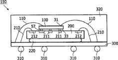
图2示出了电子器件150的第一实施例。在此实施例中,第一芯片100和第二芯片200的组件与载体300结合成一种封装。用焊球57将第一芯片100和第二芯片200相互电气耦接,这些焊球57位于第一芯片100中的这些第一侧面接触衬垫33与对应的第二芯片200中的接触衬垫211之间。用第二芯片200的底侧通过模片附着层220将第二芯片200附接到载体300。适当地用未充满材料将第一芯片100与第二芯片200之间的空间填充,但在图中未示出。第一芯片100中的这些第二侧面接触衬垫31处于第二侧面。引线接合110形成这些第二侧面接触衬垫31与载体300上的导电引线之间的连接。这种载体通常是一种本领域中熟练的技术人员公知的叠层或引线框。第二芯片200包括邻近于在第一芯片100下面的接触衬垫211的另外的接触衬垫212。在此示例中,将这些接触衬垫适当地设在第二芯片200的外围,以使这些接触衬垫并不在第二芯片200中的任何主动元件的上面,图2中并未示出这些主动元件。这些另外的接触衬垫212适当地具有较大的直径和经过补强的底层结构,以使这些接触衬垫212适用于引线接合。在这些另外的接触衬垫212与载体300上的导电引线之间设有线210。模320设在该载体上,以封装第一芯片100、第二芯片200和接合线110、210。将焊球310设在该载体的底侧上,以置于外部元器件上,尤其是印刷电路板上。FIG. 2 shows a first embodiment of an
图3示出了电子器件150的第二实施例,该实施例同样也包括第一芯片100、第二芯片200和外部载体300。在此实施例中,第一芯片100和第二芯片200具有相同的侧向延伸。这就在已将带有第一芯片100的晶片和带有第二芯片200的晶片组装在一起之后可进行分离的意义上便于组装。已利用蚀刻技术在这两种晶片制备了分离通道。在将这些分离通道暂时填充之后,可利用任何适当的分离技术将这些组件单个化(singulate),适当的技术包括蚀刻和锯切。FIG. 3 shows a second exemplary embodiment of an
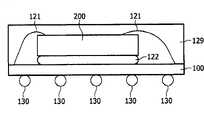
图4示出了组件140的另一个实施例。在此示例中无另外的载体出现。组件140设计用作芯片级封装。对这些焊球130进行选择以适于直接置于印刷电路板上。图中示出的未充满材料219位于第一芯片100与第二芯片200之间并封装焊球连接。正如将会理解的那样,第一芯片100和第二芯片200配合是特别适当的,因为与焊球57的数量相比,这样可减少焊球130的数量。因此,焊球130之间的间距可非常大,且焊球130的高度也可非常大。通常用在这些芯片级封装中的高度是最佳的。Another embodiment of
图5示出了这种组件140的第二实施例。在此实施例中,第一芯片100具有小于第二芯片200的侧向延伸。焊球230设在该第二芯片的另外的接触衬垫212上。为了使这种组件发挥作用,这些焊球230的高度需等于第一芯片100与第二芯片200之间的焊球130、第一芯片100和焊球57的高度。因此,使用小尺寸的焊球57优选焊帽以及非常薄的第一芯片100是适当的。此外,可通过另外的金属喷镀级或较厚的下凸块金属喷镀使接触衬垫212向上。FIG. 5 shows a second embodiment of such an
图6示出了这种组件140的第三实施例,该实施例类似于图5中的实施例。在此实施例中,第一芯片100侧向延伸并超过第二芯片200。因此,第一芯片100就适于作为常规的芯片载体。封装129确保将组件密封以防水汽和防尘。FIG. 6 shows a third embodiment of such an
图7示出了这种组件140的第四实施例,该实施例是第三实施例的延伸。在此情形中,第一芯片100起到用于第二芯片200的另一种芯片250的载体的作用,用焊球257将该另一种芯片250耦接到该第一芯片。在此实施例中,将这些焊球57、257设在第一芯片100上是适当的,但并不是必需的。FIG. 7 shows a fourth embodiment of such an
图8示出了这种组件140的第五实施例,在此实施例中,用模片附件122将第二芯片200附接到第一芯片100。然后将第一芯片100弯曲,这样就在第二芯片200的相对侧面构成到这些焊球57的互连。用任何封装材料将第一芯片100与第二芯片200之间的任何空间填充。现已观察到这种组件概念150也可有其它变体,尤其是在希望第二芯片200包括与印刷电路板成大于0°的角的用途中。因此,在将第一芯片100弯曲之前将第二芯片200组装到第一芯片100。在另一个步骤中,以所希望的角度将该第一芯片弯曲,以重新定向第二芯片200。最后提供巩固第二芯片200的重新定向的模塑材料。因此,用于外部连接的接触衬垫处于并未弯曲的区域内,但这并不是必需的。FIG. 8 shows a fifth embodiment of such an
图9公开了这种组件140的第六实施例。在此实施例中,第一芯片与第二芯片200之间的电气连接由引线接合121构成。这种组件140的优点在于这种组件非常类似于常规的球门阵列封装,而仍包括第一芯片100和第二芯片200。FIG. 9 discloses a sixth embodiment of such an
简而言之,一种第一芯片100和第二芯片200的组件,这种组件的第一芯片100具有柔性并在芯片100的相对侧面1,2上设有第一树脂层12和第二树脂层52,这种组件允许将第一芯片保持在压缩状态,第一侧面接触衬垫33和第二侧面接触衬垫31分别处于第一侧面1和第二侧面2上,这些第一侧面接触衬垫33耦接到对应的第二芯片200的接触衬垫211,且这些第二侧面接触衬垫31设计用于这种组件的外部连接。In short, an assembly of a
Claims (14)
Translated fromChineseApplications Claiming Priority (2)
| Application Number | Priority Date | Filing Date | Title |
|---|---|---|---|
| EP05110653 | 2005-11-11 | ||
| EP05110653.2 | 2005-11-11 |
Publications (2)
| Publication Number | Publication Date |
|---|---|
| CN101305464Atrue CN101305464A (en) | 2008-11-12 |
| CN100592513C CN100592513C (en) | 2010-02-24 |
Family
ID=37770339
Family Applications (1)
| Application Number | Title | Priority Date | Filing Date |
|---|---|---|---|
| CN200680041943AExpired - Fee RelatedCN100592513C (en) | 2005-11-11 | 2006-11-07 | Chip component and method for manufacturing chip component |
Country Status (6)
| Country | Link |
|---|---|
| US (1) | US20080290511A1 (en) |
| EP (1) | EP1949441A2 (en) |
| JP (1) | JP2009516369A (en) |
| CN (1) | CN100592513C (en) |
| TW (1) | TW200731490A (en) |
| WO (1) | WO2007054894A2 (en) |
Families Citing this family (9)
| Publication number | Priority date | Publication date | Assignee | Title |
|---|---|---|---|---|
| TWI423414B (en)* | 2009-02-20 | 2014-01-11 | Nat Semiconductor Corp | Integrated circuit micro-module |
| JP2013206942A (en)* | 2012-03-27 | 2013-10-07 | Sharp Corp | Semiconductor device |
| DE102014018277A1 (en)* | 2014-12-12 | 2016-06-16 | Tesat-Spacecom Gmbh & Co. Kg | Method for providing high voltage insulation of electrical components |
| TWI605557B (en)* | 2015-12-31 | 2017-11-11 | 矽品精密工業股份有限公司 | Electronic package, method for fabricating the electronic package, and substrate structure |
| DE102016103585B4 (en)* | 2016-02-29 | 2022-01-13 | Infineon Technologies Ag | Process for manufacturing a package with solderable electrical contact |
| CN105789163A (en)* | 2016-03-23 | 2016-07-20 | 宜确半导体(苏州)有限公司 | Radio frequency front-end chip integration module and radio frequency front-end chip integration method |
| CN111480230B (en)* | 2017-12-22 | 2024-06-21 | Hrl实验有限公司 | Hybrid integrated circuit structure |
| CN109545757A (en)* | 2018-11-20 | 2019-03-29 | 苏州晶方半导体科技股份有限公司 | The encapsulating structure and packaging method of chip |
| US11545404B2 (en)* | 2020-05-06 | 2023-01-03 | Qualcomm Incorporated | III-V compound semiconductor dies with stress-treated inactive surfaces to avoid packaging-induced fractures, and related methods |
Family Cites Families (11)
| Publication number | Priority date | Publication date | Assignee | Title |
|---|---|---|---|---|
| US6027958A (en)* | 1996-07-11 | 2000-02-22 | Kopin Corporation | Transferred flexible integrated circuit |
| EP0913268A4 (en)* | 1997-05-19 | 2004-11-17 | Hitachi Maxell | FLEXIBLE INTEGRATED CIRCUIT MODULE AND ITS PRODUCTION METHOD, INFORMATION MEDIUM PRODUCTION METHOD COMPRISING SAID MODULE |
| EP1041624A1 (en)* | 1999-04-02 | 2000-10-04 | Interuniversitair Microelektronica Centrum Vzw | Method of transferring ultra-thin substrates and application of the method to the manufacture of a multilayer thin film device |
| KR100533673B1 (en)* | 1999-09-03 | 2005-12-05 | 세이코 엡슨 가부시키가이샤 | Semiconductor device, method of manufacture thereof, circuit board, and electronic device |
| JP4100936B2 (en)* | 2002-03-01 | 2008-06-11 | Necエレクトロニクス株式会社 | Manufacturing method of semiconductor device |
| US6798057B2 (en)* | 2002-11-05 | 2004-09-28 | Micron Technology, Inc. | Thin stacked ball-grid array package |
| JP3740469B2 (en)* | 2003-01-31 | 2006-02-01 | 株式会社東芝 | Semiconductor device and manufacturing method of semiconductor device |
| DE10320646A1 (en)* | 2003-05-07 | 2004-09-16 | Infineon Technologies Ag | Electronic component, typically integrated circuit, system support and manufacturing method, with support containing component positions in lines and columns, starting with coating auxiliary support with photosensitive layer |
| TWI278048B (en)* | 2003-11-10 | 2007-04-01 | Casio Computer Co Ltd | Semiconductor device and its manufacturing method |
| JP4298559B2 (en)* | 2004-03-29 | 2009-07-22 | 新光電気工業株式会社 | Electronic component mounting structure and manufacturing method thereof |
| ATE412251T1 (en)* | 2005-03-02 | 2008-11-15 | Koninkl Philips Electronics Nv | PRODUCTION PROCESS FOR SEMICONDUCTOR HOUSINGS AND HOUSINGS PRODUCED BY THIS METHOD |
- 2006
- 2006-11-07CNCN200680041943Apatent/CN100592513C/ennot_activeExpired - Fee Related
- 2006-11-07USUS12/093,336patent/US20080290511A1/ennot_activeAbandoned
- 2006-11-07JPJP2008539580Apatent/JP2009516369A/ennot_activeWithdrawn
- 2006-11-07WOPCT/IB2006/054149patent/WO2007054894A2/enactiveApplication Filing
- 2006-11-07EPEP06821360Apatent/EP1949441A2/ennot_activeWithdrawn
- 2006-11-08TWTW095141428Apatent/TW200731490A/enunknown
Also Published As
| Publication number | Publication date |
|---|---|
| JP2009516369A (en) | 2009-04-16 |
| WO2007054894A3 (en) | 2007-11-15 |
| EP1949441A2 (en) | 2008-07-30 |
| WO2007054894A2 (en) | 2007-05-18 |
| US20080290511A1 (en) | 2008-11-27 |
| CN100592513C (en) | 2010-02-24 |
| TW200731490A (en) | 2007-08-16 |
Similar Documents
| Publication | Publication Date | Title |
|---|---|---|
| US11270965B2 (en) | Semiconductor device with thin redistribution layers | |
| CN107768351B (en) | Semiconductor package with thermo-electromechanical chip and method of forming the same | |
| US7326592B2 (en) | Stacked die package | |
| CN106505045B (en) | Semiconductor package and method with routable encapsulated conductive substrate | |
| US9418970B2 (en) | Redistribution layers for microfeature workpieces, and associated systems and methods | |
| US7364944B2 (en) | Method for fabricating thermally enhanced semiconductor package | |
| CN100592513C (en) | Chip component and method for manufacturing chip component | |
| EP3093877B1 (en) | Semiconductor package | |
| EP1471571B1 (en) | Semiconductor device and manufacturing method thereof | |
| US7242081B1 (en) | Stacked package structure | |
| US20100164079A1 (en) | Method of manufacturing an assembly and assembly | |
| US20110209908A1 (en) | Conductor package structure and method of the same | |
| CN101211945A (en) | Semiconductor image element packaging structure with crystal grain receiving through hole and method thereof | |
| US20090267219A1 (en) | Ultra-thin chip packaging | |
| CN113471188A (en) | Semiconductor package and method of manufacturing the same | |
| JP2008258604A (en) | Semiconductor device package having multi-chip in parallel configuration and manufacturing method thereof | |
| TWI622153B (en) | System-in-package and method for fabricating the same | |
| US20120326300A1 (en) | Low profile package and method | |
| KR100890073B1 (en) | Vertically Stacked Semiconductor Devices and Manufacturing Method Thereof | |
| CN112310065A (en) | Package structure, assembly structure and manufacturing method thereof | |
| US20110031607A1 (en) | Conductor package structure and method of the same | |
| KR100666919B1 (en) | Adhesive sheet for semiconductor package, semiconductor device comprising same, multi-stack package comprising same, method for manufacturing semiconductor device and method for manufacturing multi-stack package | |
| US9082738B2 (en) | Semiconductor package with improved thermal properties | |
| US20050082658A1 (en) | Simplified stacked chip assemblies | |
| US20040207065A1 (en) | [stack-type multi-chip package and method of fabricating bumps on the backside of a chip] |
Legal Events
| Date | Code | Title | Description |
|---|---|---|---|
| C06 | Publication | ||
| PB01 | Publication | ||
| C10 | Entry into substantive examination | ||
| SE01 | Entry into force of request for substantive examination | ||
| C14 | Grant of patent or utility model | ||
| GR01 | Patent grant | ||
| C17 | Cessation of patent right | ||
| CF01 | Termination of patent right due to non-payment of annual fee | Granted publication date:20100224 Termination date:20101107 |