CN101303897A - Memory, repair system and test method thereof - Google Patents
Memory, repair system and test method thereofDownload PDFInfo
- Publication number
- CN101303897A CN101303897ACNA2007101490084ACN200710149008ACN101303897ACN 101303897 ACN101303897 ACN 101303897ACN A2007101490084 ACNA2007101490084 ACN A2007101490084ACN 200710149008 ACN200710149008 ACN 200710149008ACN 101303897 ACN101303897 ACN 101303897A
- Authority
- CN
- China
- Prior art keywords
- memory
- storage unit
- test
- data
- unit
- Prior art date
- Legal status (The legal status is an assumption and is not a legal conclusion. Google has not performed a legal analysis and makes no representation as to the accuracy of the status listed.)
- Pending
Links
Images

Classifications
- G—PHYSICS
- G11—INFORMATION STORAGE
- G11C—STATIC STORES
- G11C29/00—Checking stores for correct operation ; Subsequent repair; Testing stores during standby or offline operation
- G11C29/04—Detection or location of defective memory elements, e.g. cell constructio details, timing of test signals
- G11C29/08—Functional testing, e.g. testing during refresh, power-on self testing [POST] or distributed testing
- G11C29/12—Built-in arrangements for testing, e.g. built-in self testing [BIST] or interconnection details
- G11C29/38—Response verification devices
- G11C29/42—Response verification devices using error correcting codes [ECC] or parity check
- G—PHYSICS
- G06—COMPUTING OR CALCULATING; COUNTING
- G06F—ELECTRIC DIGITAL DATA PROCESSING
- G06F11/00—Error detection; Error correction; Monitoring
- G06F11/07—Responding to the occurrence of a fault, e.g. fault tolerance
- G06F11/08—Error detection or correction by redundancy in data representation, e.g. by using checking codes
- G06F11/10—Adding special bits or symbols to the coded information, e.g. parity check, casting out 9's or 11's
- G06F11/1008—Adding special bits or symbols to the coded information, e.g. parity check, casting out 9's or 11's in individual solid state devices
- G—PHYSICS
- G11—INFORMATION STORAGE
- G11C—STATIC STORES
- G11C29/00—Checking stores for correct operation ; Subsequent repair; Testing stores during standby or offline operation
- G11C29/04—Detection or location of defective memory elements, e.g. cell constructio details, timing of test signals
- G11C29/08—Functional testing, e.g. testing during refresh, power-on self testing [POST] or distributed testing
- G11C29/12—Built-in arrangements for testing, e.g. built-in self testing [BIST] or interconnection details
- G11C29/44—Indication or identification of errors, e.g. for repair
- G—PHYSICS
- G11—INFORMATION STORAGE
- G11C—STATIC STORES
- G11C29/00—Checking stores for correct operation ; Subsequent repair; Testing stores during standby or offline operation
- G11C29/04—Detection or location of defective memory elements, e.g. cell constructio details, timing of test signals
- G11C2029/0411—Online error correction
- G—PHYSICS
- G11—INFORMATION STORAGE
- G11C—STATIC STORES
- G11C29/00—Checking stores for correct operation ; Subsequent repair; Testing stores during standby or offline operation
- G11C29/04—Detection or location of defective memory elements, e.g. cell constructio details, timing of test signals
- G11C29/08—Functional testing, e.g. testing during refresh, power-on self testing [POST] or distributed testing
- G11C29/12—Built-in arrangements for testing, e.g. built-in self testing [BIST] or interconnection details
- G11C2029/1208—Error catch memory
Landscapes
- Engineering & Computer Science (AREA)
- Theoretical Computer Science (AREA)
- Quality & Reliability (AREA)
- Physics & Mathematics (AREA)
- General Engineering & Computer Science (AREA)
- General Physics & Mathematics (AREA)
- For Increasing The Reliability Of Semiconductor Memories (AREA)
- Techniques For Improving Reliability Of Storages (AREA)
- Detection And Correction Of Errors (AREA)
Abstract
Description
Translated fromChinese技术领域technical field
本发明有关于一种存储器,且特别是有关于一种可用来改善合格率并可可快速测试的存储器。The present invention relates to a memory, and more particularly to a memory that can be used to improve yield and allow rapid testing.
背景技术Background technique
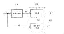
存储器的制造包括一测试存于存储器内的数据的步骤。图1表示一存储器阵列110与用以测试存储器阵列110的一测试器120。测试器120包括一比较器121与一数据缓冲存储器122。一原始数据D0(未表示)被写入至存储器阵列120中的每个待测试的存储单元。数据缓冲存储器122亦存储一参考数据D2,其为原始数据D0的正确复制数据。当一输入地址AI提供给存储器阵列110与数据缓冲存储器122时,由对应输入地址AI的存储单元所读取到的测试数据D1与数据缓冲存储器122中的对应参考数据D2被分别被输入至比较器121。比较器121将对应参考数据D2与测试数据D1进行比较,并输出一输出信号So,以指出原始数据D0是否被正确地存储于对应输入地址AI的存储单元中,以决定存储单元为正确与否。The manufacture of memory includes a step of testing the data stored in the memory. FIG. 1 shows a
然而,随着存储器阵列的存储容量越来越大,以传统测试器一个一个测试存储器阵列中的存储单元会变得十分耗时。此外,数据缓冲存储器122的存储容量亦需大幅增加。因此,如何提供一个可较有效率地被测试的存储器,乃本领域所致力的目标。However, as the storage capacity of the memory array increases, it becomes very time-consuming to test the memory cells in the memory array one by one with a traditional tester. In addition, the storage capacity of the
发明内容Contents of the invention
本发明有关于一种存储器。在测试该存储器的存储单元期间,只要该存储器的错误校正码单元能够正确地校正由存储单元读取出来的测试数据中的错误,该存储单元即可被判定为测试通过。因此,应用该存储器可以有效改善合格率。The present invention relates to a memory. During the test of the storage unit of the memory, as long as the error correction code unit of the memory can correctly correct the errors in the test data read from the storage unit, the storage unit can be judged to pass the test. Therefore, the application of this memory can effectively improve the yield.
根据本发明的第一方面,提出一种存储器。该存储器包括一存储器阵列、一错误校正码(Error correct code,ECC)单元与一比较器。存储器阵列包括至少一存储单元。该存储单元被写入并存储至少一原始数据。错误校正码单元用以从存储单元读取出至少一测试数据。若该测试数据出现一错误,则错误校正码单元即校正该测试数据。错误校正码单元并据以输出一错误校正数据。比较器用以判定原始数据是否与错误校正数据相同,并输出一输出信号来指示存储单元为测试成功与否。According to a first aspect of the present invention, a memory is proposed. The memory includes a memory array, an error correct code (ECC) unit and a comparator. The memory array includes at least one memory unit. The storage unit is written and stores at least one original data. The ECC unit is used for reading at least one test data from the storage unit. If an error occurs in the test data, the error correction code unit corrects the test data. The error correction code unit outputs an error correction data accordingly. The comparator is used to determine whether the original data is the same as the error correction data, and outputs an output signal to indicate whether the memory unit is tested successfully or not.
根据本发明的第二方面,提出一种测试方法,用以测试一存储器的至少一存储单元。该方法包括:首先,将至少一原始数据写入至存储单元中。的后,由存储单元读取出至少一测试数据,并对该测试数据执行错误校正码运算,并据以输出至少一错误校正数据。接着,决定错误校正数据是否与原始数据相等,以决定存储单元为测试成功与否。According to a second aspect of the present invention, a testing method is provided for testing at least one storage unit of a memory. The method includes: first, writing at least one original data into the storage unit. After that, at least one test data is read out from the storage unit, and an error correction code operation is performed on the test data, and at least one error correction data is output accordingly. Then, it is determined whether the error correction data is equal to the original data, so as to determine whether the test of the memory unit is successful or not.
为让本发明的上述内容能更明显易懂,下文特举一较佳实施例,并配合附图,详细说明如下:In order to make the above-mentioned content of the present invention more obvious and understandable, a preferred embodiment is given below, together with the accompanying drawings, and the detailed description is as follows:
附图说明Description of drawings
图1表示一存储器阵列与用以测试存储器阵列的一测试器。FIG. 1 shows a memory array and a tester for testing the memory array.
图2表示依据本发明实施例的存储器的方块图。FIG. 2 shows a block diagram of a memory according to an embodiment of the invention.
图3表示并行测试数个具有图2的存储器的存储器的方块图。FIG. 3 shows a block diagram for testing several memories having the memory of FIG. 2 in parallel.
图4表示依照本发明实施例的测试方法,用以测试图2的存储器。FIG. 4 shows a testing method for testing the memory in FIG. 2 according to an embodiment of the present invention.
主要元件符号说明Description of main component symbols
110、210:存储器阵列110, 210: memory array
120、310:测试器120, 310: tester
121、230:比较器121, 230: Comparator
122:数据缓冲存储器122: Data buffer memory
211~21N:存储单元211~21N: storage unit
220:错误校正码单元220: error correction code unit
240:错误记录单元240: error logging unit
321~32M:存储器321~32M: memory
具体实施方式Detailed ways
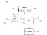
图2表示依据本发明实施例的存储器的方块图。请参考图2。存储器200包括一存储器阵列210、一错误校正码(Error correct code,ECC)单元220与一比较器230。FIG. 2 shows a block diagram of a memory according to an embodiment of the invention. Please refer to Figure 2. The
存储器阵列210包括存储单元211至21N。N为一正整数。一原始数据Dg(未表示)依据输入地址Ad被写入至每个存储单元。其中,存于存储单元211至21N的数据被定义为测试数据Dt。错误校正码单元220用以读取测试数据Dt,并执行一错误校正码运算。当一错误出现于测试数据Dt,错误校正码单元220执行错误校正码运算来校正测试数据Dt,并据以输出一错误校正数据De。The
比较器230比较错误校正数据De与原始数据Dg,并输出一输出信号So来指示错误校正数据De否与原始数据Dg相同。如此一来,即可判断存储单元211至21N是否可以正确地被存取原始数据Dg,以决定存储单元211至21N正确与否。The
若错误校正数据De与原始数据Dg相同,表示由存储单元211至21N所读取出的测试数据Dt即为正确,或表示若有错误出现于测试数据Dt时,错误校正码单元220可以正确地校正测试数据Dt。比较器230即输出输出信号So,以表示存储单元211至21N为测试正确。亦即,只要错误校正码单元220可以成功地校正由存储单元211至21N所读取出的测试数据Dt中的错误,存储单元211至21N即被判定为测试正确。If the error correction data De is identical to the original data Dg, it means that the test data Dt read by the
若错误校正数据De未与原始数据Dg相同,表示测试数据Dt无法正确地由存储单元被读取出来,且无法由错误校正码单元220成功地校正。因此,比较器230输出输出信号So来指示存储单元211至21N为测试错误。亦即,当测试数据Dt中有错误出现,且即使错误校正码单元220亦无法成功地校正测试数据Dt时,存储单元211至21N即被判定为测试失败。If the error correction data De is not the same as the original data Dg, it means that the test data Dt cannot be correctly read from the storage unit, and cannot be successfully corrected by the error
举例来说,当错误校正码单元220用以执行一位的错误校正码运算(1-bit ECC operation)时,在测试数据Dt中的一位的错误可以被成功地校正。亦即,对于存储单元211至21N,一位的错误是可容忍的。因此,即使测试数据De中出现一位的错误,存储单元211至21N仍可被判定为测试通过。然而,当超过一位的错误出现于测试数据Dt中,使用一位的错误校正码单元220即无法正确地校正。因此,存储单元211至21N即被判定为测试失败。使用一位的错误校正码单元,编程的合格率与编程速度可以增加5%至10%。For example, when the
存储器200还包括一错误记录单元240。在本发明实施例中,错误记录单元240记录错误存储单元的地址。另一个正确的存储单元用来取代该错误的存储单元。如此,当欲存取该已记录的存储单元时,即会存取到用以取代的正确存储单元。The
在本发明实施例中,存储单元211至21N位于存储器阵列210中的一存储行或一存储列中。当错误校正数据De未与原始数据Dg相等时,亦即,当太多位的错误出现于一存储列中,且无法以错误校正码运算来校正并复原时,该存储列的地址可以被纪录为测试失败,并记录于错误记录单元240中。存储器阵列210可以被实现为一修复系统。存储器阵列210中的一修复行可被用来取代该存储列。另一原始数据被写入至该修复行中,以决定该修复行正确与否。当使用存储器时,若该错误的存储列被存取到,即会重新指向该修复行,以存取该修复行。In the embodiment of the present invention, the
同样地,当位于存储器阵列210中的一存储列被判定为测试失败,存储列的地址亦被纪录为测试失败,并记录于错误记录单元240中。存储器阵列210中的一修复列可被用来取代该存储列。另一原始数据被写入至该修复列中,以决定该修复列正确与否。当使用存储器时,若该错误的存储列被存取到,即会重新指向该修复列,以存取该修复列。Similarly, when a memory bank in the
在本发明实施例中,藉由存储等于0与1的原始数据Dg,来测试每个存储单元211至21N,以验证其是否可正确地存取0与1。In the embodiment of the present invention, by storing the original data Dg equal to 0 and 1, each
原始数据Dg被一测试器写入至存储器阵列中。该测试器亦接收输出信号So,以判定所测试的存储单元为测试成功或测试失败。The raw data Dg is written into the memory array by a tester. The tester also receives the output signal So to determine whether the tested memory unit is tested successfully or failed.
图3表示并行测试具有存储器200的存储器321至32M的方块图。其中,M为一正整数。测试器310分别输入原始数据Dg1至DgM至存储器321至32M,以测试其存储器阵列。其存储器阵列的存储单元以前述方式来测试。用以指示存储器321至32M的存储器阵列的存储单元正确与否的输出信号So1至SoM,分别被输出至测试器310。FIG. 3 shows a block diagram for testing the memories 321 to 32M with the
在测试存储器时,仅需要测试器310的一测试接脚来接收每个存储器的输出信号。如此,测试器310即可同时测试更多的存储器。相较之下,具有传统存储器的存储器的测试方式,为一个一个测试每个存储单元。测试器310的一个测试接脚仅能用以接收对应单一存储单元的输出信号。因此,测试一个具有传统存储器的存储器需使用更多测试接脚。因此,测试器310可以并行地测试更多具有本发明实施例的存储器的存储器,以加速生产流程。When testing the memory, only one test pin of the
图4表示依照本发明实施例的测试方法,用以测试存储器200。首先,在步骤410中,写入原始数据Dg至存储单元211至21N。接着,在步骤420中,由存储单元211至21N读取测试数据Dt,并对测试数据Dt执行错误校正运算,并据以输出一错误校正数据De。FIG. 4 shows a testing method for testing the
之后,在步骤430中,决定错误校正数据De是否与原始数据Dg相同,以判定存储单元211至21N为测试成功或测试失败。接着,在步骤440中,当存储单元211至21N被判定为错误失败时,记录错误的存储单元211至21N的地址。Afterwards, in step 430 , it is determined whether the error correction data De is the same as the original data Dg, so as to determine whether the test of the
在测试本发明实施例的存储器的存储单元时,只要其错误校正单元可以成功地校正由存储单元所读取出的测试数据的错误,该存储单元即被判定为测试成功。因此,使用该存储器可以改善合格率。When testing the storage unit of the memory according to the embodiment of the present invention, as long as its error correction unit can successfully correct the error of the test data read from the storage unit, the storage unit is determined to be tested successfully. Therefore, using this memory can improve the yield.
此外,具有该存储器的存储器,仅需测试器中的一个测试接脚,来接收指示存储器的存储单元为正确与否的输出信号。因此,测试器可以并行地测试更多具有该存储器的存储器。如此,藉由应用本发明实施例的存储器,可以显著提升存储器的测试速度,而改善制造效率。In addition, the memory with the memory only needs one test pin in the tester to receive the output signal indicating whether the storage unit of the memory is correct or not. Therefore, the tester can test more memories with that memory in parallel. In this way, by applying the memory of the embodiment of the present invention, the test speed of the memory can be significantly increased, and the manufacturing efficiency can be improved.
虽然本发明已以较佳实施例公开如上,然其并非用以限定本发明。任何所属技术领域中的普通技术人员,在不脱离本发明的精神和范围的情况下,可进行各种更动与修改。因此,本发明的保护范围以所提出的权利要求的范围为准。Although the present invention has been disclosed above with preferred embodiments, it is not intended to limit the present invention. Various changes and modifications can be made by those skilled in the art without departing from the spirit and scope of the present invention. Accordingly, the protection scope of the present invention shall be determined by the scope of the appended claims.
Claims (10)
Applications Claiming Priority (2)
| Application Number | Priority Date | Filing Date | Title |
|---|---|---|---|
| US11/798,292 | 2007-05-11 | ||
| US11/798,292US20080282120A1 (en) | 2007-05-11 | 2007-05-11 | Memory structure, repair system and method for testing the same |
Related Child Applications (1)
| Application Number | Title | Priority Date | Filing Date |
|---|---|---|---|
| CN2013100621731ADivisionCN103177770A (en) | 2007-05-11 | 2007-09-04 | Memory, repair system and testing method thereof |
Publications (1)
| Publication Number | Publication Date |
|---|---|
| CN101303897Atrue CN101303897A (en) | 2008-11-12 |
Family
ID=39970642
Family Applications (2)
| Application Number | Title | Priority Date | Filing Date |
|---|---|---|---|
| CN2013100621731APendingCN103177770A (en) | 2007-05-11 | 2007-09-04 | Memory, repair system and testing method thereof |
| CNA2007101490084APendingCN101303897A (en) | 2007-05-11 | 2007-09-04 | Memory, repair system and test method thereof |
Family Applications Before (1)
| Application Number | Title | Priority Date | Filing Date |
|---|---|---|---|
| CN2013100621731APendingCN103177770A (en) | 2007-05-11 | 2007-09-04 | Memory, repair system and testing method thereof |
Country Status (3)
| Country | Link |
|---|---|
| US (1) | US20080282120A1 (en) |
| CN (2) | CN103177770A (en) |
| TW (1) | TWI359424B (en) |
Cited By (5)
| Publication number | Priority date | Publication date | Assignee | Title |
|---|---|---|---|---|
| CN102402961A (en)* | 2011-11-09 | 2012-04-04 | 友达光电股份有限公司 | Self-test driving circuit |
| CN105719702A (en)* | 2016-01-26 | 2016-06-29 | 中国科学院微电子研究所 | Improved memory error detection method and device |
| CN106024062A (en)* | 2016-07-19 | 2016-10-12 | 北京兆易创新科技股份有限公司 | Data reading device and method of nonvolatile memory |
| CN106933696A (en)* | 2015-12-31 | 2017-07-07 | 北京国睿中数科技股份有限公司 | ECC function verification methods |
| CN114416441A (en)* | 2021-12-06 | 2022-04-29 | 浙江中控技术股份有限公司 | Real-time database automatic testing method and system, electronic equipment and storage medium |
Families Citing this family (6)
| Publication number | Priority date | Publication date | Assignee | Title |
|---|---|---|---|---|
| US8270222B2 (en)* | 2009-09-24 | 2012-09-18 | Macronix International Co., Ltd. | Local word line driver of a memory |
| US9223665B2 (en) | 2013-03-15 | 2015-12-29 | Micron Technology, Inc. | Apparatuses and methods for memory testing and repair |
| US9911509B2 (en)* | 2013-12-06 | 2018-03-06 | Intel Corporation | Counter to locate faulty die in a distributed codeword storage system |
| US20160054382A1 (en)* | 2014-08-22 | 2016-02-25 | Nanya Technology Corporation | Method for checking result of chip probing test and chip thereof |
| CN108572887A (en)* | 2017-03-14 | 2018-09-25 | 上海骐宏电驱动科技有限公司 | Data detection bearing calibration |
| US10679718B2 (en)* | 2017-10-04 | 2020-06-09 | Western Digital Technologies, Inc. | Error reducing matrix generation |
Family Cites Families (14)
| Publication number | Priority date | Publication date | Assignee | Title |
|---|---|---|---|---|
| US3434116A (en)* | 1966-06-15 | 1969-03-18 | Ibm | Scheme for circumventing bad memory cells |
| JPS57150197A (en)* | 1981-03-11 | 1982-09-16 | Nippon Telegr & Teleph Corp <Ntt> | Storage circuit |
| US5313624A (en)* | 1991-05-14 | 1994-05-17 | Next Computer, Inc. | DRAM multiplexer |
| US6026505A (en)* | 1991-10-16 | 2000-02-15 | International Business Machines Corporation | Method and apparatus for real time two dimensional redundancy allocation |
| US5379415A (en)* | 1992-09-29 | 1995-01-03 | Zitel Corporation | Fault tolerant memory system |
| US5675545A (en)* | 1995-09-08 | 1997-10-07 | Ambit Design Systems, Inc. | Method of forming a database that defines an integrated circuit memory with built in test circuitry |
| US5600658A (en)* | 1995-10-19 | 1997-02-04 | National Semiconductor Corporation | Built-in self tests for large multiplier, adder, or subtractor |
| US5995731A (en)* | 1997-12-29 | 1999-11-30 | Motorola, Inc. | Multiple BIST controllers for testing multiple embedded memory arrays |
| FR2790832B1 (en)* | 1999-03-08 | 2001-06-08 | France Telecom | INTEGRATED CIRCUIT TEST PROCESS WITH ACCESS TO CIRCUIT MEMORIZATION POINTS |
| US6587979B1 (en)* | 1999-10-18 | 2003-07-01 | Credence Systems Corporation | Partitionable embedded circuit test system for integrated circuit |
| JP3914839B2 (en)* | 2002-07-11 | 2007-05-16 | エルピーダメモリ株式会社 | Semiconductor memory device |
| JP2007257791A (en)* | 2006-03-24 | 2007-10-04 | Fujitsu Ltd | Semiconductor memory device |
| US7802157B2 (en)* | 2006-06-22 | 2010-09-21 | Micron Technology, Inc. | Test mode for multi-chip integrated circuit packages |
| US7549098B2 (en)* | 2006-12-19 | 2009-06-16 | International Business Machines Corporation | Redundancy programming for a memory device |
- 2007
- 2007-05-11USUS11/798,292patent/US20080282120A1/ennot_activeAbandoned
- 2007-08-24TWTW096131587Apatent/TWI359424B/enactive
- 2007-09-04CNCN2013100621731Apatent/CN103177770A/enactivePending
- 2007-09-04CNCNA2007101490084Apatent/CN101303897A/enactivePending
Cited By (7)
| Publication number | Priority date | Publication date | Assignee | Title |
|---|---|---|---|---|
| CN102402961A (en)* | 2011-11-09 | 2012-04-04 | 友达光电股份有限公司 | Self-test driving circuit |
| CN102402961B (en)* | 2011-11-09 | 2014-06-25 | 友达光电股份有限公司 | Self-test driving circuit |
| CN106933696A (en)* | 2015-12-31 | 2017-07-07 | 北京国睿中数科技股份有限公司 | ECC function verification methods |
| CN105719702A (en)* | 2016-01-26 | 2016-06-29 | 中国科学院微电子研究所 | Improved memory error detection method and device |
| CN106024062A (en)* | 2016-07-19 | 2016-10-12 | 北京兆易创新科技股份有限公司 | Data reading device and method of nonvolatile memory |
| CN106024062B (en)* | 2016-07-19 | 2023-12-05 | 兆易创新科技集团股份有限公司 | Data reading device and method of nonvolatile memory |
| CN114416441A (en)* | 2021-12-06 | 2022-04-29 | 浙江中控技术股份有限公司 | Real-time database automatic testing method and system, electronic equipment and storage medium |
Also Published As
| Publication number | Publication date |
|---|---|
| TW200845020A (en) | 2008-11-16 |
| TWI359424B (en) | 2012-03-01 |
| US20080282120A1 (en) | 2008-11-13 |
| CN103177770A (en) | 2013-06-26 |
Similar Documents
| Publication | Publication Date | Title |
|---|---|---|
| CN101303897A (en) | Memory, repair system and test method thereof | |
| US8327224B2 (en) | Data recovery in a solid state storage system | |
| US8799717B2 (en) | Hardwired remapped memory | |
| TWI438776B (en) | Method and apparatus for repairing high capacity/high bandwidth memory devices | |
| CN108877870B (en) | Repair circuit for repair operation and memory device including repair circuit | |
| CN101763904B (en) | Nonvolatile memory devices and operational approach thereof | |
| CN110289041A (en) | A memory detection device combining BIST and ECC in a system chip | |
| US9396815B2 (en) | Memory structure | |
| US9514843B2 (en) | Methods for accessing a storage unit of a flash memory and apparatuses using the same | |
| US4251863A (en) | Apparatus for correction of memory errors | |
| CN102479554A (en) | Device and method for repair analysis | |
| CN113393889A (en) | Memory system | |
| JP2005332436A (en) | Semiconductor device and test method thereof | |
| US10353769B2 (en) | Recovering from addressing fault in a non-volatile memory | |
| US10043588B2 (en) | Memory device | |
| US9183952B2 (en) | Apparatuses and methods for compressing data received over multiple memory accesses | |
| KR20110010381A (en) | Semiconductor memory device including self repair function and its self repair method | |
| CN113345511A (en) | Memory device and test method thereof | |
| CN110289040A (en) | A memory detection method combining BIST and ECC in a system chip | |
| CN109215724B (en) | Method and device for automatically detecting and repairing memory | |
| US11574699B2 (en) | Semiconductor device equipped with global column redundancy | |
| CN110827878A (en) | Memory device | |
| WO2021196621A1 (en) | Read/write method and memory apparatus | |
| WO2021196619A1 (en) | Reading and writing method and memory apparatus | |
| WO2021196623A1 (en) | Read-write method and memory device |
Legal Events
| Date | Code | Title | Description |
|---|---|---|---|
| C06 | Publication | ||
| PB01 | Publication | ||
| C10 | Entry into substantive examination | ||
| SE01 | Entry into force of request for substantive examination | ||
| C12 | Rejection of a patent application after its publication | ||
| RJ01 | Rejection of invention patent application after publication | Application publication date:20081112 |