CN101303860A - Protected magnetic read write head or magnetic recording medium and method of forming same - Google Patents
Protected magnetic read write head or magnetic recording medium and method of forming sameDownload PDFInfo
- Publication number
- CN101303860A CN101303860ACNA2008101277923ACN200810127792ACN101303860ACN 101303860 ACN101303860 ACN 101303860ACN A2008101277923 ACNA2008101277923 ACN A2008101277923ACN 200810127792 ACN200810127792 ACN 200810127792ACN 101303860 ACN101303860 ACN 101303860A
- Authority
- CN
- China
- Prior art keywords
- plasma
- read
- write head
- lower floor
- ion beam
- Prior art date
- Legal status (The legal status is an assumption and is not a legal conclusion. Google has not performed a legal analysis and makes no representation as to the accuracy of the status listed.)
- Pending
Links
- 238000000034methodMethods0.000titleclaimsabstractdescription52
- 239000000758substrateSubstances0.000claimsabstractdescription19
- 238000000623plasma-assisted chemical vapour depositionMethods0.000claimsabstractdescription10
- 238000007654immersionMethods0.000claimsabstractdescription7
- 238000004549pulsed laser depositionMethods0.000claimsabstractdescription3
- 238000000151depositionMethods0.000claimsdescription52
- 230000008021depositionEffects0.000claimsdescription50
- 238000010884ion-beam techniqueMethods0.000claimsdescription40
- 239000007789gasSubstances0.000claimsdescription38
- 238000005477sputtering targetMethods0.000claimsdescription29
- 230000015572biosynthetic processEffects0.000claimsdescription27
- 230000008569processEffects0.000claimsdescription8
- 238000002347injectionMethods0.000claimsdescription6
- 239000007924injectionSubstances0.000claimsdescription6
- 229910004298SiO 2Inorganic materials0.000claimsdescription5
- 239000012159carrier gasSubstances0.000claimsdescription5
- 230000005670electromagnetic radiationEffects0.000claimsdescription4
- 231100000572poisoningToxicity0.000claimsdescription4
- 230000000607poisoning effectEffects0.000claimsdescription4
- 238000005516engineering processMethods0.000claims10
- 238000001771vacuum depositionMethods0.000claims5
- 238000012423maintenanceMethods0.000claims3
- 230000003647oxidationEffects0.000claims1
- 238000007254oxidation reactionMethods0.000claims1
- 230000005855radiationEffects0.000claims1
- 238000005260corrosionMethods0.000abstractdescription18
- 229910020286SiOxNyInorganic materials0.000abstractdescription17
- 230000007797corrosionEffects0.000abstractdescription17
- 230000001681protective effectEffects0.000abstractdescription15
- 229910052710siliconInorganic materials0.000abstractdescription11
- XUIMIQQOPSSXEZ-UHFFFAOYSA-NSiliconChemical compound[Si]XUIMIQQOPSSXEZ-UHFFFAOYSA-N0.000abstractdescription9
- OKTJSMMVPCPJKN-UHFFFAOYSA-NCarbonChemical compound[C]OKTJSMMVPCPJKN-UHFFFAOYSA-N0.000abstractdescription8
- 229910052799carbonInorganic materials0.000abstractdescription8
- 239000010703siliconSubstances0.000abstractdescription8
- 239000000126substanceSubstances0.000abstractdescription7
- 238000005468ion implantationMethods0.000abstractdescription4
- 230000002708enhancing effectEffects0.000abstractdescription2
- 238000004544sputter depositionMethods0.000abstractdescription2
- 238000004381surface treatmentMethods0.000abstractdescription2
- 239000010410layerSubstances0.000description92
- 210000002381plasmaAnatomy0.000description37
- 239000010408filmSubstances0.000description23
- 238000005755formation reactionMethods0.000description20
- 125000004429atomChemical group0.000description13
- 239000000463materialSubstances0.000description12
- 239000011241protective layerSubstances0.000description11
- VYPSYNLAJGMNEJ-UHFFFAOYSA-NSilicium dioxideChemical compoundO=[Si]=OVYPSYNLAJGMNEJ-UHFFFAOYSA-N0.000description10
- 229910021417amorphous siliconInorganic materials0.000description10
- 238000005137deposition processMethods0.000description9
- 239000000203mixtureSubstances0.000description9
- 230000035882stressEffects0.000description9
- 229910052581Si3N4Inorganic materials0.000description8
- 238000009616inductively coupled plasmaMethods0.000description8
- 239000012790adhesive layerSubstances0.000description7
- IJGRMHOSHXDMSA-UHFFFAOYSA-NAtomic nitrogenChemical compoundN#NIJGRMHOSHXDMSA-UHFFFAOYSA-N0.000description6
- HQVNEWCFYHHQES-UHFFFAOYSA-Nsilicon nitrideChemical compoundN12[Si]34N5[Si]62N3[Si]51N64HQVNEWCFYHHQES-UHFFFAOYSA-N0.000description6
- 229910052814silicon oxideInorganic materials0.000description6
- 235000002017Zea mays subsp maysNutrition0.000description5
- 241000482268Zea mays subsp. maysSpecies0.000description5
- 238000007737ion beam depositionMethods0.000description5
- LIVNPJMFVYWSIS-UHFFFAOYSA-Nsilicon monoxideChemical compound[Si-]#[O+]LIVNPJMFVYWSIS-UHFFFAOYSA-N0.000description5
- 229910052681coesiteInorganic materials0.000description4
- 229910052906cristobaliteInorganic materials0.000description4
- 238000010586diagramMethods0.000description4
- 238000005530etchingMethods0.000description4
- 238000001659ion-beam spectroscopyMethods0.000description4
- 238000004519manufacturing processMethods0.000description4
- 229910052760oxygenInorganic materials0.000description4
- 239000000377silicon dioxideSubstances0.000description4
- 235000012239silicon dioxideNutrition0.000description4
- 229910052682stishoviteInorganic materials0.000description4
- 238000012360testing methodMethods0.000description4
- 229910052905tridymiteInorganic materials0.000description4
- QVGXLLKOCUKJST-UHFFFAOYSA-Natomic oxygenChemical compound[O]QVGXLLKOCUKJST-UHFFFAOYSA-N0.000description3
- 239000000872bufferSubstances0.000description3
- 238000004140cleaningMethods0.000description3
- 230000000694effectsEffects0.000description3
- 150000002500ionsChemical class0.000description3
- 229910052757nitrogenInorganic materials0.000description3
- 239000001301oxygenSubstances0.000description3
- 229910010271silicon carbideInorganic materials0.000description3
- 229910001030Iron–nickel alloyInorganic materials0.000description2
- 229910004205SiNXInorganic materials0.000description2
- 229910004304SiNyInorganic materials0.000description2
- UIIMBOGNXHQVGW-UHFFFAOYSA-MSodium bicarbonateChemical compound[Na+].OC([O-])=OUIIMBOGNXHQVGW-UHFFFAOYSA-M0.000description2
- 238000005299abrasionMethods0.000description2
- PNEYBMLMFCGWSK-UHFFFAOYSA-Naluminium oxideInorganic materials[O-2].[O-2].[O-2].[Al+3].[Al+3]PNEYBMLMFCGWSK-UHFFFAOYSA-N0.000description2
- 229910021486amorphous silicon dioxideInorganic materials0.000description2
- 230000008901benefitEffects0.000description2
- 239000011248coating agentSubstances0.000description2
- 238000000576coating methodMethods0.000description2
- 229910052593corundumInorganic materials0.000description2
- 238000002955isolationMethods0.000description2
- 238000004518low pressure chemical vapour depositionMethods0.000description2
- 239000000696magnetic materialSubstances0.000description2
- 229910052751metalInorganic materials0.000description2
- 239000002184metalSubstances0.000description2
- BDAGIHXWWSANSR-UHFFFAOYSA-Nmethanoic acidNatural productsOC=OBDAGIHXWWSANSR-UHFFFAOYSA-N0.000description2
- 239000012299nitrogen atmosphereSubstances0.000description2
- 238000009832plasma treatmentMethods0.000description2
- 229910021332silicideInorganic materials0.000description2
- FVBUAEGBCNSCDD-UHFFFAOYSA-Nsilicide(4-)Chemical compound[Si-4]FVBUAEGBCNSCDD-UHFFFAOYSA-N0.000description2
- 229910001845yogo sapphireInorganic materials0.000description2
- OSWFIVFLDKOXQC-UHFFFAOYSA-N4-(3-methoxyphenyl)anilineChemical compoundCOC1=CC=CC(C=2C=CC(N)=CC=2)=C1OSWFIVFLDKOXQC-UHFFFAOYSA-N0.000description1
- 229910018072Al 2 O 3Inorganic materials0.000description1
- 229910017061Fe CoInorganic materials0.000description1
- UFHFLCQGNIYNRP-UHFFFAOYSA-NHydrogenChemical compound[H][H]UFHFLCQGNIYNRP-UHFFFAOYSA-N0.000description1
- 229910018540Si CInorganic materials0.000description1
- 230000002378acidificating effectEffects0.000description1
- 239000012670alkaline solutionSubstances0.000description1
- 229910045601alloyInorganic materials0.000description1
- 239000000956alloySubstances0.000description1
- 229910052782aluminiumInorganic materials0.000description1
- XAGFODPZIPBFFR-UHFFFAOYSA-NaluminiumChemical compound[Al]XAGFODPZIPBFFR-UHFFFAOYSA-N0.000description1
- 230000004888barrier functionEffects0.000description1
- 238000006243chemical reactionMethods0.000description1
- 150000001875compoundsChemical class0.000description1
- 238000005520cutting processMethods0.000description1
- 238000000354decomposition reactionMethods0.000description1
- 238000005553drillingMethods0.000description1
- 230000007613environmental effectEffects0.000description1
- 238000002474experimental methodMethods0.000description1
- 235000019253formic acidNutrition0.000description1
- 239000011521glassSubstances0.000description1
- 229930195733hydrocarbonNatural products0.000description1
- 150000002430hydrocarbonsChemical class0.000description1
- 239000001257hydrogenSubstances0.000description1
- 229910052739hydrogenInorganic materials0.000description1
- 238000002513implantationMethods0.000description1
- 238000003780insertionMethods0.000description1
- 230000037431insertionEffects0.000description1
- 230000001050lubricating effectEffects0.000description1
- 230000007246mechanismEffects0.000description1
- 229910001092metal group alloyInorganic materials0.000description1
- 229910044991metal oxideInorganic materials0.000description1
- 150000004706metal oxidesChemical class0.000description1
- 239000011859microparticleSubstances0.000description1
- 238000012986modificationMethods0.000description1
- 230000004048modificationEffects0.000description1
- 229910003465moissaniteInorganic materials0.000description1
- 239000002105nanoparticleSubstances0.000description1
- 150000004767nitridesChemical class0.000description1
- 125000004433nitrogen atomChemical groupN*0.000description1
- 230000003287optical effectEffects0.000description1
- JMANVNJQNLATNU-UHFFFAOYSA-NoxalonitrileChemical classN#CC#NJMANVNJQNLATNU-UHFFFAOYSA-N0.000description1
- 125000004430oxygen atomChemical groupO*0.000description1
- 239000002245particleSubstances0.000description1
- 230000000704physical effectEffects0.000description1
- 229910021420polycrystalline siliconInorganic materials0.000description1
- 239000011253protective coatingSubstances0.000description1
- 238000005546reactive sputteringMethods0.000description1
- 238000000926separation methodMethods0.000description1
- 229910000030sodium bicarbonateInorganic materials0.000description1
- 235000017557sodium bicarbonateNutrition0.000description1
- 239000000243solutionSubstances0.000description1
- 238000003860storageMethods0.000description1
- 239000000725suspensionSubstances0.000description1
- 239000013077target materialSubstances0.000description1
- 230000008646thermal stressEffects0.000description1
- 239000010409thin filmSubstances0.000description1
Images


Classifications
- G—PHYSICS
- G11—INFORMATION STORAGE
- G11B—INFORMATION STORAGE BASED ON RELATIVE MOVEMENT BETWEEN RECORD CARRIER AND TRANSDUCER
- G11B5/00—Recording by magnetisation or demagnetisation of a record carrier; Reproducing by magnetic means; Record carriers therefor
- G11B5/127—Structure or manufacture of heads, e.g. inductive
- C—CHEMISTRY; METALLURGY
- C23—COATING METALLIC MATERIAL; COATING MATERIAL WITH METALLIC MATERIAL; CHEMICAL SURFACE TREATMENT; DIFFUSION TREATMENT OF METALLIC MATERIAL; COATING BY VACUUM EVAPORATION, BY SPUTTERING, BY ION IMPLANTATION OR BY CHEMICAL VAPOUR DEPOSITION, IN GENERAL; INHIBITING CORROSION OF METALLIC MATERIAL OR INCRUSTATION IN GENERAL
- C23C—COATING METALLIC MATERIAL; COATING MATERIAL WITH METALLIC MATERIAL; SURFACE TREATMENT OF METALLIC MATERIAL BY DIFFUSION INTO THE SURFACE, BY CHEMICAL CONVERSION OR SUBSTITUTION; COATING BY VACUUM EVAPORATION, BY SPUTTERING, BY ION IMPLANTATION OR BY CHEMICAL VAPOUR DEPOSITION, IN GENERAL
- C23C14/00—Coating by vacuum evaporation, by sputtering or by ion implantation of the coating forming material
- C23C14/0021—Reactive sputtering or evaporation
- C23C14/0036—Reactive sputtering
- C—CHEMISTRY; METALLURGY
- C23—COATING METALLIC MATERIAL; COATING MATERIAL WITH METALLIC MATERIAL; CHEMICAL SURFACE TREATMENT; DIFFUSION TREATMENT OF METALLIC MATERIAL; COATING BY VACUUM EVAPORATION, BY SPUTTERING, BY ION IMPLANTATION OR BY CHEMICAL VAPOUR DEPOSITION, IN GENERAL; INHIBITING CORROSION OF METALLIC MATERIAL OR INCRUSTATION IN GENERAL
- C23C—COATING METALLIC MATERIAL; COATING MATERIAL WITH METALLIC MATERIAL; SURFACE TREATMENT OF METALLIC MATERIAL BY DIFFUSION INTO THE SURFACE, BY CHEMICAL CONVERSION OR SUBSTITUTION; COATING BY VACUUM EVAPORATION, BY SPUTTERING, BY ION IMPLANTATION OR BY CHEMICAL VAPOUR DEPOSITION, IN GENERAL
- C23C14/00—Coating by vacuum evaporation, by sputtering or by ion implantation of the coating forming material
- C23C14/02—Pretreatment of the material to be coated
- C23C14/024—Deposition of sublayers, e.g. to promote adhesion of the coating
- C—CHEMISTRY; METALLURGY
- C23—COATING METALLIC MATERIAL; COATING MATERIAL WITH METALLIC MATERIAL; CHEMICAL SURFACE TREATMENT; DIFFUSION TREATMENT OF METALLIC MATERIAL; COATING BY VACUUM EVAPORATION, BY SPUTTERING, BY ION IMPLANTATION OR BY CHEMICAL VAPOUR DEPOSITION, IN GENERAL; INHIBITING CORROSION OF METALLIC MATERIAL OR INCRUSTATION IN GENERAL
- C23C—COATING METALLIC MATERIAL; COATING MATERIAL WITH METALLIC MATERIAL; SURFACE TREATMENT OF METALLIC MATERIAL BY DIFFUSION INTO THE SURFACE, BY CHEMICAL CONVERSION OR SUBSTITUTION; COATING BY VACUUM EVAPORATION, BY SPUTTERING, BY ION IMPLANTATION OR BY CHEMICAL VAPOUR DEPOSITION, IN GENERAL
- C23C14/00—Coating by vacuum evaporation, by sputtering or by ion implantation of the coating forming material
- C23C14/06—Coating by vacuum evaporation, by sputtering or by ion implantation of the coating forming material characterised by the coating material
- C23C14/0605—Carbon
- C—CHEMISTRY; METALLURGY
- C23—COATING METALLIC MATERIAL; COATING MATERIAL WITH METALLIC MATERIAL; CHEMICAL SURFACE TREATMENT; DIFFUSION TREATMENT OF METALLIC MATERIAL; COATING BY VACUUM EVAPORATION, BY SPUTTERING, BY ION IMPLANTATION OR BY CHEMICAL VAPOUR DEPOSITION, IN GENERAL; INHIBITING CORROSION OF METALLIC MATERIAL OR INCRUSTATION IN GENERAL
- C23C—COATING METALLIC MATERIAL; COATING MATERIAL WITH METALLIC MATERIAL; SURFACE TREATMENT OF METALLIC MATERIAL BY DIFFUSION INTO THE SURFACE, BY CHEMICAL CONVERSION OR SUBSTITUTION; COATING BY VACUUM EVAPORATION, BY SPUTTERING, BY ION IMPLANTATION OR BY CHEMICAL VAPOUR DEPOSITION, IN GENERAL
- C23C14/00—Coating by vacuum evaporation, by sputtering or by ion implantation of the coating forming material
- C23C14/06—Coating by vacuum evaporation, by sputtering or by ion implantation of the coating forming material characterised by the coating material
- C23C14/0676—Oxynitrides
- G—PHYSICS
- G11—INFORMATION STORAGE
- G11B—INFORMATION STORAGE BASED ON RELATIVE MOVEMENT BETWEEN RECORD CARRIER AND TRANSDUCER
- G11B21/00—Head arrangements not specific to the method of recording or reproducing
- G11B21/02—Driving or moving of heads
- G—PHYSICS
- G11—INFORMATION STORAGE
- G11B—INFORMATION STORAGE BASED ON RELATIVE MOVEMENT BETWEEN RECORD CARRIER AND TRANSDUCER
- G11B21/00—Head arrangements not specific to the method of recording or reproducing
- G11B21/16—Supporting the heads; Supporting the sockets for plug-in heads
- G11B21/20—Supporting the heads; Supporting the sockets for plug-in heads while the head is in operative position but stationary or permitting minor movements to follow irregularities in surface of record carrier
- G11B21/21—Supporting the heads; Supporting the sockets for plug-in heads while the head is in operative position but stationary or permitting minor movements to follow irregularities in surface of record carrier with provision for maintaining desired spacing of head from record carrier, e.g. fluid-dynamic spacing, slider
- G—PHYSICS
- G11—INFORMATION STORAGE
- G11B—INFORMATION STORAGE BASED ON RELATIVE MOVEMENT BETWEEN RECORD CARRIER AND TRANSDUCER
- G11B5/00—Recording by magnetisation or demagnetisation of a record carrier; Reproducing by magnetic means; Record carriers therefor
- G11B5/127—Structure or manufacture of heads, e.g. inductive
- G11B5/31—Structure or manufacture of heads, e.g. inductive using thin films
- G11B5/3103—Structure or manufacture of integrated heads or heads mechanically assembled and electrically connected to a support or housing
- G11B5/3106—Structure or manufacture of integrated heads or heads mechanically assembled and electrically connected to a support or housing where the integrated or assembled structure comprises means for conditioning against physical detrimental influence, e.g. wear, contamination
- G—PHYSICS
- G11—INFORMATION STORAGE
- G11B—INFORMATION STORAGE BASED ON RELATIVE MOVEMENT BETWEEN RECORD CARRIER AND TRANSDUCER
- G11B5/00—Recording by magnetisation or demagnetisation of a record carrier; Reproducing by magnetic means; Record carriers therefor
- G11B5/40—Protective measures on heads, e.g. against excessive temperature
- G—PHYSICS
- G11—INFORMATION STORAGE
- G11B—INFORMATION STORAGE BASED ON RELATIVE MOVEMENT BETWEEN RECORD CARRIER AND TRANSDUCER
- G11B5/00—Recording by magnetisation or demagnetisation of a record carrier; Reproducing by magnetic means; Record carriers therefor
- G11B5/62—Record carriers characterised by the selection of the material
- G11B5/72—Protective coatings, e.g. anti-static or antifriction
- G11B5/726—Two or more protective coatings
- G11B5/7262—Inorganic protective coating
- G11B5/7264—Inorganic carbon protective coating, e.g. graphite, diamond like carbon or doped carbon
- G—PHYSICS
- G11—INFORMATION STORAGE
- G11B—INFORMATION STORAGE BASED ON RELATIVE MOVEMENT BETWEEN RECORD CARRIER AND TRANSDUCER
- G11B5/00—Recording by magnetisation or demagnetisation of a record carrier; Reproducing by magnetic means; Record carriers therefor
- G11B5/84—Processes or apparatus specially adapted for manufacturing record carriers
- G11B5/8408—Processes or apparatus specially adapted for manufacturing record carriers protecting the magnetic layer
- Y—GENERAL TAGGING OF NEW TECHNOLOGICAL DEVELOPMENTS; GENERAL TAGGING OF CROSS-SECTIONAL TECHNOLOGIES SPANNING OVER SEVERAL SECTIONS OF THE IPC; TECHNICAL SUBJECTS COVERED BY FORMER USPC CROSS-REFERENCE ART COLLECTIONS [XRACs] AND DIGESTS
- Y10—TECHNICAL SUBJECTS COVERED BY FORMER USPC
- Y10T—TECHNICAL SUBJECTS COVERED BY FORMER US CLASSIFICATION
- Y10T428/00—Stock material or miscellaneous articles
- Y10T428/11—Magnetic recording head
- Y10T428/115—Magnetic layer composition
Landscapes
- Chemical & Material Sciences (AREA)
- Engineering & Computer Science (AREA)
- Metallurgy (AREA)
- Chemical Kinetics & Catalysis (AREA)
- Materials Engineering (AREA)
- Mechanical Engineering (AREA)
- Organic Chemistry (AREA)
- Inorganic Chemistry (AREA)
- Manufacturing & Machinery (AREA)
- Physical Vapour Deposition (AREA)
- Magnetic Record Carriers (AREA)
- Manufacturing Of Magnetic Record Carriers (AREA)
- Adjustment Of The Magnetic Head Position Track Following On Tapes (AREA)
Abstract
Description
Translated fromChinese技术领域technical field
本发明涉及硬盘驱动器(HDD)的制造,特别是通过在下层(underlayer)上的类金刚石覆盖层的使用来保护磁头和磁盘的方法,该下层还增强了粘性并且用作腐蚀阻挡层(corrosion barrier)。The present invention relates to the manufacture of hard disk drives (HDD), in particular to methods of protecting heads and disks through the use of a diamond-like overlayer on the underlayer, which also enhances adhesion and acts as a corrosion barrier ).
背景技术Background technique
在硬盘驱动器(HDD)存储系统中,减小磁读写头和其下面旋转的磁盘表面之间的头-盘(head-to-disk)间距(飞行高度)已成为达到超高记录密度的主要手段之一。为了商业上可用的具有160GB容量的HDD,飞行高度在10纳米(nm)的量级。在快速旋转的盘和在其上精确飞行的读写头之间保持如此小的间距是困难的而且盘表面和头之间的偶然接触是不可避免的。而当这样的接触发生时,会导致头和盘的损坏并导致记录在盘上的信息丢失。为了使头和盘损坏最小化,薄的DLC(类金刚石碳)覆盖层被应用到头的表面和盘的表面。这种DLC还保护头中的磁性材料不受环境中的各种成分的腐蚀。考虑到DLC的作用的重要性,重要的是DLC覆盖层是坚硬、致密并且非常薄的,具有用以满足整个飞行高度的需要而无需用完任何被分配的间距的所需要的薄度。目前现有技术中DLC覆盖层的厚度在20-30埃之间。In hard disk drive (HDD) storage systems, reducing the head-to-disk spacing (flying height) between the magnetic read-write head and the underlying rotating disk surface has become a key factor in achieving ultra-high recording densities. One of the means. For a commercially available HDD with a capacity of 160 GB, the fly height is on the order of 10 nanometers (nm). Maintaining such a small separation between a rapidly rotating disk and a read/write head flying precisely over it is difficult and accidental contact between the disk surface and the head is unavoidable. And when such contact occurs, it can cause damage to the head and disc and cause loss of information recorded on the disc. In order to minimize head and disk damage, a thin DLC (diamond-like carbon) coating is applied to the surface of the head and the surface of the disk. This DLC also protects the magnetic material in the head from various components in the environment. Given the importance of the DLC's role, it is important that the DLC overlay is hard, dense and very thin, with the required thinness to meet the full flight altitude without using up any of the allotted spacing. The thickness of the DLC covering layer in the current prior art is between 20-30 angstroms.
通常地,DLC覆盖层厚度大于50埃并且在该厚度范围内存在高的内应力,导致其与头的衬底材料以及其被粘接到其它衬底的低粘着力。因为高的内应力和热应力,因此需要粘着层。例如,在切削刃和钻孔刀具的应用中,DLC的厚度在微米范围并且工作温度能够达到几百摄氏度,粘着层的热膨胀系数(CTE)也扮演着重要的角色。基于这些原因,Itoh等人的日本专利JP2571957(美国专利No.5227196)和JP3195301已经提出Si,SiOx,SiC和SiNx用于这样的粘着层。具体地,日本专利JP2571957教导引入气态硅化物到具有氧化表面的作为衬底的基础材料上并且使用等离子体作为分解媒质形成无定形硅的缓冲层。之后,气态碳氢化合物被引入并且在缓冲层上形成含碳的覆盖膜。Typically, the DLC cover layer is thicker than 50 Angstroms and there is high internal stress in this thickness range, resulting in its low adhesion to the substrate material of the head and to other substrates to which it is bonded. Because of the high internal and thermal stresses, an adhesive layer is required. For example, in cutting edge and drilling tool applications, where the thickness of DLC is in the micron range and the operating temperature can reach hundreds of degrees Celsius, the coefficient of thermal expansion (CTE) of the adhesive layer also plays an important role. For these reasons, Japanese Patents JP2571957 (US Patent No. 5227196) and JP3195301 by Itoh et al. have proposed Si, SiOx, SiC and SiNx for such an adhesive layer. Specifically, Japanese Patent JP2571957 teaches introducing gaseous silicide onto a base material having an oxidized surface as a substrate and using plasma as a decomposition medium to form a buffer layer of amorphous silicon. Afterwards, gaseous hydrocarbons are introduced and form a carbon-containing coating on the buffer layer.
Itoh(在上面被引用)教导叠层膜包括用于控制内应力为目的的至少两层膜。在一个实施例中控制氮化硅层中氢的含量以获得在碳层和氧化物衬底之间作为缓冲层的氮化硅层的最佳性质。Itoh (cited above) teaches that laminated films comprise at least two films for the purpose of controlling internal stress. The hydrogen content in the silicon nitride layer is controlled in one embodiment to obtain optimum properties of the silicon nitride layer as a buffer layer between the carbon layer and the oxide substrate.
JP3195301教导通过插入具有低内应力的膜在衬底上形成碳膜。在一个实施例中,氮化硅膜被用作低应力的插入膜。用硅化氢气体引入到反应室形成该膜。JP3195301 teaches forming a carbon film on a substrate by inserting a film with low internal stress. In one embodiment, a silicon nitride film is used as a low stress insertion film. The film is formed by introducing silicide gas into the reaction chamber.
Ishiyama(美国专利申请2006/0063040)公开了一种具有较好粘接性的氢化氮化碳的碳基保护层。Hwang等人(美国专利申请2005/0045468)教导Si粘着层用于DLC。Hwang等人(美国专利申请2002/0134672)公开了位于DLC层下的Si、Al2O3、SiO2或SiNx作为粘着层。David等人(美国专利号5,609,948)描述了位于DLC层下的SiC粘着层。Ishiyama (US Patent Application 2006/0063040) discloses a carbon based protective layer of hydrogenated carbon nitride with better adhesion. Hwang et al. (US Patent Application 2005/0045468) teach a Si adhesion layer for DLC. Hwang et al. (US Patent Application 2002/0134672) disclose Si, Al2 O3 , SiO2 or SiNx under a DLC layer as an adhesion layer. David et al. (US Patent No. 5,609,948) describe a SiC adhesion layer under a DLC layer.
为了在磁头中应用下层,下层应具备以下性质:In order to apply an underlayer in a magnetic head, the underlayer should have the following properties:
1.电隔离性。对于磁头,必须为磁性金属合金层提供电隔离,该磁性金属合金层,例如那些包括基于巨磁电阻效应(GMR)的磁电阻读取头的层,或那些包括基于隧道磁电阻效应(TMR)的器件的层。在这些层和周围HDD组件之间的电短路将损坏头或类似器件。基于此原因,保护层,特别是下层,应该是绝缘或半绝缘的。然而,因为Si的半导体特性,Si粘着层的表面分流(surface shunting)会将噪音,也就是所谓的爆米花噪音引入到GMR或TMR读出器中。1. Electrical isolation. For magnetic heads, electrical isolation must be provided for magnetic metal alloy layers such as those comprising magnetoresistive read heads based on the giant magnetoresistance effect (GMR), or those comprising layer of the device. An electrical short between these layers and surrounding HDD components will damage the head or similar device. For this reason, the protective layer, especially the lower layer, should be insulating or semi-insulating. However, because of the semiconducting properties of Si, surface shunting of the Si adhesion layer introduces noise, so-called popcorn noise, into the GMR or TMR readout.
2.抗腐蚀性。DLC膜,特别是通过现有技术的过滤阴极真空弧光(filteredcathodic vacuum arc,FCVA)过程制备的那些DLC膜,通常嵌入有微米颗粒或纳米颗粒。这些颗粒能导致用于形成磁性活性层中材料,例如NiFe和NiCoFe的针孔和腐蚀。如果能够提供下层的抗腐蚀性,将对保持传感器的性能完整性起到至关重要的作用。2. Corrosion resistance. DLC films, especially those prepared by the prior art filtered cathodic vacuum arc (FCVA) process, are often embedded with microparticles or nanoparticles. These particles can cause pinholes and corrosion of materials used to form magnetically active layers, such as NiFe and NiCoFe. If the corrosion resistance of the underlying layer can be provided, it will play a crucial role in maintaining the performance integrity of the sensor.
3.抗磨损性。因为粘着层和DLC层的总厚度被减小到低于30埃的范围内,精确到每一个原子都值得保护。因此粘着层具有用于腐蚀保护的化学稳定性和用于摩擦优势的高硬度是非常重要的。本发明的目的就是提供一种作为粘着层的新型材料以替代上述现有技术中所描述的Si和相关材料。3. Wear resistance. Because the total thickness of the adhesion layer and the DLC layer is reduced to less than 30 Angstroms, every atom is worth protecting. It is therefore very important that the adhesive layer has chemical stability for corrosion protection and high hardness for frictional advantage. The object of the present invention is to provide a new material as an adhesive layer to replace Si and related materials described in the above prior art.
发明内容Contents of the invention
本发明的第一个目的是提供一种用于磁读写头或磁记录介质的薄的保护层以防止在头和介质表面之间无意的接触。A first object of the present invention is to provide a thin protective layer for a magnetic read-write head or magnetic recording medium to prevent inadvertent contact between the head and the surface of the medium.
本发明的第二个目的是提供一种形成为双层(bilayer)的保护层,其中覆盖层主要为保护层以及下层主要为粘性增强层和抗腐蚀层。A second object of the present invention is to provide a protective layer formed as a bilayer, wherein the cover layer is mainly a protective layer and the lower layer is mainly an adhesion-enhancing layer and an anti-corrosion layer.
本发明的第三个目的是提供一种双层,其中下层的固有的高电阻率减小了表面分流,因此降低噪音,例如来自读写头的爆米花噪音。A third object of the present invention is to provide a bilayer in which the inherently high resistivity of the underlying layer reduces surface shunting, thus reducing noise, such as popcorn noise from the read/write head.
本发明的第四个目的是提供一种双层,其中下层与覆盖层形成强且稳定的化学键。A fourth object of the present invention is to provide a bilayer in which the lower layer forms a strong and stable chemical bond with the covering layer.
本发明的第五个目的是提供一种满足上述目的的保护双层的形成方法。A fifth object of the present invention is to provide a method of forming a protective bilayer satisfying the above objects.
通过使用一类材料氮氧化硅,通式为SiOXNy,以形成保护双层的粘接增强和腐蚀保护下层来达到本发明的目的。氮氧化硅能够有效地与DLC和读写头衬底结合以形成强而稳定的结合。其具有必需的化学和机械特性以满足本发明上述目的。The objects of the present invention are achieved by using a class of materials, silicon oxynitride, having the general formulaSiOxNy , to form anadhesion enhancing and corrosion protecting underlayer that protects the double layer. Silicon oxynitride can effectively bond with DLC and head substrate to form a strong and stable bond. It has the necessary chemical and mechanical properties to satisfy the above-mentioned objects of the present invention.
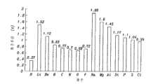
因为碳和硅原子之间的亲合性,对于DLC膜SiOXNy表现出良好的粘接性,形成Si-C键。另外,硅还被证实对于制造读写头所用的各种衬底材料具有好的粘接性,包括材料例如AlTiC、Al2O3、NiFe、NiFeCo和类似性质的其它材料。进一步,通过改变氧和氮的浓度,化学式中的x和y,能够定制氮氧化硅的化学、机械和物理特性。为了参考和比较,图1提供了在磁读写头制造中使用的各种材料的几种相关的机械和电学特性的表格。Because of the affinity between carbon and silicon atoms,SiOxNy exhibits good adhesion to DLC films, forming Si-C bonds. In addition, silicon has also been shown to have good adhesion toa variety of substrate materials used in the manufacture of read/write heads, including materials such as AlTiC,Al2O3 , NiFe, NiFeCo, and others of similar nature. Further, by changing the concentration of oxygen and nitrogen, x and y in the chemical formula, the chemical, mechanical and physical properties of silicon oxynitride can be tailored. For reference and comparison, Figure 1 provides a table of several relevant mechanical and electrical properties of various materials used in magnetic read-write head fabrication.
薄保护膜的重要功能,例如本发明的双层,是提供腐蚀保护。与硅或非晶硅相比,SiO2和Si3N4更加稳定且抗腐蚀并因此防腐蚀。例如,在碱性溶液中硅的蚀刻率比SiO2或Si3N4的都高得多;特别在KOH溶液中(重量百分数33.3%,80℃),Si在(100)面的蚀刻率为11000埃/分钟,而对于热氧化物(thermoxide)SiO2,大约77埃/分钟以及对于富含Si的氮化硅和按化学配比的氮化硅而言,蚀刻率基本上为零。(K.R.Wiliams,“Etch rate formicromachining processing-part II”Journal of Microelectromechanical Systems,12(67),pp.761-778,2003)。An important function of thin protective films, such as the double layer of the present invention, is to provide corrosion protection. Compared to silicon or amorphous silicon, SiO2 and Si3 N4 are more stable and corrosion resistant and thus corrosion resistant. For example, the etching rate of silicon in alkaline solution is much higher than that of SiO2 or Si3 N4 ; especially in KOH solution (33.3% by weight, 80°C), the etching rate of Si on the (100) plane is 11000 angstroms/min, and about 77 angstroms/min for thermoxideSiO2 and essentially zero for Si-rich silicon nitride and stoichiometric silicon nitride. (KR Wiliams, "Etch rate formicromachining processing-part II" Journal of Microelectromechanical Systems, 12(67), pp.761-778, 2003).
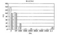
浸渍试验能够揭示保护覆盖层的抗腐蚀性。该试验在酸性(蚁酸)和碱性(小苏打)条件下被实施。具有相同的30埃的厚度,SiON/DLC双层在统计上显示出比传统的Si/DLC双层(见图3)高的抗腐蚀性。Immersion tests can reveal the corrosion resistance of protective coatings. The test was carried out under acidic (formic acid) and alkaline (baking soda) conditions. With the same thickness of 30 Angstroms, SiON/DLC bilayers show statistically higher corrosion resistance than conventional Si/DLC bilayers (see Figure 3).
SiOXNy的硬度能够从6Gpa(SiO2)变化到超过20Gpa(SiNy)。类似地,SiOXNy薄膜的应力能够从对于SiNy的+0.9Gpa的拉应力变化(调节)到对于SiO2的-0.3Gpa的压应力。通过比较,a-Si具有大约+1.0Gpa的压应力(R.T.Howe et al.,“Stress in polycrystalline and amorphous silicon thin films ”,Journal ofApplied Physics,54(8)pp.4674-4675,1983)。SiOXNy的其它特性的调节也被很好地说明,例如其光学反射系数能在对于SiO2的1.45到对于SiNy的2.0到对于富含Si的SiOXNy的2.4之间变化。The hardness of SiOx Ny can vary from 6 GPa (SiO2 ) to over 20 GPa (SiNy ). Similarly, the stress ofaSiOxNy film can be varied (tuned) from a tensile stress of +0.9 GPa forSiNy to a compressive stress of -0.3 GPa forSiO2 . By comparison, a-Si has a compressive stress of about +1.0 GPa (RT Howe et al., "Stress in polycrystalline and amorphous silicon thin films", Journal of Applied Physics, 54(8) pp.4674-4675, 1983). Tuning of other properties ofSiOxNy is also well described, for exampleits optical reflectance can be varied from 1.45 forSiO2 to 2.0 forSiNy to2.4 for Si-richSiOxNy .
上面所提到的,在下层和DLC层的总厚度减小到小于30埃的范围时,精确到每一个原子都值得保护。氧和氮在最小的原子之中(图4)。在非晶SiO2中,两个O原子大约占据一个Si原子的空间,所以对于给定的厚度能够插入更多小的原子。对于DLC覆盖层的耐磨性,覆盖层对衬底的粘接强度是重要的考虑因素。在本发明中耐磨性已通过用Hysitron Triboindenter纳米磨损实验得到证实。相同的20微牛的负载和20个磨损周期应用到相同厚度的常规Si/DLC双层和本发明的SiOXNy/DLC,本发明的SiOXNy/DLC表现出更好的纳米磨损耐久性。As mentioned above, when the total thickness of the underlayer and the DLC layer is reduced to a range of less than 30 Angstroms, every atom is worthy of protection. Oxygen and nitrogen are among the smallest atoms (Figure 4). In amorphousSiO2 , two O atoms occupy approximately the space of one Si atom, so more small atoms can be inserted for a given thickness. For the abrasion resistance of the DLC overlay, the bond strength of the overlay to the substrate is an important consideration. Wear resistance in the present invention has been confirmed by using Hysitron Triboindenter nano-abrasion experiments. The same load of 20 µN and 20 wear cycles were applied to conventional Si/DLC bilayers ofthe same thickness and the inventiveSiOxNy /DLC, the inventiveSiOxNy /DLC exhibited better nanowear durability.
因为SiON比Si更绝缘,表面分流及其相关噪音能被大大减少。图5显示了对传统Si/DLC双层(阴影条)和本发明的SiON/DLC双层(无阴影条)(每种的260个滑块)进行准静态测试(Quasi-Static Test)的结果,并且结果表明在SiON/DLC保护的滑块中爆米花噪音的频度明显减小。Because SiON is more insulating than Si, surface shunting and its associated noise can be greatly reduced. Figure 5 shows the results of a quasi-static test (Quasi-Static Test) on conventional Si/DLC bilayers (shaded bars) and SiON/DLC bilayers of the present invention (unshaded bars) (260 sliders each) , and the results show that the frequency of popcorn noise is significantly reduced in the SiON/DLC protected slider.
可以通过多种方法制备SiOXNy下层,包括:TheSiOxNyunderlayer can be prepared by a variety of methods, including:
1.在Ar/O2/N2气氛中以金属、金属氧化物或金属氮化物靶进行的反应性溅射Si。1. Reactive sputtering of Si with metal, metal oxide or metal nitride targets in an Ar/O2 /N2 atmosphere.
2.等离子体增强化学气相沉积(PECVD),低压力化学气相沉积(LPCVD),等离子体浸入离子注入(PIII),等离子体浸入离子注入沉积(PIIID)。2. Plasma Enhanced Chemical Vapor Deposition (PECVD), Low Pressure Chemical Vapor Deposition (LPCVD), Plasma Immersion Ion Implantation (PIII), Plasma Immersion Ion Implantation Deposition (PIIID).
3.通过离子束等离子体、电容性耦合等离子体(CCP)、电感耦合等离子体(ICP)和电子回旋共振(ECR)等离子体进行的Si表面的等离子体处理。3. Plasma treatment of Si surfaces by ion beam plasma, capacitively coupled plasma (CCP), inductively coupled plasma (ICP) and electron cyclotron resonance (ECR) plasma.
附图说明Description of drawings
从下面对优选实施例的描述的上下文中,本发明的目的、特征和优点将被理解。优选实施例的描述将在附图的上下文中被理解,其中:The objects, features and advantages of the invention will be understood from the context of the following description of the preferred embodiment. The description of preferred embodiments will be understood in the context of the accompanying drawings, in which:
图1是列出用于形成读写头及其保护层的材料的几种相关特性的表。Figure 1 is a table listing several relevant properties of the materials used to form the read/write head and its protective layer.
图2a和2b是描述形成本发明的保护双层的步骤的示意性流程图。Figures 2a and 2b are schematic flow charts describing the steps of forming the protective bilayer of the present invention.
图3展示了现有技术保护层与本发明保护层的腐蚀率的比较。Figure 3 shows a comparison of the corrosion rates of the prior art protective layer and the protective layer of the present invention.
图4显示了用于本发明的元素的原子半径。Fig. 4 shows the atomic radii of elements used in the present invention.
图5显示了与现有技术保护层相关的爆米花噪音和与本发明保护层相关的爆米花噪音之间的比较。Figure 5 shows a comparison between the popcorn noise associated with the prior art cover and the popcorn noise associated with the cover of the present invention.
图6是被本发明的双层所保护的读写头和磁盘之间界面的示意图。Figure 6 is a schematic diagram of the interface between a read-write head and a magnetic disk protected by a double layer of the present invention.
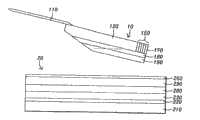
图7是使用离子束溅射、聚焦离子束溅射或脉冲离子束溅射的本发明优选实施例的示意图。Figure 7 is a schematic diagram of a preferred embodiment of the invention using ion beam sputtering, focused ion beam sputtering or pulsed ion beam sputtering.
图8是使用高能激光的本发明优选实施例的示意图。Figure 8 is a schematic diagram of a preferred embodiment of the invention using a high energy laser.
图9是本发明优选实施例的示意图,其中在多个读写头或磁介质上的溅射Si膜暴露于混合的Ar/O2/N2等离子体,顺序包括Ar/N2等离子体和Ar/O2等离子体(或相反顺序),其中该等离子体被作为电感耦合等离子体(ICP),电容性耦合等离子体(CCP),或电子回旋共振等离子体(electron cyclotronresonance,ECR)而应用。Figure 9 is a schematic diagram of a preferred embodiment of the invention in which sputtered Si films on multiple read/write heads or magnetic media are exposed to a mixed Ar/O2 /N2 plasma in a sequence comprising Ar/N2 plasma and Ar/O2 plasma (or in reverse order), where the plasma is applied as an inductively coupled plasma (ICP), capacitively coupled plasma (CCP), or electron cyclotron resonance (ECR) plasma.
具体实施方式Detailed ways
本发明的优选实施例教导在磁读写头或磁介质上制作一层薄的保护双层的方法,其中该保护双层包括SiOXNy增强粘性和抗腐蚀下层(underlayer),其上形成一层坚固的、类金刚石碳(DLC)保护覆盖层(也叫做保护层)。Preferred embodiments of the present invention teach a method of fabricating a thin protective bilayer on a magnetic read/ write head or magnetic media, wherein the protective bilayer includes aSiOxNy enhanced adhesion and corrosion resistant underlayer on which A strong, diamond-like carbon (DLC) protective covering (also called a cap).
在磁记录行业中非晶Si(a-Si)被广泛用作粘着层(adhesion layer)以提升DLC层对磁读写头衬底的粘着性。参照图2a,通过顺序的三个步骤图示出了现有技术中在读写头上形成保护覆盖层。在现有技术中,该覆盖过程以使用Ar+离子束对头衬底的清洁作为开始。接在此清洁工艺之后,使用离子束溅射沉积非晶Si的粘着层然后使用离子束沉积(IBD)或PECVD或,更加优选地,过滤阴极真空弧光(FCVA)沉积DLC覆盖层。Amorphous Si (a-Si) is widely used as an adhesion layer in the magnetic recording industry to improve the adhesion of the DLC layer to the substrate of the magnetic read/write head. Referring to Fig. 2a, the prior art formation of a protective overlay on a read/write head is illustrated through a sequence of three steps. In the prior art, the blanketing process starts with cleaning of the head substrate using an Ar+ ion beam. Following this cleaning process, an adhesion layer of amorphous Si is deposited using ion beam sputtering followed by a DLC capping layer using ion beam deposition (IBD) or PECVD or, more preferably, filtered cathodic vacuum arc (FCVA).
本发明的优选实施例不同于在读写头衬底上的a-Si的现有技术IBD沉积并且还将包括在包括磁记录介质和读写头的衬底上沉积。参照图2b,显示了制作本发明的保护双层的顺序的三个步骤。Preferred embodiments of the present invention differ from prior art IBD deposition of a-Si on head substrates and will also include deposition on substrates including magnetic recording media and heads. Referring to Figure 2b, there are shown three steps in the sequence of making the protective bilayer of the present invention.
1.使用Ar+离子束作为蚀刻装置(etching mechanism)对衬底预清洁,其中该衬底可以是读写头或磁介质的表面。1. Pre-cleaning the substrate, which can be the surface of a read-write head or a magnetic medium, using an Ar+ ion beam as an etching mechanism.
2.使用在Ar/O2/N2气氛中以硅、氧化硅或氮化硅靶进行的反应离子溅射Si,等离子增强化学气相沉积(PECVD),或反应脉冲激光沉积,来沉积增强粘着性和抗腐蚀的下层SiOXNy。或者通过离子束等离子体、电容性耦合等离子体(CCP)、电子回旋共振(ECR)等离子体、电感耦合等离子体(ICP)或通过等离子体浸入离子注入/沉积(PIIID),对a-Si膜进行等离子处理。2. Deposit enhanced adhesion using reactive ion sputtering of Si, plasma enhanced chemical vapor deposition (PECVD), or reactive pulsed laser deposition on silicon, silicon oxide, or silicon nitride targets in an Ar/O2 /N2 atmosphere and corrosion-resistant lower layer SiOX Ny . Or by ion beam plasma, capacitively coupled plasma (CCP), electron cyclotron resonance (ECR) plasma, inductively coupled plasma (ICP) or by plasma immersion ion implantation/deposition (PIIID), the a-Si film Perform plasma treatment.
3.使用离子束沉积(IBD)、等离子增强化学气相沉积(PECVD)或过滤阴极真空弧光(FCVA)沉积DLC的保护覆盖层。3. Deposit the protective overlay of the DLC using ion beam deposition (IBD), plasma enhanced chemical vapor deposition (PECVD), or filtered cathodic vacuum arc (FCVA).
本发明接下来的九个实施例都是在磁读写头或磁介质上形成保护双层的方法,其将满足本发明以上阐明的所有目的。在全部的实施例中,保护层形成在读写头或记录介质的合适的衬底表面上,例如已由合适的方法例如Ar+束蚀刻清洗的空气支承层表面(air-bearing layer surface,ABS)。还可以理解的是多个读写头优选地安装在夹具上并同时通过该方法处理。The next nine embodiments of the present invention are all methods of forming a protective double layer on a magnetic read-write head or magnetic media, which will meet all the objectives of the present invention set forth above. In all embodiments, the protective layer is formed on a suitable substrate surface of the read/write head or recording medium, such as an air-bearing layer surface (ABS) that has been cleaned by a suitable method such as Ar+ beam etching. ). It will also be appreciated that multiple read/write heads are preferably mounted on the fixture and processed by the method simultaneously.
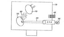
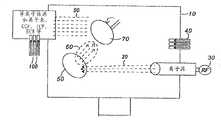
为了示意性地图示本发明下面任一实施例的应用的目的,,图6示意性地显示了在头和介质假设的位置中位于磁记录介质上方的读写头,而硬盘驱动器(HDD)在工作中并且该磁记录介质在该头下面移动。该图图示了磁头-盘界面(未按比例作图),其中磁读写头滑块(10)被机械地连接其悬臂(110)。该滑块设置在具有被屏蔽的GMR或TMR读取头和写入头(150)以及Al2O3覆盖层(170)的AlTiC衬底(120)上。读取头屏蔽、读取头和写入头材料主要由磁性材料形成,该磁性材料包括各种合金和Ni-Fe-Co化合物,其暴露在周围环境条件下时,可以抗腐蚀。该滑块涂敷有下层(180)和DLC覆盖层(190)。For the purpose of schematically illustrating the application of any of the following embodiments of the invention, Figure 6 schematically shows a read/write head above a magnetic recording medium in a hypothetical position of the head and medium, while a hard disk drive (HDD) is in In operation and the magnetic recording medium moves under the head. The figure illustrates the head-disk interface (not drawn to scale), where the magnetic head slider (10) is mechanically connected to its suspension (110). The slider is disposed onan AlTiC substrate (120) with shielded GMR or TMR read and write heads (150) and anAl2O3 capping layer (170). The read head shield, read head and write head materials are formed primarily of magnetic materials including various alloys and Ni-Fe-Co compounds that resist corrosion when exposed to ambient environmental conditions. The slider is coated with an underlayer (180) and a DLC overlay (190).
另一方面,在该滑块下旋转的磁记录介质(在这些实施例中的磁盘(20))被设置在玻璃或铝衬底(210)上,该衬底上是第一下层(220)(不是本发明的下层)和磁性层(230)。磁性层(230)的表面被第二下层(280)和DCL覆盖层(290)保护,该第二下层是本发明的下层,第二下层和DCL覆盖层都是通过本发明的方法形成的。为了减小对滑块头的磨损,润滑层(260)被应用在磁盘上。本发明提供用于滑块(180)和磁盘(280)以及形成于其上的下层和DLC层。On the other hand, the magnetic recording medium (disk (20) in these embodiments) that rotates under the slider is disposed on a glass or aluminum substrate (210) on which is a first lower layer (220 ) (not the lower layer of the present invention) and magnetic layer (230). The surface of the magnetic layer (230) is protected by a second lower layer (280) and a DCL covering layer (290), the second lower layer being the lower layer of the present invention, both the second lower layer and the DCL covering layer being formed by the method of the present invention. To reduce wear on the slider head, a lubricating layer (260) is applied on the disk. The present invention provides for the slider (180) and disk (280) and the underlying and DLC layers formed thereon.
第一优选实施例first preferred embodiment
参照图7,显示了具有在磁读写头或记录介质上形成本发明的保护双层的装置的示意性透视图。Referring to FIG. 7, there is shown a schematic perspective view of an apparatus having a protective bilayer of the present invention formed on a magnetic read/write head or a recording medium.
本发明第一优选实施例使用沉积室(10),在其中注入离子束,在本发明中是Ar+束(20)。该束由RF源(30)产生并由范围从300V到1200V的电压加速。注入端口(40)允许O2和N2气注入该室(10),该O2和N2气具有在0到20sccm之间的流速以及不同的比率,x/y,取决于SiOXNy下层的期望的形式。Ar+束对准SiO2溅射靶(50)并且被溅射的原子(60)撞击到可旋转的安装的沉积靶(70)上,该靶可以是读写头,多个该读写头作为未切割的滑块可以安装在可旋转的夹具上,该可旋转的夹具能够旋转用于沉积的均匀。可选择地,沉积靶(70)还可以是被类似安装的磁记录介质,例如图6的磁盘。所制作的下层具有x的值在0.02到2.0之间并且y的值在0.01到1.5之间可以满足本发明的目的。还指出x和y可以根据沉积过程的进行而变化以制作出粘着层,其成分是层厚度的函数。在所有这些形成中,不超过50埃的下层的全部厚度产生满足本发明目的的结果。下层厚度小于20埃是最优选的。下层沉积之后,在该下层上形成DLC层用来制作结合的双层以满足本发明的目的。A first preferred embodiment of the invention uses a deposition chamber (10) into which an ion beam, in this invention an Ar+ beam (20) is implanted. The beam is generated by an RF source (30) and accelerated by voltages ranging from 300V to 1200V. Injection port (40)allowsO2 andN2 gas to be injected into the chamber (10) with flow rates between 0 and 20 sccm anddifferent ratios, x/y, depending on SiOX Ny The desired form of the lower layer. The Ar+ beam is aimed at aSiO2 sputtering target (50) and the sputtered atoms (60) impinge on a rotatably mounted deposition target (70), which can be a read-write head, a plurality of which As uncut slides can be mounted on a rotatable fixture that can be rotated for uniformity of deposition. Alternatively, the deposition target ( 70 ) may also be a similarly mounted magnetic recording medium, such as the magnetic disk of FIG. 6 . Fabricating the lower layer with a value of x between 0.02 and 2.0 and a value of y between 0.01 and 1.5 can satisfy the purpose of the present invention. It is also pointed out that x and y can be varied according to the progress of the deposition process to make an adhesive layer whose composition is a function of layer thickness. In all of these formations, an overall thickness of the underlayer of not more than 50 angstroms produced results satisfactory for the purposes of the present invention. Underlayer thicknesses of less than 20 Angstroms are most preferred. After the lower layer is deposited, a DLC layer is formed on the lower layer to make a bonded bilayer for the purposes of the present invention.
第二优选实施例Second preferred embodiment
在第二优选实施例中,图8的装置被如上使用,但溅射靶材料(50)是Si3N4。离子束,在本实施例中是Ar+束(20),使用300V到1200V之间的电压将其注入并且O2和N2气被注入室(10)中,该O2和N2气具有0到20sccm之间的流速并且不同的比率,x/y,取决于SiOXNy下层的期望的形式。Ar+束对准Si3N4溅射靶(50)并且在注入的O2和N2气存在下溅射的Si和N原子(60)撞击到可旋转的安装的读写头的沉积靶(70)上用以产生所期望的SiOXNy下层。多个该读写头作为未切割的滑块可以安装在可旋转的夹具上以使得沉积均匀。可选择地,沉积靶(70)还可以是磁记录介质例如磁盘。所制作的下层具有x的值在0.02到2.0之间并且y的值在0.01到1.5之间可以满足本发明的目的。还指出x和y可以根据沉积过程的进行而变化以制作出下层,其成分是下层厚度的函数。在所有这些形成中,不超过50埃的下层的全部厚度产生满足本发明目的的结果。下层厚度小于20埃是最优选的。In a second preferred embodiment,the apparatus of Figure 8 is used as above, but the sputtering target material (50) isSi3N4 . An ion beam, in this example an Ar+ beam (20), is injected using a voltage between 300V and 1200V andO2 andN2 gas are injected into the chamber (10), theO2 andN2 gas having Flow rates between 0 and 20 seem and different ratios, x/y, depending on the desired form of theSiOxNyunderlayer .The Ar+ beam is aimed at theSi3N4 sputtering target (50) and the sputtered Si and N atoms (60) in the presence of injectedO2 andN2 gases impinge on the deposition target of the rotatably mounted read/write head (70) to produce the desired lower layer of SiOX Ny . Multiples of the read/write heads as uncut sliders can be mounted on a rotatable fixture for uniform deposition. Alternatively, the deposition target (70) may also be a magnetic recording medium such as a magnetic disk. Fabricating the lower layer with a value of x between 0.02 and 2.0 and a value of y between 0.01 and 1.5 can satisfy the purpose of the present invention. It is also pointed out that x and y can be varied as the deposition process proceeds to produce an underlying layer whose composition is a function of the thickness of the underlying layer. In all of these formations, an overall thickness of the underlayer of not more than 50 angstroms produced results satisfactory for the purposes of the present invention. Underlayer thicknesses of less than 20 Angstroms are most preferred.
下层形成之后,用上文所述方法在该下层上形成DLC覆盖层。After the lower layer is formed, a DLC capping layer is formed on the lower layer by the method described above.
第三优选实施例third preferred embodiment
本发明的第三优选实施例使用图7的装置,包括沉积室(10),其中当注入端口(40)允许O2和N2气以0到20sccm之间的流速以及取决于SiOXNy下层的期望形式的不同的比率x/y注入时,离子束能够注入到该沉积室中。然而,在本实施例中,离子束是高能扫描聚焦离子束(20),其对准Si的溅射靶(50)并且溅射的原子(60)撞击到可旋转的安装的读写头的沉积靶(70)上,该读写头作为未切割的滑块可以被安装在可旋转的夹具上以使得沉积均匀。可选择地,沉积靶(70)还可以是磁记录介质例如磁盘。为了避免毒化(poisoning)溅射靶并减小沉积所带来的滞后效应(hysteresis effect),使用如T.Nyberg等人所描述(美国专利申请2004/0149566,其全部内容在此被作为参考)的高能扫描聚焦的离子束。所制作的下层具有x的值在0.02到2.0之间并且y的值在0.01到1.5之间可以满足本发明的目的。还指出x和y可以根据沉积过程的进行而变化以制作出下层,其成分是下层厚度的函数。在所有这些形成中,不超过50埃的下层的全部厚度产生满足本发明目的的结果。下层厚度小于20埃是最优选的。A third preferred embodiment of the present invention uses the apparatus of Fig. 7, comprising a deposition chamber (10), wherein when the injection port (40) allows O2andN2 gas flow rates between 0and 20 sccm and depending onSiOxNy Ion beams can be implanted into the deposition chamber when different ratios x/y of the desired form of the underlying layer are implanted. In this example, however, the ion beam is a high energy scanned focused ion beam (20) which is aimed at a sputtering target (50) of Si and the sputtered atoms (60) impinge on the rotatably mounted read/write head. On the deposition target (70), the read/write head as an uncut slider can be mounted on a rotatable fixture to allow uniform deposition. Alternatively, the deposition target (70) may also be a magnetic recording medium such as a magnetic disk. To avoid poisoning the sputtering target and reduce the hysteresis effect caused by deposition, use as described by T. Nyberg et al. (US Patent Application 2004/0149566, the entire contents of which are hereby incorporated by reference) A high-energy scanning focused ion beam. Fabricating the lower layer with a value of x between 0.02 and 2.0 and a value of y between 0.01 and 1.5 can satisfy the purpose of the present invention. It is also pointed out that x and y can be varied as the deposition process proceeds to produce an underlying layer whose composition is a function of the thickness of the underlying layer. In all of these formations, an overall thickness of the underlayer of not more than 50 angstroms produced results satisfactory for the purposes of the present invention. Underlayer thicknesses of less than 20 Angstroms are most preferred.
第四优选实施例Fourth preferred embodiment
本发明的第四优选实施例使用图7的装置,包括沉积室(10),其中当注入端口(40)允许O2和N2气以0到20sccm之间的流速以及取决于SiOXNy下层的期望形式的不同的比率x/y注入时,离子束能够注入到该沉积室中。然而,在本实施例中,离子束(20)由具有高瞬时功率的脉冲离子源(30)产生,该束对准Si的溅射靶(50)并且溅射的原子(60)撞击到可旋转的安装的读写头的沉积靶(70)上,该读写头作为多个未切割的滑块被安装在可旋转的夹具上以使得沉积均匀。同样地,沉积靶(70)可以是被安装在夹具上的磁介质盘。为了避免毒化溅射靶并减小沉积所带来的滞后效应,使用如V.Kousnetsov等人所描述(美国专利号6,296,742,其全部内容在此被作为参考)的高瞬时功率的脉冲离子源。所制作的下层具有x的值在0.02到2.0之间并且y的值在0.01到1.5之间可以满足本发明的目的。还指出x和y可以根据沉积过程的进行而变化以制作出下层,其成分是下层厚度的函数。在所有这些形成中,不超过50埃的下层的全部厚度产生满足本发明目的的结果。下层厚度小于20埃是最优选的。A fourth preferred embodiment of the present invention uses the apparatus of Figure 7, comprising a deposition chamber (10) wherein when the injection port (40) allowsO2 andN2 gases to flow at between 0and 20 sccm and depending onSiOxNy Ion beams can be implanted into the deposition chamber when different ratios x/y of the desired form of the underlying layer are implanted. However, in this embodiment, the ion beam (20) is generated by a pulsed ion source (30) with high instantaneous power, the beam is aimed at the sputtering target (50) of Si and the sputtered atoms (60) hit the available On the deposition target (70) of a rotationally mounted read/write head mounted as a plurality of uncut sliders on a rotatable fixture to allow uniform deposition. Likewise, the deposition target (70) may be a magnetic media disk mounted on a fixture. To avoid poisoning the sputter target and reduce hysteresis effects from deposition, a high instantaneous power pulsed ion source was used as described by V. Kousnetsov et al. (US Patent No. 6,296,742, the entire contents of which are hereby incorporated by reference). Fabricating the lower layer with a value of x between 0.02 and 2.0 and a value of y between 0.01 and 1.5 can satisfy the purpose of the present invention. It is also pointed out that x and y can be varied as the deposition process proceeds to produce an underlying layer whose composition is a function of the thickness of the underlying layer. In all of these formations, an overall thickness of the underlayer of not more than 50 angstroms produced results satisfactory for the purposes of the present invention. Underlayer thicknesses of less than 20 Angstroms are most preferred.
第五优选实施例Fifth preferred embodiment
在本发明的第五优选实施例使用图8的装置,其包括沉积室(10),其中当注入端口(40)允许O2和N2气以在0到20sccm之间的流速以及取决于SiOXNy下层的期望形式的不同的比率x/y注入时,激光器(20)将电磁辐射波(80)对准Si、SiO2或Si3N4溅射靶(50)。在本实施例中,激光器可以是高能激光器例如CO2激光器、准分子激光器等等,并且由激光束射出的原子(60)撞击到可旋转的安装的读写头的沉积靶(70)上,该读写头作为未切割的滑块可以安装在可旋转的夹具上以使得沉积均匀。可选择地,沉积靶(70)还可以是磁记录介质,例如磁盘。激光通量可以在大约2到5J/cm2之间。所制作的下层具有x的值在0.02到2.0之间并且y的值在0.01到1.5之间可以满足本发明的目的。还指出x和y可以根据沉积过程的进行而变化以制作出下层,其成分是下层厚度的函数。在所有这些形成中,不超过50埃的下层的全部厚度产生满足本发明目的的结果。下层厚度小于20埃是最优选的。In a fifth preferred embodiment of the present invention the apparatus of Fig. 8 is used, which comprises a deposition chamber (10), wherein when the injection port (40) allows O2andN2 gases at flow rates between 0 and 20 sccm and depending on the SiO The laser ( 20 ) directs the electromagnetic radiation wave ( 80 ) at the Si, SiO2 or Si3 N4 sputtering target ( 50 ) upon implantation of different ratios x/y of the desired form of theX Ny lower layer. In this embodiment, the laser may be a high-energy laser such as aCO2 laser, an excimer laser, etc., and the atoms (60) emitted by the laser beam impinge on the deposition target (70) of the rotatably mounted read-write head, The read/write head as an uncut slider can be mounted on a rotatable fixture for uniform deposition. Alternatively, the deposition target (70) may also be a magnetic recording medium, such as a magnetic disk. The laser fluence can be between about 2 and 5 J/cm2 . Fabricating the lower layer with a value of x between 0.02 and 2.0 and a value of y between 0.01 and 1.5 can satisfy the purpose of the present invention. It is also pointed out that x and y can be varied as the deposition process proceeds to produce an underlying layer whose composition is a function of the thickness of the underlying layer. In all of these formations, an overall thickness of the underlayer of not more than 50 angstroms produced results satisfactory for the purposes of the present invention. Underlayer thicknesses of less than 20 Angstroms are most preferred.
第六优选实施例Sixth preferred embodiment
参照图9,显示了一种装置的示意性透视图,其中执行根据第六优选实施例在磁读写头上形成保护双层的两步过程。Referring to Figure 9, there is shown a schematic perspective view of an apparatus in which a two-step process of forming a protective bilayer on a magnetic read/write head according to a sixth preferred embodiment is performed.
本发明的第六优选实施例使用图9的沉积室(10),反应离子束,例如本实施例的Ar+束(20)注入到该沉积室中。该束由RF源(30)产生并由范围从300V到1200V的电压加速。该束(20)撞击Si溅射靶(50)产生即将溅射到可旋转的安装的沉积靶(70)上的Si原子,该沉积靶可以是多个可旋转地安装的磁读写头,典型地作为多个未被切割的滑块,安装在可旋转的夹具上用于均匀沉积。可选择地,沉积靶(70)还可以是可旋转地安装的磁记录介质,例如磁盘,以在其上进行沉积。A sixth preferred embodiment of the present invention uses the deposition chamber (10) of Figure 9 into which a reactive ion beam, such as the Ar+ beam (20) of this embodiment is implanted. The beam is generated by an RF source (30) and accelerated by voltages ranging from 300V to 1200V. The beam (20) impinging on a Si sputtering target (50) produces Si atoms to be sputtered onto a rotatably mounted deposition target (70), which may be a plurality of rotatably mounted magnetic read/write heads, Typically as multiple uncut slides, mounted on a rotatable fixture for uniform deposition. Alternatively, the deposition target (70) may also be a rotatably mounted magnetic recording medium, such as a magnetic disk, to be deposited thereon.
在读写头或盘上沉积Si溅射膜后,该Si膜暴露于Ar、O2和N2气(Ar作为载气)的等离子体(90),O2和N2气分别具有不同的比率,该比率取决于SiOXNy层所需要的形式(即构成对已沉积的Si膜的等离子体表面处理的过程)。通过使用本领域中公知的许多方法可以产生并应用该等离子体,例如通过离子束形成的等离子体,电容性耦合等离子体(CCP)的形成和应用,电子回旋共振(ECR)等离子体的形成或电感耦合等离子体(ICP)的形成和应用。After depositing the Si sputtered film on the read-write head or disk, the Si film is exposed to plasma (90) of Ar, O2 and N2 gases (Ar as carrier gas), O2 and N2 gases have different ratio, which depends on the desired form oftheSiOxNy layer (ie, the process constituting the plasma surface treatment of the deposited Si film). The plasma can be generated and applied by using a number of methods known in the art, such as plasma by ion beam formation, capacitively coupled plasma (CCP) formation and application, electron cyclotron resonance (ECR) plasma formation or Formation and application of inductively coupled plasma (ICP).
所制作的下层具有x的值在0.02到2.0之间并且y的值在0.01到1.5之间可以满足本发明的目的。还指出x和y可以根据沉积过程的进行而变化以制作出下层,其成分是下层厚度的函数。在所有这些形成中,不超过50埃的下层的全部厚度产生满足本发明目的的结果。下层厚度小于20埃是最优选的。Fabricating the lower layer with a value of x between 0.02 and 2.0 and a value of y between 0.01 and 1.5 can satisfy the purpose of the present invention. It is also pointed out that x and y can be varied as the deposition process proceeds to produce an underlying layer whose composition is a function of the thickness of the underlying layer. In all of these formations, an overall thickness of the underlayer of not more than 50 angstroms produced results satisfactory for the purposes of the present invention. Underlayer thicknesses of less than 20 Angstroms are most preferred.
第七优选实施例Seventh preferred embodiment
本发明的第七优选实施例使用图9的沉积室(10),离子束,例如本实施例的Ar+束(20)注入到该沉积室中。该束由RF源(30)产生并由范围从300V到1200V的电压加速。该束(20)撞击Si溅射靶(50)产生即将溅射到可旋转的安装的沉积靶(70)上的Si原子,该沉积靶可以是多个可旋转的安装的磁读写头,典型地作为多个未被切割的滑块,安装在可旋转的夹具上用于均匀沉积。可选择地,溅射靶(70)可以是安装在可旋转的夹具上的磁介质,例如磁盘,并在其上进行沉积。A seventh preferred embodiment of the present invention uses the deposition chamber (10) of Figure 9 into which an ion beam, such as the Ar+ beam (20) of this embodiment is implanted. The beam is generated by an RF source (30) and accelerated by voltages ranging from 300V to 1200V. The beam (20) impinging on the Si sputtering target (50) produces Si atoms to be sputtered onto a rotatably mounted deposition target (70), which may be a plurality of rotatably mounted magnetic read/write heads, Typically as multiple uncut slides, mounted on a rotatable fixture for uniform deposition. Alternatively, the sputtering target (70) may be a magnetic medium, such as a magnetic disk, mounted on a rotatable holder and deposited thereon.
在读写头上沉积Si溅射膜后,接着该膜暴露于Ar/O2气的等离子体(90),紧接着暴露于Ar/N2气的等离子体,或可选择地,Ar/N2气的等离子体(90)紧接着Ar/O2气的等离子体的相反顺序。这些等离子体通过使用例如第六优选实施例所描述的方法形成,例如通过离子束形成的等离子体,电容性耦合等离子体(CCP)的形成和应用,电子回旋共振(ECR)等离子体的形成或电感耦合等离子体(ICP)的形成和应用,每个等离子体以不同的时间长度施加在Si膜上,取决于SiOXNy的期望的形式。所制作的下层具有x的值在0.02到2.0之间并且y的值在0.01到1.5之间可以满足本发明的目的。还指出x和y可以根据沉积过程的进行而变化以制作出下层,其成分是下层厚度的函数。在所有这些形成中,不超过50埃的下层的全部厚度产生满足本发明目的的结果。下层厚度小于20埃是最优选的。After deposition of the Si sputtered film on the read/write head, the film is then exposed to a plasma of Ar/O2 gas (90), followed by a plasma of Ar/N2 gas, or alternatively, Ar/N The plasma of2 gas (90) follows the reverse order of the plasma of Ar/O2 gas. These plasmas are formed using methods such as those described in the sixth preferred embodiment, such as plasmas formed by ion beams, the formation and application of capacitively coupled plasmas (CCP), the formation of electron cyclotron resonance (ECR) plasmas or Formation and application of inductively coupled plasmas (ICPs), each plasma is applied to the Si film for different lengths of time, depending onthe desired form ofSiOxNy . Fabricating the lower layer with a value of x between 0.02 and 2.0 and a value of y between 0.01 and 1.5 can satisfy the purpose of the present invention. It is also pointed out that x and y can be varied as the deposition process proceeds to produce an underlying layer whose composition is a function of the thickness of the underlying layer. In all of these formations, an overall thickness of the underlayer of not more than 50 angstroms produced results satisfactory for the purposes of the present invention. Underlayer thicknesses of less than 20 Angstroms are most preferred.
第八优选实施例Eighth preferred embodiment
本发明的第八优选实施例使用图9的沉积室(10),离子束,例如本实施例的Ar+束(20)注入到该沉积室中。该束由RF源(30)产生并由范围从300V到1200V的电压加速。该束(20)撞击到Si溅射靶(50)上产生即将溅射到可旋转的安装的沉积靶(70)上的Si原子,该沉积靶可以是多个可旋转地安装的磁读写头,典型地作为多个未被切割的滑块,安装在可旋转的夹具上用于均匀沉积。可选择地,沉积靶(70)可以是可旋转地安装的磁介质,例如磁盘,并在其上进行沉积。An eighth preferred embodiment of the present invention uses the deposition chamber (10) of Figure 9 into which an ion beam, such as the Ar+ beam (20) of this embodiment is implanted. The beam is generated by an RF source (30) and accelerated by voltages ranging from 300V to 1200V. The beam (20) impinges on the Si sputtering target (50) to produce Si atoms to be sputtered onto a rotatably mounted deposition target (70), which may be a plurality of rotatably mounted magnetic read/write The head, typically as multiple uncut slides, is mounted on a rotatable fixture for uniform deposition. Alternatively, the deposition target (70) may be a rotatably mounted magnetic medium, such as a magnetic disk, on which deposition is performed.
在读写头上沉积Si溅射膜以等离子体浸入沉积的形式,也就是说,沉积是在Ar、O2和N2气的等离子体(90)存在的情况下实施的,该等离子体通过使用例如第六优选实施例所描述的方法形成,例如由离子束形成的等离子体,电容性耦合等离子体(CCP)的形成和应用,电子回旋共振(ECR)等离子体的形成或电感耦合等离子体(ICP)的形成和应用,以及该等离子体以不同的O2和N2气的比率施加在室(10)内,该比率取决于SiOXNy层的期望的形式。所制作的下层具有x的值在0.02到2.0之间并且y的值在0.01到1.5之间可以满足本发明的目的。还指出x和y可以根据沉积过程的进行而变化以制作出粘着层,其成分是下层厚度的函数。在所有这些形成中,不超过50埃的下层的全部厚度产生满足本发明目的的结果。下层厚度小于20埃是最优选的。The Si sputtered film is deposited on the read/write head in the form of plasma immersion deposition, that is, the deposition is carried out in the presence of a plasma (90) of Ar,O2 andN2 gases, which is passed through Formed using methods such as those described in the sixth preferred embodiment, such as plasmas formed from ion beams, the formation and application of capacitively coupled plasmas (CCP), the formation of electron cyclotron resonance (ECR) plasmas or inductively coupled plasmas (ICP) formation and application, and the plasma is applied in the chamber (10) at different ratios ofO2 andN2 gases, depending on the desired form oftheSiOxNy layer. Fabricating the lower layer with a value of x between 0.02 and 2.0 and a value of y between 0.01 and 1.5 can satisfy the purpose of the present invention. It is also noted that x and y can be varied as the deposition process proceeds to create an adhesive layer whose composition is a function of the thickness of the underlying layer. In all of these formations, an overall thickness of the underlayer of not more than 50 angstroms produced results satisfactory for the purposes of the present invention. Underlayer thicknesses of less than 20 Angstroms are most preferred.
第九优选实施例Ninth preferred embodiment
再参照图7,显示了一种装置的示意性透视图,其中执行根据第九优选实施例在磁读写头上形成保护双层的两步过程。Referring again to FIG. 7 , there is shown a schematic perspective view of an apparatus in which a two-step process of forming a protective bilayer on a magnetic read/write head according to a ninth preferred embodiment is performed.
本发明的第九优选实施例使用图7的沉积室(10),反应离子束,例如本实施例的Ar+束(20)注入到该沉积室中。该束由RF源(30)产生并由范围从300V到1200V的电压加速。该束(20)撞击到Si溅射靶(50)上产生即将溅射到可旋转的安装的沉积靶(70)上的Si原子,该沉积靶可以是多个可旋转地安装的磁读写头,典型地以多个未被切割的滑块的形式,安装在可旋转的夹具上用于均匀沉积。可选择地,在其上进行沉积时,沉积靶(70)可以是安装在夹具上的用于在其上进行沉积的的磁介质,例如磁盘。A ninth preferred embodiment of the present invention uses the deposition chamber (10) of Figure 7 into which a reactive ion beam, such as the Ar+ beam (20) of this embodiment is implanted. The beam is generated by an RF source (30) and accelerated by voltages ranging from 300V to 1200V. The beam (20) impinges on the Si sputtering target (50) to produce Si atoms to be sputtered onto a rotatably mounted deposition target (70), which may be a plurality of rotatably mounted magnetic read/write The head, typically in the form of a plurality of uncut slides, is mounted on a rotatable fixture for uniform deposition. Alternatively, the deposition target ( 70 ) may be a magnetic medium, such as a magnetic disk, mounted on a fixture for deposition thereon when deposition is performed thereon.
在读写头上沉积Si溅射膜后,该Si膜暴露于O2和N2气氛,该O2和N2气以不同的x/y比率和不同的时间长度被引入室内,以使得Si膜的氧和氮能够取得SiOXNy形式的粘着层中所需要的x和y的值。所制作的下层具有x的值在0.02到2.0之间并且y的值在0.01到1.5之间可以满足本发明的目的。还指出x和y可以根据沉积过程的进行而变化以制作出下层,其成分是下层厚度的函数。在所有这些形成中,不超过50埃的下层的全部厚度产生满足本发明目的的结果。下层厚度小于20埃是最优选的。After depositing the Si sputtered film on theread /write head, the Si film is exposed toO2 andN2 atmospheres, which are introduced into the chamber at different x/y ratios and fordifferent lengths of time, so that the Si The oxygen and nitrogen of the film can achieve the values of x and y required inan adhesion layer of the formSiOxNy . Fabricating the lower layer with a value of x between 0.02 and 2.0 and a value of y between 0.01 and 1.5 can satisfy the purpose of the present invention. It is also pointed out that x and y can be varied as the deposition process proceeds to produce an underlying layer whose composition is a function of the thickness of the underlying layer. In all of these formations, an overall thickness of the underlayer of not more than 50 angstroms produced results satisfactory for the purposes of the present invention. Underlayer thicknesses of less than 20 Angstroms are most preferred.
本领域技术人员知道,本发明的优选实施例只是对本发明的说明并不是对本发明的限定。在仍然提供根据所附权利要求定义的本发明所形成保护层的情况下,可以对在磁读写头上形成保护层的方法,工艺,材料,结构和尺寸进行修改和变形。Those skilled in the art know that the preferred embodiments of the present invention are only for the description of the present invention and not for limiting the present invention. Modifications and variations may be made to the method, process, materials, structure and dimensions of forming a protective layer on a magnetic read/write head while still providing a protective layer formed in accordance with the present invention as defined in the appended claims.
Claims (34)
Applications Claiming Priority (2)
| Application Number | Priority Date | Filing Date | Title |
|---|---|---|---|
| US11/702,247 | 2007-02-05 | ||
| US11/702,247US20080187781A1 (en) | 2007-02-05 | 2007-02-05 | Magnetic recording head and media overcoat |
Publications (1)
| Publication Number | Publication Date |
|---|---|
| CN101303860Atrue CN101303860A (en) | 2008-11-12 |
Family
ID=39676425
Family Applications (1)
| Application Number | Title | Priority Date | Filing Date |
|---|---|---|---|
| CNA2008101277923APendingCN101303860A (en) | 2007-02-05 | 2008-02-05 | Protected magnetic read write head or magnetic recording medium and method of forming same |
Country Status (4)
| Country | Link |
|---|---|
| US (1) | US20080187781A1 (en) |
| JP (1) | JP2008192288A (en) |
| KR (1) | KR20080073258A (en) |
| CN (1) | CN101303860A (en) |
Cited By (7)
| Publication number | Priority date | Publication date | Assignee | Title |
|---|---|---|---|---|
| CN102157324A (en)* | 2009-12-14 | 2011-08-17 | Spp处理技术系统英国有限公司 | Ion beam source |
| CN102354659A (en)* | 2011-11-02 | 2012-02-15 | 上海宏力半导体制造有限公司 | Method for eliminating nucleation on mask and selective epitaxial growth method |
| CN104054129A (en)* | 2012-05-07 | 2014-09-17 | 富士电机株式会社 | Recording medium |
| CN104170014A (en)* | 2012-09-14 | 2014-11-26 | 富士电机株式会社 | Manufacturing method of magnetic recording medium |
| CN106929800A (en)* | 2017-04-24 | 2017-07-07 | 信利光电股份有限公司 | A kind of diamond-like carbon composite film and preparation method thereof |
| CN108315701A (en)* | 2017-01-16 | 2018-07-24 | 中国南玻集团股份有限公司 | The method that coating material and ion beam source deposition prepare coating material |
| CN108315700A (en)* | 2017-01-16 | 2018-07-24 | 中国南玻集团股份有限公司 | The method that coating material and ion beam source deposition prepare coating material |
Families Citing this family (12)
| Publication number | Priority date | Publication date | Assignee | Title |
|---|---|---|---|---|
| US8014104B2 (en)* | 2007-03-21 | 2011-09-06 | Sae Magnetics (Hk) Ltd. | Magnetic head/disk with transition metal oxynitride adhesion/corrosion barrier and diamond-like carbon overcoat bilayer |
| US20110058279A1 (en)* | 2009-07-31 | 2011-03-10 | Flint Eric | Overcoat having a low silicon/carbon ratio |
| US8968535B2 (en)* | 2009-12-14 | 2015-03-03 | Spp Process Technology Systems Uk Limited | Ion beam source |
| US8472134B2 (en) | 2011-08-02 | 2013-06-25 | HGST Netherlands B.V. | Air bearing surface overcoat with soft intermediate film, and methods of producing the same |
| US8687323B2 (en) | 2011-10-12 | 2014-04-01 | HGST Netherlands B.V. | Magnetic media disk anticorrosion overcoat with titanium and silicon based layers |
| WO2013138472A1 (en)* | 2012-03-16 | 2013-09-19 | The Trustees Of The University Of Pennsylvania | Method and material for protecting magnetic information storage media |
| JP6083154B2 (en) | 2012-08-30 | 2017-02-22 | 富士電機株式会社 | Magnetic recording medium |
| US9117619B2 (en)* | 2013-11-07 | 2015-08-25 | Electronics And Telecommunications Research Institute | Device for generating heavy-ion beam and method thereof |
| US9805748B1 (en) | 2014-06-24 | 2017-10-31 | Western Digital (Fremont), Llc | System and method for providing a protective layer having a graded intermediate layer |
| US9406323B2 (en)* | 2014-12-05 | 2016-08-02 | HGST Netherlands B.V. | Slider with aluminum compound fill |
| US11114122B1 (en)* | 2019-03-06 | 2021-09-07 | Seagate Technology Llc | Magnetic devices with overcoat that includes a titanium oxynitride layer |
| US12400680B1 (en) | 2024-05-01 | 2025-08-26 | Western Digital Technologies, Inc. | Head and media overcoats for heat assisted magnetic recording |
Family Cites Families (14)
| Publication number | Priority date | Publication date | Assignee | Title |
|---|---|---|---|---|
| US5070036A (en)* | 1989-01-04 | 1991-12-03 | Quality Microcircuits Corporation | Process for contacting and interconnecting semiconductor devices within an integrated circuit |
| US5227196A (en)* | 1989-02-16 | 1993-07-13 | Semiconductor Energy Laboratory Co., Ltd. | Method of forming a carbon film on a substrate made of an oxide material |
| US5609948A (en)* | 1992-08-21 | 1997-03-11 | Minnesota Mining And Manufacturing Company | Laminate containing diamond-like carbon and thin-film magnetic head assembly formed thereon |
| US5637373A (en)* | 1992-11-19 | 1997-06-10 | Semiconductor Energy Laboratory Co., Ltd. | Magnetic recording medium |
| JPH0845045A (en)* | 1994-07-29 | 1996-02-16 | Fujitsu Ltd | Magnetic head and manufacturing method thereof |
| JPH09212814A (en)* | 1996-01-31 | 1997-08-15 | Nec Corp | Protective film and magnetic head slider having protective film, as well as magnetic disk device |
| SE9704607D0 (en)* | 1997-12-09 | 1997-12-09 | Chemfilt R & D Ab | A method and apparatus for magnetically enhanced sputtering |
| US6136421A (en)* | 1998-07-21 | 2000-10-24 | Seagate Technology Llc | Magneto-resistance recording media comprising multilayered protective overcoats |
| US6569295B2 (en)* | 2001-03-20 | 2003-05-27 | International Business Machines Corporation | Method for grading surface topography for improved step coverage and planarization |
| SE521095C2 (en)* | 2001-06-08 | 2003-09-30 | Cardinal Cg Co | Reactive sputtering process |
| JP2003110337A (en)* | 2001-09-28 | 2003-04-11 | Mitsumi Electric Co Ltd | Four-point-fed loop antenna |
| US7300556B2 (en)* | 2003-08-29 | 2007-11-27 | Hitachi Global Storage Technologies Netherlands B.V. | Method for depositing a thin film adhesion layer |
| JP4039678B2 (en)* | 2005-08-22 | 2008-01-30 | アルプス電気株式会社 | Thin film magnetic head |
| US7758982B2 (en)* | 2005-09-02 | 2010-07-20 | Hitachi Global Storage Technologies Netherlands B.V. | SiN overcoat for perpendicular magnetic recording media |
- 2007
- 2007-02-05USUS11/702,247patent/US20080187781A1/ennot_activeAbandoned
- 2008
- 2008-02-04JPJP2008024433Apatent/JP2008192288A/enactivePending
- 2008-02-05KRKR1020080011881Apatent/KR20080073258A/ennot_activeWithdrawn
- 2008-02-05CNCNA2008101277923Apatent/CN101303860A/enactivePending
Cited By (12)
| Publication number | Priority date | Publication date | Assignee | Title |
|---|---|---|---|---|
| CN102157324A (en)* | 2009-12-14 | 2011-08-17 | Spp处理技术系统英国有限公司 | Ion beam source |
| TWI506664B (en)* | 2009-12-14 | 2015-11-01 | Spp Process Technology Systems Uk Ltd | Ion beam source, and apparatus for sputtering a non-conductive material |
| CN102354659A (en)* | 2011-11-02 | 2012-02-15 | 上海宏力半导体制造有限公司 | Method for eliminating nucleation on mask and selective epitaxial growth method |
| CN102354659B (en)* | 2011-11-02 | 2016-05-11 | 上海华虹宏力半导体制造有限公司 | Mask nucleation removing method and selective epitaxial growth method |
| CN104054129A (en)* | 2012-05-07 | 2014-09-17 | 富士电机株式会社 | Recording medium |
| CN104054129B (en)* | 2012-05-07 | 2015-09-02 | 富士电机株式会社 | Recording medium |
| CN104170014A (en)* | 2012-09-14 | 2014-11-26 | 富士电机株式会社 | Manufacturing method of magnetic recording medium |
| CN104170014B (en)* | 2012-09-14 | 2015-12-09 | 富士电机株式会社 | Manufacturing method of magnetic recording medium |
| US9758873B2 (en) | 2012-09-14 | 2017-09-12 | Fuji Electric Co., Ltd. | Manufacturing method for magnetic recording medium |
| CN108315701A (en)* | 2017-01-16 | 2018-07-24 | 中国南玻集团股份有限公司 | The method that coating material and ion beam source deposition prepare coating material |
| CN108315700A (en)* | 2017-01-16 | 2018-07-24 | 中国南玻集团股份有限公司 | The method that coating material and ion beam source deposition prepare coating material |
| CN106929800A (en)* | 2017-04-24 | 2017-07-07 | 信利光电股份有限公司 | A kind of diamond-like carbon composite film and preparation method thereof |
Also Published As
| Publication number | Publication date |
|---|---|
| JP2008192288A (en) | 2008-08-21 |
| US20080187781A1 (en) | 2008-08-07 |
| KR20080073258A (en) | 2008-08-08 |
Similar Documents
| Publication | Publication Date | Title |
|---|---|---|
| CN101303860A (en) | Protected magnetic read write head or magnetic recording medium and method of forming same | |
| US8009387B2 (en) | Forming an aluminum alloy oxynitride underlayer and a diamond-like carbon overcoat to protect a magnetic recording head and/or media | |
| US8014104B2 (en) | Magnetic head/disk with transition metal oxynitride adhesion/corrosion barrier and diamond-like carbon overcoat bilayer | |
| US5864452A (en) | Thin-film magnetic head and method of forming carbon film | |
| US9040125B2 (en) | Covalently bound monolayer for a protective carbon overcoat | |
| JP4335744B2 (en) | Magnetic head | |
| US20130033779A1 (en) | Air bearing surface overcoat with soft intermediate film, and methods of producing the same | |
| US20080316656A1 (en) | Magnetic head and method of manufacturing the magnetic head | |
| US6974642B2 (en) | Carbonaceous protective layer, magnetic recording medium, production method thereof, and magnetic disk apparatus | |
| US8420159B2 (en) | Method of fabricating magnetic head slider including partial removal step of protecting film | |
| US7280312B2 (en) | Method for producing a protective thin film for a magnetic head | |
| CN100370521C (en) | Thin film magnetic head, method of manufacturing the same, gimbal assembly having the thin film magnetic head, and magnetic disk apparatus | |
| HK1120917A (en) | Magnetic recording head and media overcoat | |
| US7283326B2 (en) | Methods for producing a protective film on recording media | |
| JP2000212738A (en) | Magnetron sputtering method and production of magnetic recording medium | |
| JP2900923B2 (en) | Magnetic head slider and method of manufacturing the same | |
| CN101887730A (en) | Method for manufacturing magnetic head slider | |
| JP2011192320A (en) | Perpendicular magnetic recording medium | |
| WO2015122847A1 (en) | An improved magnetic recording medium | |
| JP2005302185A (en) | Thin-film magnetic head device, head gimbal assembly equipped with the same, magnetic disk device equipped with head gimbal assembly, and method for manufacturing thin-film magnetic head device | |
| HK1116291A (en) | Magnetic recording head and media comprising aluminum oxynitride underlayer and a diamond-like carbon overcoat | |
| HK1118940A (en) | Metal oxynitride adhesion/corrosion barrier layer and a diamond-like carbon overcoat | |
| CN117223056A (en) | Magnetic recording medium with plasma polished pre-seed layer or substrate | |
| Choong et al. | Overcoat Materials for Magnetic Recording Media | |
| JP2004087042A (en) | Lubricant application method, lubricant layer, magnetic recording medium, and magnetic disk drive |
Legal Events
| Date | Code | Title | Description |
|---|---|---|---|
| C06 | Publication | ||
| PB01 | Publication | ||
| REG | Reference to a national code | Ref country code:HK Ref legal event code:DE Ref document number:1120917 Country of ref document:HK | |
| C02 | Deemed withdrawal of patent application after publication (patent law 2001) | ||
| WD01 | Invention patent application deemed withdrawn after publication | Open date:20081112 | |
| REG | Reference to a national code | Ref country code:HK Ref legal event code:WD Ref document number:1120917 Country of ref document:HK |