CN101303747A - Crossed double tags and RFID systems using crossed double tags - Google Patents
Crossed double tags and RFID systems using crossed double tagsDownload PDFInfo
- Publication number
- CN101303747A CN101303747ACNA2008100964232ACN200810096423ACN101303747ACN 101303747 ACN101303747 ACN 101303747ACN A2008100964232 ACNA2008100964232 ACN A2008100964232ACN 200810096423 ACN200810096423 ACN 200810096423ACN 101303747 ACN101303747 ACN 101303747A
- Authority
- CN
- China
- Prior art keywords
- tag
- label
- dipole antenna
- reader
- writer
- Prior art date
- Legal status (The legal status is an assumption and is not a legal conclusion. Google has not performed a legal analysis and makes no representation as to the accuracy of the status listed.)
- Granted
Links
Images


Classifications
- H—ELECTRICITY
- H01—ELECTRIC ELEMENTS
- H01Q—ANTENNAS, i.e. RADIO AERIALS
- H01Q9/00—Electrically-short antennas having dimensions not more than twice the operating wavelength and consisting of conductive active radiating elements
- H01Q9/04—Resonant antennas
- H01Q9/16—Resonant antennas with feed intermediate between the extremities of the antenna, e.g. centre-fed dipole
- H01Q9/28—Conical, cylindrical, cage, strip, gauze, or like elements having an extended radiating surface; Elements comprising two conical surfaces having collinear axes and adjacent apices and fed by two-conductor transmission lines
- H01Q9/285—Planar dipole
- G—PHYSICS
- G06—COMPUTING OR CALCULATING; COUNTING
- G06K—GRAPHICAL DATA READING; PRESENTATION OF DATA; RECORD CARRIERS; HANDLING RECORD CARRIERS
- G06K19/00—Record carriers for use with machines and with at least a part designed to carry digital markings
- G06K19/06—Record carriers for use with machines and with at least a part designed to carry digital markings characterised by the kind of the digital marking, e.g. shape, nature, code
- G06K19/067—Record carriers with conductive marks, printed circuits or semiconductor circuit elements, e.g. credit or identity cards also with resonating or responding marks without active components
- G06K19/07—Record carriers with conductive marks, printed circuits or semiconductor circuit elements, e.g. credit or identity cards also with resonating or responding marks without active components with integrated circuit chips
- G06K19/077—Constructional details, e.g. mounting of circuits in the carrier
- G06K19/07749—Constructional details, e.g. mounting of circuits in the carrier the record carrier being capable of non-contact communication, e.g. constructional details of the antenna of a non-contact smart card
- H—ELECTRICITY
- H01—ELECTRIC ELEMENTS
- H01Q—ANTENNAS, i.e. RADIO AERIALS
- H01Q1/00—Details of, or arrangements associated with, antennas
- H01Q1/12—Supports; Mounting means
- H01Q1/22—Supports; Mounting means by structural association with other equipment or articles
- H01Q1/2208—Supports; Mounting means by structural association with other equipment or articles associated with components used in interrogation type services, i.e. in systems for information exchange between an interrogator/reader and a tag/transponder, e.g. in Radio Frequency Identification [RFID] systems
- H01Q1/2225—Supports; Mounting means by structural association with other equipment or articles associated with components used in interrogation type services, i.e. in systems for information exchange between an interrogator/reader and a tag/transponder, e.g. in Radio Frequency Identification [RFID] systems used in active tags, i.e. provided with its own power source or in passive tags, i.e. deriving power from RF signal
- H—ELECTRICITY
- H01—ELECTRIC ELEMENTS
- H01Q—ANTENNAS, i.e. RADIO AERIALS
- H01Q21/00—Antenna arrays or systems
- H01Q21/24—Combinations of antenna units polarised in different directions for transmitting or receiving circularly and elliptically polarised waves or waves linearly polarised in any direction
- H01Q21/26—Turnstile or like antennas comprising arrangements of three or more elongated elements disposed radially and symmetrically in a horizontal plane about a common centre
- H—ELECTRICITY
- H01—ELECTRIC ELEMENTS
- H01Q—ANTENNAS, i.e. RADIO AERIALS
- H01Q9/00—Electrically-short antennas having dimensions not more than twice the operating wavelength and consisting of conductive active radiating elements
- H01Q9/04—Resonant antennas
- H01Q9/16—Resonant antennas with feed intermediate between the extremities of the antenna, e.g. centre-fed dipole
- H01Q9/26—Resonant antennas with feed intermediate between the extremities of the antenna, e.g. centre-fed dipole with folded element or elements, the folded parts being spaced apart a small fraction of operating wavelength
Landscapes
- Engineering & Computer Science (AREA)
- Computer Hardware Design (AREA)
- Microelectronics & Electronic Packaging (AREA)
- Physics & Mathematics (AREA)
- General Physics & Mathematics (AREA)
- Theoretical Computer Science (AREA)
- Near-Field Transmission Systems (AREA)
- Variable-Direction Aerials And Aerial Arrays (AREA)
Abstract
Translated fromChinese
Description
Translated fromChinese技术领域technical field
本发明涉及一种通过将两个线性偏振波标签以直角(right angle)交叉来延伸其与读/写器的通信距离的交叉双标签(crossed dual tag),并涉及一种使用该交叉双标签的RFID(射频识别)系统。The present invention relates to a crossed dual tag which extends its communication distance with a reader/writer by crossing two linearly polarized wave tags at a right angle, and relates to a crossed dual tag using the crossed dual tag. RFID (radio frequency identification) system.
背景技术Background technique
传统上,将RFID系统作为非接触认证技术运用在实际使用中,该非接触认证技术用于在RFID的IC(集成电路)芯片中记录与个人或对象有关的信息的各个条目,并且用于通过读/写器来无线地读取信息。Traditionally, the RFID system has been used in practical use as a non-contact authentication technology for recording individual items of information related to individuals or objects in IC (Integrated Circuit) chips of RFID, and for passing Reader/writer to read information wirelessly.
虽然以各种方式来称呼RFID,但是一般将RFID称为无线标签或仅称为标签。Although RFID is called in various ways, RFID is generally called a wireless tag or just a tag.
标签包括在厚度为大约0.1mm的薄片(sheet)、薄膜(film)等的平面上形成的金属天线,以及连接到该天线的馈电点(feeding point)的IC芯片。The tag includes a metal antenna formed on a plane of a sheet, film, or the like with a thickness of about 0.1 mm, and an IC chip connected to a feeding point of the antenna.
通常,IC芯片非常小,其厚度和面积大小分别在0.2mm和1平方毫米的数量级。将连接到IC芯片的天线形成为双极天线(dipole antenna)图案,而且该天线通过谐振(resonant)电流所生成的通信波是线性偏振波。Typically, IC chips are very small, with a thickness and area of the order of 0.2 mm and 1 square millimeter, respectively. An antenna connected to an IC chip is formed in a dipole antenna pattern, and a communication wave generated by the antenna through a resonant current is a linearly polarized wave.
在RFID系统中,读/写器发送大约1W的无线电波信号,标签侧接收该信号并将IC芯片内的信息作为响应信号返回给读/写器侧,并且读/写器读取该信息。In the RFID system, the reader/writer sends a radio wave signal of about 1W, the tag side receives the signal and returns the information inside the IC chip as a response signal to the reader/writer side, and the reader/writer reads the information.
标签不包括电池。当标签接近读/写器时,通过标签的天线与读/写器发射的无线电波的谐振来生成电流。IC芯片的电路只在此时工作,以将其中的信息发送到读/写器。Labels do not include batteries. When the tag approaches the reader/writer, a current is generated by the resonance of the tag's antenna with the radio waves emitted by the reader/writer. The circuits of the IC chip work only at this time to send the information in it to the reader/writer.
读/写器侧的天线被形成用来发射圆偏振无线电波,以使得对于任何方向的标签定向(orientation)都能够与生成用于其自身通信的线性偏振波的标签进行通信。The antenna on the reader/writer side is formed to emit circularly polarized radio waves to enable communication with a tag generating linearly polarized waves for its own communication for any orientation of the tag.
应用从860到960MHz的UHF(超高频)作为用于该发送的无线电波。例如,在日本使用952到954MHz的UHF。UHF (Ultra High Frequency) from 860 to 960 MHz is applied as radio waves for this transmission. For example, UHF of 952 to 954 MHz is used in Japan.
虽然读/写器与标签之间的通信距离取决于标签天线的增益、IC芯片的工作电压、周围环境等,但是在理想条件下该通信距离大约是3到5m。Although the communication distance between the reader/writer and the tag depends on the gain of the tag antenna, the operating voltage of the IC chip, the surrounding environment, etc., the communication distance is about 3 to 5m under ideal conditions.
读/写器的天线通过使用圆偏振无线电波来进行通信,而标签的天线通过使用线性偏振波来进行通信。因此,通过与从读/写器接收的无线电波的谐振而产生的功率(即,从读/写器接收的功率)是在假定标签生成圆偏振波的情况下的功率的一半。The reader/writer's antenna communicates by using circularly polarized radio waves, while the tag's antenna communicates by using linearly polarized waves. Therefore, the power generated by resonance with radio waves received from the reader/writer (ie, the power received from the reader/writer) is half the power in the case where it is assumed that the tag generates circularly polarized waves.
发送功率与距离的平方成反比地衰减。因此,上述3到5m的实际通信距离减小到在标签也产生圆偏振波的情况下的通信距离的1/√2=1/1.41。The transmitted power decays inversely proportional to the square of the distance. Therefore, the actual communication distance of 3 to 5 m described above is reduced to 1/√2=1/1.41 of the communication distance in the case where the tag also generates circularly polarized waves.
由于标签旨在只发射圆偏振波,因此建议以下设置:两个双极天线以直角交叉;提供两个馈电端子,其用于将一个双极天线的一个双极连接到另一个双极天线的一个双极并将一个双极天线的另一个双极连接到另一个双极天线的另一个双极;以及在这两个馈电端子之间连接IC标签和具有π/2的相位差的电路(例如,参见专利文献1)。Since the tag is designed to emit circularly polarized waves only, the following setup is recommended: two dipole antennas crossed at right angles; two feed terminals are provided for connecting one dipole of one dipole antenna to the other dipole antenna and connect the other dipole of one dipole antenna to the other dipole of the other dipole antenna; and connect the IC tag and the circuit (for example, see Patent Document 1).
当将标签实现为如上所述的生成圆偏振波的标签时,使用线性偏振波的这两个正交双极天线必须与具有π/2的相位差的电路(即,90°移相器)相连接。When implementing a tag as one that generates circularly polarized waves as described above, these two orthogonal dipole antennas using linearly polarized waves must be coupled with a circuit with a phase difference of π/2 (i.e., a 90° phase shifter). connected.
通常,标签具有通过将双极天线图案直接连接到面积大小大约为1平方毫米的小型IC而实现的简单结构。因此,除了IC以外还需要90°移相器的结构(如专利文献1所公开的)导致了总成本的不期望的增加。Generally, a tag has a simple structure realized by directly connecting a dipole antenna pattern to a small IC with an area size of about 1 square millimeter. Therefore, a structure requiring a 90° phase shifter in addition to an IC (as disclosed in Patent Document 1) leads to an undesirable increase in total cost.
此外,专利文献1公开的技术是为生成圆偏振波而专门构造的标签,其中使这些双极天线以直角交叉,并防止这些双极天线分离,并将其连接到IC标签和90°移相器。必须通过专用工艺步骤来专门设计并制造该标签,这导致缺少设计的自主程度。In addition, the technology disclosed in
[专利文献1]日本未审申请公报No.2003-249820[Patent Document 1] Japanese Unexamined Application Publication No. 2003-249820
发明内容Contents of the invention
本发明的第一方面中的交叉双标签是以下的标签,该标签被设置为:包括第一标签和第二标签的标签,该第一标签和该第二标签中的每一个在一个平面上包括由导体形成的双极天线、位于所述双极天线的中心并连接有IC芯片的馈电部、以及形成在所述双极天线的双极之间并且相对于所述馈电部并联连接到所述双极天线的双极的环形电感部;以及通过将所述第一标签与所述第二标签交叉,使得所述电感部的回路交叠。The intersecting double tag in the first aspect of the present invention is a tag configured as: a tag including a first tag and a second tag, each of the first tag and the second tag being on one plane including a dipole antenna formed of a conductor, a feeder located at the center of the dipole antenna and connected with an IC chip, and a feeder formed between dipoles of the dipole antenna and connected in parallel to the feeder a loop inductive portion to a dipole of the dipole antenna; and overlapping loops of the inductive portion by intersecting the first tag with the second tag.
在该交叉双标签中,以例如正方形、圆形或与正方形或圆形类似的环形来形成所述电感部。In this cross double label, the inductance part is formed in, for example, a square, a circle, or a ring similar to a square or a circle.
此外,将所述第一标签和所述第二标签交叉,使得所述电感部的回路尽可能宽地交叠,并且将所述第一标签和所述第二标签层叠,以尽可能紧密地接触。所述第一标签和所述第二标签例如以90°的交叉角生成圆偏振波。In addition, the first tag and the second tag are crossed so that the loops of the inductance part overlap as wide as possible, and the first tag and the second tag are laminated so as to be as close as possible touch. The first tag and the second tag generate circularly polarized waves at a crossing angle of, for example, 90°.
该交叉双标签还包括:固定件,该固定件具有根据所述第一标签和所述第二标签的交叉形状的凹槽。该固定件通过其凹槽来固定交叉形状的所述第一标签和所述第二标签。The cross double label further includes: a fixing part having a cross-shaped groove according to the first label and the second label. The fixing member fixes the cross-shaped first label and the second label through its groove.
本发明的第二方面中的RFID(射频识别)系统是包括交叉双标签和读/写器的系统,该交叉双标签被设置为:包括第一标签和第二标签,该第一标签和该第二标签中的每一个在一个平面上包括由导体形成的双极天线、位于所述双极天线的中心并连接有IC芯片的馈电部、以及形成在所述双极天线的双极之间并且相对于所述馈电部并联连接到所述双极天线的双极的环形电感部;以及通过将所述第一标签与所述第二标签交叉,使得所述电感部的回路交叠,该读/写器发射圆偏振波的无线信号,以读取所述第一标签或所述第二标签的信息。The RFID (Radio Frequency Identification) system in the second aspect of the present invention is a system including a cross-twin tag and a reader/writer, the cross-twin tag is configured to: include a first tag and a second tag, the first tag and the Each of the second tags includes, on one plane, a dipole antenna formed of a conductor, a power feeder located at the center of the dipole antenna and to which an IC chip is connected, and a dipole formed between the dipoles of the dipole antenna. between and in parallel with respect to the feed portion to a dipole loop inductance portion of the dipole antenna; and by intersecting the first tag with the second tag so that loops of the inductance portion overlap , the reader/writer emits a circularly polarized wireless signal to read the information of the first tag or the second tag.
例如,在该RFID系统中,将所述第一标签设定为从其中读取信息的标签,将所述第二标签设定为不从其中读取信息的标签,而且将读/写器设置为始终只读取所述第一标签的信息。For example, in this RFID system, the first tag is set as a tag from which information is read, the second tag is set as a tag not to read information from, and the reader/writer is set to To always only read the first tag's information.
此外,例如,所述第一标签和所述第二标签可以分别具有写入了相同信息的用户存储器区域,而且可以将读/写器配置为在前向方向与后向方向之间切换无线信号的圆偏振波的表面,并从对经切换的圆偏振波作出更强响应的所述第一标签或所述第二标签读取被写入到所述用户存储器区域的信息。Furthermore, for example, the first tag and the second tag may respectively have user memory areas in which the same information is written, and the reader/writer may be configured to switch the wireless signal between the forward direction and the backward direction the surface of the circularly polarized wave, and read the information written to the user memory area from the first tag or the second tag that responds more strongly to the switched circularly polarized wave.
此外,例如,所述第一标签和所述第二标签可以包括写入了彼此不同信息的用户存储器区域,而且可以将读/写器配置为在前向方向与后向方向之间依次切换无线信号的圆偏振波的表面,并且通过从对经切换的圆偏振波作出更强响应的所述第一标签或所述第二标签读取被写入到所述用户存储器区域的信息,来从所述第一标签和所述第二标签读取被写入到所述用户存储器区域的信息。Furthermore, for example, the first tag and the second tag may include user memory areas in which information different from each other is written, and the reader/writer may be configured to sequentially switch the wireless memory between the forward direction and the backward direction. the surface of the circularly polarized wave of the signal, and by reading the information written into the user memory area from the first tag or the second tag that responds more strongly to the switched circularly polarized wave, from The first tag and the second tag read information written to the user memory area.
如上所述,根据本发明,通过交叉和层叠生成线性偏振波的两个标签来将这两个标签不作修改地用作一个交叉双标签,而不需要特殊电路等,而且该交叉双标签生成圆偏振波。As described above, according to the present invention, two tags that generate linearly polarized waves are used without modification by crossing and laminating the two tags as one crossed double tag without special circuits etc., and the crossed double tag generates a circle Polarized waves.
结果,可以低成本地提供标签(其生成圆偏振波而且其与读/写器的通信距离被延伸为在使用生成线性偏振波的一个标签的情况下的通信距离的1.41倍)以及使用该标签的RFID系统。As a result, it is possible to provide a tag (which generates circularly polarized waves and whose communication distance with the reader/writer is extended to 1.41 times the communication distance in the case of using a tag that generates linearly polarized waves) at low cost and use the tag RFID system.
附图说明Description of drawings
图1是示出了第一优选实施方式中的极小标签的天线的结构的立体图;FIG. 1 is a perspective view showing the structure of an antenna of a very small tag in a first preferred embodiment;
图2是示出了通过电磁场仿真器计算的、第一优选实施方式中的标签天线的反射的频率特性的图;2 is a graph showing frequency characteristics of reflection of the tag antenna in the first preferred embodiment calculated by an electromagnetic field simulator;
图3是示出了通过电磁场仿真器计算的、第一优选实施方式中的标签天线的天线增益的值的图;3 is a graph showing values of antenna gain of the tag antenna in the first preferred embodiment calculated by an electromagnetic field simulator;
图4是示出了通过在Microsoft Excel上对第一优选实施方式中的标签天线的反射特性和增益特性进行组合而获得的通信距离特性的图;4 is a graph showing communication distance characteristics obtained by combining reflection characteristics and gain characteristics of the tag antenna in the first preferred embodiment on Microsoft Excel;
图5是示出了第二优选实施方式中的交叉双标签的结构的立体图和示出了在该立体图中示出的结构的去除了树脂保护膜的俯视图;5 is a perspective view showing the structure of the cross double label in the second preferred embodiment and a top view showing the structure shown in the perspective view with the resin protective film removed;
图6是示出了其中第二优选实施方式中的交叉双标签的交叉并层叠的第一标签和第二标签被固定在固定件(holder)中的状态的示意图;6 is a schematic diagram showing a state in which the crossed and stacked first and second labels of the crossed double label in the second preferred embodiment are fixed in a holder;
图7是用于说明第二优选实施方式中的交叉双标签的对读/写器(RW)执行的操作的示意图;Fig. 7 is a schematic diagram for explaining the operation performed on the reader/writer (RW) of the interleaved double tag in the second preferred embodiment;
图8是示出了用于通过电磁场仿真器来计算第二优选实施方式中的交叉双标签的操作的计算模型的示意图;FIG. 8 is a schematic diagram showing a calculation model for calculating the operation of crossed double tags in the second preferred embodiment by an electromagnetic field simulator;
图9是示出了通过电磁场仿真器计算的、第二优选实施方式中的交叉双标签的电压与周期(cycle)之间的关系的图,以及示出了该交叉双标签的周期与相位之间的关系的图;9 is a graph showing the relationship between the voltage and cycle of the crossed double tag in the second preferred embodiment calculated by an electromagnetic field simulator, and shows the relationship between the cycle and the phase of the crossed double tag. diagram of the relationship between
图10是示出了当第一标签和第二标签在其交叉部分没有紧密接触并且设置了1mm的距离h的间隙时通过电磁场仿真器计算的实验结果的图;以及FIG. 10 is a graph showing experimental results calculated by an electromagnetic field simulator when the first tag and the second tag are not in close contact at their intersection portions and a gap of a distance h of 1 mm is set; and
图11是示出了当将第一标签和第二标签交叉为使得它们的电感部的回路完全不交叠时通过电磁场仿真器计算的实验结果的图。FIG. 11 is a graph showing experimental results calculated by an electromagnetic field simulator when the first tag and the second tag are intersected such that the loops of their inductance portions do not overlap at all.
具体实施方式Detailed ways
以下参照附图描述根据本发明的优选实施方式。Preferred embodiments according to the present invention are described below with reference to the accompanying drawings.
(第一优选实施方式)(first preferred embodiment)
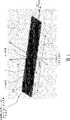
图1是示出了第一优选实施方式中的极小标签及其天线的结构的立体图。图中示出的标签1的尺寸是宽53mm、纵深7mm。FIG. 1 is a perspective view showing the structure of a very small tag and its antenna in the first preferred embodiment. The size of the
标签1在一个平面上包括:由导体形成的双极天线2、馈电部3和电感部4。优选的是,将Cu、Au或Al用作上述导体。The
馈电部3在双极天线2的中心构造芯片安装部。在芯片安装部中,安装IC芯片5。在馈电部3的两侧形成1mm宽的双极部6。以这种方式来构造整个双极天线2。The
通过在至少四个弯曲部(bending part)(7-1、7-2、7-3和7-4)处向内弯曲的矩形旋涡(rectangular eddy)的形状来分别形成双极天线2的双极(包括设置在两侧的双极部6)。即,在该优选实施方式中双极部6分别具有四个弯曲部。The dipoles of the
当四个弯曲部7分别直线展开时的双极天线2的全长被形成为比该天线的谐振波长的一半短。The overall length of the
此外,在双极部6与6(其以矩形旋涡的形状形成)之间在双极天线2的中心附近设置上述电感部4。Further, the above-described
电感部4相对于双极天线2的馈电部3(即,IC芯片5)并联连接到双极部6和6。The
安装在馈电部3中的IC芯片5例如是具有500Ω的Rc和1.4pF的Cc的芯片。电感部4设置在天线侧,并取消了IC芯片5的1.4pF的电容组件。The
图1示出的实施方式中以几乎一个矩形回路的形状来形成上述电感部4。电感部4的回路形状并不限于这种形状,而可以是正方形、圆形或与这些回路类似的形状。In the embodiment shown in FIG. 1 , the above-mentioned
分别在标签1的两个表面(图1中的顶面和底面)上覆盖介电常数εr为3且厚度t为0.75mm的树脂保护膜8。Resin
例如,将对苯二甲酸乙二酯膜(terephthalate ethylene film)等用作树脂保护膜8。对于树脂保护膜,另选的是,可以在标签1的两个表面上覆盖适合的纸张。For example, a terephthalate ethylene film or the like is used as the
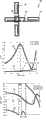
图2是示出了通过电磁场仿真器计算的、标签1的双极天线2的反射的频率特性的图。FIG. 2 is a graph showing the frequency characteristics of the reflection of the
在该图中,水平轴表示频率(800到1100MHz),而垂直轴表示反射(-5到0dB)。如从该图中所知,在975MHz附近反射最低。In this figure, the horizontal axis represents frequency (800 to 1100 MHz), and the vertical axis represents reflection (-5 to 0 dB). As can be seen from the figure, the reflection is lowest around 975 MHz.
图3是示出了通过上述电磁场仿真器计算的、标签1的双极天线2的增益值的图。FIG. 3 is a graph showing gain values of the
在该图中,水平轴表示频率(800到1100MHz),而垂直轴表示天线增益(-4到2dBi)。该图中示出的天线增益在1050MHz附近最大。In this figure, the horizontal axis represents frequency (800 to 1100 MHz), and the vertical axis represents antenna gain (-4 to 2 dBi). The antenna gain shown in this figure is maximum around 1050 MHz.
即,存在反射在1050MHz附近较高的缺点。然而,由于如图3所示,天线增益在1050MHz附近较大,所以这补偿了反射较高的缺点。That is, there is a disadvantage that reflection is high near 1050 MHz. However, since the antenna gain is larger around 1050 MHz as shown in Figure 3, this compensates for the higher reflection.
图4是示出了通过在Microsoft Excel上对标签1的双极天线2的上述反射特性和增益特性进行组合而获得的通信距离特性的图。4 is a graph showing communication distance characteristics obtained by combining the above-described reflection characteristics and gain characteristics of the
在该图中,水平轴表示频率(800到1100MHz),而垂直轴表示相对于作为参考的最大距离的通信距离。In this figure, the horizontal axis represents the frequency (800 to 1100 MHz), and the vertical axis represents the communication distance with respect to the maximum distance as a reference.
如上所述,标签1的双极天线2的通信距离特性相对于读/写器的工作频率953MHz不对称。通信距离特性在高于读/写器的工作频率953MHz的频率侧变化平缓,并且相对稳定。As described above, the communication distance characteristic of the
通过假定在图1中示出的树脂保护膜8上方和下方存在空气,来进行上述电磁场仿真器的计算。因此,在读/写器的工作频率953MHz处的通信距离是在标签1(即,双极天线2)处于空气中的情况下的距离。The calculation of the electromagnetic field simulator described above was performed by assuming the presence of air above and below the resin
空气中的通信距离是通过将图4中示出的指定最大距离乘以0.95而获得的距离。即,确保了最大距离的95%。The communication distance in the air is a distance obtained by multiplying the specified maximum distance shown in FIG. 4 by 0.95. That is, 95% of the maximum distance is ensured.
当例如将该标签1附于εr为3且厚度为2mm的塑料上时,天线周边的有效介电常数增加,而且频带偏移大约10%。即,将图4中示出的波形向低频侧偏移大约100MHz。When, for example, this
换言之,在图4的波形中频率1050MHz(其比953MHz高大约10%)处的相对通信距离的值是当将标签1附于厚度为2mm的塑料上时的通信距离。In other words, the value of the relative communication distance at a frequency of 1050 MHz (which is about 10% higher than 953 MHz) in the waveform of FIG. 4 is the communication distance when the
此时的通信距离与图4中示出的最大距离的比率是0.8,即,确保了最大距离的80%。The ratio of the communication distance at this time to the maximum distance shown in FIG. 4 is 0.8, that is, 80% of the maximum distance is secured.
如也从图4证明了的是,本优选实施方式中的标签1可以确保高达最大通信距离的80%或更大的距离,并且即使在空气中或即使附于泡沫聚苯乙烯或厚度为2mm的塑料上,标签1也具有极高的距离稳定性。As also proved from FIG. 4, the
本优选实施方式中的标签1的特征在于,将包括双极部和电感部的天线图案调整为在读/写器的工作频率953MHz附近尽可能地接近天线的最优值。The
在比953MHz高的频率处,虽然反射偏离了天线的最优值并且变得更高,但是天线增益的增加避免了通信距离特性劣化。At a frequency higher than 953 MHz, although the reflection deviates from the optimum value of the antenna and becomes higher, the increase of the antenna gain prevents the communication distance characteristic from deteriorating.
为了提高在比953MHz高的频率处的天线增益,使得天线的全长更接近于可以获得高增益效率的天线的谐振波长的一半。In order to increase the antenna gain at frequencies higher than 953 MHz, the overall length of the antenna is made closer to half the resonance wavelength of the antenna at which high gain efficiency can be obtained.
本优选实施方式中的标签1的双极天线2的天线图案的特征在于,使得当所有弯曲部7直线展开时的天线的全长稍微短于天线的谐振波长λ的一半。The antenna pattern of the
在图1中示出的实施方式中,当所有弯曲部7直线展开时的天线的全长是大约120mm,天线的谐振波长λ的一半是大约130到140mm。考虑到覆盖在顶面和底面上的树脂保护膜8,设定天线的谐振波长λ的可容许裕量10mm。In the embodiment shown in FIG. 1 , the overall length of the antenna when all the bent portions 7 are straightly developed is about 120 mm, and half of the resonance wavelength λ of the antenna is about 130 to 140 mm. The allowable margin of the resonance wavelength λ of the antenna was set at 10 mm in consideration of the resin
此外,使双极部6从端部向内弯曲,从而使这些单元尽可能地接近直线。此外,由于不希望使双极单元6与6靠近,因此优选的是,在双极单元6与6之间形成电感单元4。Furthermore, the dipoles 6 are bent inwards from the ends so that the cells are as close to straight as possible. Furthermore, since it is not desirable to bring the bipolar units 6 and 6 close together, it is preferable to form the
通过这种设置,将953MHz处的阻抗设定为接近天线的最优值的值,而且天线的增益在1050MHz附近变为最大。With this setting, the impedance at 953 MHz is set to a value close to the optimum value of the antenna, and the gain of the antenna becomes maximum around 1050 MHz.
通过这种方式,即使在空气中或即使将标签1附于泡沫聚苯乙烯或厚度为2mm的塑料上时,也可以确保具有极高的距离稳定性的标签1(其可以确保高达最大通信距离的80%或更大的距离)。In this way, a
在本实施方式中的具有宽53mm、纵深7mm的尺寸的标签1中,在双极单元6和6中的每一个中都形成四个弯曲部7,如图1所示。为了减小天线的尺寸,可以将双极单元6和6中的每一个中的弯曲部7的数量增加到五个、六个或更大的数量。In the
(第二优选实施方式)(Second preferred embodiment)
上述标签1是输出线性偏振波的标签。在第二优选实施方式中,不作修改地使用输出线性偏振波的上述标签1而不需要提供特殊电路等,而且实现了生成圆偏振波并延伸了其与读/写器的通信距离的标签。The above-mentioned
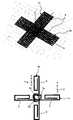
图5的上部是示出了第二优选实施方式中的生成圆偏振波的标签的结构的立体图,而图5的下部是示出了图5的上部中示出的结构的去除了树脂保护膜的俯视图。The upper part of FIG. 5 is a perspective view showing the structure of a label generating circularly polarized waves in the second preferred embodiment, and the lower part of FIG. 5 is a view showing the structure shown in the upper part of FIG. 5 with the resin protective film removed. top view.
对于图1中示出的第一优选实施方式中的标签1,其长边的右部和左部(正X方向和负X方向)相对于中心对称,但是其短边的上部和下部(正Y方向和负Y方向)相对于中心不对称。For the
通过将与图1中示出的标签类似的两个标签1(1a、1b)以直角交叉并且对它们进行层叠,来构造图5中示出的交叉双标签10。标签1a和1b的构造与图1中描述的相同。The crossed
在图5的下部中,标签1a附近的被赋予X、Y和Z的箭头表示它们的对应方向并且指定标签1a的取向。标签1b附近的箭头以类似的方式指定了标签1b的取向。In the lower part of FIG. 5 , the arrows assigned X, Y and Z in the vicinity of the
在本实施方式中,将其正Y方向被定向为另一个标签的正X方向的标签称为第一标签1a,而将其正Y方向被定向为另一个标签的负X方向的标签称为第二标签1b。In this embodiment, a label whose positive Y direction is oriented to the positive X direction of another label is called a
即,本实施方式中的交叉双标签10包括第一标签1a和第二标签1b,第一标签1a和第二标签1b以90°的角度交叉,使得电感部4(4a、4b)的回路尽可能宽地交叠。此外,将第一标签1a和第二标签1b层叠为在它们的交叠部分中尽可能紧密地接触。That is, the crossed
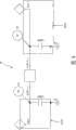
在图6中,上部示意性地示出了以交叉形状层叠的第一标签1a和第二标签1b,中部示出了例如由树脂等制成的固定件,而下部示出了由固定件11固定的第一标签1a和第二标签1b。In FIG. 6 , the upper part schematically shows the
在固定件11中,形成交叉形状的凹槽12,如图6的中部所示。将第一标签1a和第二标签1b插入交叉形状的凹槽12中,并通过合适的构件(未示出)从上方挤压并紧固。In the fixing
通过交叉并层叠第一标签1a和第二标签1b来实现的交叉双标签10的结构并不限于由其中形成有交叉形状的凹槽12的固定件11来进行固定的结构。例如,可以在两个树脂片之间密封第一标签1a和第二标签1b。The structure of the cross
在图7中,上部是示出了读/写器(R/W)的天线的偏振波的方向的示意图,中部是用于说明当第一标签1a的偏振波表面被定向在读/写器的方向上时执行的交叉双标签10的操作的示意图,而下部是用于说明当第二标签1b的偏振波表面被定向在读/写器的方向上时执行的交叉双标签10的操作的示意图。In Fig. 7, the upper part is a schematic diagram showing the direction of the polarized wave of the antenna of the reader/writer (R/W), and the middle part is for explaining when the polarized wave surface of the
如果第一标签1a的偏振波表面被定向在读/写器的方向上(如图7的中部所示),则第一标签1a进行操作。The
当第一标签1a如上所述开始进行操作时,电流流入第一标签1a的电感单元4a的回路。结果,在第一标签1a的电感单元4a的回路与第二标签1b的电感单元4b的回路之间进行高频耦合。结果,第二标签1b在其相位延迟90°的情况下进行操作,如下所述。When the
如果第二标签1b的偏振波表面被定向在读/写器的方向上(如图7的下部所示),则第二标签1b进行操作。The
当第二标签1b如上所述开始进行操作时,电流流入第二标签1b的电感单元4b的回路。结果,在第二标签1b的电感单元4b的回路与第一标签1a的电感单元4a的回路之间进行高频耦合。结果,第一标签1b在其相位延迟90°的情况下进行操作。When the
图8是示出了用于通过电磁场仿真器来计算上述交叉双标签10的操作的计算模型的示意图。FIG. 8 is a schematic diagram showing a calculation model for calculating the operation of the above-mentioned crossed
第一标签1a和第二标签1b的IC芯片5和5分别具有1.43pF的电容组件Ccp。此外,IC芯片5和5分别具有420Ω的内部阻抗Rcp。The IC chips 5 and 5 of the
图9是示出了通过电磁场仿真器进行的计算的结果的图。图9的上图示出了分别在第一标签1a和第二标签1b的IC芯片5和5中生成的电压与其周期之间的关系,而图9的下图示出了周期与分别在IC芯片5和5中生成的电压的相位之间的关系。FIG. 9 is a graph showing the results of calculations performed by an electromagnetic field simulator. The upper graph of FIG. 9 shows the relationship between the voltages generated in the IC chips 5 and 5 of the
在图9的上图中,水平轴表示从0.7到1.2GHz的电压的周期,而垂直轴表示从0到1.2V的电压。In the upper graph of FIG. 9, the horizontal axis represents the period of the voltage from 0.7 to 1.2 GHz, and the vertical axis represents the voltage from 0 to 1.2V.
如图9的上图所示,在频率为0.953GHz的周期中,在标签1a的IC芯片中生成电压V1,而在标签1b的IC芯片中生成几乎与电压V1(0.88V)相同的电压V2。As shown in the upper graph of Fig. 9, in a period with a frequency of 0.953GHz, a voltage V1 is generated in the IC chip of the
在图9的下图中,水平轴表示从0.7到1.2GHz的电压的周期,而垂直轴表示从负180°到正180°的周期的相位。In the lower graph of FIG. 9, the horizontal axis represents the period of the voltage from 0.7 to 1.2 GHz, while the vertical axis represents the phase of the period from minus 180° to plus 180°.
从图9的下图中示出的周期与相位之间的关系证明:在0.953GHz的周期处(在该周期处生成几乎与标签1a的电压V1相同的电压V2,如上图所示),标签1b的电压V2的相位相对于标签1a的电压V1的相位延迟90°。From the relationship between cycle and phase shown in the lower graph of Fig. 9, it is proved that at a cycle of 0.953 GHz (at which a voltage V2 almost identical to the voltage V1 of
即,如图9所示,在953MHz的工作频率处,与对于标签1a生成的0.88V的电压相比,在标签1b中生成0.8V的电压,而且标签1b的相位相对于标签1a的相位延迟。That is, as shown in FIG. 9, at an operating frequency of 953 MHz, a voltage of 0.8 V is generated in
即,在0.953GHz的周期处重复以延迟了90°的相位执行的上述操作。因此,证明当将标签1a和1b视为一对时,执行了与圆偏振波的操作相近的操作。That is, the above-described operation performed with a phase delayed by 90° is repeated at a cycle of 0.953 GHz. Therefore, it was proved that when the
然而,理想地,优选的是,通过在标签1a和1b中生成相同电压并通过使它们的相位偏移90°,来执行与圆偏振波的操作更接近的操作。Ideally, however, it is preferable to perform an operation closer to that of a circularly polarized wave by generating the same voltage in the
此外,此时如图7的中部所示,如果读/写器的圆偏振波的方向(图7的上部中的逆时针方向)与交叉双标签10的旋转方向相匹配,则它们的通信距离增大。In addition, as shown in the middle part of Figure 7 at this time, if the direction of the circularly polarized wave of the reader/writer (the counterclockwise direction in the upper part of Figure 7) matches the rotation direction of the crossed
即,也可以在增大为生成圆偏振波的读/写器与生成线性偏振波的标签之间的最大通信距离的√2倍(即,1.41倍)的距离内读取标签1a包含的信息。That is, it is also possible to read the information contained in the
相反,当标签1b开始进行操作时,标签1a在其相位延迟90°的情况下进行操作,如图7的下部所示,上述圆偏振波的工作方向与读/写器的圆偏振波的旋转方向相反。因此,与标签1a的情况相反,标签1b的通信距离变得较短。On the contrary, when the
然而,如果将读/写器设置为能够在预定周期处在前向方向和后向方向之间切换圆偏振波的旋转方向,则标签1a和1b都可以在增大为单个标签的距离的1.41倍的距离内进行通信。However, if the reader/writer is set up to be able to switch the direction of rotation of the circularly polarized wave between the forward direction and the backward direction at a predetermined period, both
图10是示出了当标签1a和1b不在它们的交叠部分(交叉部分)中彼此紧密接触并且具有1mm的距离h的间隙时通过电磁场仿真器进行的计算的结果的图。FIG. 10 is a graph showing the results of calculations by an electromagnetic field simulator when the
图10的上部是示出了通过以1mm的距离h的间隙使标签1a和1b交叉而实现的交叉双标签15的示意图,图10的中部是示出了分别在标签1a和1b中生成的电压与其周期之间的关系的图,图10的下部是示出了周期与分别在标签1a和1b中生成的电压的相位之间的关系的图。The upper part of Fig. 10 is a schematic diagram showing the crossed double tag 15 realized by crossing the
在图10中部的图与图9上部的图之间进行比较,在标签1b中生成的电压V2相对于在标签1a中生成的电压V1稍微减小。Comparing between the middle graph of FIG. 10 and the upper graph of FIG. 9 , the voltage V2 generated in the
也在图9下部的图与图10下部的图之间进行比较,证明在标签1a中生成的电压V1与在标签1b中生成的电压V2之间的相位差是75°。即,圆偏振波稍微变形(deform)。A comparison is also made between the lower graph of Fig. 9 and the lower graph of Fig. 10, demonstrating that the phase difference between the voltage V1 generated in the
根据上述结果,优选的是,使得标签1a和1b在交叉部分中尽可能紧密地接触,以在交叉双标签中生成圆偏振波。From the above results, it is preferable to bring the
也证明了当这些标签没有紧密接触地交叉而是以预定间隙交叉时生成了椭圆偏振波。It was also demonstrated that elliptically polarized waves were generated when these tags crossed not in close contact but with a predetermined gap.
图11是示出了当标签1a和1b的电感部4a和4b的回路完全不交叠时通过电磁场仿真器进行的计算的结果的图。FIG. 11 is a graph showing the results of calculations performed by an electromagnetic field simulator when the loops of the
图11上部的示意图示出了通过使得电感部的回路完全不交叠来交叉标签1a和1b而实现的交叉双标签17。图11中部的图示出了分别在标签1a和1b中生成的电压与其周期之间的关系。图11下部的图示出了周期与分别在标签1a和1b中生成的电压的相位之间的关系。The upper schematic diagram of Fig. 11 shows a crossed double tag 17 achieved by crossing
从图11中部的图证明:与在标签1a中生成的电压V1相比,几乎没有生成标签1b的电压V2,即,在这些标签之间没有进行谐振耦合。It is proved from the graph in the middle of FIG. 11 that the voltage V2 of the
因此,优选的是,使得标签1a和1b的电感单元的回路尽可能宽地交叠。因此,优选的是,电感单元的回路采用正方形、圆形或它们的类似形状。Therefore, it is preferable to have the loops of the inductive units of the
上述优选实施方式针对UHF频带中的RFID系统。然而,本发明自然也可应用于2.45GHz的RFID系统。The preferred embodiments described above are directed to RFID systems in the UHF band. However, the invention is naturally also applicable to RFID systems at 2.45 GHz.
此外,上述优选实施方式针对读/写器侧生成圆偏振波的情况。然而,如果读/写器侧生成处于线性偏振波与圆偏振波之间的椭圆偏振波,则可以通过以例如60°的角度而不是以90°的角度交叉并层叠这两个标签,来使交叉双标签侧以椭圆偏振波进行操作。In addition, the above-described preferred embodiments are directed to the case where circularly polarized waves are generated on the reader/writer side. However, if the reader/writer side generates elliptically polarized waves between linearly polarized waves and circularly polarized waves, it is possible to make The crossed double label side operates with elliptically polarized waves.
另选的是,可以通过彼此偏移电感部的回路来使交叉双标签以椭圆偏振波进行操作。Alternatively, the crossed ditags can be made to operate with elliptically polarized waves by offsetting the loops of the inductive parts from each other.
如上所述,优选的是,电感部的回路采用正方形、圆形或它们的类似形状。然而,如果回路采用矩形,则标签可以执行与圆偏振波的操作足够接近的操作。因此,只要两个标签分别具有回路,则交叉双标签和使用该交叉双标签的RFID系统自然也可以适用于这两个标签。As described above, it is preferable that the loop of the inductance part adopts a square, circular or similar shape. However, if the loop takes a rectangular shape, the tag can perform an operation close enough to that of a circularly polarized wave. Therefore, as long as the two tags have loops respectively, the crossed double tag and the RFID system using the crossed double tag can naturally also be applied to these two tags.
(第三实施方式)(third embodiment)
这里描述用于实际使用交叉双标签的环境。The environment for actually using crossed double labels is described here.
当大量生产标签时,在正常情况下分别将不同的ID写入这些标签。相应地,在使用根据本发明而构造的交叉双标签的情况下,当读/写器在短距离内与交叉双标签进行通信时,读/写器读取标签1a和1b的两个ID。When labels are mass-produced, it is normal to write different IDs to these labels respectively. Accordingly, in the case of using the cross dual tag constructed according to the present invention, when the reader/writer communicates with the cross dual tag within a short distance, the reader/writer reads two IDs of the
因此,优选的是,当假定标签1a是读/写器侧希望读取的标签时,则通过将标签1b指定为虚设(dummy)并且在读/写器内将标签1b的ID预先指定为“清除(kill)”,来使得读/写器只读取标签1a的信息。Therefore, it is preferable that, when it is assumed that the
这是基于在工厂发货时分别将不同ID写入所有标签的假设。然而,存在设置有用户存储器(其中信息可自由地写入IC芯片内的区域)的多种标签类型。This is based on the assumption that different IDs are individually written to all tags at the time of factory shipment. However, there are various tag types provided with user memory (an area in which information can be freely written within the IC chip).
在这种情况下,将相同信息写入标签1a和1b的用户区域,即使当读/写器在短距离内读取标签1b时,也可以避免出现问题。In this case, writing the same information into the user area of
此外,如从图7中明显得到的,在相反的方向上切换读/写器的圆偏振波表面,由此可以延伸标签1b的通信距离,并且可以缩短标签1a的通信距离。Furthermore, as is apparent from FIG. 7, the circularly polarized wave surface of the reader/writer is switched in the opposite direction, whereby the communication distance of the
如上所述,读/写器可以通过在前向方向和后向方向之间切换读/写器的圆偏振波表面,来在经延伸的通信距离内读取标签1a和1b的信息。即,可以使读/写器读取分别被写入到两个用户存储器的不同信息,由此避免浪费用户存储器。As described above, the reader/writer can read the information of the
传统上,为了实现这些标签的圆偏振波,必须交叉生成线性偏振波的两个标签,并且必须设置诸如90°移相器的复杂电路,如上所述。然而,通过根据本发明的交叉双标签,可以只通过交叉并层叠现有标签(其生成线性偏振波并分别具有电感部的回路),来延伸与读/写器的通信距离。Conventionally, in order to realize circularly polarized waves of these tags, two tags generating linearly polarized waves had to be crossed, and a complicated circuit such as a 90° phase shifter had to be provided, as described above. However, with the interleaved double tag according to the present invention, it is possible to extend the communication distance with the reader/writer only by intersecting and laminating existing tags which generate linearly polarized waves and respectively have loops of inductance parts.
Claims (9)
Translated fromChineseApplications Claiming Priority (2)
| Application Number | Priority Date | Filing Date | Title |
|---|---|---|---|
| JP2007-125055 | 2007-05-09 | ||
| JP2007125055AJP4806373B2 (en) | 2007-05-09 | 2007-05-09 | Tag device and RFID system using the same |
Publications (2)
| Publication Number | Publication Date |
|---|---|
| CN101303747Atrue CN101303747A (en) | 2008-11-12 |
| CN101303747B CN101303747B (en) | 2011-05-18 |
Family
ID=39713718
Family Applications (1)
| Application Number | Title | Priority Date | Filing Date |
|---|---|---|---|
| CN2008100964232AExpired - Fee RelatedCN101303747B (en) | 2007-05-09 | 2008-05-09 | Crossed double tags and RFID systems using crossed double tags |
Country Status (6)
| Country | Link |
|---|---|
| US (1) | US8022886B2 (en) |
| EP (1) | EP1993168B1 (en) |
| JP (1) | JP4806373B2 (en) |
| KR (1) | KR100984429B1 (en) |
| CN (1) | CN101303747B (en) |
| TW (1) | TWI350613B (en) |
Cited By (12)
| Publication number | Priority date | Publication date | Assignee | Title |
|---|---|---|---|---|
| CN101925152A (en)* | 2009-06-16 | 2010-12-22 | 英特尔公司 | Context-based limitation of mobile device operation |
| CN102682255A (en)* | 2011-02-02 | 2012-09-19 | Nxp股份有限公司 | Coordinating multiple contactless data carriers |
| US8776177B2 (en) | 2009-06-16 | 2014-07-08 | Intel Corporation | Dynamic content preference and behavior sharing between computing devices |
| US8803868B2 (en) | 2009-06-16 | 2014-08-12 | Intel Corporation | Power conservation for mobile device displays |
| US9092069B2 (en) | 2009-06-16 | 2015-07-28 | Intel Corporation | Customizable and predictive dictionary |
| TWI502812B (en)* | 2012-07-24 | 2015-10-01 | Univ Nat Kaohsiung Marine | Dual polarized antenna |
| CN106295781A (en)* | 2016-09-22 | 2017-01-04 | 南京信息工程大学 | A kind of RFID label tag and People incontinence monitor system based on RFID label tag |
| CN106887687A (en)* | 2017-03-25 | 2017-06-23 | 韶关学院 | Supermarket's commodity electronic labeling Symmetric Orthogonal folding line element antenna and its application method |
| CN107392293A (en)* | 2017-06-09 | 2017-11-24 | 国网浙江省电力公司宁波供电公司 | Pipeline inspection label based on RFID |
| CN108958063A (en)* | 2018-11-02 | 2018-12-07 | 常州普纳电子科技有限公司 | A kind of intelligent household management system |
| CN110233327A (en)* | 2019-05-28 | 2019-09-13 | 北京星网锐捷网络技术有限公司 | A kind of UHF RFID reader antenna and switching method |
| CN110852412A (en)* | 2019-12-02 | 2020-02-28 | 智坤(浙江)半导体有限公司 | Ultrahigh frequency RFID tag and production and assembly method thereof |
Families Citing this family (22)
| Publication number | Priority date | Publication date | Assignee | Title |
|---|---|---|---|---|
| USD589828S1 (en)* | 2007-01-15 | 2009-04-07 | Murata Manufacturing Co., Ltd. | IC tag inlet |
| KR100978271B1 (en)* | 2008-04-01 | 2010-08-26 | 엘에스산전 주식회사 | RFID tag using built-in antenna and RFID system using same |
| JP5163506B2 (en)* | 2009-01-14 | 2013-03-13 | 三菱電機株式会社 | Animal ear tag RFID tag |
| US20100207831A1 (en)* | 2009-02-18 | 2010-08-19 | Wu Huei-Chi | Loop Dipole Antenna Module |
| JP5263365B2 (en)* | 2011-10-12 | 2013-08-14 | カシオ計算機株式会社 | Multi-frequency circularly polarized antenna |
| WO2013096995A1 (en)* | 2011-12-29 | 2013-07-04 | Ps&D Pty Ltd | Improvements in rfid tags |
| JP5609962B2 (en)* | 2012-12-10 | 2014-10-22 | 三菱電機株式会社 | Animal ear tag RFID tag |
| KR101494148B1 (en) | 2013-05-14 | 2015-02-23 | 임은석 | Parallel antenna and tag with the parallel antenna |
| USD698684S1 (en)* | 2013-06-28 | 2014-02-04 | Checkpoints Systems, Inc. | Security tag |
| JP6079520B2 (en)* | 2013-09-12 | 2017-02-15 | 凸版印刷株式会社 | Non-contact IC label |
| JP6106138B2 (en)* | 2014-09-02 | 2017-03-29 | 東芝テック株式会社 | Radiated radio wave detector |
| GB2532727A (en)* | 2014-11-25 | 2016-06-01 | Huang Yi | A compact multiband circular-polarization cross-dipole antenna |
| JP6477310B2 (en)* | 2015-07-09 | 2019-03-06 | 株式会社オートネットワーク技術研究所 | Clamp and electric wire with clamp |
| DE102015117712A1 (en) | 2015-10-16 | 2017-04-20 | Friedrich-Alexander-Universität Erlangen-Nürnberg | Imaging polarimetry |
| DE102016213330A1 (en) | 2016-07-21 | 2018-03-08 | Friedrich-Alexander-Universität Erlangen-Nürnberg | Method for locating a mobile object and transponder for this purpose |
| CN106816697B (en)* | 2016-12-26 | 2020-02-21 | 上海交通大学 | Low Profile UHF Broadband Circularly Polarized Handheld Terminal Antenna |
| JP7123641B2 (en) | 2018-06-07 | 2022-08-23 | 株式会社東芝 | chip antenna |
| GB201902620D0 (en)* | 2019-02-27 | 2019-04-10 | Secr Defence | Dual polarised planar antenna, base station and method of manufacture |
| KR102529052B1 (en)* | 2019-06-12 | 2023-05-03 | 삼성전기주식회사 | Antenna apparatus |
| SE543837C2 (en)* | 2019-12-16 | 2021-08-10 | Stora Enso Oyj | RFID tag arrangement with omnidirectional antenna characteristics |
| JP7437284B2 (en) | 2020-10-26 | 2024-02-22 | 株式会社京三製作所 | ground child |
| KR102671648B1 (en) | 2022-10-24 | 2024-06-03 | 한국철도기술연구원 | Wheel Tread Profile Structure for Railway-Vehicle |
Family Cites Families (20)
| Publication number | Priority date | Publication date | Assignee | Title |
|---|---|---|---|---|
| JPH0865225A (en)* | 1994-08-25 | 1996-03-08 | Matsushita Electric Works Ltd | Polarization diversity antenna system |
| JP3643488B2 (en) | 1998-10-30 | 2005-04-27 | 株式会社日立製作所 | IC card |
| US6720930B2 (en)* | 2001-01-16 | 2004-04-13 | Digital Angel Corporation | Omnidirectional RFID antenna |
| JP2002280829A (en)* | 2001-03-21 | 2002-09-27 | Ee C Ii Tec Kk | Antenna device |
| JP2003249871A (en)* | 2002-02-22 | 2003-09-05 | Sharp Corp | Wireless communication system |
| JP2003249820A (en) | 2002-02-22 | 2003-09-05 | Sharp Corp | Wireless communication device |
| JP2004013427A (en) | 2002-06-05 | 2004-01-15 | Toshiba Corp | Wireless card |
| JP3924512B2 (en)* | 2002-06-27 | 2007-06-06 | 株式会社東海理化電機製作所 | Chip multi-axis antenna |
| JP2004172906A (en)* | 2002-11-19 | 2004-06-17 | Fujitsu Ten Ltd | Planar antenna |
| US7042413B2 (en)* | 2003-08-22 | 2006-05-09 | Checkpoint Systems, Inc. | Security tag with three dimensional antenna array made from flat stock |
| WO2006011187A1 (en)* | 2004-07-23 | 2006-02-02 | Mitsubishi Denki Kabushiki Kaisha | Radio tag communication system |
| US7574732B2 (en)* | 2004-09-29 | 2009-08-11 | Symbol Technologies Inc | Object location based security using RFID |
| JP2006113869A (en)* | 2004-10-15 | 2006-04-27 | Mighty Card Kk | Information reading system, questioner and method for setting information reading system |
| KR100641636B1 (en)* | 2004-12-08 | 2006-11-02 | 한국전자통신연구원 | Dual Polarization Antenna and Radio Frequency Identification Reader |
| US7714794B2 (en)* | 2005-01-19 | 2010-05-11 | Behzad Tavassoli Hozouri | RFID antenna |
| JP4330575B2 (en)* | 2005-03-17 | 2009-09-16 | 富士通株式会社 | Tag antenna |
| JP2006285594A (en)* | 2005-03-31 | 2006-10-19 | Jr East Mechatronics Co Ltd | IC card |
| JP4500214B2 (en) | 2005-05-30 | 2010-07-14 | 株式会社日立製作所 | Wireless IC tag and method of manufacturing wireless IC tag |
| JP4794974B2 (en)* | 2005-10-19 | 2011-10-19 | 富士通株式会社 | Tag antenna, tag using the antenna, and RFID system. |
| JP2007295395A (en)* | 2006-04-26 | 2007-11-08 | Fujitsu Ltd | Tag antenna and tag using the same |
- 2007
- 2007-05-09JPJP2007125055Apatent/JP4806373B2/ennot_activeExpired - Fee Related
- 2008
- 2008-04-09TWTW097112843Apatent/TWI350613B/ennot_activeIP Right Cessation
- 2008-04-15USUS12/081,344patent/US8022886B2/ennot_activeExpired - Fee Related
- 2008-04-21EPEP08103626.1Apatent/EP1993168B1/ennot_activeCeased
- 2008-05-07KRKR1020080042351Apatent/KR100984429B1/ennot_activeExpired - Fee Related
- 2008-05-09CNCN2008100964232Apatent/CN101303747B/ennot_activeExpired - Fee Related
Cited By (17)
| Publication number | Priority date | Publication date | Assignee | Title |
|---|---|---|---|---|
| US9092069B2 (en) | 2009-06-16 | 2015-07-28 | Intel Corporation | Customizable and predictive dictionary |
| TWI555374B (en)* | 2009-06-16 | 2016-10-21 | 英特爾公司 | Context-based limitation of mobile device operation |
| US8776177B2 (en) | 2009-06-16 | 2014-07-08 | Intel Corporation | Dynamic content preference and behavior sharing between computing devices |
| US8803868B2 (en) | 2009-06-16 | 2014-08-12 | Intel Corporation | Power conservation for mobile device displays |
| CN101925152A (en)* | 2009-06-16 | 2010-12-22 | 英特尔公司 | Context-based limitation of mobile device operation |
| CN102682255B (en)* | 2011-02-02 | 2014-09-03 | Nxp股份有限公司 | Coordinating multiple contactless data carriers |
| US8886119B2 (en) | 2011-02-02 | 2014-11-11 | Nxp B.V. | Coordinating multiple contactless data carriers |
| CN102682255A (en)* | 2011-02-02 | 2012-09-19 | Nxp股份有限公司 | Coordinating multiple contactless data carriers |
| TWI502812B (en)* | 2012-07-24 | 2015-10-01 | Univ Nat Kaohsiung Marine | Dual polarized antenna |
| CN106295781A (en)* | 2016-09-22 | 2017-01-04 | 南京信息工程大学 | A kind of RFID label tag and People incontinence monitor system based on RFID label tag |
| CN106887687A (en)* | 2017-03-25 | 2017-06-23 | 韶关学院 | Supermarket's commodity electronic labeling Symmetric Orthogonal folding line element antenna and its application method |
| CN107392293A (en)* | 2017-06-09 | 2017-11-24 | 国网浙江省电力公司宁波供电公司 | Pipeline inspection label based on RFID |
| CN107392293B (en)* | 2017-06-09 | 2024-02-13 | 国网浙江省电力公司宁波供电公司 | RFID-based pipeline inspection tags |
| CN108958063A (en)* | 2018-11-02 | 2018-12-07 | 常州普纳电子科技有限公司 | A kind of intelligent household management system |
| CN108958063B (en)* | 2018-11-02 | 2019-01-29 | 常州普纳电子科技有限公司 | A kind of intelligent household management system |
| CN110233327A (en)* | 2019-05-28 | 2019-09-13 | 北京星网锐捷网络技术有限公司 | A kind of UHF RFID reader antenna and switching method |
| CN110852412A (en)* | 2019-12-02 | 2020-02-28 | 智坤(浙江)半导体有限公司 | Ultrahigh frequency RFID tag and production and assembly method thereof |
Also Published As
| Publication number | Publication date |
|---|---|
| KR100984429B1 (en) | 2010-09-30 |
| EP1993168B1 (en) | 2013-11-13 |
| TW200849715A (en) | 2008-12-16 |
| KR20080099799A (en) | 2008-11-13 |
| US20080291106A1 (en) | 2008-11-27 |
| US8022886B2 (en) | 2011-09-20 |
| CN101303747B (en) | 2011-05-18 |
| EP1993168A3 (en) | 2009-06-24 |
| JP2008283404A (en) | 2008-11-20 |
| EP1993168A2 (en) | 2008-11-19 |
| TWI350613B (en) | 2011-10-11 |
| JP4806373B2 (en) | 2011-11-02 |
Similar Documents
| Publication | Publication Date | Title |
|---|---|---|
| CN101303747A (en) | Crossed double tags and RFID systems using crossed double tags | |
| US11087197B2 (en) | Attention tag for retail article and retail article having same attached thereto | |
| JP4286813B2 (en) | Antenna and RFID tag equipped with the same | |
| US7954722B2 (en) | IC tag and inlet for IC tag | |
| US7876227B2 (en) | Polarization insensitive antenna for handheld radio frequency identification readers | |
| JP4794974B2 (en) | Tag antenna, tag using the antenna, and RFID system. | |
| JP6590122B1 (en) | RFID tag and article to which RFID tag is attached | |
| EP2742466B1 (en) | Improving coupling in and to rfid smart cards | |
| JP2001101371A (en) | IC card | |
| US8899489B2 (en) | Resonant circuit structure and RF tag having same | |
| JP6566558B2 (en) | Electronic device and design method thereof | |
| JP2022029374A (en) | How to place RF-tagged articles and RF-tagged articles | |
| WO2012163293A1 (en) | Super-miniaturized passive anti-metal rfid tag | |
| US9460379B2 (en) | RF tag with resonant circuit structure | |
| US10938087B2 (en) | Antenna structure for a radio frequency identification (RFID) reader, method of manufacturing thereof, RFID reader and RFID system | |
| JP2007073015A (en) | Non-contact ic tag inlet, non-contact ic tag, and antenna |
Legal Events
| Date | Code | Title | Description |
|---|---|---|---|
| C06 | Publication | ||
| PB01 | Publication | ||
| C10 | Entry into substantive examination | ||
| SE01 | Entry into force of request for substantive examination | ||
| C14 | Grant of patent or utility model | ||
| GR01 | Patent grant | ||
| CF01 | Termination of patent right due to non-payment of annual fee | ||
| CF01 | Termination of patent right due to non-payment of annual fee | Granted publication date:20110518 Termination date:20180509 |