CN101300677B - Electrically programmable fuse and method of making same - Google Patents
Electrically programmable fuse and method of making sameDownload PDFInfo
- Publication number
- CN101300677B CN101300677BCN2006800408796ACN200680040879ACN101300677BCN 101300677 BCN101300677 BCN 101300677BCN 2006800408796 ACN2006800408796 ACN 2006800408796ACN 200680040879 ACN200680040879 ACN 200680040879ACN 101300677 BCN101300677 BCN 101300677B
- Authority
- CN
- China
- Prior art keywords
- doped region
- layer
- diode
- heavily doped
- exemplary
- Prior art date
- Legal status (The legal status is an assumption and is not a legal conclusion. Google has not performed a legal analysis and makes no representation as to the accuracy of the status listed.)
- Expired - Fee Related
Links
Images


Classifications
- H—ELECTRICITY
- H01—ELECTRIC ELEMENTS
- H01L—SEMICONDUCTOR DEVICES NOT COVERED BY CLASS H10
- H01L23/00—Details of semiconductor or other solid state devices
- H01L23/58—Structural electrical arrangements for semiconductor devices not otherwise provided for, e.g. in combination with batteries
- H01L23/62—Protection against overvoltage, e.g. fuses, shunts
- H—ELECTRICITY
- H01—ELECTRIC ELEMENTS
- H01L—SEMICONDUCTOR DEVICES NOT COVERED BY CLASS H10
- H01L23/00—Details of semiconductor or other solid state devices
- H01L23/52—Arrangements for conducting electric current within the device in operation from one component to another, i.e. interconnections, e.g. wires, lead frames
- H01L23/522—Arrangements for conducting electric current within the device in operation from one component to another, i.e. interconnections, e.g. wires, lead frames including external interconnections consisting of a multilayer structure of conductive and insulating layers inseparably formed on the semiconductor body
- H01L23/525—Arrangements for conducting electric current within the device in operation from one component to another, i.e. interconnections, e.g. wires, lead frames including external interconnections consisting of a multilayer structure of conductive and insulating layers inseparably formed on the semiconductor body with adaptable interconnections
- H01L23/5252—Arrangements for conducting electric current within the device in operation from one component to another, i.e. interconnections, e.g. wires, lead frames including external interconnections consisting of a multilayer structure of conductive and insulating layers inseparably formed on the semiconductor body with adaptable interconnections comprising anti-fuses, i.e. connections having their state changed from non-conductive to conductive
- H—ELECTRICITY
- H01—ELECTRIC ELEMENTS
- H01L—SEMICONDUCTOR DEVICES NOT COVERED BY CLASS H10
- H01L23/00—Details of semiconductor or other solid state devices
- H01L23/52—Arrangements for conducting electric current within the device in operation from one component to another, i.e. interconnections, e.g. wires, lead frames
- H01L23/522—Arrangements for conducting electric current within the device in operation from one component to another, i.e. interconnections, e.g. wires, lead frames including external interconnections consisting of a multilayer structure of conductive and insulating layers inseparably formed on the semiconductor body
- H01L23/525—Arrangements for conducting electric current within the device in operation from one component to another, i.e. interconnections, e.g. wires, lead frames including external interconnections consisting of a multilayer structure of conductive and insulating layers inseparably formed on the semiconductor body with adaptable interconnections
- H—ELECTRICITY
- H01—ELECTRIC ELEMENTS
- H01L—SEMICONDUCTOR DEVICES NOT COVERED BY CLASS H10
- H01L2924/00—Indexing scheme for arrangements or methods for connecting or disconnecting semiconductor or solid-state bodies as covered by H01L24/00
- H01L2924/0001—Technical content checked by a classifier
- H01L2924/0002—Not covered by any one of groups H01L24/00, H01L24/00 and H01L2224/00
Landscapes
- Physics & Mathematics (AREA)
- Condensed Matter Physics & Semiconductors (AREA)
- General Physics & Mathematics (AREA)
- Engineering & Computer Science (AREA)
- Computer Hardware Design (AREA)
- Microelectronics & Electronic Packaging (AREA)
- Power Engineering (AREA)
- Design And Manufacture Of Integrated Circuits (AREA)
- Semiconductor Memories (AREA)
- Internal Circuitry In Semiconductor Integrated Circuit Devices (AREA)
- Electrodes Of Semiconductors (AREA)
- Connections Effected By Soldering, Adhesion, Or Permanent Deformation (AREA)
- Semiconductor Integrated Circuits (AREA)
Abstract
Description
Translated fromChinese技术领域technical field
本发明通常涉及半导体器件制造,更具体地涉及电可编程熔丝(eFuse)及其制造方法。The present invention relates generally to semiconductor device fabrication, and more particularly to electrically programmable fuses (eFuses) and methods of fabrication thereof.
背景技术Background technique
传统的eFuse可以包括多晶硅层上的起电阻的作用的硅化物。为了编程传统eFuse,可以在从传统eFuse的阴极至阳极的第一方向上驱动电流(例如通过一或多个晶体管)。通过eFuse的第一方向的驱动电流在硅化物层中形成间隙,由此暴露部分多晶硅层。被编程的eFuse的状态可以通过试图在从阳极至阴极的第二方向上驱动电流而被感知。通过其驱动电流的路径的电阻取决于编程期间在硅化物层中形成的间隙的长度。由于晶体管的工作参数和/或用于编程这样的传统eFuse的电平的控制的变化,在这样的eFuse中形成的对应的硅化物层的间隙的长度可以变化。因此,这样的传统eFuse的电阻变化。因此,希望改善的或间隙不改变的eFuse及其制造方法。Conventional eFuses may include silicide on a polysilicon layer that acts as a resistor. To program a conventional eFuse, current may be driven in a first direction from the cathode to the anode of the conventional eFuse (eg, through one or more transistors). Driving current in the first direction through the eFuse forms a gap in the silicide layer, thereby exposing a portion of the polysilicon layer. The state of a programmed eFuse can be sensed by attempting to drive current in a second direction from anode to cathode. The resistance of the path through which current is driven depends on the length of the gap formed in the silicide layer during programming. Due to variations in the operating parameters of the transistors and/or the control of the levels used to program such conventional eFuses, the length of the gaps of the corresponding silicide layers formed in such eFuses may vary. Therefore, the resistance of such a conventional eFuse varies. Accordingly, improved or unchanged clearance eFuses and methods of making the same are desired.
发明内容Contents of the invention
在本发明的第一方面中,提供了第一设备。第一设备是电可编程熔丝,其包括衬底的绝缘氧化物层上方的半导体层;在半导体层中形成的二极管,二极管包括具有第一极性的第一重掺杂区、具有第二、相反极性的第二重掺杂区和第一和第二重掺杂区之间的轻掺杂区;电可编程熔丝还包括形成于二极管上的硅化物层。In a first aspect of the invention, a first device is provided. The first device is an electrically programmable fuse comprising a semiconductor layer over an insulating oxide layer of a substrate; a diode formed in the semiconductor layer, the diode comprising a first heavily doped region having a first polarity, having a second , a second heavily doped region of opposite polarity and a lightly doped region between the first and second heavily doped regions; the electric programmable fuse further includes a silicide layer formed on the diode.
在本发明的第二方面中,提供了制造eFuse的方法。所述方法包括的步骤是:提供包括绝缘氧化物层和绝缘氧化物层上方的半导体层的衬底;在半导体层中形成二极管;并且在二极管上方形成硅化物层,其中在半导体层中形成二极管的步骤包括的步骤是:在半导体层中形成具有第一极性的第一重掺杂区;在半导体层中形成具有第二、相反极性的第二重掺杂区;并且在半导体层中第一和第二重掺杂区之间形成轻掺杂区。In a second aspect of the invention, a method of manufacturing an eFuse is provided. The method includes the steps of: providing a substrate comprising an insulating oxide layer and a semiconductor layer over the insulating oxide layer; forming a diode in the semiconductor layer; and forming a silicide layer over the diode, wherein the diode is formed in the semiconductor layer The step comprises the steps of: forming a first heavily doped region having a first polarity in the semiconductor layer; forming a second heavily doped region having a second, opposite polarity in the semiconductor layer; and forming in the semiconductor layer A lightly doped region is formed between the first and second heavily doped regions.
从下列详细描述、所附权利要求和附图,本发明的其它特征和方面将变得更为显见。Other features and aspects of the present invention will become more apparent from the following detailed description, appended claims and accompanying drawings.
附图说明Description of drawings
图1示出了根据本发明实施例的第一典型eFuse的第一典型制造方法的步骤的截面侧视图,其中多晶硅(或单晶硅层)在衬底上被构图。FIG. 1 shows a cross-sectional side view of the steps of a first exemplary manufacturing method of a first exemplary eFuse according to an embodiment of the present invention, wherein polysilicon (or single crystal silicon layer) is patterned on a substrate.
图2示出了根据本发明实施例的第一典型eFuse的第一典型制造方法的步骤的截面侧视图,其中杂质原子被注入部分的多晶硅层从而形成N+区。2 shows a cross-sectional side view of the steps of a first typical manufacturing method of a first typical eFuse according to an embodiment of the present invention, wherein impurity atoms are implanted into a part of the polysilicon layer to form an N+ region.
图3示出了根据本发明实施例的第一典型eFuse的第一典型制造方法的步骤的截面侧视图,其中杂质原子被注入部分的多晶硅层从而形成P+区和P-区。3 shows a cross-sectional side view of the steps of a first typical manufacturing method of a first typical eFuse according to an embodiment of the present invention, wherein impurity atoms are implanted into a portion of the polysilicon layer to form P+ and P- regions.
图4示出了根据本发明实施例的第一典型eFuse的第一典型制造方法的步骤的截面侧视图,其中所述衬底进行了退火。4 illustrates a cross-sectional side view of steps in a first exemplary manufacturing method of a first exemplary eFuse, wherein the substrate is annealed, according to an embodiment of the present invention.
图5示出了根据本发明实施例的第一典型eFuse的第一典型制造方法的步骤的截面侧视图,其中隔离体和分流硅化物层形成于衬底上。5 illustrates a cross-sectional side view of steps in a first exemplary fabrication method of a first exemplary eFuse in which spacers and shunt silicide layers are formed on a substrate in accordance with an embodiment of the present invention.
图6示出了根据本发明实施例的第一典型eFuse的第一典型制造方法的步骤的截面侧视图,其中层间介电质、通路和布线形成于衬底上。6 is a cross-sectional side view illustrating steps of a first exemplary manufacturing method of a first exemplary eFuse according to an embodiment of the present invention, wherein interlayer dielectrics, vias, and wiring are formed on a substrate.
图7示出了根据本发明实施例的图6的第一典型eFuse编程之后的截面侧视图。7 illustrates a cross-sectional side view of the first exemplary eFuse of FIG. 6 after programming, according to an embodiment of the present invention.
图8示出了根据本发明实施例的编程之后的图7的第一典型eFuse的多晶硅层上方的阴极和阳极的俯视图。8 illustrates a top view of the cathode and anode over the polysilicon layer of the first exemplary eFuse of FIG. 7 after programming in accordance with an embodiment of the present invention.
图9示出了根据本发明实施例的第二典型eFuse的截面侧视图。Figure 9 shows a cross-sectional side view of a second exemplary eFuse according to an embodiment of the present invention.
图10示出了根据本发明实施例的编程之后的图9的第二典型eFuse的截面侧视图。10 shows a cross-sectional side view of the second exemplary eFuse of FIG. 9 after programming according to an embodiment of the present invention.
图11示出了根据本发明实施例的编程之后的图10的第二典型eFuse的SOI层上方的阴极和阳极的俯视图。11 shows a top view of the cathode and anode above the SOI layer of the second exemplary eFuse of FIG. 10 after programming according to an embodiment of the present invention.
图12示出了根据本发明实施例的第一典型eFuse的第二典型制造方法的步骤的截面侧视图,其中氮化物层形成于衬底的构图的多晶硅层上。12 illustrates a cross-sectional side view of steps in a second exemplary fabrication method of a first exemplary eFuse in which a nitride layer is formed on a patterned polysilicon layer of a substrate in accordance with an embodiment of the present invention.
图13示出了根据本发明实施例的第一典型eFuse的第二典型制造方法的步骤的截面侧视图,其中杂质原子被注入部分多晶硅层从而形成N+区。13 shows a cross-sectional side view of the steps of the second exemplary manufacturing method of the first exemplary eFuse according to an embodiment of the present invention, wherein impurity atoms are implanted into a part of the polysilicon layer to form an N+ region.
图14示出了根据本发明实施例的第一典型eFuse的第二典型制造方法的步骤的截面侧视图,其中一或多个氧化物隔离体形成于衬底上。14 illustrates a cross-sectional side view of steps in a second exemplary fabrication method of a first exemplary eFuse in which one or more oxide spacers are formed on a substrate in accordance with an embodiment of the present invention.
图15示出了根据本发明实施例的第一典型eFuse的第二典型制造方法的步骤的截面侧视图,其中多晶硅或抗蚀剂层形成于衬底上。15 illustrates a cross-sectional side view of steps in a second exemplary method of manufacturing a first exemplary eFuse in which a polysilicon or resist layer is formed on a substrate, according to an embodiment of the present invention.
图16示出了根据本发明实施例的第一典型eFuse的第二典型制造方法的步骤的截面侧视图,其中氧化物从衬底被蚀刻并且杂质原子被注入部分多晶硅层从而形成P+区和P-区。16 shows a cross-sectional side view of steps in a second exemplary fabrication method of a first exemplary eFuse according to an embodiment of the present invention, wherein oxide is etched from the substrate and impurity atoms are implanted into part of the polysilicon layer to form P+ regions and P -district.
图17示出了第一典型eFuse的第二典型制造方法的步骤的截面侧视图,其中在多晶硅或抗蚀剂层、一或多个氧化物隔离体和氮化物层从衬底被去除之后,衬底进行了退火。17 illustrates a cross-sectional side view of steps in a second exemplary method of manufacturing a first exemplary eFuse, where after the polysilicon or resist layer, one or more oxide spacers, and nitride layers are removed from the substrate, The substrate was annealed.
图18示出了根据本发明实施例的第一典型eFuse的第二典型制造方法的步骤的截面侧视图,其中隔离体和分流硅化物层形成于衬底上。18 illustrates a cross-sectional side view of steps in a second exemplary fabrication method of a first exemplary eFuse in which spacers and shunt silicide layers are formed on a substrate in accordance with an embodiment of the present invention.
图19示出了根据本发明实施例的第一典型eFuse的第三典型制造方法的步骤的截面侧视图,其中一或多个氮化物隔离体形成于衬底上。19 illustrates a cross-sectional side view of steps in a third exemplary fabrication method of a first exemplary eFuse in which one or more nitride spacers are formed on a substrate in accordance with an embodiment of the present invention.
图20示出了根据本发明实施例的第一典型eFuse的第三典型制造方法的步骤的截面侧视图,其中多晶硅或抗蚀剂层形成于衬底上。20 illustrates a cross-sectional side view of steps in a third exemplary method of manufacturing a first exemplary eFuse in which a polysilicon or resist layer is formed on a substrate in accordance with an embodiment of the present invention.
图21示出了根据本发明实施例的第一典型eFuse的第三典型制造方法的步骤的截面侧视图,其中氧化物从衬底被蚀刻并且杂质原子被注入部分的多晶硅层从而形成P+区。21 shows a cross-sectional side view of steps in a third exemplary fabrication method of a first exemplary eFuse according to an embodiment of the present invention, wherein oxide is etched from the substrate and impurity atoms are implanted into a portion of the polysilicon layer to form a P+ region.
图22示出了根据本发明实施例的第一典型eFuse的第三典型制造方法的步骤的截面侧视图,其中氮化物从衬底被蚀刻并且杂质原子注入部分的多晶硅层从而形成P-区。22 illustrates a cross-sectional side view of steps in a third exemplary fabrication method of a first exemplary eFuse in which nitride is etched from the substrate and impurity atoms are implanted into a portion of the polysilicon layer to form a P-region, according to an embodiment of the present invention.
具体实施方式Detailed ways
本发明提供了改善的eFuse及其制造方法。更具体地,本发明提供了具有独立于编程期间在eFuse的硅化物层中形成的间隙的长度的电阻,并且提供了这样的eFuse的制造方法。所述eFuse包括在硅化物下面的二极管元件。在一些实施例中,二极管元件可以包括多晶硅、绝缘体上单晶硅、或其它合适的半导体材料。二极管元件在读期间被反向偏置,并且因此当感知了编程的eFuse的状态时提供了高电阻。所得的eFuse的电阻取决于二极管的形成并且变得独立于编程期间在硅化物层中形成的间隙的长度。反向二极管IV的特性界定了比包围二极管部分的单掺杂的多晶硅线长度的大小高几个量级的电阻。因此,eFuse二极管电阻既是高度可重复的也独立于硅化物间隙长度。因此,根据本发明实施例制造的eFuse的电阻可以不变化(例如,与传统单掺杂半导体eFuse一样大)。用这种方式,本发明提供了改善的eFuse及其制造方法。The present invention provides improved eFuses and methods of making the same. More specifically, the present invention provides a resistance having a length independent of a gap formed in a silicide layer of an eFuse during programming, and a method of manufacturing such an eFuse. The eFuse includes a diode element under the silicide. In some embodiments, the diode element may comprise polysilicon, silicon-on-insulator, or other suitable semiconductor materials. The diode element is reverse biased during read and thus provides a high resistance when the state of the programmed eFuse is sensed. The resulting resistance of the eFuse depends on the formation of the diode and becomes independent of the length of the gap formed in the silicide layer during programming. The characteristics of the reverse diode IV define a resistance several orders of magnitude higher than the magnitude of the length of the mono-doped polysilicon line surrounding the diode portion. Therefore, eFuse diode resistance is both highly repeatable and independent of silicide gap length. Therefore, the resistance of eFuses fabricated according to embodiments of the present invention may not change (eg, as large as conventional single-doped semiconductor eFuses). In this manner, the present invention provides improved eFuses and methods of making them.
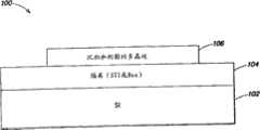
图1示出了根据本发明实施例的第一典型eFuse的第一典型制造方法的步骤的截面侧视图,其中多晶硅或单晶硅层构图于衬底上。参考图1,第一典型eFuse(图6中的600)可以由包括硅层102(例如体衬底)的衬底100制造。衬底100可以包括形成于硅层102上的绝缘氧化物层104,和形成于绝缘氧化物层上的多晶硅(例如栅极导体多晶硅)或其它合适的半导体材料的层106。以这种方式,绝缘氧化物层104可以是埋藏氧化物(BOX)层或浅沟槽隔离(STI)氧化物层。可以采用化学气相沉积(CVD)或其它合适的方法形成衬底100上的多晶硅层106。此后,可以采用反应离子蚀刻(RIE)或其它合适的方法选择性地去除部分多晶硅层106,由此构图多晶硅。如下所述,后续的衬底工艺将多晶硅层形成入第一典型eFuse的一或多个部分。1 shows a cross-sectional side view of steps in a first exemplary method of manufacturing a first exemplary eFuse, wherein a polysilicon or monocrystalline silicon layer is patterned on a substrate, according to an embodiment of the present invention. Referring to FIG. 1, a first exemplary eFuse (600 in FIG. 6) may be fabricated from a
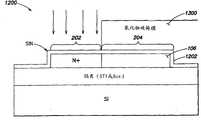
图2示出了根据本发明实施例的第一典型eFuse的第一典型制造方法的步骤的截面侧视图,其中杂质原子被注入部分的多晶硅层从而形成N+区。参考图2,可以采用旋涂技术或其它合适的方法从而在衬底100上沉积光致抗蚀剂层。可以采用使用抗蚀剂和合适的掩模的光刻或其它合适的方法构图光致抗蚀剂层成为第一掩模(例如遮挡掩模)200。以这种方式,多晶硅层106的第一部202的顶表面可以被暴露并且在掩模200下面的多晶硅层106的第二部204的顶表面可以不被暴露。2 shows a cross-sectional side view of the steps of a first typical manufacturing method of a first typical eFuse according to an embodiment of the present invention, wherein impurity atoms are implanted into a part of the polysilicon layer to form an N+ region. Referring to FIG. 2 , a photoresist layer may be deposited on the
可以采用注入工艺(例如独特或标准逻辑注入工艺)或其它合适的方法将N+杂质原子等(例如掺杂剂)注入多晶硅层106。更具体地,注入(例如逻辑N+多晶硅和扩散注入)可以在多晶硅层106的被暴露的部分(例如第一部分202)中形成具有第一极性的第一高掺杂区(例如N+掺杂区)。但是,在注入期间,掩模200可以避免杂质原子到达多晶硅层106的第二部204,由此保护第二部204。此外,在注入期间掩模200可以包含一或多个MOSFET栅极。一旦N+掺杂区形成,光致抗蚀剂剥离剂浴或其它合适的方法可以用于从衬底100剥离第一掩模200。N+ impurity atoms, etc. (eg, dopants) can be implanted into the
图3示出了根据本发明实施例的第一典型eFuse的第一典型制造方法的步骤的截面侧视图,其中杂质原子被注入部分的多晶硅层从而形成P+区和P-区。参考图3,可以采用旋涂技术或其它合适的方法从而在衬底100上沉积光致抗蚀剂层。可以采用使用抗蚀剂和合适的掩模的光刻或其它合适的方法构图光致抗蚀剂层成为第二掩模(例如遮挡掩模)(未示出)。可以定位第二掩模使得第二掩模保护多晶硅层106的第一部202并且不保护(例如暴露)多晶硅层106的第二部204。以这种方式,第二掩模可以是第一掩模200的反转。3 shows a cross-sectional side view of the steps of a first typical manufacturing method of a first typical eFuse according to an embodiment of the present invention, wherein impurity atoms are implanted into a portion of the polysilicon layer to form P+ and P- regions. Referring to FIG. 3 , a photoresist layer may be deposited on the
可以采用注入工艺或其它合适的方法将P+杂质原子等(例如掺杂剂)注入多晶硅层106。更具体地,注入(例如逻辑P+多晶硅和扩散注入)可以在多晶硅层106的被暴露的部分(例如第二部204)中形成具有第二相反极性的第二高掺杂区(例如P+掺杂区)。但是,在注入期间第二掩模可以避免杂质原子到达多晶硅层106的第一部202。一旦P+掺杂区形成,则可以使用光致抗蚀剂剥离剂浴或其它合适的方法以便从衬底100剥离第二掩模。P+ impurity atoms (such as dopants) can be implanted into the
第三掩模300可以用与相似于形成第一和第二掩模的方式形成。更具体地,可以采用旋涂技术或其它合适的方法在衬底100上沉积光致抗蚀剂层。可以采用使用抗蚀剂和合适的掩模的光刻或其它合适的方法构图光致抗蚀剂层成为第三掩模(例如遮挡掩模)。可以定位第三掩模300使得第三掩模300保护多晶硅层106的第一部202的第一子部分302并且不保护(例如暴露)多晶硅层106的第一部202的第二子部304和第二部204。以这种方式,第三掩模300可以是第一掩模200的反转的偏移版(例如具有+X sigma的第一掩模200)。可以采用注入工艺或其它合适的方法将P+杂质原子等(例如掺杂剂)注入多晶硅层106。第三掩模300允许其中注入N+杂质原子时被暴露的多晶硅层区交叠其中P+原子注入时被暴露的多晶硅区。可以选择杂质原子剂量使得多晶硅层106的第二部204的掺杂不受影响或受到轻微的影响。以这种方式,注入(例如逻辑P+多晶硅和扩散注入)可以形成轻掺杂区,例如在多晶硅层106的被暴露的部分(例如第一部202的第二子部304)中的P-掺杂区(例如P-至P+转变的梯度区)。第三掩模300可以避免在注入期间杂质原子到达多晶硅层106的第一子部302,由此保护第一子部302。一旦P-掺杂区形成,则可以采用光致抗蚀剂剥离剂浴或其它合适的方法从衬底100剥离第三掩模300。The
作为替代,可以不使用掩模形成衬底100的P-区。例如,从衬底100剥离第二掩模200之后,可以采用注入工艺或其它合适的方法将P+杂质原子等(例如掺杂剂)注入多晶硅层106。尽管多晶硅层106的第一部202的第一子部302和第二部204(和第二子部304一起)在注入期间被暴露,但是可以选择杂质原子剂量使得第一子部302和第二部206不受影响或受到轻微的影响。以这种方式,注入(例如逻辑P+多晶硅和扩散注入)可以形成多晶硅层106的第一部202的第二子部304中的P-掺杂区。Alternatively, the P-region of the
图4示出了根据本发明实施例的第一典型eFuse的第一典型制造方法的步骤的截面侧视图,其中衬底进行了退火。参考图4,衬底100可以在大约900℃至大约1100℃的温度下根据希望的掺杂区的横向梯度(例如P-至P+的转变)进行大约10秒至大约30分钟的退火。但是,可以采用较大或较小和/或不同的温度范围。此外,衬底100可以进行较长或较短时间的退火。退火的高温可以激活注入的掺杂剂N+掺杂剂、P+掺杂剂、P-掺杂剂,由此使得这样的掺杂剂可以扩散至整个对应的掺杂区302、204、304。在退火一或多个注入区期间,例如P-区可以扩展。以这种方式,具有第一子区302耦合至第二子区304的N+P-结的二极管400可以形成于多晶硅层106中。4 illustrates a cross-sectional side view of steps in a first exemplary manufacturing method of a first exemplary eFuse, wherein the substrate is annealed, according to an embodiment of the present invention. Referring to FIG. 4 , the
图5示出了根据本发明实施例的第一典型eFuse的第一典型制造方法的步骤的截面侧视图,其中硅化物层和隔离体形成于衬底上。参考图5,可以使用CVD或其它合适的方法沉积(例如共形地)分流硅化物层或其它合适的材料于衬底100上。此后,可以采用RIE或其它合适的方法去除部分这样的硅化物层(例如选择性地对于多晶硅)。以这种方式,硅化物层500可以形成于多晶硅层106上。如下所述,硅化物层500可以起第一典型eFuse(图6中的600)的熔丝元件的作用。在一些实施例中,硅化物层500可以是大约300埃至大约800埃的厚度(尽管可以采用较大或较小和/或不同的厚度范围)。硅化物层500可以在栅极导体硅化期间形成于多晶硅层106上。作为替代,硅化物层500可以作为独立的工艺步骤而形成。例如,如果希望多晶硅层106上方较浅的硅化物层,可以使用CVD或其它合适的方法以及随后的RIE或其它合适的方法从而在栅极导体硅化期间在多晶硅层106上形成绝缘材料层。此后,较浅的硅化物层可以用上述方式形成于多晶硅层106上。5 illustrates a cross-sectional side view of steps in a first exemplary manufacturing method of a first exemplary eFuse in which a silicide layer and spacers are formed on a substrate in accordance with an embodiment of the present invention. Referring to FIG. 5 , a shunt suicide layer or other suitable material may be deposited (eg, conformally) on the
可以采用CVD或其它方法沉积(例如共形地)氧化物层(例如氧化硅)或其它合适的绝缘材料(例如氮化硅)于衬底100上。此后,可以使用RIE或其它合适的方式以便选择性地对于硅化物去除部分这样的氧化物层。以这种方式,一或多个氧化物隔离体502可以形成于对应的多晶硅层106的侧壁504(例如垂直侧壁)和/或对应的硅化物层500的侧壁506上。An oxide layer (eg, silicon oxide) or other suitable insulating material (eg, silicon nitride) may be deposited (eg, conformally) on the
在一些实施例中,形成一或多个氧化物隔离体502之前,可以采用CVD或其它方法沉积(例如共形地)薄遮挡层于衬底100上。形成一或多个氧化物隔离体时,遮挡层可以起保护绝缘氧化物层104的作用。In some embodiments, prior to forming one or more oxide spacers 502, a thin masking layer may be deposited (eg, conformally) on the
衬底100可以进行退火从而激活硅化物层500中的硅化物。此外,在一些实施例中,硅化物层500和/或氧化物隔离体502形成时,可以形成制造于衬底100上的一或多个MOSFET(例如标准NMOS和/或PMOS晶体管)的源极和漏极注入区(尽管这样的注入区可以形成得较早或较晚)。The
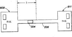
图6示出了根据本发明实施例的第一典型eFuse的第一典型制造方法的步骤的截面侧视图,其中层间介电质、通路和布线形成于衬底上。参考图6,层间介电质可以沉积或形成于衬底100上。例如,后端(back end of lineBEOL)绝缘氧化物层602或其它合适的材料可以形成于衬底100上使得BEOL绝缘氧化物层602围绕eFuse 600的多晶硅和硅化物层106、500。接触开口或通路可以形成于BEOL绝缘氧化物层602中。接触604可以分别形成于这样的通路中。此外,一或多层布线606可以形成于衬底100上。例如,eFuse 600的第一布线608(例如第一端子)可以耦合至二极管400的区,例如起阴极609作用的第一子区302,并且eFuse 600的第二布线610(例如第二端子)可以耦合至二极管400的区,例如起阳极611作用的第二部204。形成层间介电质、通路和布线的方法是本领域技术人员所知道的。因此,这样的方法不在此详细描述。以这种方式,可以形成第一典型eFuse 600。更具体地,包括起熔丝元件作用的浅硅化物层500的eFuse 600可以形成于横向多晶硅二极管400上。6 is a cross-sectional side view illustrating steps of a first exemplary manufacturing method of a first exemplary eFuse according to an embodiment of the present invention, wherein interlayer dielectrics, vias, and wiring are formed on a substrate. Referring to FIG. 6 , an interlayer dielectric may be deposited or formed on the
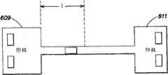
图7示出了根据本发明实施例的编程之后的图6的第一典型eFuse 600的截面侧视图并且图8示出了根据本发明实施例的编程之后的图7的第一典型eFuse 600的多晶硅层106上方的阴极609和阳极611的俯视图。参考图7和8,第一典型eFuse 600可以通过相对于阳极611负地偏置阴极609而被编程。例如,比二极管400的阳极611更负的电压可以施加至阴极609。因此,在硅化物层500中的电子可以从阴极609流至阳极611。这样的电子流(例如硅化物电子迁移)可以导致间隙700形成于硅化物层500中。例如,硅化物层500可以首先接近对于阴极的接触打开并且向阳极611进展。可以选择多晶硅层500中横向np结的位置(例如N+区耦合至P-区之处),使得pn结在eFuse编程期间总是不被覆盖(例如被暴露)。间隙700可以具有大约0.4μm至大约0.9μm的长度l(尽管可以采用较大或较小和/或不同的长度范围)。间隙长度可以是用于施加迁移硅化物的功率的函数。7 shows a cross-sectional side view of the first
因此,编程之后,在eFuse 600中驱动的电流(例如在阴极609和阳极611之间)可以通过在多晶硅层106中形成的二极管400。编程之后,例如,在读出期间(例如读操作),阴极609可以对于阳极611被正地偏置。例如,比二极管400的阳极611更正的电压可以施加至阴极609。因此,二极管400被反向偏置。穿过eFuse 600的电流可以被限制为反向偏置的二极管400的漏电流。更具体地,穿过eFuse 600的电流可以独立于跨过eFuse 600所施加的电压。当被反向偏置时,二极管400的结构可以进行阻挡动作,由此提供高度可重复的预定电阻(例如根据二极管结构的电阻)。因此,在读出期间,在eFuse 600被编程使得暴露二极管400的N+P-结的间隙700形成于硅化物层500中,eFuse 600可以提供高度可重复的电流(例如根据二极管结构的电流)。以这种方式,在读出期间的电阻和流过eFuse的电流可以独立于在eFuse编程期间形成的硅化物电子迁移间隙长度l。与此相反,传统eFuse可以包括小于在编程期间形成的硅化物电子迁移间隙的电阻。因此,在读出期间这样的eFuse的电阻和通过的电流取决于间隙1的长度。Thus, after programming, current driven in eFuse 600 (eg, between
通过使用第一典型eFuse 600的第一典型制造方法,可以以读出期间高度可重复的电阻和电流制造多个eFuse 600。eFuse 600可以分别包括横向多晶硅二极管上方的硅化物熔丝元件。By using the first exemplary fabrication method of the first
图9示出了根据本发明实施例的第二典型eFuse的截面侧视图。参考图9,第二典型eFuse 900可以相似于第一典型eFuse 600。但是,与第一典型eFuse600相比,第二典型eFuse 900可以包括形成于衬底906的绝缘体上硅(SOI)层904中的二极管元件(例如二极管902)。更具体地,衬底906可以包括绝缘氧化物(例如埋藏氧化物(BOX))层908上方的单晶硅层904。但是,二极管元件可以形成于其它合适的材料中。第二典型eFuse 900可以包括起熔丝元件作用的形成于SOI层904上的硅化物层910。Figure 9 shows a cross-sectional side view of a second exemplary eFuse according to an embodiment of the present invention. Referring to FIG. 9, the second
与第一典型eFuse 600相比,在第二典型eFuse 900的单晶硅中,注入的掺杂剂的横向扩散可以比在第一典型eFuse 600的多晶硅中低。较低的扩散率(例如较低的扩散性)对于某些应用可以是希望的(例如根据工艺集成的考虑)。The lateral diffusion of implanted dopants may be lower in the monocrystalline silicon of the second
第二典型eFuse 900可以使用相似于制造第一典型eFuse 600的第一典型方法的第一典型方法制造。但是,与制造第一eFuse 600的第一典型方法相比,制造第二eFuse 900的第一典型方法由包括硅层(例如体衬底)、形成于硅层上的绝缘氧化物层908(例如埋藏氧化物(BOX))、和形成于绝缘氧化物层908上的SOI层904(例如单晶硅层)或其它合适的材料的层的衬底906形成第二典型eFuse 900。第二典型eFuse 900的第一典型制造方法可以构图SOI层904并且在这样构图的SOI层904中形成eFuse902的部分(例如二极管元件)。衬底906的处理可以相似于在图1-6中示出的第一典型eFuse600的第一典型制造方法的步骤,但是在下列方面可以不同。构图起包括有源硅(例如RX层)区作用的SOI层904之后,并且在栅极工艺之前,以相似于在图2和3中所示出的第一典型eFuse 600的第一典型制造方法的步骤,使N+和P+注入进入对应的SOI层904的区。在这样的注入期间,在衬底906上制造的一或多个MOSFET的区可以受到由构图的光致抗蚀剂层形成的遮挡掩模保护。The second
此后,可以进行对于MOSFET的正常的栅极工艺。例如,这样的栅极工艺可以包括栅极导体的沉积和构图、延伸、晕注入、隔离体形成、和源极和漏极注入。在栅极工艺期间,SOI层注入区可以受到通过一或多个遮挡掩模构图的光致抗蚀剂层保护。此后,所有的栅极导体材料可以从SOI层904的注入区蚀刻掉,并且可以采用CVD或其它合适的方法形成SOI层904上的硅化物层910。作为替代,硅化物层910可以在不同的时间形成。例如,如果希望SOI层904上方较浅的硅化物层,则可以采用CVD或其它合适的方法之后的RIE或其它合适的方法,从而在栅极导体硅化期间在SOI层904上形成绝缘材料层。此后,较浅的硅化物层可以用上述方式形成于SOI层904上。Thereafter, normal gate processes for MOSFETs can be performed. For example, such gate processes may include deposition and patterning of gate conductors, extensions, halo implants, spacer formation, and source and drain implants. During the gate process, the SOI layer implanted regions may be protected by a photoresist layer patterned through one or more block masks. Thereafter, all gate conductor material can be etched away from the implanted regions of the
图10示出了根据本发明实施例的编程之后的图9的第二典型eFuse的截面侧视图并且图11示出了编程之后的图10的第二典型eFuse 900的SOI层904上方的阴极609和阳极611的俯视图。参考图10-11,相似于第一典型eFuse 600,第二典型eFuse 900可以通过相对于阳极611负地偏置阳极609而编程。例如,比二极管902的阳极611更负的电压施加至阴极609。因此,硅化物层910中的电子可以从阴极609流至阳极611。这样的电子流(例如硅化物电子迁移)可以导致间隙700形成于硅化物层500中。例如,硅化物层500可以首先靠近阴极609的接触打开并且向阳极611进展。可以选择SOI层904中的横向N+P-结的位置,使得N+P-结永远不被覆盖(例如在eFuse编程期间被暴露)。间隙700可以具有大约0.4μm至大约0.9μm的长度1(尽管可以采用较大或较小和/或不同的长度范围)10 shows a cross-sectional side view of the second exemplary eFuse of FIG. 9 after programming and FIG. 11 shows the
结果,编程之后,在eFuse 900中被驱动的电流(例如在阴极609和阳极611之间)可以通过在SOI层904中形成的二极管902。编程之后,例如,在读出期间(例如读操作),阴极609可以相对于阳极611被正地偏置。例如,比二极管902的阳极611更正的电压可以施加至阴极609。因此,二极管902被反向偏置。通过eFuse 900的电流可以限制为反向偏置的二极管900的漏电流。更具体地,通过eFuse 900的电流可以独立于跨过eFuse 900所施加的电压。当被反向偏置时,二极管902的结构可以进行阻挡动作,由此提供高度可重复的预定电阻(例如根据二极管结构的电阻)。因此,在读出期间,在eFuse 900被编程使得暴露二极管902的N+P-结的间隙700形成于硅化物层910中,eFuse 900可以提供高度可重复的电流(例如根据二极管结构的电流)。以这种方式,在读出期间的电阻和通过eFuse 900的电流可以独立于在eFuse编程期间形成的硅化物电子迁移间隙长度1。As a result, current driven in eFuse 900 (eg, between
通过使用第一典型eFuse 900的第一典型制造方法,可以以读出期间高度可重复的电阻和电流制造多个eFuse 900。eFuse 900可以分别包括横向SOI二极管上方的硅化物熔丝元件。By using the first exemplary fabrication method of the first
尽管上面描述了第一典型eFuse 600的第一典型制造方法,但是本发明提供了制造这样的eFuse 600的另外的方法。该另外的方法通过使得附加的注入区(例如第二注入区)与多晶硅层106中先前形成的第一注入区对齐,可以改善第一典型方法。以这种方式,第二注入区可以使其自身对准至第一注入区。用这种方式对齐多晶硅层106的注入区使得可以制造具有读出期间的高重复性的反向偏置漏电流的多个eFuse 900。例如,图12示出了根据本发明实施例的第一典型eFuse 600的第二典型制造方法的步骤的截面侧视图,其中氮化物层形成于衬底的构图的多晶硅层上。参考图12,第一典型eFuse600的第二典型制造方法可以相似于图1的构图的衬底100而处理构图的衬底1200。可以采用CVD或其它合适的方法沉积(例如共形地)氮化物层1202或其它合适的材料于衬底1200上。氮化物层1202可以是大约5nm至大约100nm厚(尽管可以采用较大或较小和/或不同的厚度范围)。Although a first exemplary method of manufacturing a first
图13示出了根据本发明实施例的第一典型eFuse的第二典型制造方法的步骤的截面侧视图,其中杂质原子注入部分多晶硅层106从而形成N+区。参考图13,可以采用CVD或其它合适的方法在衬底1200上形成氧化物层。氧化物层可以是大约50nm至大约500nm厚(尽管可以采用较大或较小和/或不同的厚度范围)。可以采用化学机械平坦化(CMP)或其它合适的方法平坦化氧化物层。可以采用RIE或其它合适的方法去除部分氧化物层,由此形成第一掩模(例如氧化物硬掩模)1300。氧化物掩模1300的厚度取决于沉积的氧化物层的厚度。以这种方式,多晶硅层106的第一部202的顶表面可以被暴露并且在掩模1300下面的多晶硅层106的第二部204的顶表面可以不被暴露。13 shows a cross-sectional side view of the steps of the second exemplary manufacturing method of the first exemplary eFuse according to an embodiment of the present invention, in which impurity atoms are implanted into a portion of the
可以采用注入工艺或其它合适的方法注入N+杂质原子等(例如掺杂剂)通过氮化物层1202进入多晶硅层106。更具体地,注入(例如逻辑N+多晶硅和扩散注入)可以形成第一高掺杂区,例如多晶硅层106的被暴露的部分(例如第一部202)中的N+掺杂区。但是,掩模1300可以避免杂质原子在注入期间到达多晶硅层106的第二部204,由此保护了第二部204。N+ impurity atoms (such as dopants) can be implanted into the
图14示出了根据本发明实施例的第一典型eFuse的第二典型制造方法的步骤的截面侧视图,其中一或多个氧化物隔离体形成于衬底上。参考图14,可以采用CVD或其它合适的方法沉积(例如共形地)氧化物层(例如氧化硅)于衬底1200上。此后,可以采用RIE或其它合适的方法去除一或多个部分氧化物层,由此形成一或多个氧化物隔离体1400(或其它合适的材料的隔离体)。例如,氧化物隔离体1400可以形成于氧化物掩模1300的被暴露的侧壁1402和氮化物层1202的被暴露的侧壁1404上。一或多个氧化物隔离体1400的厚度可以取决于沉积的氧化物层的厚度。氧化物隔离体1400的厚度可以确定N+掺杂区的边缘和随后通过杂质原子注入形成的例如P+掺杂区的第二高掺杂区之间的距离。更具体地,氧化物隔离体1400的宽度可以确定随后在N+掺杂区和P+掺杂区之间形成的例如P-掺杂区的轻掺杂区的宽度。因而,沉积的氧化物层的厚度,并且因此,氧化物隔离体1400可以起用于确定随后在第一典型eFuse 600的第二典型制造方法期间形成的二极管的特性的设计变量的作用。结果,制造eFuse 600时所采用的氧化物隔离体的厚度可以被改变从而分别精细地调整制造的eFuse 600的二极管特性。14 illustrates a cross-sectional side view of steps in a second exemplary fabrication method of a first exemplary eFuse in which one or more oxide spacers are formed on a substrate in accordance with an embodiment of the present invention. Referring to FIG. 14 , an oxide layer (eg, silicon oxide) may be deposited (eg, conformally) on a
图15示出了根据本发明实施例的第一典型eFuse的第二典型制造方法的步骤的截面侧视图,其中多晶硅或抗蚀剂层形成于衬底上。参考图15,多晶硅、光致抗蚀剂、或其它合适的材料(例如其它聚合物)的层1500、可以形成于衬底1200上。例如可以采用CVD或其它合适的方法沉积多晶硅层于衬底1200上。作为替代,可以采用旋涂技术或其它合适的方法沉积光致抗蚀剂层于衬底1200上。此后,可以采用CMP或其它合适的方法平坦化多晶硅或光致抗蚀剂层1500。多晶硅或光致抗蚀剂层1500可以被平坦化,使得多晶硅层106上方的氧化物隔离体1400的顶部和氧化物掩模1300可以被消耗。结果,这样的氧化物隔离体1400的顶部可以是平坦的。15 illustrates a cross-sectional side view of steps in a second exemplary method of manufacturing a first exemplary eFuse in which a polysilicon or resist layer is formed on a substrate, according to an embodiment of the present invention. Referring to FIG. 15 , a
图16示出了根据本发明实施例的第一典型eFuse的第二典型制造方法的步骤的截面侧视图,其中氧化物从衬底被蚀刻并且杂质原子被注入部分多晶硅层从而形成P+区和P-区。参考图16,可以采用蚀刻或其它合适的方法从衬底1200去除被暴露的氧化物。可以采用例如对于多晶硅或光致抗蚀剂和氮化物有选择性的各向同性蚀刻去除被暴露的氧化物隔离体1400并且从衬底1200去除氧化物掩模1300。以这种方式,多晶硅层106的第一部202的第一子部302可以通过多晶硅或光致抗蚀剂层1500被保护(例如被覆盖)。但是,多晶硅层106的第一部202的第一子部304和第二部204可以被暴露。16 shows a cross-sectional side view of steps in a second exemplary fabrication method of a first exemplary eFuse according to an embodiment of the present invention, wherein oxide is etched from the substrate and impurity atoms are implanted into part of the polysilicon layer to form P+ regions and P -district. Referring to FIG. 16, the exposed oxide may be removed from the
可以采用注入工艺或其它合适的方法将P+杂质原子等(例如掺杂剂)注入多晶硅层106。可以选择杂质原子剂量使得注入(例如逻辑P+多晶硅和扩散注入)可以形成比如多晶硅层106的第一部202的第二子部304中的P-掺杂区的轻掺杂区和在比如多晶硅层106的第二区204中的例如P+掺杂区的高掺杂区。更具体地,P+掺杂可以补偿N+掺杂区的掺杂,由此形成P-掺杂区。以这种方式,氧化物隔离体(图14中的1400)可以界定接受N+注入和P+注入两者的多晶硅层106的区(例如重叠区),由此界定在多晶硅层106中形成的P-区的宽度。结果,氧化物隔离体1400可以界定P+掺杂区的边可以从N+掺杂区的边偏移的距离。在一些实施例中,上述P+注入可以与在衬底1200上制造MOSFET区(例如PMOS)时进行的P+注入同时进行(尽管上述P+注入可以较早或较晚进行)。P+ impurity atoms (such as dopants) can be implanted into the
图17示出了第一典型eFuse的第二典型制造方法的步骤的截面侧视图,其中从衬底去除多晶硅或抗蚀剂层、一或多个氧化物隔离体和氮化物层之后,衬底经历退火。参考图17,可以从衬底1200去除多晶硅或光致抗蚀剂层1500。例如,可以采用RIE或其它合适的方法从衬底1200去除多晶硅层。作为替代,可以采用光致抗蚀剂剥离剂浴或其它合适的方法从衬底104剥离光致抗蚀剂层。可以采用RIE或其它合适的方法从衬底1200去除一或多个氧化物隔离体1400。例如,可以去除相邻于氮化物层1202的侧壁1404的氧化物隔离体1400。用相似的方式,可以从衬底1200去除氮化物层1202。17 illustrates a cross-sectional side view of steps in a second exemplary fabrication method of a first exemplary eFuse, wherein after removal of the polysilicon or resist layer, one or more oxide spacers, and nitride layers from the substrate, the substrate undergo annealing. Referring to FIG. 17 , polysilicon or
参考图4,衬底1200可以用上述方式进行退火。退火的高温可以激活注入的掺杂剂N+掺杂剂和/或P+掺杂剂,由此使得这样的掺杂剂可以扩散至整个其中注入了掺杂剂的对应的区302、204、304。在退火一或多个注入区期间,例如P-区可以扩展。以这种方式,具有第一子部302耦合至第二部304的PN-结的二极管1700可以形成于多晶硅层106中。Referring to FIG. 4, the
图18示出了根据本发明实施例的第一典型eFuse的第二典型制造方法的步骤的截面侧视图,其中隔离体和分流硅化物层形成于衬底上。参考图18,硅化物层1800和隔离体1802可以用参考图5所述的相似的方式形成于衬底上,并且因此,在此不详细描述所述步骤。此后,层间介电质、通路和布线可以用上面参考图6所述的相似的方式形成于衬底1200上,并且因此,在此不详细描述所述步骤。18 illustrates a cross-sectional side view of steps in a second exemplary fabrication method of a first exemplary eFuse in which spacers and shunt silicide layers are formed on a substrate in accordance with an embodiment of the present invention. Referring to FIG. 18 , a
通过使用第一典型eFuse 600的第二典型制造方法,可以采用隔离体1400(例如氧化物隔离体)从而对齐在形成P+区时所采用的掩模1500和在形成N+区时所采用的掩模1300。以这种方式,隔离体1400可以使掩模1500的边可以使其自身对准于掩模1300的边,反之亦然。通过以这种方式对齐掩模1500、1300,如同所希望的,P+掺杂注入区可以相对于多晶硅层106的N+掺杂注入区而定位。By using the second exemplary fabrication method of the first
本发明还可以提供第二典型eFuse 900的第二典型制造方法。第二典型eFuse 900的第二典型制造方法可以相似于第一典型eFuse 600的第二典型制造方法。但是,与第一典型eFuse 600的第二典型制造方法相比,第二典型eFuse 900的第二典型制造方法可以由衬底形成第二典型eFuse 900,相似于图9的衬底906,所述衬底包括硅层(例如体衬底)、形成于硅层上的绝缘氧化物层908(例如埋藏氧化物(BOX)),和形成于绝缘氧化物层908上的SOI层904(例如单晶硅或其它合适材料的层)。第二典型eFuse 900的第二典型制造方法可以构图SOI层904并且在这样构图的SOI层904中形成eFuse 900的部分(例如二极管元件)。衬底906的工艺可以相似于在图10-18中示出的第一典型eFuse 600的第二典型制造方法的步骤,但是可以在下列方面中不同。构图起包括有源硅(例如RX层)的区的作用的SOI层904之后,并且在栅极工艺之前,以相似于在图12-17中所示出第二典型900的第一典型制造方法的步骤的方式,可以使N+和P+注入进入SOI层904的对应的区。在这样的注入期间,在衬底906上制造的一或多个MOSFET的区可以受到由构图的光致抗蚀剂层形成的遮挡掩模保护。The present invention can also provide a second exemplary manufacturing method of the second
此后,可以进行对于MOSFET的正常的栅极工艺。例如,这样的栅极工艺可以包括栅极导体的沉积和构图、延伸、晕注入、隔离体形成、和源极和漏极注入。在栅极工艺期间,SOI层904的注入区可以受到通过一或多个遮挡掩模构图的光致抗蚀剂层保护。此后,所有的栅极导体材料可以从SOI层904的注入区蚀刻掉,并且可以采用CVD或其它合适的方法,从而形成SOI层904上的硅化物层910。作为替代,硅化物层910可以在不同的时间形成。例如,如果希望SOI层904上方较浅的硅化物层,则可以采用CVD或其它合适的方法之后的RIE或其它合适的方法,从而在栅极导体硅化期间在SOI层904上形成绝缘材料层。此后,较浅的硅化物层可以用上述方式形成于SOI层904上。Thereafter, normal gate processes for MOSFETs can be performed. For example, such gate processes may include deposition and patterning of gate conductors, extensions, halo implants, spacer formation, and source and drain implants. During the gate process, the implanted regions of the
第二典型eFuse 900的第二典型制造方法通过使第二注入区可以与在SOI层904中先前形成的第一注入区对齐,可以改善第二典型eFuse 900的第一典型制造方法。以这种方式,第二注入区可以使其自身对准第一注入区。用这种方式对齐SOI层904的注入区使得可以制造在读出期间具有高重复性的反向偏置漏电流的多个eFuse 900。The second exemplary fabrication method of the second
此外,本发明还可以提供制造这样的eFuse 600、900的另外的方法。相似于第一典型eFuse 600的第二典型制造方法和第二典型实施例eFuse 900的第二典型制造方法,第一典型eFuse 600的第三典型制造方法和第二典型实施例eFuse 900的第三典型制造方法,分别可以使第二注入区与在多晶硅层中先前形成的第一注入区对齐。此外,这样的方法可以用于制造包括不同类型二极管(例如PIN二极管)的eFuse 600、900。Additionally, the present invention may also provide additional methods of making
第一eFuse 600的第三典型制造方法可以相似于第一eFuse 600的第二典型制造方法。例如,可以如同在图12-13中所示出的处理衬底1900。以下,图19示出了根据本发明实施例的第一典型eFuse 600的第三典型制造方法的步骤的截面侧视图,其中一或多个氮化物隔离体形成于衬底1900上。参考图19,可以采用CVD或其它合适的方法沉积(例如共形地)氮化物层(例如氮化硅)于衬底1900上。此后,可以采用RIE或其它合适的方法去除一或多个部分氮化物层,由此形成一或多个氮化物隔离体1902。例如,氮化物隔离体1902可以形成于氮化物层1202的被暴露的侧壁1402上。一或多个氮化物隔离体1902的厚度可以取决于沉积的氮化物层的厚度。氮化物隔离体1902的厚度可以确定第一高掺杂区(例如N+掺杂区)的边缘和随后通过杂质原子注入形成的第二高掺杂区(例如P+掺杂区)之间的距离。更具体地,氮化物隔离体1902的宽度可以确定随后形成于N+掺杂区和P+掺杂区之间的轻掺杂区(例如P-掺杂注入区)的宽度。沉积的氮化物层的厚度,并且因而氮化物隔离体1902的厚度,可以起用于确定在第一典型eFuse 600的第三典型制造方法过程中随后形成的二极管的特性的设计变量的作用。因此,制造eFuse 600时所采用的氮化物隔离体的厚度可以变化,从而分别精细地调整制造的eFuse 600的二极管的特性。The third exemplary method of manufacturing the
图20示出了根据本发明实施例的第一典型eFuse的第三典型制造方法的截面侧视图,其中多晶硅或抗蚀剂形成于衬底上。参考图20,多晶硅、光致抗蚀剂或其它合适材料(例如另一聚合物)的层1500可以形成于衬底1900上。例如,可以采用CVD或其它合适的方法沉积多晶硅层于衬底1900上。作为替代,可以采用旋涂技术或其它合适的方法沉积光致抗蚀剂层于衬底1900上。此后,可以采用CMP或其它合适的方法平坦化多晶硅或光致抗蚀剂层1500。可以平坦化多晶硅或光致抗蚀剂层1500,使得多晶硅层106上方的部分氮化物隔离体1902和氧化物掩模1300可以被消耗。结果,这样的氮化物隔离体1902的顶部可以是平坦的。20 illustrates a cross-sectional side view of a third exemplary fabrication method of a first exemplary eFuse in which polysilicon or resist is formed on a substrate in accordance with an embodiment of the present invention. Referring to FIG. 20 , a
图21示出了根据本发明实施例的第一典型eFuse 600的第三典型制造方法的步骤的截面侧视图,其中氧化物从衬底1900被蚀刻并且杂质原子被注入部分多晶硅层106从而形成例如P+区的轻掺杂区。参考图21,可以采用蚀刻或其它合适的方法从衬底1900去除被暴露的氧化物。例如,可以采用对于多晶硅或光致抗蚀剂和氮化物具有选择性的各向同性蚀刻从衬底1900去除被暴露的氧化物掩模1300。以这种方式,多晶硅层106的第一部202可以被多晶硅或光致抗蚀剂的层1500保护(例如被覆盖)。但是,多晶硅层106的第二部204可以被暴露。21 illustrates a cross-sectional side view of steps in a third exemplary fabrication method of a first
可以采用注入工艺或其它合适的方法注入P+杂质原子等(例如掺杂剂)进入多晶硅层106。可以选择杂质原子剂量,使得注入(例如逻辑P+多晶硅和扩散注入)可以在多晶硅层106的第二区204中形成P+掺杂区。结果,氮化物隔离体1902可以界定P+掺杂区的边可以从N+掺杂区的边偏移的距离。在一些实施例中,上述P+注入可以与形成在衬底上制造的MOSFET(例如PMOS)的区时进行的P+注入同时进行(尽管上述P+注入可以较早或较晚进行)。P+ impurity atoms (such as dopants) can be implanted into the
图22示出了根据本发明实施例的第一典型eFuse 600的第三典型制造方法的步骤的截面侧视图,其中氮化物从衬底1900被蚀刻并且杂质原子被注入部分多晶硅层106从而形成P-区。参考图22,可以采用RIE或其它合适的方法从衬底1900去除被暴露的氮化物隔离体1902。可以采用注入工艺或其它合适的方法注入杂质原子(例如掺杂剂)例如P+杂质原子进入多晶硅层106的被暴露的部分。可以对于该第三注入选择杂质原子剂量(例如定制),使得注入(例如逻辑P+多晶硅和扩散注入)可以在多晶硅层106的第一区202的第二子部304中形成P-掺杂区。结果,氮化物隔离体1902可以界定P+掺杂区的边可以从N+掺杂区的边偏移的距离,和P-区的宽度。以这种方式,根据杂质原子剂量,可以在多晶硅层106中形成N+P-、PIN或其它合适的二极管2200。22 illustrates a cross-sectional side view of steps in a third exemplary fabrication method of a first
此后,多晶硅或光致抗蚀剂的层1500,被暴露的氮化物隔离体1902和氮化物层1202可以从衬底1900被去除。衬底1900可以用相似于参考图17所示出的方式进行退火(例如激活注入的掺杂剂)。结果,这样的步骤在此不进行详细描述。此后,根据本发明实施例,用相似于参考图18所示出的方式,隔离体和硅化物层可以形成于衬底1900上。结果,这样的步骤在此不进行详细描述。此后,层间介电质、通路和布线可以用相似于上面参考图6所述的方式形成于衬底1900上,并且因此,这样的步骤在此不进行详细的描述。Thereafter, the
通过使用第一典型eFuse 600的第三典型制造方法,可以采用隔离体1902(例如氮化物隔离体)对齐形成P+区(和P-区)时所采用的掩模1500和形成N+区时所使用的掩模1300。以这种方式,隔离体1902可以使掩模1500的边其自身对准于掩模1300的边,并且反之亦然。通过用这种方式对齐掩模1500、1300,P+掺杂注入区可以如同所希望的相对于多晶硅层106的N+掺杂注入区定位。By using the third exemplary manufacturing method of the first
本发明还提供了第二典型eFuse 900的第三典型制造方法。第二典型eFuse 900的第三典型制造方法可以相似于第一典型eFuse 600的第三典型制造方法。但是,与第一典型eFuse 600的第三典型制造方法相比,第二典型eFuse 900的第三典型制造方法可以由衬底形成第二典型eFuse 900,相似于图9的衬底906,器包括硅层(例如体衬底)、形成于硅层上的绝缘氧化物层908(例如埋藏氧化物(BOX))、和形成于绝缘氧化物层908上的SOI层904(例如单晶硅或其它合适材料的层)。第二典型eFuse 900的第三典型制造方法可以构图SOI层904并且在这样构图的SOI层904中形成eFuse 900的部分(例如二极管元件)。衬底906的工艺可以相似于第一典型eFuse 600的第三典型制造方法的步骤,但是可以在下列方法中不同。构图起包括有源硅(例如RX层)区作用的SOI层904之后,并且在栅极工艺之前,以相似于第一典型eFuse 600的第三典型制造方法的对应的注入步骤,使N+和P+注入进入对应的SOI层904的区。在这样的注入期间,在衬底906上制造的一或多个MOSFET的区可以被由构图的光致抗蚀剂层形成的遮挡掩模保护。The present invention also provides a third exemplary manufacturing method of the second
此后,可以进行对于MOSFET的正常的栅极工艺。例如,这样的栅极工艺可以包括栅极导体的沉积和构图、延伸、晕注入、隔离体形成、和源极和漏极注入。在栅极工艺期间,SOI层904的注入区可以受到通过一或多个遮挡掩模构图的光致抗蚀剂层的保护。此后,所有的栅极导体材料可以从SOI层904的注入区蚀刻掉,并且可以采用CVD或其它合适的方法,从而形成SOI层904上的硅化物层910。作为替代,硅化物层910可以在不同的时间形成。例如,如果希望SOI层904上方较浅的硅化物层,则可以采用CVD或其它合适的方法之后的RIE或其它合适的方法,从而在栅极导体硅化期间在SOI层904上形成绝缘材料层。此后,较浅的硅化物层可以用上述方式形成于SOI层904上。Thereafter, normal gate processes for MOSFETs can be performed. For example, such gate processes may include deposition and patterning of gate conductors, extensions, halo implants, spacer formation, and source and drain implants. During the gate process, the implanted regions of the
第一典型eFuse 600的第三典型制造方法和第二典型eFuse 900的第三典型制造方法可以通过使第二注入区可以与在多晶硅或SOI层中先前形成的第一注入区对齐,改善eFuse 600、900的其它的典型制造方法。The third exemplary manufacturing method of the first
本发明还提供了形成典型eFuse 600、900的方法,与上述的一些方法相比,采用较大数量的注入工艺(例如三个注入工艺)。例如,这样的方法可以相似于参考图19-22的第三典型方法。但是,与之相比,氮化物隔离体1902可以在第一注入工艺从而形成高掺杂区(例如N+区)之前形成。因此,所得的第一高掺杂区可以比通过第三典型方法形成的小,因为氮化物隔离体1902可以避免第一注入到达106下面的半导体层的部分。此后,氧化物掩模1300可以被去除并且可以形成平坦化的多晶硅或光致抗蚀剂掩模1500。可以采用第二注入工艺从而形成第二高掺杂区204(例如P+区)。此后,平坦化的多晶硅或光致抗蚀剂掩模1500和氮化物隔离体1902可以被去除。此外,可以采用第三注入工艺从而在整个半导体层106的上方注入P-杂质原子等。以这种方式,第三注入工艺可以形成轻掺杂区304(例如P-区)而不影响第一和第二高掺杂区202、204。作为替代,通过不进行第三注入工艺,可以采用本方法形成PIN二极管。The present invention also provides methods of forming a
前面的描述仅公开了本发明的典型实施例。落在本发明的范围之内的上述公开的设备和方法的改进对于本领域的技术人员是显见的。例如,本发明可以提供eFuse 600、900,其包括在编程期间由于硅化物电子迁移而可以被暴露的二极管元件。随后的以反向偏置配置的编程的eFuse的读出独立于硅化物电子迁移间隙长度,因为所得的高二极管元件的电阻比与可变迁移范围相关的公差大得多。此外,如同所述,根据本发明实施例的eFuse 600、900可以包括二极管元件(例如阻挡二极管)。因此,当电流被驱动通过eFuse 600、900时,eFuse 600、900的随后复原可以被减小和/或消除。这样的电流可以独立于跨过eFuse 600、900施加的电压。在包括作为电阻的多晶硅层的传统硅化物(例如NiSi2、CoSi2、TiSi2或其它硅化物成分)eFuse中,复原或再编程可以出现(例如当eFuse被连续地读时)。但是,本方法和设备可以提供其中这样的复原被减小和/或消除的硅化物eFuse。另外,根据本发明实施例的eFuse 600、900可以用于只读存储器(ROM)用户可编程阵列,由此提供了这样的阵列的低功率解决方案。尽管上述eFuse 600、900可以包括二极管元件,该二极管元件包括N+掺杂区、P-掺杂区和P+掺杂区,但是在其它实施例中,二极管元件可以包括不同的掺杂区,例如P+掺杂区、N-掺杂区和N+掺杂区。The foregoing description discloses only typical embodiments of the present invention. Modifications of the above disclosed apparatus and methods which fall within the scope of the invention will be apparent to those skilled in the art. For example, the present invention may provide
因而,尽管结合其典型实施例公开了本发明,但是应当理解其它的实施例也落在本由所附权利要求界定的本发明的范围之内。Thus, while this invention has been disclosed in connection with exemplary embodiments thereof, it is to be understood that other embodiments are within the scope of this invention as defined by the appended claims.
Claims (13)
Translated fromChineseApplications Claiming Priority (3)
| Application Number | Priority Date | Filing Date | Title |
|---|---|---|---|
| US11/266,740US7659168B2 (en) | 2005-11-03 | 2005-11-03 | eFuse and methods of manufacturing the same |
| US11/266,740 | 2005-11-03 | ||
| PCT/EP2006/067883WO2007051765A2 (en) | 2005-11-03 | 2006-10-27 | Electrically programmable fuse |
Publications (2)
| Publication Number | Publication Date |
|---|---|
| CN101300677A CN101300677A (en) | 2008-11-05 |
| CN101300677Btrue CN101300677B (en) | 2010-05-19 |
Family
ID=37669600
Family Applications (1)
| Application Number | Title | Priority Date | Filing Date |
|---|---|---|---|
| CN2006800408796AExpired - Fee RelatedCN101300677B (en) | 2005-11-03 | 2006-10-27 | Electrically programmable fuse and method of making same |
Country Status (9)
| Country | Link |
|---|---|
| US (1) | US7659168B2 (en) |
| EP (1) | EP1946371B1 (en) |
| JP (1) | JP5226524B2 (en) |
| KR (1) | KR20080064149A (en) |
| CN (1) | CN101300677B (en) |
| AT (1) | ATE490555T1 (en) |
| DE (1) | DE602006018643D1 (en) |
| TW (1) | TWI392082B (en) |
| WO (1) | WO2007051765A2 (en) |
Families Citing this family (34)
| Publication number | Priority date | Publication date | Assignee | Title |
|---|---|---|---|---|
| JPH07110778B2 (en) | 1986-08-06 | 1995-11-29 | 株式会社ヤマウ | Sulfur plate manufacturing method |
| US7323761B2 (en)* | 2004-11-12 | 2008-01-29 | International Business Machines Corporation | Antifuse structure having an integrated heating element |
| US7320911B2 (en)* | 2004-12-06 | 2008-01-22 | Micron Technology, Inc. | Methods of forming pluralities of capacitors |
| US7851885B2 (en)* | 2007-03-07 | 2010-12-14 | International Business Machines Corporation | Methods and systems involving electrically programmable fuses |
| US8076754B2 (en)* | 2007-03-09 | 2011-12-13 | Silicon Laboratories | Silicide-interface polysilicon resistor |
| US20090045484A1 (en)* | 2007-08-16 | 2009-02-19 | International Business Machines Corporation | Methods and systems involving electrically reprogrammable fuses |
| US7759766B2 (en)* | 2007-08-22 | 2010-07-20 | International Business Machines Corporation | Electrical fuse having a thin fuselink |
| US7619295B2 (en) | 2007-10-10 | 2009-11-17 | Fairchild Semiconductor Corporation | Pinched poly fuse |
| US9058887B2 (en)* | 2007-10-30 | 2015-06-16 | International Business Machines Corporation | Reprogrammable electrical fuse |
| CN101170099B (en)* | 2007-11-30 | 2012-03-28 | 上海宏力半导体制造有限公司 | Multicrystalline silicon compounds electric fuse silk part |
| US7936582B1 (en)* | 2008-03-19 | 2011-05-03 | Xilinx, Inc. | E-fuse read circuit with dual comparators |
| US7977754B2 (en)* | 2008-07-25 | 2011-07-12 | Taiwan Semiconductor Manufacturing Company, Ltd. | Poly resistor and poly eFuse design for replacement gate technology |
| US20100059823A1 (en) | 2008-09-10 | 2010-03-11 | Taiwan Semiconductor Manufacturing Company, Ltd. | Resistive device for high-k metal gate technology and method of making |
| US8178945B2 (en)* | 2009-02-03 | 2012-05-15 | International Business Machines Corporation | Programmable PN anti-fuse |
| US8865592B2 (en)* | 2009-02-03 | 2014-10-21 | Infineon Technologies Ag | Silicided semiconductor structure and method of forming the same |
| US8519507B2 (en)* | 2009-06-29 | 2013-08-27 | International Business Machines Corporation | Electrically programmable fuse using anisometric contacts and fabrication method |
| US8890260B2 (en) | 2009-09-04 | 2014-11-18 | Taiwan Semiconductor Manufacturing Company, Ltd. | Polysilicon design for replacement gate technology |
| US8530319B2 (en) | 2010-10-14 | 2013-09-10 | International Business Machines Corporation | Vertical silicide e-fuse |
| US8542517B2 (en) | 2011-06-13 | 2013-09-24 | International Business Machines Corporation | Low voltage programmable mosfet antifuse with body contact for diffusion heating |
| KR20120139361A (en) | 2011-06-17 | 2012-12-27 | 삼성전자주식회사 | E-fuse structure and method of operating the same |
| KR101896412B1 (en)* | 2011-08-01 | 2018-09-07 | 페어차일드코리아반도체 주식회사 | Poly silicon resistor, reference voltage circuit comprising the same, and manufacturing mehtod of poly silicon resistor |
| US8816473B2 (en)* | 2012-04-05 | 2014-08-26 | International Business Machines Corporation | Planar polysilicon regions for precision resistors and electrical fuses and method of fabrication |
| US9929150B2 (en)* | 2012-08-09 | 2018-03-27 | Infineon Technologies Ag | Polysilicon diode bandgap reference |
| US9293414B2 (en) | 2013-06-26 | 2016-03-22 | Globalfoundries Inc. | Electronic fuse having a substantially uniform thermal profile |
| US9159667B2 (en) | 2013-07-26 | 2015-10-13 | Globalfoundries Inc. | Methods of forming an e-fuse for an integrated circuit product and the resulting e-fuse structure |
| CN104425446B (en)* | 2013-08-20 | 2017-12-29 | 中芯国际集成电路制造(上海)有限公司 | Electric fuse structure and its application method |
| US9780012B2 (en)* | 2013-12-12 | 2017-10-03 | Fuji Electric Co., Ltd. | Semiconductor device and method for manufacturing the same |
| CN105470238A (en)* | 2014-09-09 | 2016-04-06 | 中芯国际集成电路制造(上海)有限公司 | Electrical programmable fuse device, integrated circuit and electronic device |
| FR3063573B1 (en)* | 2017-03-01 | 2019-05-03 | Stmicroelectronics (Rousset) Sas | INTEGRATED FUSE DEVICE |
| US10510662B2 (en)* | 2017-11-07 | 2019-12-17 | Globalfoundries Inc. | Vertically oriented metal silicide containing e-fuse device and methods of making same |
| CN109244061A (en)* | 2018-09-03 | 2019-01-18 | 上海华虹宏力半导体制造有限公司 | Electrically programmable fuse structure and forming method thereof |
| KR20230045177A (en) | 2021-09-28 | 2023-04-04 | 삼성전자주식회사 | Storage device and method of operating storage device |
| CN113972190A (en)* | 2021-10-19 | 2022-01-25 | 西安微电子技术研究所 | A kind of diode and preparation method thereof |
| US20240188287A1 (en)* | 2022-12-05 | 2024-06-06 | Globalfoundries U.S. Inc. | One-time programmable fuse using pn junction over gate metal layer, and related method |
Citations (3)
| Publication number | Priority date | Publication date | Assignee | Title |
|---|---|---|---|---|
| US6410367B2 (en)* | 1999-04-16 | 2002-06-25 | Micron Technology, Inc. | Fuse for use in a semiconductor device, and semiconductor devices including the fuse |
| US6621138B1 (en)* | 2002-10-21 | 2003-09-16 | Micrel, Inc. | Zener-like trim device in polysilicon |
| CN1494145A (en)* | 2002-09-27 | 2004-05-05 | ���ǵ�����ʽ���� | Fuse device and integrated circuit device using the device |
Family Cites Families (7)
| Publication number | Priority date | Publication date | Assignee | Title |
|---|---|---|---|---|
| US5708291A (en)* | 1995-09-29 | 1998-01-13 | Intel Corporation | Silicide agglomeration fuse device |
| US6088256A (en)* | 1998-09-25 | 2000-07-11 | Stmicroelectronics, Inc. | Integrated circuit with electrically programmable fuse resistor |
| US6580156B1 (en)* | 2002-04-04 | 2003-06-17 | Broadcom Corporation | Integrated fuse with regions of different doping within the fuse neck |
| US6933591B1 (en)* | 2003-10-16 | 2005-08-23 | Altera Corporation | Electrically-programmable integrated circuit fuses and sensing circuits |
| US6956277B1 (en)* | 2004-03-23 | 2005-10-18 | Taiwan Semiconductor Manufacturing Company, Ltd. | Diode junction poly fuse |
| US7323761B2 (en)* | 2004-11-12 | 2008-01-29 | International Business Machines Corporation | Antifuse structure having an integrated heating element |
| US7382036B2 (en)* | 2005-07-29 | 2008-06-03 | International Business Machines Corporation | Doped single crystal silicon silicided eFuse |
- 2005
- 2005-11-03USUS11/266,740patent/US7659168B2/enactiveActive
- 2006
- 2006-10-27KRKR1020087010994Apatent/KR20080064149A/ennot_activeCeased
- 2006-10-27JPJP2008538343Apatent/JP5226524B2/enactiveActive
- 2006-10-27WOPCT/EP2006/067883patent/WO2007051765A2/enactiveApplication Filing
- 2006-10-27CNCN2006800408796Apatent/CN101300677B/ennot_activeExpired - Fee Related
- 2006-10-27ATAT06819175Tpatent/ATE490555T1/ennot_activeIP Right Cessation
- 2006-10-27EPEP06819175Apatent/EP1946371B1/enactiveActive
- 2006-10-27DEDE602006018643Tpatent/DE602006018643D1/enactiveActive
- 2006-11-01TWTW095140404Apatent/TWI392082B/ennot_activeIP Right Cessation
Patent Citations (3)
| Publication number | Priority date | Publication date | Assignee | Title |
|---|---|---|---|---|
| US6410367B2 (en)* | 1999-04-16 | 2002-06-25 | Micron Technology, Inc. | Fuse for use in a semiconductor device, and semiconductor devices including the fuse |
| CN1494145A (en)* | 2002-09-27 | 2004-05-05 | ���ǵ�����ʽ���� | Fuse device and integrated circuit device using the device |
| US6621138B1 (en)* | 2002-10-21 | 2003-09-16 | Micrel, Inc. | Zener-like trim device in polysilicon |
Also Published As
| Publication number | Publication date |
|---|---|
| TW200733350A (en) | 2007-09-01 |
| WO2007051765A3 (en) | 2007-06-28 |
| DE602006018643D1 (en) | 2011-01-13 |
| ATE490555T1 (en) | 2010-12-15 |
| US7659168B2 (en) | 2010-02-09 |
| WO2007051765A2 (en) | 2007-05-10 |
| EP1946371A2 (en) | 2008-07-23 |
| JP5226524B2 (en) | 2013-07-03 |
| US20070099326A1 (en) | 2007-05-03 |
| TWI392082B (en) | 2013-04-01 |
| KR20080064149A (en) | 2008-07-08 |
| EP1946371B1 (en) | 2010-12-01 |
| CN101300677A (en) | 2008-11-05 |
| JP2009515330A (en) | 2009-04-09 |
Similar Documents
| Publication | Publication Date | Title |
|---|---|---|
| CN101300677B (en) | Electrically programmable fuse and method of making same | |
| US7868386B2 (en) | Method and apparatus for semiconductor device with improved source/drain junctions | |
| US4319395A (en) | Method of making self-aligned device | |
| US7410854B2 (en) | Method of making FUSI gate and resulting structure | |
| CN100562988C (en) | Method of fabricating semiconductor-on-insulator device | |
| US8598669B2 (en) | Semiconductor device, and its manufacturing method | |
| US6096591A (en) | Method of making an IGFET and a protected resistor with reduced processing steps | |
| JP3594550B2 (en) | Method for manufacturing semiconductor device | |
| US6391750B1 (en) | Method of selectively controlling contact resistance by controlling impurity concentration and silicide thickness | |
| US7964457B2 (en) | Semiconductor integrated circuit device and a manufacturing method for the same | |
| US20090267160A1 (en) | Semiconductor device and method for manufacturing the same | |
| KR100568077B1 (en) | Manufacturing Method of Semiconductor Device | |
| KR100951205B1 (en) | Low resistance MOSSF and low resistance MOSSFT manufacturing method | |
| US8481397B2 (en) | Polysilicon resistor and E-fuse for integration with metal gate and high-k dielectric | |
| US7169676B1 (en) | Semiconductor devices and methods for forming the same including contacting gate to source | |
| US6232638B1 (en) | Semiconductor device and manufacturing method for same | |
| CN1868046B (en) | Semiconductor device and method of manufacturing such a semiconductor device | |
| US20050287756A1 (en) | Semiconductor device with resistor element and its manufacture method | |
| US6638829B1 (en) | Semiconductor structure having a metal gate electrode and elevated salicided source/drain regions and a method for manufacture | |
| US6936514B1 (en) | Semiconductor component and method | |
| EP0975021B1 (en) | Process for manufacturing an electronic device including MOS transistors with salicided junctions and non-salicided resistors | |
| US6674135B1 (en) | Semiconductor structure having elevated salicided source/drain regions and metal gate electrode on nitride/oxide dielectric | |
| US20010019162A1 (en) | Stacked semiconductor integrated circuit device and manufacturing method thereof | |
| KR100646561B1 (en) | CMOS semiconductor device and method of forming the same | |
| JPH04142749A (en) | Manufacture of semiconductor device |
Legal Events
| Date | Code | Title | Description |
|---|---|---|---|
| C06 | Publication | ||
| PB01 | Publication | ||
| C10 | Entry into substantive examination | ||
| SE01 | Entry into force of request for substantive examination | ||
| C14 | Grant of patent or utility model | ||
| GR01 | Patent grant | ||
| CF01 | Termination of patent right due to non-payment of annual fee | ||
| CF01 | Termination of patent right due to non-payment of annual fee | Granted publication date:20100519 |