CN101297236A - Display device, method for manufacturing display device, substrate, and color filter substrate - Google Patents
Display device, method for manufacturing display device, substrate, and color filter substrateDownload PDFInfo
- Publication number
- CN101297236A CN101297236ACNA200680039518XACN200680039518ACN101297236ACN 101297236 ACN101297236 ACN 101297236ACN A200680039518X ACNA200680039518X ACN A200680039518XACN 200680039518 ACN200680039518 ACN 200680039518ACN 101297236 ACN101297236 ACN 101297236A
- Authority
- CN
- China
- Prior art keywords
- substrate
- ultraviolet
- sealing material
- display device
- light
- Prior art date
- Legal status (The legal status is an assumption and is not a legal conclusion. Google has not performed a legal analysis and makes no representation as to the accuracy of the status listed.)
- Pending
Links
Images


Classifications
- G—PHYSICS
- G02—OPTICS
- G02F—OPTICAL DEVICES OR ARRANGEMENTS FOR THE CONTROL OF LIGHT BY MODIFICATION OF THE OPTICAL PROPERTIES OF THE MEDIA OF THE ELEMENTS INVOLVED THEREIN; NON-LINEAR OPTICS; FREQUENCY-CHANGING OF LIGHT; OPTICAL LOGIC ELEMENTS; OPTICAL ANALOGUE/DIGITAL CONVERTERS
- G02F1/00—Devices or arrangements for the control of the intensity, colour, phase, polarisation or direction of light arriving from an independent light source, e.g. switching, gating or modulating; Non-linear optics
- G02F1/01—Devices or arrangements for the control of the intensity, colour, phase, polarisation or direction of light arriving from an independent light source, e.g. switching, gating or modulating; Non-linear optics for the control of the intensity, phase, polarisation or colour
- G02F1/13—Devices or arrangements for the control of the intensity, colour, phase, polarisation or direction of light arriving from an independent light source, e.g. switching, gating or modulating; Non-linear optics for the control of the intensity, phase, polarisation or colour based on liquid crystals, e.g. single liquid crystal display cells
- G02F1/133—Constructional arrangements; Operation of liquid crystal cells; Circuit arrangements
- G02F1/1333—Constructional arrangements; Manufacturing methods
- G02F1/1339—Gaskets; Spacers; Sealing of cells
- G—PHYSICS
- G02—OPTICS
- G02F—OPTICAL DEVICES OR ARRANGEMENTS FOR THE CONTROL OF LIGHT BY MODIFICATION OF THE OPTICAL PROPERTIES OF THE MEDIA OF THE ELEMENTS INVOLVED THEREIN; NON-LINEAR OPTICS; FREQUENCY-CHANGING OF LIGHT; OPTICAL LOGIC ELEMENTS; OPTICAL ANALOGUE/DIGITAL CONVERTERS
- G02F1/00—Devices or arrangements for the control of the intensity, colour, phase, polarisation or direction of light arriving from an independent light source, e.g. switching, gating or modulating; Non-linear optics
- G02F1/01—Devices or arrangements for the control of the intensity, colour, phase, polarisation or direction of light arriving from an independent light source, e.g. switching, gating or modulating; Non-linear optics for the control of the intensity, phase, polarisation or colour
- G02F1/13—Devices or arrangements for the control of the intensity, colour, phase, polarisation or direction of light arriving from an independent light source, e.g. switching, gating or modulating; Non-linear optics for the control of the intensity, phase, polarisation or colour based on liquid crystals, e.g. single liquid crystal display cells
- G02F1/133—Constructional arrangements; Operation of liquid crystal cells; Circuit arrangements
- G02F1/1333—Constructional arrangements; Manufacturing methods
- G02F1/1335—Structural association of cells with optical devices, e.g. polarisers or reflectors
- G02F1/133509—Filters, e.g. light shielding masks
- G02F1/133512—Light shielding layers, e.g. black matrix
- G—PHYSICS
- G02—OPTICS
- G02F—OPTICAL DEVICES OR ARRANGEMENTS FOR THE CONTROL OF LIGHT BY MODIFICATION OF THE OPTICAL PROPERTIES OF THE MEDIA OF THE ELEMENTS INVOLVED THEREIN; NON-LINEAR OPTICS; FREQUENCY-CHANGING OF LIGHT; OPTICAL LOGIC ELEMENTS; OPTICAL ANALOGUE/DIGITAL CONVERTERS
- G02F2203/00—Function characteristic
- G02F2203/02—Function characteristic reflective
Landscapes
- Physics & Mathematics (AREA)
- Nonlinear Science (AREA)
- Mathematical Physics (AREA)
- Chemical & Material Sciences (AREA)
- Crystallography & Structural Chemistry (AREA)
- General Physics & Mathematics (AREA)
- Optics & Photonics (AREA)
- Liquid Crystal (AREA)
Abstract
Description
Translated fromChinese技术领域technical field
[0001]本发明,涉及显示装置、显示装置的制造方法、基板及其彩色滤光片基板。[0001] The present invention relates to a display device, a method for manufacturing a display device, a substrate and a color filter substrate thereof.
背景技术Background technique
[0002]形成了电极的两枚基板间密封了液晶构成的液晶显示板,使用了为密封这两枚基板的密封材料。作为这样的密封材料,迄今为止热固化型环氧树脂已为所知。[0002] The liquid crystal display panel formed by sealing the liquid crystal between the two substrates on which the electrodes are formed uses a sealing material for sealing the two substrates. As such a sealing material, thermosetting epoxy resins have been known so far.
[0003]但是,以这个固化型环氧树脂为成份的密封材料,在粘合了基板后进行的密封材料的热固化工序中,在加热的初期阶段其粘度就降低了。为此,基板位置合对精度的降低、密封剂的断线、以及由于密封剂的浮起引起的间隙不良的发生。还有,存在热固化需要一个小时的生产率降低这一点以及伴随着母基板的大型化热固化设备的大型化的问题。[0003] However, the viscosity of the sealing material composed of this curable epoxy resin decreases at the initial stage of heating in the thermal curing process of the sealing material after bonding the substrate. For this reason, a reduction in alignment accuracy of the substrates, disconnection of the sealant, and occurrence of gap defects due to floating of the sealant occur. In addition, there are problems in that the thermal curing takes one hour, which reduces the productivity, and that the thermal curing equipment increases in size due to the increase in the size of the mother substrate.
[0004]作为解决这样问题的方法,在基板间的密封材料中使用由基本聚合物的合成树脂、丙烯树脂等构成的紫外线固化型的密封材料已为所知。[0004] As a method of solving such a problem, it is known to use an ultraviolet curable sealing material composed of a base polymer such as a synthetic resin or an acrylic resin as a sealing material between substrates.
[0005]在此,说明使用紫外线固化型的密封材料液晶显示板的制造工序。首先,在形成了一对电极的基板上,形成了由聚酰亚胺树脂形成的定向层,通过摩擦决定液晶的定向方向。在实施了这样的定向膜处理的基板上,将紫外线固化型密封材料通过投影印刷(screen印刷)及分配器(dispenser)的描画涂布形成所规定图案。并且在相对基板上,设置为形成基板间的间隙的间隔粒子(spacer)。接下来,在用密封材料包围的区域内滴入必要量供给,再将两枚基板对位粘贴。其后,遮光用密封材料密封的区域,只在粘贴的区域上照射紫外线,进行密封材料的固化。只要制作了这样的粘合基板,与使用热固化型的环氧树脂为成份的密封材料的情况相比基板位置对合精度降低,可以抑制密封材料的断线或密封材料浮上等的缝隙不良等的发生。还有,因为可以缩短固化所需要的时间所以生产效率也好。再有,即便是母基板大型化也不需要增大伴随它的紫外线固化设备的有利点。[0005] Here, a manufacturing process of a liquid crystal display panel using an ultraviolet curing type sealing material will be described. First, an alignment layer made of polyimide resin is formed on a substrate on which a pair of electrodes are formed, and the alignment direction of liquid crystal is determined by rubbing. On the substrate subjected to such an alignment film treatment, a predetermined pattern is formed by applying an ultraviolet curable sealing material by projection printing (screen printing) and drawing with a dispenser. And on the opposite substrate, spacers are provided to form gaps between the substrates. Next, the necessary amount is dripped into the area surrounded by the sealing material, and the two substrates are pasted in alignment. Thereafter, the area sealed with the sealing material is light-shielded, and only the pasted area is irradiated with ultraviolet rays to cure the sealing material. As long as such a bonded substrate is produced, the alignment accuracy of the substrate will decrease compared with the case of using a sealing material composed of a thermosetting epoxy resin, and gap defects such as disconnection of the sealing material and floating of the sealing material can be suppressed. happened. In addition, since the time required for curing can be shortened, the production efficiency is also good. Furthermore, even if the size of the motherboard is increased, there is no need to increase the size of the accompanying ultraviolet curing equipment.
[0006]但是,使用上述那样的紫外线固化型的密封材料的情况下,密封的区域上必须照射紫外线。为此,在它的遮光层的外周部就必须形成密封部。然而,近年,伴随着逐渐要求的显示板的窄边缘,在遮光层上设置密封材料粘合基板的做法被开发研究。但是,这样的遮光层上设置密封材料粘合基板的做法,照射的紫外线被遮光层遮住不能到达整个密封材料,存在着残留未固化了的密封材料的问题。还有,为了图谋窄边缘使用了在遮光部具备驱动器的薄膜晶体管(TFT)基板的显示板中,由于驱动器的存在,也是使紫外线到达密封材料整体困难,存在着残留未固化密封材料的问题。[0006] However, when using the above-mentioned ultraviolet curable sealing material, it is necessary to irradiate the sealed area with ultraviolet rays. For this reason, it is necessary to form a sealing portion on the outer peripheral portion of the light-shielding layer. However, in recent years, along with the narrow edge of the display panel that is increasingly required, a method of adhering the substrate with a sealing material on the light-shielding layer has been developed and studied. However, in such a method of placing a sealing material on the light-shielding layer to bond the substrate, the irradiated ultraviolet rays are blocked by the light-shielding layer and cannot reach the entire sealing material, and there is a problem that uncured sealing material remains. In addition, in a display panel using a thin-film transistor (TFT) substrate with a driver in a light-shielding portion to achieve a narrow edge, it is also difficult for ultraviolet rays to reach the entire sealing material due to the presence of the driver, and there is a problem of remaining uncured sealing material.
[0007]为了解决这样的问题,专利文件1中,揭示了具有:密封相对的两枚基板,形成为密封液晶的紫外线固化型密封材料的工序;进行合对形成了密封材料的基板和相对基板的位置后粘合两枚基板的工序;为达到所规定的缝隙加压粘合的基板的工序;遮光密封材料以外的部分,在40℃以上80℃以下的温度范围内调整基板的温度在密封材料部分照射紫外线的工序;保留必要的端子部分进行裁断制成液晶单元的工序为特征的液晶显示面板的制造方法。并且,还记载着只要根据这些做法,在彩色反射型液晶显示板中密封材料的紫外线固化能够容易的进行。In order to solve such problems, in patent document 1, disclose have: seal two relative substrates, be formed into the operation of the ultraviolet curable sealing material of sealing liquid crystal; Carry out the substrate that has formed sealing material and opposite substrate The process of bonding two substrates after the position; the process of pressing and bonding the substrates to achieve the specified gap; for parts other than the light-shielding sealing material, adjust the temperature of the substrate within the temperature range of 40°C to 80°C before sealing The process of irradiating part of the material with ultraviolet rays; the process of cutting the necessary terminal part to form a liquid crystal cell. A method of manufacturing a liquid crystal display panel. In addition, it is described that ultraviolet curing of the sealing material in the color reflection type liquid crystal display panel can be easily performed as long as these methods are followed.
(专利文献1)日本专利公开2002-202514号公报(Patent Document 1) Japanese Patent Laid-Open No. 2002-202514
(发明所要解决的课题)(The problem to be solved by the invention)
[0008]然而,上述专利文献1所涉及的技术中,在遮光部设置的布线形成的影子部分,紫外线不能充分的穿过,密封的重合程度就会降低。残留了这样的未固化部的液晶显示面板的信赖性就产生了问题。[0008] However, in the technology related to the above-mentioned Patent Document 1, ultraviolet rays cannot sufficiently pass through the shadow portion formed by the wiring provided in the light-shielding portion, and the overlapping degree of sealing will be reduced. Reliability of a liquid crystal display panel in which such an uncured portion remains poses a problem.
[0009]还有,在将液晶材料滴到一个基板上后粘合制作基板的滴下注入法中,在基板粘合后,有必要移动液晶材料。这时,密封区域残留未固化的部分的话,移动液晶材料时,也就是在基板温度升温时密封材料就会溶入液晶材料中,就会引起液晶显示面板的显示品位降低及信赖性的降低。[0009] Also, in the drop injection method in which the substrates are produced by dropping the liquid crystal material onto one substrate and bonding the substrates, it is necessary to move the liquid crystal material after bonding the substrates. At this time, if an uncured portion remains in the sealing area, the sealing material will dissolve into the liquid crystal material when the liquid crystal material is moved, that is, when the temperature of the substrate rises, causing a decrease in display quality and reliability of the liquid crystal display panel.
发明内容Contents of the invention
(解决课题的方法)(method to solve the problem)
[0010]本发明的目的之一在于:提供使密封材料的紫外线固化变得容易了的显示装置、显示装置的制造方法、基板以及彩色滤光片基板。[0010] It is an object of the present invention to provide a display device, a method for manufacturing a display device, a substrate, and a color filter substrate in which ultraviolet curing of a sealing material is facilitated.
[0011]本发明所涉及的显示装置,包括:以相互相对的形式设置的第一及第二基板、以夹在上述第一及第二基板之间的形式设置的显示媒体层,其特征在于:显示媒体层,由其外周部被设置在第一及第二基板之间的紫外线固化型树脂形成的密封材料密封;第一基板,对应于密封材料的部分形成在设置了遮光层的遮光部上,同时,第二基板,对应于密封材料的部分形成为透明地;遮光部,其密封材料一侧的面构成为紫外线反射面。[0011] The display device of the present invention includes: first and second substrates arranged opposite to each other, and a display medium layer sandwiched between the first and second substrates, characterized in that : The display medium layer is sealed by a sealing material formed of an ultraviolet curable resin provided between the first and second substrates at its outer peripheral portion; the first substrate is formed in a light shielding portion provided with a light shielding layer at a portion corresponding to the sealing material At the same time, the part of the second substrate corresponding to the sealing material is formed transparently; the surface of the light-shielding part on the sealing material side is formed as an ultraviolet reflection surface.
[0012]只要根据这样的构成,在设置了遮光层的遮光部上设置由紫外线固化型树脂形成的密封材料的液晶显示装置中,通过紫外线照射密封这个第一基板和第二基板。在此之际,是从形成为透明地第二基板的密封材料对应部照射紫外线固化密封材料的,但是,从第二基板一侧照射的紫外线由在第一基板的遮光部上构成的紫外线反射面向密封材料反射,再次照射密封材料。为此,即便是在基板上存在形成的布线用铝等妨碍紫外线射向密封材料的物件,通过从紫外线反射面再次紫外线照射密封材料就能使密封材料的未固化部分固化。因此,通过通常的紫外线照射,能够更有效且更容易的进行密封材料的固化。[0012] According to such a configuration, in a liquid crystal display device in which a sealing material made of an ultraviolet curable resin is provided on a light shielding portion provided with a light shielding layer, the first substrate and the second substrate are sealed by ultraviolet irradiation. At this time, the sealing material is irradiated with ultraviolet rays from the sealing material corresponding portion of the second substrate formed transparently, but the ultraviolet rays irradiated from the second substrate side are reflected by the ultraviolet rays formed on the light-shielding portion of the first substrate. Reflect toward the sealing material, and irradiate the sealing material again. Therefore, even if there is an object such as aluminum for wiring formed on the substrate that prevents ultraviolet radiation from reaching the sealing material, the uncured portion of the sealing material can be cured by re-irradiating the sealing material with ultraviolet light from the ultraviolet reflecting surface. Therefore, the sealing material can be cured more efficiently and easily by normal ultraviolet irradiation.
[0013]还有,本发明所涉及的显示装置,紫外线反射面,还可以由铝或银形成。[0013] Also, in the display device according to the present invention, the ultraviolet reflecting surface may also be formed of aluminum or silver.
[0014]只要根据这样的构成,因为紫外线反射面是由铝或银形成的,紫外线反射面的反射率增高,能够更有效且更容易的进行密封材料的固化。[0014] According to such a configuration, since the ultraviolet reflecting surface is formed of aluminum or silver, the reflectivity of the ultraviolet reflecting surface is increased, and the sealing material can be cured more effectively and easily.
[0015]再有,本发明所涉及的显示装置,紫外线反射面,还可以构成为将接受的紫外线向显示媒体层的外侧反射。[0015] Furthermore, in the display device according to the present invention, the ultraviolet reflection surface may also be configured to reflect the received ultraviolet rays to the outside of the display medium layer.
[0016]只要根据这样的构成,能够抑制由紫外线反射面反射的紫外线射入显示媒体层。为此,就能够控制显示媒体受到紫外线的影响而给与显示品位的坏影响。[0016] According to such a configuration, the ultraviolet rays reflected by the ultraviolet reflecting surface can be prevented from entering the display medium layer. Therefore, it is possible to control the adverse effect on the display quality caused by the influence of ultraviolet rays on the display medium.
[0017]还有,本发明所涉及的显示装置,还可以具有将由紫外线反射面反射的紫外线扩散的紫外线扩散机构。[0017] In addition, the display device according to the present invention may further include an ultraviolet diffusion mechanism for diffusing ultraviolet rays reflected by the ultraviolet reflection surface.
[0018]只要根据这样的构成,通过由紫外线扩散机构扩散由紫外线反射面反射的紫外线,可以向被遮光而未固化残留的密封材料更有效的照射紫外线。因此,就能够有效且容易的固化密封材料的全部区域。[0018] According to such a configuration, by diffusing the ultraviolet rays reflected by the ultraviolet reflecting surface by the ultraviolet diffusing means, it is possible to more effectively irradiate ultraviolet rays to the sealing material that is shielded and remains uncured. Therefore, it is possible to effectively and easily cure the entire area of the sealing material.
[0019]再有,本发明所涉及的显示装置,紫外线扩散机构,是形成在遮光部的凹凸部,紫外线反射面形成在该凹凸部上。[0019] Furthermore, in the display device according to the present invention, the ultraviolet diffusion means is formed on the concave-convex portion of the light-shielding portion, and the ultraviolet reflecting surface is formed on the concave-convex portion.
[0020]只要根据这样的构成,因为紫外线扩散机构是在遮光部形成的凹凸部,紫外线反射面又形成在凹凸部上,所以,到达紫外线反射面的紫外线被反射的同时对应凹凸部被散射。为此,就能够更有效且容易的固化密封材料的全部区域。As long as according to such constitution, because the ultraviolet diffusion mechanism is the concavo-convex part that is formed in the light-shielding part, and the ultraviolet reflective surface is formed on the concavo-convex part again, so, the corresponding concavo-convex part is scattered when the ultraviolet rays that reach the ultraviolet reflective surface are reflected. For this reason, it is possible to more efficiently and easily cure the entire area of the sealing material.
[0021]还有,本发明所涉及的显示装置,凹凸部还可以是由遮光部的遮光层形成的。[0021] Also, in the display device according to the present invention, the concavo-convex portion may be formed by a light-shielding layer of the light-shielding portion.
[0022]只要根据这样的构成,因为凹凸部是由遮光部的遮光层形成的,所以,作为凹凸部也可以不使用新的部件,只要将遮光层形成为凹凸部既可。为此,就可以有效的形成紫外线扩散机构。[0022] According to such a configuration, since the concave-convex portion is formed by the light-shielding layer of the light-shielding portion, it is not necessary to use a new component as the concave-convex portion, as long as the light-shielding layer is formed as the concave-convex portion. For this reason, an ultraviolet diffusion mechanism can be effectively formed.
[0023]再有,本发明所涉及的显示装置,紫外线扩散机构,还可以是由在密封材料中含有的紫外线扩散粒子构成的。[0023] Furthermore, in the display device according to the present invention, the ultraviolet diffusion mechanism may be composed of ultraviolet diffusion particles contained in the sealing material.
[0024]只要根据这样的构成,通过将紫外线扩散粒子预先掺入密封材料中,在通过将密封材料提供基板就能够同时进行紫外线扩散机构的设置。为此,就有制造工序中效率变好的有利点。再有,将紫外线扩散粒子掺入密封材料的话,因为可以使紫外线扩散机构均匀的混入密封材料中,能够更有效的进行紫外线的扩散。[0024] According to such a configuration, by pre-doping the ultraviolet diffusion particles into the sealing material, the ultraviolet diffusion mechanism can be installed simultaneously by supplying the sealing material to the substrate. For this reason, there is an advantage that the efficiency in the manufacturing process becomes better. Furthermore, if the ultraviolet diffusing particles are mixed into the sealing material, the ultraviolet diffusing mechanism can be uniformly mixed into the sealing material, and the ultraviolet rays can be diffused more effectively.
[0025]还有,本发明所涉及的显示装置,紫外线扩散粒子还可以是与密封材料的折射率不同的粒子。[0025] In addition, in the display device according to the present invention, the ultraviolet diffusing particles may be particles having a different refractive index from that of the sealing material.
[0026]只要根据这样的构成,因为紫外线扩散粒子是与密封材料的折射率不同的粒子,所以,密封材料和紫外线扩散粒子的界面紫外线折射就能更有效的扩散到密封材料整体。[0026] According to such a configuration, since the ultraviolet diffusing particles have a different refractive index from that of the sealing material, the ultraviolet refraction at the interface between the sealing material and the ultraviolet diffusing particles can be more effectively diffused to the entire sealing material.
[0027]再有,本发明所涉及的显示装置,紫外线扩散粒子还可以是反射紫外线的粒子。[0027] Furthermore, in the display device according to the present invention, the ultraviolet diffusing particles may also be particles that reflect ultraviolet rays.
[0028]只要根据这样的构造,因为紫外线扩散粒子是反射紫外线的粒子,所以,由紫外线扩散粒子紫外线就能更有效的扩散到密封材料整体。[0028] According to such a structure, since the ultraviolet diffusing particles reflect ultraviolet rays, ultraviolet rays can be more effectively diffused to the entire sealing material by the ultraviolet diffusing particles.
[0029]还有,本发明所涉及的显示装置,紫外线反射面及紫外线扩散机构,还可以按照这个顺序设置在遮光层上。[0029] Also, in the display device according to the present invention, the ultraviolet reflection surface and the ultraviolet diffusion mechanism can also be arranged on the light-shielding layer in this order.
[0030]只要根据这样的构造,因为紫外线反射面及紫外线扩散机构是按照这个顺序设置在遮光层上的,所以,紫外线由紫外线反射面反射后,再由紫外线扩散机构扩散。因此,密封材料整体上充分的照满紫外线,就能够更有效的固化密封材料。As long as according to such structure, because the ultraviolet reflection surface and the ultraviolet diffusion mechanism are arranged on the light-shielding layer according to this order, so after the ultraviolet rays are reflected by the ultraviolet reflection surface, they are diffused by the ultraviolet diffusion mechanism. Therefore, the sealing material as a whole is fully illuminated with ultraviolet rays, and the sealing material can be cured more effectively.
[0031]再有,本发明所涉及的显示装置,紫外线扩散机构还可以是紫外线扩散树脂层。[0031] Furthermore, in the display device according to the present invention, the ultraviolet diffusion mechanism may also be an ultraviolet diffusion resin layer.
[0032]只要根据这样的构造,因为紫外线扩散机构是紫外线扩散树脂层,所以,紫外线扩散机构的形状,就能够容易的制作所希望的形状。因此,就可以容易的向密封材料整体或有选择地向所希望的位置扩散紫外线。[0032] According to such a structure, since the ultraviolet diffusion mechanism is an ultraviolet diffusion resin layer, the shape of the ultraviolet diffusion mechanism can be easily produced into a desired shape. Therefore, ultraviolet rays can be easily diffused to the entire sealing material or selectively to a desired position.
[0033]还有,本发明所涉及的显示装置,紫外线扩散机构还可以是与密封材料折射率不同的凹凸层。[0033] Also, in the display device according to the present invention, the ultraviolet diffusion mechanism may be a concave-convex layer having a refractive index different from that of the sealing material.
[0034]只要根据这样的构造,因为紫外线扩散机构是与密封材料折射率不同的凹凸层,所以,反射的紫外线由于密封材料和凹凸层的界面的折射扩散而在密封材料整体上照射充分的紫外线,就可以有效的固化密封材料。As long as according to such a structure, because the ultraviolet diffusion mechanism is a concave-convex layer different from the sealing material refractive index, the reflected ultraviolet rays are irradiated with sufficient ultraviolet rays on the sealing material as a whole due to the refraction and diffusion of the interface between the sealing material and the concave-convex layer. , the sealing material can be effectively cured.
[0035]再有,本发明所涉及的显示装置,紫外线扩散机构还可以是微透镜层。[0035] Furthermore, in the display device according to the present invention, the ultraviolet diffusion mechanism may also be a microlens layer.
[0036]只要根据这样的构成,因为紫外线扩散机构是微透镜层,所以,由简单的构造就能够形成紫外线扩散机构。[0036] According to such a configuration, since the ultraviolet diffusion mechanism is a microlens layer, the ultraviolet diffusion mechanism can be formed with a simple structure.
[0037]还有,本发明所涉及的显示装置,在第一基板及第二基板之间设置间隔粒子的同时,间隔粒子还可以用与紫外线扩散机构相同的材料形成。[0037] In addition, in the display device according to the present invention, spacer particles may be provided between the first substrate and the second substrate, and the spacer particles may be formed of the same material as the ultraviolet diffusion mechanism.
[0038]只要根据这样的构造,因为在第一基板及第二基板之间设置间隔粒子的同时,间隔粒子还用与紫外线扩散机构相同的材料形成,所以,在同一工序用相同的材料能够分别形成间隔粒子和紫外线扩散机构。为此,装置的制造效率良好。As long as according to such structure, because spacer particles are set between the first substrate and the second substrate, the spacer particles are also formed with the same material as the ultraviolet diffusion mechanism, so the same process can use the same material to separate Spacer particles and UV diffusion mechanism are formed. For this reason, the manufacturing efficiency of the device is good.
[0039]再有,本发明所涉及的显示装置,显示部的显示元件被覆盖层覆盖的同时,覆盖层还可以与紫外线扩散机构用相同材料形成。[0039] Furthermore, in the display device according to the present invention, while the display elements of the display portion are covered by the cover layer, the cover layer may be formed of the same material as the ultraviolet diffusion mechanism.
[0040]只要根据这样的构造,显示部的显示元件被覆盖层覆盖的同时,覆盖层还与紫外线扩散机构用相同材料形成,所以,在同一工序用相同的材料可以分别形成覆盖层和紫外线扩散机构。为此,装置的制造效率良好。As long as according to such structure, when the display element of display portion is covered by cover layer, cover layer is also formed with the same material as ultraviolet diffusion mechanism, so, can form cover layer and ultraviolet diffusion respectively in same process with same material. mechanism. For this reason, the manufacturing efficiency of the device is good.
[0041]还有,本发明所涉及的显示装置,在显示部是由为限制第一基板和第二基板的基板间隙而设置了台阶层的光反射区域和光透过区域构成的同时,设置在光反射区域的台阶层还可以是和紫外线扩散机构用相同的材料形成。[0041] Also, in the display device according to the present invention, while the display portion is composed of a light reflection region and a light transmission region provided with stepped layers to limit the substrate gap between the first substrate and the second substrate, it is arranged on the The step layer in the light reflection area may also be formed of the same material as that of the ultraviolet diffusion mechanism.
[0042]只要根据这样的构造,因为在显示部是由为限制第一基板和第二基板的基板间隙而设置了台阶层的光反射区域和光透过区域构成的同时,设置在光反射区域的台阶层还是和紫外线扩散机构用相同的材料形成的,所以,在同一工序用相同的材料可以分别形成设置在光反射区域的台阶层和紫外线扩散机构。为此,装置的制造效率良好。[0042] According to such a structure, since the display portion is composed of a light reflection region and a light transmission region in which a stepped layer is provided to limit the substrate gap between the first substrate and the second substrate, the light reflection region provided in the light reflection region The stepped layer is also formed of the same material as the ultraviolet diffusion mechanism, so the stepped layer and the ultraviolet diffusion mechanism provided in the light reflection region can be formed separately in the same process using the same material. For this reason, the manufacturing efficiency of the device is good.
[0043]本发明所涉及的显示装置的制造方法,其特征在于各自都包括:准备具有显示单元形成预定部的第一基板及第二基板的步骤;为将第一基板的显示单元形成部围成封闭状态在第一基板上形成遮光层的步骤;在第一基板上形成的遮光层上设置紫外线反射面的步骤;在第一基板或第二基板上的遮光部预留部上不间断的设置密封材料的步骤;在设置了密封材料的第一基板或第二基板的显示单元形成预定部中供给液晶材料的步骤;粘合第一基板及第二基板中供给了液晶材料的一方和另一方的步骤;从粘合的第二基板12的表面向密封材料照射紫外线固化密封材料制作粘合基板的步骤。[0043] The method for manufacturing a display device according to the present invention is characterized in that each includes the steps of: preparing a first substrate and a second substrate having a planned display unit forming portion; enclosing the display unit forming portion of the first substrate The step of forming a light-shielding layer on the first substrate in a closed state; the step of setting an ultraviolet reflection surface on the light-shielding layer formed on the first substrate; uninterrupted on the reserved part of the light-shielding part on the first substrate or the second substrate A step of providing a sealing material; a step of supplying a liquid crystal material in a portion to be formed of a display unit of the first substrate or the second substrate provided with the sealing material; bonding one of the first substrate and the second substrate to which the liquid crystal material is supplied and the other One step; a step of irradiating the sealing material with ultraviolet light from the surface of the bonded
[0044]只要根据这样的构成,在设置了遮光层的遮光部上设置了由紫外线固化型树脂形成的密封材料的液晶显示装置中,通过用紫外线照射这个第一基板和第二基板固化密封材料密封它们。在此之际,从第二基板一侧照射的紫外线由第一基板的遮光部上构成的紫外线反射面反射向密封材料,再次照射密封材料。为此,即便是在基板上形成布线用铝等妨碍紫外线向密封材料进入的物件存在,通过从紫外线反射面的紫外线再次照射密封材料就能够固化密封材料的未固化部分。因此,通过通常的紫外线照射,就能够更有效且更容易的进行密封材料的固化。As long as according to such a structure, in the liquid crystal display device in which the sealing material formed by the ultraviolet curable resin is provided on the light-shielding portion provided with the light-shielding layer, the sealing material is cured by irradiating the first substrate and the second substrate with ultraviolet rays. Seal them. At this time, the ultraviolet rays irradiated from the second substrate side are reflected toward the sealing material by the ultraviolet reflecting surface formed on the light-shielding portion of the first substrate, and the sealing material is irradiated again. Therefore, even if there is an object such as aluminum for forming wiring on the substrate that prevents ultraviolet rays from entering the sealing material, the uncured portion of the sealing material can be cured by re-irradiating the sealing material with ultraviolet rays from the ultraviolet reflecting surface. Therefore, the sealing material can be cured more efficiently and easily by normal ultraviolet irradiation.
[0045]本发明所涉及的彩色滤光片基板,其特征在于包括:包含显示部的玻璃基板;沿着玻璃基板上的显示部外周设置的构成遮光部的遮光层;设置在玻璃基板上的遮光层上的紫外线反射面。The color filter substrate involved in the present invention is characterized in that comprising: a glass substrate comprising a display portion; a light-shielding layer forming a light-shielding portion arranged along the outer periphery of the display portion on the glass substrate; UV reflective surface on the shade.
[0046]只要根据这样的构造,在设置了遮光层的遮光部上设置了由紫外线固化型树脂形成的密封材料的液晶显示装置中,存在着以下的有利点。也就是,通过紫外线照射密封这个彩色滤光片基板和薄膜晶体管(TFT)基板时,从薄膜晶体管(TFT)基板的密封材料对应部照射紫外线固化密封材料。在此之际,从薄膜晶体管(TFT)基板一侧照射的紫外线通过构成彩色滤光片基板的遮光部的紫外线反射面向密封材料反射,再次照射密封材料。为此,即便是在薄膜晶体管(TFT)基板上形成有布线用铝等妨碍紫外线向密封材料进入的物件存在,通过从紫外线反射面紫外线再次照射密封材料就能够固化密封材料的未固化部分。因此,通过通常的紫外线照射,就能够更有效且更容易的进行密封材料的固化。[0046] According to such a structure, there are the following advantages in the liquid crystal display device in which the sealing material made of ultraviolet curable resin is provided on the light-shielding portion provided with the light-shielding layer. That is, when sealing the color filter substrate and the thin film transistor (TFT) substrate by ultraviolet irradiation, the sealing material is cured by irradiating ultraviolet rays from the sealing material corresponding portion of the thin film transistor (TFT) substrate. At this time, the ultraviolet ray irradiated from the thin film transistor (TFT) substrate side is reflected by the ultraviolet reflection surface constituting the light-shielding portion of the color filter substrate on the sealing material, and irradiates the sealing material again. For this reason, even if there is an object such as aluminum for wiring formed on the thin film transistor (TFT) substrate that prevents ultraviolet rays from entering the sealing material, the uncured portion of the sealing material can be cured by re-irradiating the sealing material with ultraviolet light from the ultraviolet reflecting surface. Therefore, the sealing material can be cured more efficiently and easily by normal ultraviolet irradiation.
-发明的效果--The effect of the invention-
[0047]通过以上的说明,只要根据本发明,就可以提供容易密封材料By above description, as long as according to the present invention, easy sealing material can be provided
的紫外线固化的显示装置、显示装置的制造方法、基板及彩色滤光片基板。The ultraviolet curing display device, the manufacturing method of the display device, the substrate and the color filter substrate.
附图说明Description of drawings
[0048]图1,是本发明的实施方式1所涉及的液晶显示装置10及彩色滤光片基板的剖面图。1 is a cross-sectional view of a liquid
图2,是本发明的实施方式2所涉及的液晶显示装置20及彩色滤光片基板的剖面图。2 is a cross-sectional view of a liquid
图3,是本发明的实施方式3所涉及的液晶显示装置30及彩色滤光片基板的剖面图。3 is a cross-sectional view of a liquid
图4,是本发明的实施方式4所涉及的液晶显示装置40及彩色滤光片基板的剖面图。4 is a cross-sectional view of a liquid
图5,是本发明的实施方式5所涉及的液晶显示装置50及彩色滤光片基板的剖面图。5 is a cross-sectional view of a liquid
图6,是本发明的实施方式6所涉及的液晶显示装置60及彩色滤光片基板的剖面图。6 is a cross-sectional view of a liquid
图7,是本发明的实施方式7所涉及的液晶显示装置70及彩色滤光片基板的剖面图。7 is a cross-sectional view of a liquid
图8,是本发明的实施方式8所涉及的液晶显示装置80及彩色滤光片基板的剖面图。8 is a cross-sectional view of a liquid
图9,是本发明的实施方式9所涉及的液晶显示装置90及彩色滤光片基板的剖面图。9 is a cross-sectional view of a liquid
图10,是本发明的实施方式10所涉及的液晶显示装置100及彩色滤光片基板的剖面图。10 is a cross-sectional view of a liquid
图11,是表示本发明的实施方式1至10所涉及的液晶显示装置10至100的制造方法中薄膜晶体管(TFT)基板12的准备工序的图。FIG. 11 is a diagram showing a preparation process of a thin film transistor (TFT)
图12,是表示本发明的实施方式1至10所涉及的液晶显示装置10至100的制造方法中密封材料113的涂布工序的图。FIG. 12 is a diagram showing a coating process of the sealing
图13,是表示本发明的实施方式1至10所涉及的液晶显示装置10至100的制造方法中液晶材料114的滴下工序的图。FIG. 13 is a diagram showing a dropping step of the
图14,是表示本发明的实施方式1至10所涉及的液晶显示装置10至100的制造方法中基板粘合的工序的图。FIG. 14 is a diagram showing a substrate bonding step in the method of manufacturing liquid
图15,是表示本发明的实施方式1至10所涉及的液晶显示装置10至100的制造方法中紫外线照射工序的图。15 is a view showing an ultraviolet ray irradiation step in the method of manufacturing liquid
图16,是表示本发明的实施方式1至10所涉及的液晶显示装置10至100的制造方法中加热·除冷工序的图。FIG. 16 is a diagram showing heating and cooling steps in the manufacturing methods of liquid
(符号说明)(Symbol Description)
[0049]10、20、30、40、50、60、70、80、90、100 液晶显示装置10,20,30,40,50,60,70,80,90,100 liquid crystal display device
11、21、31、41、51、61、71、81、91、101 CF基板11, 21, 31, 41, 51, 61, 71, 81, 91, 101 CF substrate
12 薄膜晶体管(TFT)基板12 thin film transistor (TFT) substrate
13 液晶层13 Liquid crystal layer
14、24、34、44、54、64、74、84、94、104 液晶显示面板14, 24, 34, 44, 54, 64, 74, 84, 94, 104 LCD panel
15、111 玻璃基板15, 111 glass substrate
16 色层16 color layers
17 黑底17 black bottom
18、28 紫外线扩散基础层18, 28 UV diffusion base layer
19 紫外线反射层19 UV reflective layer
48 折射率不同的粒子48 Particles with different refractive indices
58 反射紫外线的粒子58 UV-reflecting particles
68、88、98、108 紫外线扩散树脂层68, 88, 98, 108 UV diffusion resin layer
78 微型透镜层78 micro lens layer
110 紫外线反射面110 UV reflective surface
112 布线112 Wiring
113 密封材料113 sealing material
114 液晶材料114 liquid crystal material
120 柱状间隔粒子120 columnar spacer particles
130 覆盖层(overcoat层)130 Covering layer (overcoat layer)
150 紫外线150 UV
具体实施方式Detailed ways
[0050]以下,基于附图详细说明本发明的实施方式所涉及的彩色滤光片基板、使用它的显示装置以及显示装置的制造方法。尚,本发明,不为以下的实施方式所限定。还有,在此,用液晶显示装置作为显示装置加以说明。[0050] Hereinafter, a color filter substrate according to an embodiment of the present invention, a display device using the same, and a method of manufacturing the display device will be described in detail based on the drawings. However, the present invention is not limited to the following embodiments. In addition, here, a liquid crystal display device will be described as a display device.
[0051](实施方式1)(embodiment 1)
(彩色滤光片基板11及其使用它的液晶显示装置10的构成)(Configuration of
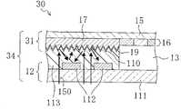
图1,表示液晶显示装置10的剖面图。液晶显示装置10,是由包括相对的彩色滤光片基板11及薄膜晶体管基板12、设置在它们之间的液晶层13(显示媒体层)、设置在相对两基板之间未图示的柱状间隔粒子的液晶显示面板14以及未图示的后照灯等构成的。FIG. 1 shows a cross-sectional view of a liquid
[0052]彩色滤光片基板(CF基板11),在玻璃基板15上形成了由赤(R)、绿(G)以及青(B)三原色形成的色层16,它们构成显示部。作为色层16,除RGB的组合外,还可以使用青绿色(cyan)、浓紫红色(magenta)、黄色(yellow)的补色。[0052] The color filter substrate (CF substrate 11) has a
[0053]在色层16上分别形成了未图示的相对电极及定向膜。色层16,在它的外周,设置为得到对比度的镶边的黑底17(遮光层)形成遮光部。在黑底17上,形成了紫外线扩散基础层18(紫外线扩散机构)。[0053] On the
[0054]紫外线扩散基础层18,是由树脂材料或陶瓷材料等形成的,其表面形成为凹凸状,构成凹凸部。表面的凹凸形状,可以是任何形状的,也可以是半球状、圆锥状、角锥状或者是柱状等的突起的多个形成的,还可以是连续起伏整个面上形成的。紫外线扩散基础层18,其表面由紫外线反射膜19覆盖构成紫外线反射面110。[0054] The ultraviolet
[0055]紫外线反射膜19,是由Al或Ag等的反射率高的金属、或是它们的合金形成的。还有,为了降低观测者一侧的反射率,在紫外线反射膜19和紫外线扩散基础层18之间设置Cr等反射率低的金属亦可。还有,同样地,紫外线反射膜19和紫外线扩散基础层18之间设置SiO2贴紧层亦可。再有,在紫外线反射膜19上,还可以设置SiO2等的保护层或增反射膜。[0055] The
[0056]薄膜晶体管基板(TFT基板12),是由玻璃基板111、玻璃基板111上分别形成的未图示的栅电极、源电极以及漏电极等的薄膜晶体管(TFT)元件、透明绝缘层、像素电极以及定向膜等构成。电连接薄膜晶体管(TFT)元件的布线中,由Al等形成的布线112,为了显示装置的窄边缘,设置在遮光部中。The thin film transistor substrate (TFT substrate 12) is a thin film transistor (TFT) element, a transparent insulating layer, a gate electrode, a source electrode, and a drain electrode, etc., which are not shown in the figure, respectively formed on the
[0057]密封材料113,设置在形成于CF基板11上的黑底17上的紫外线反射膜19和相对的薄膜晶体管(TFT)基板12之间,粘合着两基板。密封材料113,没有形成在液晶封入口,围绕着显示部不间断的连续设置,由此形成了液晶显示单元。密封材料113,是由基本聚合体的合成树脂(有机玻璃)、丙烯树脂等的紫外线固化型密封剂构成。[0057] The sealing
[0058](液晶显示装置10的制造方法)(Manufacturing method of liquid crystal display device 10)
接下来,详细说明本实施方式1所涉及的液晶显示装置10的制造方法。Next, a method of manufacturing the liquid
[0059](CF基板11的制造方法)(Manufacturing method of CF substrate 11)
首先,准备玻璃基板15。并且,玻璃基板15上成为遮光部分区域的上额边缘部10mm以下,在像素间用喷镀法等形成宽度为5至50μm的黑底17。接下来,在玻璃基板15上的成为显示部的区域的整个面上叠置分散了赤色颜料的树脂膜(干膜),进行曝光、显像以及烘烤(热处理),形成第一色层(赤)。接下来,重叠在第一色层上,整个面上叠置分散了绿色颜料的树脂薄片,进行曝光、显像以及烘烤(热处理),形成第二色层(绿)。同样,形成第三色层(青)。First, the
[0060]尚,色层16的形成方法,取代叠置干膜,通过旋转(spin)、缝隙涂层(slit coat)整面涂布分散了颜料的感光性树脂材料亦可。再有,着色层的各色形成的顺序,没有特别的限定,是其他的顺序亦可。[0060] Still, the formation method of the
[0061]接下来,色层16上镀气ITO形成相对电极,接下来形成定向膜。[0061] Next, the
[0062]接下来,在黑底17上形成薄膜层,对这个薄膜层挤压表面是多条细微的凹凸形状的的加工模型在薄膜层的表面设置凹凸形状,形成紫外线扩散基础层18。形成紫外线扩散基础层18后,以覆盖其表面的形式形成Al等的金属薄膜得到紫外线反射膜19。Next, form film layer on
[0063]通过以上的工序,完成CF基板11。[0063] Through the above steps, the
[0064]尚,作为紫外线扩散基础层18的形成方法,在表面具有多条细微凹凸形状的临时支撑体上叠层薄膜层,在黑底17上临摹薄膜层亦可。临摹薄膜的表面上扩散光得到的形成了凹凸形状面的临时支撑体,可以使用通过挤压表面是多条细微的凹凸形状的加工模型制造的。还有,设置基础薄膜能够变形的涂底层,在这个层上挤压表面是多条细微凹凸形状的加工模型,将通过固化涂底层工序形成的取代基础薄膜使用亦可。还有,基础薄膜的表面也可以使用喷砂处理的薄膜。[0064] Still, as a formation method of the ultraviolet
[0065]作为表面是多条细微的凹凸形状的加工模型或临时支撑体的制作方法之一,有以下的做法。也就是,在绝缘板上涂布光敏抗蚀剂后,或者是用具有所规定的掩模图案的光掩模曝光显像、或者是用激光切割后,在图案形成面上通过真空镀气法或喷镀法等形成(导电化处理)银或镍膜,通过电铸镍叠层,由从绝缘板剥离工序制作father原型。在这个father原型上进行剥离处理再次进行镍电铸,从father原型剥离制作母原型,通过使用这个母原型形成多数细微的凹凸,制作加工型或者支撑体。[0065] As one of the manufacturing methods of a processing model or a temporary support whose surface is a plurality of fine concavo-convex shapes, there are the following methods. That is, after coating a photosensitive resist on an insulating plate, or using a photomask with a prescribed mask pattern for exposure and development, or after cutting with a laser, vacuum vapor deposition is performed on the pattern forming surface. Form (conductive treatment) silver or nickel film by sputtering method, etc., and make father prototype by electroforming nickel lamination, and peeling off from insulating board. This father prototype is stripped and nickel electroforming is performed again, and the mother prototype is peeled off from the father prototype, and many fine unevenness is formed by using this mother prototype, and a processing type or a support body is produced.
[0066](薄膜晶体管(TFT)基板12的制造工序)(Manufacturing process of thin film transistor (TFT) substrate 12)
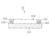
接下来,准备玻璃基板111,通过喷镀法形成由Ta或Al/Ti形成的栅电极,图案化。接下来作为栅极绝缘膜形成SiNx,作为薄膜形成半导体a-Si、p-Si或单结晶Si。接下来,作为蚀刻保护膜形成SiNx,进行图案形成。接下来形成接线柱孔、漏电极以及源电极。再有,通过同一工序或者另外的工序,在基板端部设置驱动器,形成薄膜晶体管。再有,在所规定的区域形成透明绝缘层。接下来,真空镀气ITO再图案形成,形成像素电极。接下来,经过照相平面印刷工序形成多个为规定单元厚度的柱状间隔粒子。尚,即可以是柱状间隔粒子形成在CF基板11一侧,也可以使用散布球状间隔粒子的方式。Next, a
[0067]通过以上的工序,制作薄膜晶体管(TFT)基板12。[0067] Through the above steps, the thin film transistor (TFT)
[0068](液晶显示面板14的形成工序)(Formation process of liquid crystal display panel 14)
接下来,用图11至图16说明液晶显示面板14的形成工序。Next, the steps of forming the liquid
[0069]首先,如图11所示的形成了薄膜晶体管(TFT)基板12的Al等的布线112的遮光部上,涂布如图12所示的连续不间断的密封材料113。[0069] First, as shown in FIG. 11, a continuous and
[0070]接下来,如图13所示那样,利用分配器等向薄膜晶体管(TFT)基板12滴下一滴为2mg的液晶材料114。在此之际,液晶材料114滴到薄膜晶体管(TFT)基板12的遮光部外周围涂布成框状的密封材料113内。[0070] Next, as shown in FIG. 13, a drop of 2 mg of
[0071]接下来,如图14所示那样,液晶材料114滴下的薄膜晶体管(TFT)基板12上合对位置粘合CF基板11。这时,粘合的CF基板11剂薄膜晶体管(TFT)基板12中由密封材料113围起来的区域上,形成了液晶显示单元。这个工序是在真空中进行的。接下来,返回到大气中粘合的薄膜晶体管(TFT)基板12和CF基板11之间的液晶材料114由于大气压的作用扩散。[0071] Next, as shown in FIG. 14, the
[0072]接下来,如图15所示那样,在薄膜晶体管(TFT)基板12一侧的显示部设置了遮光掩模115的状态下,从薄膜晶体管(TFT)基板12一侧照射紫外线150。照射的紫外线150,从薄膜晶体管(TFT)基板12的密封材料对应部进入,固化密封材料113。这时,薄膜晶体管(TFT)基板12的遮光部上因为设置了由Al等形成的布线112,就残留下了由这个布线112遮住紫外线150的密封材料113上未固化区域116。但是,到达密封材料113的紫外线150继续向前到达CF基板11的遮光部构成的紫外线反射面110。因为紫外线反射面110形成在形成为凹凸状的紫外线扩散基础层18的表面,所以,到达紫外线反射面110的紫外线150,在被反射的同时对应凹凸形状被扩散。[0072] Next, as shown in FIG. 15, in the state where the light-shielding
[0073]扩散反射的紫外线150,折回再次照射密封材料113的同时,在薄膜晶体管(TFT)基板12的Al等形成的布线112上也被反射,再进一步扩大的范围内照射密封材料113。为此,密封材料113的未固化区域116由反射紫外线而固化。[0073] The diffusely reflected
[0074]接下来,如图16所示那样,去除遮光掩模115,经过加热·除冷工序分断成所希望的显示面板框。[0074] Next, as shown in FIG. 16, the light-shielding
[0075]这样,液晶材料114由固化了的密封材料113密封在两枚基板之间形成液晶显示面板14,在它们上设置未图示的后照灯单元完成液晶显示装置10。[0075] In this way, the
[0076](实施方式2)(embodiment 2)
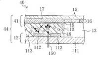
(彩色滤光片基板21及其使用它的液晶显示装置20的构成)(
图2,表示本实施方式2所涉及的液晶显示装置10的剖面图。还有,与上述实施方式所示的相同部分标注相同的符号,省略其说明。FIG. 2 is a cross-sectional view of a liquid
[0077]液晶显示装置20,是由薄膜晶体管基板12及CF基板21、具有设置在它们之间的液晶层13的液晶显示面板24、以及未图示的后照灯等构成。[0077] The liquid
[0078]CF基板21,在玻璃基板15上形成了构成显示部的色层16,未图示的相对电极及定向膜。色层16,在它的外周,形成了设置为得到对比度的镶边的黑底17的遮光部。在黑底17上,形成了紫外线扩散基础层28。[0078] The
[0079]紫外线扩散基础层28,是由树脂材料或陶瓷材料等形成的,其表面形成为凹凸状,构成凹凸部。表面的凹凸形状,向着垂直于CF基板21的显示预定区域(设置液晶层13的区域)的面,以向着它的相反一侧的区域形成了倾斜面。尚,CF基板21的凹凸形状,只要是将接受的紫外线从液晶层13向外侧反射无论任何形状均可。紫外线扩散基础层28,其表面由紫外线反射膜19覆盖着。[0079] The ultraviolet
[0080]密封材料113,设置在形成于CF基板21上的黑底17上的紫外线反射膜19和相对的薄膜晶体管(TFT)基板12之间,粘合着两基板。密封材料113,没有形成在液晶封入口,围绕着显示部不间断的连续设置,由此形成了液晶显示单元。[0080] The sealing
[0081](液晶显示装置20的制造方法)(Manufacturing method of liquid crystal display device 20)
接下来,详细说明本实施方式2所涉及的液晶显示装置20的制造方法。还有,与上述实施方式表示的相同的部分,省略其说明。Next, a method of manufacturing the liquid
[0082](CF基板21的制造方法)(Manufacturing method of CF substrate 21)
首先,与实施方式1一样,在玻璃基板15上形成色层16、黑底17、相对电极以及定向膜。First, as in the first embodiment, the
[0083]接下来,在黑底17上形成薄膜层,对这个薄膜层挤压表面是多条细微的凹凸形状的的加工模型在薄膜层的表面设置凹凸形状,形成紫外线扩散基础层28。形成紫外线扩散基础层28后,以覆盖其表面的形式形成Al等的金属薄膜得到紫外线反射膜19。Next, form film layer on
[0084]通过以上的工序,完成CF基板21。[0084] Through the above steps, the
[0085](薄膜晶体管(TFT)基板12的制造工序)(Manufacturing process of thin film transistor (TFT) substrate 12)
接下来,与实施方式1一样,形成薄膜晶体管(TFT)基板12。Next, as in the first embodiment, a thin film transistor (TFT)
[0086](液晶显示面板24的形成工序)(Formation process of liquid crystal display panel 24)
接下来,在形成了薄膜晶体管(TFT)基板12的Al等的布线112的遮光部上,涂布连续不间断的密封材料113。Next, a sealing
[0087]接下来,利用分配器等向薄膜晶体管(TFT)基板12的遮光部外周围涂布成框状的密封材料113内滴下液晶材料114。[0087] Next, the
[0088]接下来,液晶材料114滴下的薄膜晶体管(TFT)基板12上合对位置粘合CF基板21。这个工序是在真空中进行的。接下来,返回到大气中扩散液晶材料114。[0088] Next, the
[0089]接下来,在薄膜晶体管(TFT)基板12一侧的显示部设置了遮光掩模115的状态下,从薄膜晶体管(TFT)基板12一侧照射紫外线150。照射的紫外线150,从薄膜晶体管(TFT)基板12的密封材料对应部进入,固化密封材料113。这时,薄膜晶体管(TFT)基板12的遮光部上因为设置了由Al等形成的布线112,就残留下了由这个布线112遮住紫外线150的密封材料113上未固化区域116。但是,到达密封材料113的紫外线150继续向前到达CF基板21的遮光部构成的紫外线反射面110。因为紫外线反射面110形成在形成为凹凸状的紫外线扩散基础层28的表面,所以,到达紫外线反射面110的紫外线150,在被反射的同时对应凹凸形状被扩散。[0089] Next, ultraviolet rays 150 are irradiated from the thin film transistor (TFT)
[0090]扩散反射的紫外线150,折回再次照射密封材料113的同时,在薄膜晶体管(TFT)基板12的Al等形成的布线112上也被反射,再进一步扩大的范围内照射密封材料113。为此,密封材料113的未固化区域116由反射紫外线而固化。还有,因为紫外线扩散基础层28的凹凸形状是由垂直面和倾斜面构成的,所以,从液晶层1 3向外反射在其表面形成的紫外线反射膜19的表面(紫外线反射面110)接受的紫外线。因此,反射紫外线不朝液晶层13,液晶层13上不照射紫外线150。[0090] The diffusely reflected
[0091]接下来,去除遮光掩模115,经过加热·除冷工序分断成所希望的显示面板框。[0091] Next, the light-shielding
[0092]这样,液晶材料114由固化了的密封材料113密封在两枚基板之间形成液晶显示面板14,在它们上设置未图示的后照灯单元完成液晶显示装置20。[0092] In this way, the
[0093](实施方式3)(embodiment 3)
(彩色滤光片基板及其使用它的液晶显示装置20的构成)(Color Filter Substrate and Configuration of Liquid
图3,表示本实施方式3所涉及的液晶显示装置30的剖面图。还有,与上述实施方式所示相同的部分标注相同的符号,省略其说明。FIG. 3 is a cross-sectional view of a liquid
[0094]液晶显示装置30,是由薄膜晶体管(TFT)基板12及CF基板31、具有设置在它们之间的液晶层13的液晶显示面板34、以及未图示的后照灯等构成的。[0094] The liquid
[0095]CF基板31,在玻璃基板15上分别形成了色层16、未图示的相对电极以及定向膜。色层16,在它的外周,设置黑底17形成了遮光部。在黑底17上,形成了紫外线扩散基础层18(紫外线扩散机构)。[0095] The
[0096]黑底17,其表面形成为凹凸状,由它们构成紫外线扩散机构。黑底17表面的凹凸形状,可以是任何形状的,也可以是半球状、圆锥状、角锥状或者是柱状等的多个突起状形成的,还可以是小坡度连续起伏整个面上形成的。黑底17,其表面由紫外线反射膜19覆盖。[0096] The
[0097]薄膜晶体管(TFT)基板12,是由玻璃基板111、玻璃基板111上分别形成的未图示的栅电极、源电极以及漏电极等的薄膜晶体管(TFT)元件、分别未图示的透明绝缘层、像素电极以及定向膜等构成。Thin film transistor (TFT)
[0098]密封材料113,设置在形成于CF基板11上的黑底17上的紫外线反射膜19和相对的薄膜晶体管(TFT)基板12之间,粘合着两基板。密封材料113,没有形成在液晶封入口,围绕着显示部不间断的连续设置,由此形成了液晶显示单元。[0098] The sealing
[0099](液晶显示装置30的制造方法)(Manufacturing method of liquid crystal display device 30)
接下来,详细说明本实施方式3所涉及的液晶显示装置30的制造方法。还有,与上述实施方式所示相同的部分,省略其说明。Next, a method of manufacturing the liquid
[0100](CF基板31的制造方法)(Manufacturing method of CF substrate 31)
首先,与实施方式1一样,在玻璃基板15上形成色层16、黑底17、相对电极以及定向膜。First, as in the first embodiment, the
[0101]接下来,通过蚀刻黑底17的表面等的处理,形成凹凸形状。其后,以覆盖黑底17表面的形式形成Al等的金属薄膜得到紫外线反射膜19。[0101] Next, an uneven shape is formed by etching the surface of the
[0102]通过以上的工序,完成CF基板31。[0102] Through the above steps, the
[0103](薄膜晶体管(TFT)基板12的制造工序)(Manufacturing process of thin film transistor (TFT) substrate 12)
接下来,与实施方式1一样,形成薄膜晶体管(TFT)基板12。Next, as in the first embodiment, a thin film transistor (TFT)
[0104](液晶显示面板34的形成工序)(Formation process of liquid crystal display panel 34)
接下来,在形成了薄膜晶体管(TFT)基板12的Al等的布线112的遮光部上,涂布连续不间断的密封材料113。Next, a sealing
[0105]接下来,利用分配器等向薄膜晶体管(TFT)基板12的遮光部外周围涂布成框状的密封材料113内滴下液晶材料114。[0105] Next, the
[0106]接下来,液晶材料114滴下的薄膜晶体管(TFT)基板12上合对位置粘合CF基板31。这个工序是在真空中进行的。接下来,返回到大气中扩散液晶材料114。[0106] Next, the
[0107]接下来,在薄膜晶体管(TFT)基板12一侧的显示部设置了遮光掩模115的状态下,从薄膜晶体管(TFT)基板12一侧照射紫外线150。照射的紫外线150,从薄膜晶体管(TFT)基板12的密封材料对应部进入,固化密封材料113。这时,薄膜晶体管(TFT)基板12的遮光部上因为设置了由Al等形成的布线112,就残留下了由这个布线112遮住紫外线150的密封材料113上未固化区域116。但是,到达密封材料113的紫外线150继续向前到达CF基板11的遮光部构成的紫外线反射面110。因为紫外线反射面110形成在形成为凹凸状的黑底17的表面,所以,到达紫外线反射面110的紫外线150,在被反射的同时对应凹凸形状被扩散。[0107] Next, ultraviolet rays 150 are irradiated from the thin film transistor (TFT)
[0108]扩散反射的紫外线150,折回再次照射密封材料113的同时,在薄膜晶体管(TFT)基板12的Al等形成的布线112上也被反射,再进一步扩大的范围内照射密封材料113。为此,密封材料113的未固化区域116由反射紫外线而固化。[0108] The diffusely reflected
[0109]接下来,去除遮光掩模115,经过加热·除冷工序分断成所希望的显示面板框。[0109] Next, the light-shielding
[0110]这样,液晶材料114由固化了的密封材料113密封在两枚基板之间形成液晶显示面板34,在它们上设置未图示的后照灯单元完成液晶显示装置30。[0110] In this way, the
[0111](实施方式4)(Embodiment 4)
(彩色滤光片基板41及其使用它的液晶显示装置40的构成)(
图4,表示本实施方式4所涉及的液晶显示装置40的剖面图。还有,与上述实施方式所示的相同的部分标注相同的符号,省略其说明。FIG. 4 is a cross-sectional view of a liquid
[0112]液晶显示装置40,是由相对的薄膜晶体管基板12及CF基板41、具有设置在它们之间的液晶层13的液晶显示面板44、以及未图示的后照灯等构成的。[0112] The liquid
[0113]CF基板41,在玻璃基板15上分别形成了构成显示部色层16,未图示的相对电极及定向膜。色层16,在它的外周,设置黑底17形成了遮光部。在黑底17上形成了紫外线反射膜19。[0113] The
[0114]密封材料113,设置在形成于CF基板41上的黑底17上的紫外线反射膜19和相对的薄膜晶体管(TFT)基板12之间,粘合着两基板。密封材料113,没有形成在液晶封入口,围绕着显示部不间断的连续设置,由此形成了液晶显示单元。密封材料113,每100重量单位含有0.01至1.00重量单位的折射率不同的粒子48(紫外线扩散粒子)。折射率不同的粒子48,折射率,例如和密封材料113有0.03以上不同,再有,平均粒径为不影响单元厚度的值,例如1值5μm的粒子。[0114] The sealing
[0115](液晶显示装置40的制造方法)(Manufacturing method of liquid crystal display device 40)
接下来,详细说明本实施方式4所涉及的液晶显示装置40的制造方法。还有,与上述实施方式所示的相同的部分,省略其说明。Next, a method of manufacturing the liquid
[0116](CF基板41的制造方法)(Manufacturing method of CF substrate 41)
首先,与实施方式1一样,在玻璃基板15上形成色层16、黑底17、相对电极以及定向膜。First, as in the first embodiment, the
[0117]接下来,在黑底17上形成紫外线反射膜19。[0117] Next, the
[0118]通过以上的工序,完成CF基板41。[0118] Through the above steps, the
[0119](薄膜晶体管(TFT)基板12的制造工序)(Manufacturing process of thin film transistor (TFT) substrate 12)
接下来,与实施方式1一样,形成薄膜晶体管(TFT)基板12。Next, as in the first embodiment, a thin film transistor (TFT)
[0120](液晶显示面板44的形成工序)(Formation process of liquid crystal display panel 44)
接下来,在形成了薄膜晶体管(TFT)基板12的Al等的布线的遮光部上,涂布连续不间断的含有折射率不同的粒子48的密封材料113。Next, a sealing
[0121]接下来,利用分配器等向薄膜晶体管(TFT)基板12的遮光部外周围涂布成框状的密封材料113内滴下液晶材料114。[0121] Next, the
[0122]接下来,在液晶材料114滴下的薄膜晶体管(TFT)基板12上合对位置粘合CF基板41。这个工序是在真空中进行的。接下来,返回到大气中扩散液晶材料114。[0122] Next, on the thin film transistor (TFT)
[0123]接下来,在薄膜晶体管(TFT)基板12一侧的显示部设置了遮光掩模115的状态下,从薄膜晶体管(TFT)基板12一侧照射紫外线150。照射的紫外线150,从薄膜晶体管(TFT)基板12的密封材料对应部进入,固化密封材料113。这时,薄膜晶体管(TFT)基板12的遮光部上因为设置了由Al等形成的布线112,就残留下了由这个布线112遮住紫外线150的密封材料113上未固化区域116。但是,到达密封材料113的紫外线150继续向前到达CF基板41的遮光部构成的紫外线反射面110,再度照射密封材料113。[0123] Next, ultraviolet rays 150 are irradiated from the thin film transistor (TFT)
[0124]这时,因为密封材料113含有折射率不同的粒子48,所以,紫外线150,由密封材料113和折射率不同的粒子48的界面反射扩散到广范围。扩散反射的紫外线150,再次照射密封材料113的同时,在薄膜晶体管(TFT)基板12的Al等形成的布线112上也被反射,再进一步扩大的范围内照射密封材料113。为此,密封材料113的未固化区域116由反射紫外线而固化。[0124] At this time, since the sealing
[0125]接下来,去除遮光掩模115,经过加热·除冷工序分断成所希望的显示面板框。[0125] Next, the light-shielding
[0126]这样,液晶材料114由固化了的密封材料113密封在两枚基板之间形成液晶显示面板44,在它们上设置未图示的后照灯单元完成液晶显示装置40。[0126] In this way, the
[0127](实施方式5)(embodiment 5)
(彩色滤光片基板5 1及其使用它的液晶显示装置50的构成)(Configuration of
图5,表示本实施方式5所涉及的液晶显示装置50的剖面图。还有,与上述实施方式所示的相同的部分标注相同的符号,省略其说明。FIG. 5 is a cross-sectional view of a liquid
[0128]液晶显示装置50,是由相对的薄膜晶体管基板12及CF基板51、具有设置在它们之间的液晶层13的液晶显示面板54、以及未图示的后照灯等构成的。[0128] The liquid
[0129]CF基板51,在玻璃基板15上分别形成了构成显示部的色层16,未图示的相对电极及定向膜。色层16,在它的外周,设置黑底17形成了遮光部。在黑底17上形成了紫外线反射膜19。[0129] The
[0130]密封材料113,设置在形成于CF基板51上的黑底17上的紫外线反射膜19和相对的薄膜晶体管(TFT)基板12之间,粘合着两基板。密封材料113,没有形成在液晶封入口,围绕着显示部不间断的连续设置,由此形成了液晶显示单元。密封材料113,每100重量单位含有0.01至1.00重量单位的反射紫外线粒子58(紫外线扩散粒子)。反射紫外线粒子58,例如,表面处理为镜面,平均粒径为不影响单元厚度的值,例如1值5μm的粒子。[0130] The sealing
[0131](液晶显示装置50的制造方法)(Manufacturing method of liquid crystal display device 50)
接下来,详细说明本实施方式5所涉及的液晶显示装置50的制造方法。还有,与上述实施方式所示的相同的部分,省略其说明。Next, a method of manufacturing the liquid
[0132](CF基板51的制造方法)(Manufacturing method of CF substrate 51)
首先,与实施方式1一样,在玻璃基板15上形成色层16、黑底17、相对电极以及定向膜。First, as in the first embodiment, the
[0133]接下来,在黑底17上形成紫外线反射膜19。[0133] Next, the
[0134]通过以上的工序,完成CF基板51。[0134] Through the above steps, the
[0135](薄膜晶体管(TFT)基板12的制造工序)(Manufacturing process of thin film transistor (TFT) substrate 12)
接下来,与实施方式1一样,形成薄膜晶体管(TFT)基板12。Next, as in the first embodiment, a thin film transistor (TFT)
[0136](液晶显示面板54的形成工序)(Formation process of liquid crystal display panel 54)
接下来,在形成了薄膜晶体管(TFT)基板12的Al等的布线的遮光部上,涂布连续不间断的含有反射紫外线粒子58的密封材料113。Next, a sealing
[0137]接下来,利用分配器等向薄膜晶体管(TFT)基板12的遮光部外周围涂布成框状的密封材料113内滴下液晶材料114。[0137] Next, the
[0138]接下来,在液晶材料114滴下的薄膜晶体管(TFT)基板12上合对位置粘合CF基板51。这个工序是在真空中进行的。接下来,返回到大气中扩散液晶材料114。[0138] Next, on the thin film transistor (TFT)
[0139]接下来,在薄膜晶体管(TFT)基板12一侧的显示部设置了遮光掩模115的状态下,从薄膜晶体管(TFT)基板12一侧照射紫外线150。照射的紫外线150,从薄膜晶体管(TFT)基板12的密封材料对应部进入,固化密封材料113。这时,薄膜晶体管(TFT)基板12的遮光部上因为设置了由Al等形成的布线112,就残留下了由这个布线112遮住紫外线150的密封材料113上未固化区域116。但是,到达密封材料113的紫外线150继续向前到达CF基板41的遮光部构成的紫外线反射面110,再度照射密封材料113。[0139] Next, ultraviolet rays 150 are irradiated from the thin film transistor (TFT)
[0140]这时,因为密封材料113含有反射紫外线150的粒子58,所以,紫外线150,由密封材料113和反射紫外线的粒子58的界面反射扩散到广范围。扩散反射的紫外线150,再次照射密封材料113的同时,在薄膜晶体管(TFT)基板12的Al等形成的布线112上也被反射,再进一步扩大的范围内照射密封材料113。为此,密封材料113的未固化区域116由反射紫外线而固化。[0140] At this time, since the sealing
[0141]接下来,去除遮光掩模115,经过加热·除冷工序分断成所希望的显示面板框。[0141] Next, the light-shielding
[0142]这样,液晶材料114由固化了的密封材料113密封在两枚基板之间形成液晶显示面板54,在它们上设置未图示的后照灯单元完成液晶显示装置50。[0142] In this way, the
[0143](实施方式6)(Embodiment 6)
(彩色滤光片基板61及其使用它的液晶显示装置60的构成)(
图6,表示本实施方式6所涉及的液晶显示装置60的剖面图。还有,与上述实施方式所示的相同的部分标注相同的符号,省略其说明。FIG. 6 is a cross-sectional view of a liquid
[0144]液晶显示装置60,是由相对的薄膜晶体管基板12及CF基板61、具有设置在它们之间的液晶层13的液晶显示面板64、以及未图示的后照灯等构成的。[0144] The liquid
[0145]CF基板61,在玻璃基板15上分别形成了构成显示部色层16,未图示的相对电极及定向膜。色层16,在它的外周,设置黑底17形成了遮光部。在黑底17上形成了紫外线反射膜19,在紫外线反射膜19上形成了紫外线扩散层68。[0145] The
[0146]紫外线扩散层68,是由能够使紫外线透过的透明材料形成的。还有,紫外线扩散层68,还可以是由树脂材料形成的紫外线扩散树脂层。紫外线扩散层68,这层的表面与密封材料113的折射率不同,且,形成为凹凸状等的扩散紫外线的形状。[0146] The ultraviolet diffusion layer 68 is formed of a transparent material capable of transmitting ultraviolet rays. In addition, the ultraviolet diffusion layer 68 may be an ultraviolet diffusion resin layer formed of a resin material. The surface of the ultraviolet diffusion layer 68 has a different refractive index from that of the sealing
[0147]密封材料113,设置在形成于CF基板61上形成的紫外线扩散层68和相对的薄膜晶体管(TFT)基板12之间,粘合着两基板。密封材料113,没有形成在液晶封入口,围绕着显示部不间断的连续设置,由此形成了液晶显示单元。[0147] The sealing
[0148](液晶显示装置60的制造方法)(Manufacturing method of liquid crystal display device 60)
接下来,详细说明本实施方式6所涉及的液晶显示装置60的制造方法。还有,与上述实施方式所示的相同的部分,省略其说明。Next, a method of manufacturing the liquid
[0149](CF基板61的制造方法)(Manufacturing method of CF substrate 61)
首先,与实施方式1一样,在玻璃基板15上形成色层16、黑底17、相对电极以及定向膜。First, as in the first embodiment, the
[0150]接下来,在黑底17上形成紫外线反射膜19及紫外线扩散层68。[0150] Next, the
[0151]通过以上的工序,完成CF基板61。[0151] Through the above steps, the
[0152](薄膜晶体管(TFT)基板12的制造工序)(Manufacturing process of thin film transistor (TFT) substrate 12)
接下来,与实施方式1一样,形成薄膜晶体管(TFT)基板12。Next, as in the first embodiment, a thin film transistor (TFT)
[0153](液晶显示面板64的形成工序)(Formation process of liquid crystal display panel 64)
接下来,在形成了薄膜晶体管(TFT)基板12的Al等的布线的遮光部上,涂布连续不间断的密封材料113。Next, a sealing
[0154]接下来,利用分配器等向薄膜晶体管(TFT)基板12的遮光部外周围涂布成框状的密封材料113内滴下液晶材料114。[0154] Next, the
[0155]接下来,在液晶材料114滴下的薄膜晶体管(TFT)基板12上合对位置粘合CF基板61。这个工序是在真空中进行的。接下来,返回到大气中扩散液晶材料114。[0155] Next, on the thin film transistor (TFT)
[0156]接下来,在薄膜晶体管(TFT)基板12一侧的显示部设置了遮光掩模115的状态下,从薄膜晶体管(TFT)基板12一侧照射紫外线150。照射的紫外线150,从薄膜晶体管(TFT)基板12的密封材料对应部进入,固化密封材料113。这时,薄膜晶体管(TFT)基板12的遮光部上因为设置了由Al等形成的布线112,就残留下了由这个布线112遮住紫外线150的密封材料113上未固化区域116。但是,到达密封材料113的紫外线150继续向前到达CF基板61的遮光部构成的紫外线反射面110的话,到达其表面上形成的紫外线扩散层68被扩散。[0156] Next, ultraviolet rays 150 are irradiated from the thin film transistor (TFT)
[0157]扩散反射的紫外线150,再次照射密封材料113的同时,在薄膜晶体管(TFT)基板12的Al等形成的布线112上也被反射,再进一步扩大的范围内照射密封材料113。为此,密封材料113的未固化区域116由反射紫外线150而固化。[0157] The diffusely reflected
[0158]接下来,去除遮光掩模115,经过加热·除冷工序分断成所希望的显示面板框。[0158] Next, the light-shielding
[0159]这样,液晶材料114由固化了的密封材料113密封在两枚基板之间形成液晶显示面板44,在它们上设置未图示的后照灯单元完成液晶显示装置60。[0159] In this way, the
[0160](实施方式7)(Embodiment 7)
(彩色滤光片基板7 1及其使用它的液晶显示装置70的构成)(Configuration of
图7,表示本实施方式7所涉及的液晶显示装置70的剖面图。还有,与上述实施方式所示的相同的部分标注相同的符号,省略其说明。FIG. 7 is a cross-sectional view of a liquid
[0161]液晶显示装置70,是由相对的薄膜晶体管基板12及CF基板71、具有设置在它们之间的液晶层13的液晶显示面板74、以及未图示的后照灯等构成的。[0161] The liquid
[0162]CF基板71,在玻璃基板15上分别形成了构成显示部色层16,未图示的相对电极及定向膜。色层16,在它的外周,设置黑底17形成了遮光部。在黑底17上形成了紫外线反射膜19。[0162] The
[0163]在紫外线反射膜19上,形成了多个透镜构成的层(微透镜层78)。微透镜层78,是由能够透过紫外线的透明材料形成的。[0163] On the
[0164]密封材料113,设置在形成于CF基板71上形成的微透镜层78和相对的薄膜晶体管(TFT)基板12之间,粘合着两基板。密封材料113,没有形成在液晶封入口,围绕着显示部不间断的连续设置,由此形成了液晶显示单元。[0164] The sealing
[0165](液晶显示装置70的制造方法)(Manufacturing method of liquid crystal display device 70)
接下来,详细说明本实施方式7所涉及的液晶显示装置70的制造方法。还有,与上述实施方式所示的相同的部分,省略其说明。Next, a method of manufacturing the liquid
[0166](CF基板71的制造方法)(Manufacturing method of CF substrate 71)
首先,与实施方式1一样,在玻璃基板15上形成色层16、黑底17、相对电极以及定向膜。First, as in the first embodiment, the
[0167]接下来,在黑底17上形成紫外线反射膜19及微透镜层78。[0167] Next, the
[0168]通过以上的工序,完成CF基板71。[0168] Through the above steps, the
[0169](薄膜晶体管(TFT)基板12的制造工序)(Manufacturing process of thin film transistor (TFT) substrate 12)
接下来,与实施方式1一样,形成薄膜晶体管(TFT)基板12。Next, as in the first embodiment, a thin film transistor (TFT)
[0170](液晶显示面板74的形成工序)(Formation process of liquid crystal display panel 74)
接下来,在形成了薄膜晶体管(TFT)基板12的Al等的布线的遮光部上,涂布连续不间断的密封材料113。Next, a sealing
[0171]接下来,利用分配器等向薄膜晶体管(TFT)基板12的遮光部外周围涂布成框状的密封材料113内滴下液晶材料114。[0171] Next, the
[0172]接下来,在液晶材料114滴下的薄膜晶体管(TFT)基板12上合对位置粘合CF基板71。这个工序是在真空中进行的。接下来,返回到大气中扩散液晶材料114。[0172] Next, on the thin film transistor (TFT)
[0173]接下来,在薄膜晶体管(TFT)基板12一侧的显示部设置了遮光掩模115的状态下,从薄膜晶体管(TFT)基板12一侧照射紫外线150。照射的紫外线150,从薄膜晶体管(TFT)基板12的密封材料对应部进入,固化密封材料113。这时,薄膜晶体管(TFT)基板12的遮光部上因为设置了由Al等形成的布线112,就残留下了由这个布线112遮住紫外线150的密封材料113上未固化区域116。但是,到达密封材料113的紫外线150继续向前到达CF基板71的遮光部构成的紫外线反射面110的话,到达其表面上形成的微透镜层78被扩散。[0173] Next, ultraviolet rays 150 are irradiated from the thin film transistor (TFT)
[0174]扩散反射的紫外线150,再次照射密封材料113的同时,在薄膜晶体管(TFT)基板12的Al等形成的布线112上也被反射,再进一步扩大的范围内照射密封材料113。为此,密封材料113的未固化区域116由反射紫外线150而固化。[0174] The diffusely reflected
[0175]接下来,去除遮光掩模115,经过加热·除冷工序分断成所希望的显示面板框。[0175] Next, the light-shielding
[0176]这样,液晶材料114由固化了的密封材料113密封在两枚基板之间形成液晶显示面板44,在它们上设置未图示的后照灯单元完成液晶显示装置70。[0176] In this way, the
[0177](实施方式8)(Embodiment 8)
(彩色滤光片基板及其使用它的液晶显示装置80的构成)(Colour Filter Substrate and Configuration of Liquid
图8,表示本实施方式8所涉及的液晶显示装置80的剖面图。还有,与上述实施方式所示的相同的部分标注相同的符号,省略其说明。FIG. 8 is a cross-sectional view of a liquid
[0178]液晶显示装置80,是由相对的薄膜晶体管基板12及CF基板81、具有设置在它们之间的液晶层13的液晶显示面板84、以及未图示的后照灯等构成的。[0178] The liquid
[0179]CF基板81,在玻璃基板15上分别形成了构成显示部色层16,未图示的相对电极、定向膜以及柱状间隔粒子120。色层16,在它的外周,设置黑底17形成了遮光部。在黑底17上形成了紫外线反射膜19,在紫外线反射膜19上形成了紫外线扩散层88。[0179] The
[0180]紫外线扩散层88,是由能够使紫外线透过的透明材料形成的。还有,上述柱状间隔粒子120也由这个透明材料形成。紫外线扩散层88,其表面形成为凹凸状等的扩散紫外线的形状。[0180] The
[0181]密封材料113,设置在形成于CF基板81上形成的紫外线扩散层88和相对的薄膜晶体管(TFT)基板12之间,粘合着两基板。密封材料113,没有形成在液晶封入口,围绕着显示部不间断的连续设置,由此形成了液晶显示单元。[0181] The sealing
[0182](液晶显示装置80的制造方法)(Manufacturing method of liquid crystal display device 80)
接下来,详细说明本实施方式8所涉及的液晶显示装置80的制造方法。还有,与上述实施方式所示的相同的部分,省略其说明。Next, a method of manufacturing the liquid
[0183](CF基板81的制造方法)(Manufacturing method of CF substrate 81)
首先,与实施方式1一样,在玻璃基板15上形成色层16、黑底17、相对电极以及定向膜。这时,在黑底17上形成紫外线反射膜19。First, as in the first embodiment, the
[0184]接下来,用相同材料在同一工序中形成柱状间隔粒子120及紫外线扩散层88。[0184] Next, the
[0185]通过以上的工序,完成CF基板81。[0185] Through the above steps, the
[0186](薄膜晶体管(TFT)基板12的制造工序)(Manufacturing process of thin film transistor (TFT) substrate 12)
接下来,与实施方式1一样,形成薄膜晶体管(TFT)基板12。这时,还可以在薄膜晶体管(TFT)基板12上再形成柱状间隔粒子120。Next, as in the first embodiment, a thin film transistor (TFT)
[0187](液晶显示面板84的形成工序)(Formation process of liquid crystal display panel 84)
接下来,在形成了薄膜晶体管(TFT)基板12的Al等的布线的遮光部上,涂布连续不间断的密封材料113。Next, a sealing
[0188]接下来,利用分配器等向薄膜晶体管(TFT)基板12的遮光部外周围涂布成框状的密封材料113内滴下液晶材料114。[0188] Next, the
[0189]接下来,在液晶材料114滴下的薄膜晶体管(TFT)基板12上合对位置粘合CF基板81。这个工序是在真空中进行的。接下来,返回到大气中扩散液晶材料114。[0189] Next, on the thin film transistor (TFT)
[0190]接下来,与实施方式6一样通过紫外线150固化密封材料113后,完成液晶显示装置80。[0190] Next, after the sealing
[0191]尚,本实施方式8中,作为紫外线扩散机构使用了与实施方式6(紫外线扩散层68)相同的构造,但是,并不限于此,还可以是实施方式1或2所使用的方法。即便是在这种情况下,紫外线扩散机构及柱状间隔粒子120可以用相同的材料在同一工序中形成。[0191] Still, in the present embodiment 8, the same structure as that of embodiment 6 (ultraviolet diffusion layer 68) is used as the ultraviolet diffusion mechanism, but it is not limited thereto, and the method used in embodiment 1 or 2 may also be used. . Even in this case, the ultraviolet diffusion mechanism and the
[0192](实施方式9)(Embodiment 9)
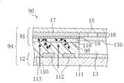
(彩色滤光片基板91及其使用它的液晶显示装置90的构成)(
图9,表示本实施方式9所涉及的液晶显示装置90的剖面图。还有,与上述实施方式所示的相同的部分标注相同的符号,省略其说明。FIG. 9 shows a cross-sectional view of a liquid
[0193]液晶显示装置90,是由相对的薄膜晶体管基板12及CF基板91、具有设置在它们之间的液晶层13的液晶显示面板94、以及未图示的后照灯等构成的。[0193] The liquid
[0194]CF基板91,在玻璃基板15上分别形成了构成显示部色层16,覆盖层130、未图示的相对电极及定向膜。色层16,在它的外周,设置黑底17形成了遮光部。在黑底17上形成了紫外线反射膜19,在紫外线反射膜19上形成了紫外线扩散层98。[0194] The
[0195]紫外线扩散层98,是由能够使紫外线透过的透明材料形成的。还有,上述覆盖层130也由这个透明材料形成。[0195] The
[0196]密封材料113,设置在形成于CF基板91上形成的紫外线扩散层98和相对的薄膜晶体管(TFT)基板12之间,粘合着两基板。密封材料113,没有形成在液晶封入口,围绕着显示部不间断的连续设置,由此形成了液晶显示单元。[0196] The sealing
[0197](液晶显示装置90的制造方法)(Manufacturing method of liquid crystal display device 90)
接下来,详细说明本实施方式9所涉及的液晶显示装置90的制造方法。还有,与上述实施方式所示的相同的部分,省略其说明。Next, a method of manufacturing the liquid
[0198](CF基板91的制造方法)(Manufacturing method of CF substrate 91)
首先,在玻璃基板15上分别形成色层16及黑底17。First, the
[0199]接下来,用相同材料在同一工序,在色层16上形成覆盖层130,在黑底17上形成紫外线扩散层98。[0199] Next, the
[0200]接下来,在覆盖层130上形成相对电极以及定向膜。[0200] Next, an opposite electrode and an alignment film are formed on the
[0201]通过以上的工序,完成CF基板91。[0201] Through the above steps, the
[0202](薄膜晶体管(TFT)基板12的制造工序)(Manufacturing process of thin film transistor (TFT) substrate 12)
接下来,与实施方式1一样,形成薄膜晶体管(TFT)基板12。Next, as in the first embodiment, a thin film transistor (TFT)
[0203](液晶显示面板94的形成工序)(Formation process of liquid crystal display panel 94)
接下来,在形成了薄膜晶体管(TFT)基板12的Al等的布线的遮光部上,涂布连续不间断的密封材料113。Next, a sealing
[0204]接下来,利用分配器等向薄膜晶体管(TFT)基板12的遮光部外周围涂布成框状的密封材料113内滴下液晶材料114。[0204] Next, the
[0205]接下来,在液晶材料114滴下的薄膜晶体管(TFT)基板12上合对位置粘合CF基板91。这个工序是在真空中进行的。接下来,返回到大气中扩散液晶材料114。[0205] Next, on the thin film transistor (TFT)
[0206]接下来,与实施方式6一样通过紫外线150固化密封材料113后,完成液晶显示装置90。[0206] Next, after the sealing
[0207]尚,本实施方式9中,作为紫外线扩散机构使用了与实施方式6(紫外线扩散层68)相同的构造,但是,并不限于此,还可以是实施方式1或2所使用的方法。即便是在这种情况下,紫外线扩散机构及覆盖层130可以用相同的材料在同一工序中形成。[0207] Still, in the present embodiment 9, the same structure as that of embodiment 6 (ultraviolet diffusion layer 68) is used as the ultraviolet diffusion mechanism, but it is not limited thereto, and the method used in embodiment 1 or 2 may also be used. . Even in this case, the ultraviolet diffusion mechanism and the
[0208](实施方式10)(Embodiment 10)
(彩色滤光片基板101及其使用它的液晶显示装置100的构成)(Configuration of
图10,表示本实施方式10所涉及的液晶显示装置100的剖面图。这个液晶显示装置100,是能够进行透过模式的显示和反射模式的显示双方的半透过性液晶显示装置。FIG. 10 is a cross-sectional view of a liquid
[0209]液晶显示装置100,是由相对的薄膜晶体管基板12及CF基板101、具有设置在它们之间的液晶层13的液晶显示面板104、以及未图示的后照灯等构成的。[0209] The liquid
[0210]CF基板101,是由玻璃基板15、在玻璃基板15上形成的色层16、未图示的相对电极、台阶层以及定向膜构成的。色层16,在它的外周,设置黑底17形成了遮光部。台阶层140,具有所规定的厚度并形成在应当成为CF基板101的反射区域的区域。台阶层140的厚度,最好的是近似液晶层13的厚度的一半。相对于反射模式中用于显示的光两次通过液晶层13,而反射模式中用于显示的光只是一次通过液晶层13。因此,如果将光透过显示部分的液晶层13的厚度设定成光反射显示部分的液晶层13的厚度的两倍,两者的光路长度就会相等,就可以由双方的显示模式实现良好的显示。[0210] The
[0211]在黑底17上形成了紫外线反射膜19及紫外线扩散层108。[0211] On the
[0212]薄膜晶体管(TFT)基板12,是在玻璃基板111上形成未图示的薄膜晶体管(TFT)元件及像素电极141构成显示部。在显示部的成为其反射区域的区域上,形成了树脂层的凹凸形状及Al及还有Al的金属膜构成的反射层142,以覆盖反射层142的方式形成未图示的透明绝缘层在表面上平整反射层142的凹凸形状。在透明绝缘层的平整的表面上,形成了定向膜。[0212] The thin film transistor (TFT)
[0213]密封材料113,设置在形成于CF基板101上形成的紫外线扩散层108和相对的薄膜晶体管(TFT)基板12之间,粘合着两基板。密封材料113,没有形成在液晶封入口,围绕着显示部不间断的连续设置,由此形成了液晶显示单元。[0213] The sealing
[0214](液晶显示装置100的制造方法)(Manufacturing method of liquid crystal display device 100)
接下来,详细说明本实施方式10所涉及的液晶显示装置100的制造方法。还有,与上述实施方式所示的相同的部分,省略其说明。Next, a method of manufacturing the liquid
[0215](CF基板101的制造方法)(Manufacturing method of CF substrate 101)
首先,在玻璃基板15上形成色层16、黑底17、以及相对电极。这时,在黑底17上形成紫外线反射膜19。First, the
[0216]接下来,用相同材料在同一工序中形成台阶层140及紫外线扩散层108,在相对电极及台阶层140上形成定向膜。[0216] Next, the stepped
[0217]通过以上的工序,完成CF基板101。[0217] Through the above steps, the
[0218](薄膜晶体管(TFT)基板12的制造工序)(Manufacturing process of thin film transistor (TFT) substrate 12)
接下来,与实施方式1一样,形成薄膜晶体管(TFT)基板12。Next, as in the first embodiment, a thin film transistor (TFT)
[0219](液晶显示面板104的形成工序)(Formation process of liquid crystal display panel 104)
接下来,在形成了薄膜晶体管(TFT)基板12的Al等的布线的遮光部上,涂布连续不间断的密封材料113。Next, a sealing
[0220]接下来,利用分配器等向薄膜晶体管(TFT)基板12的遮光部外周围涂布成框状的密封材料113内滴下液晶材料114。[0220] Next, the
[0221]接下来,在液晶材料114滴下的薄膜晶体管(TFT)基板12上合对位置粘合CF基板101。这个工序是在真空中进行的。接下来,返回到大气中扩散液晶材料114。[0221] Next, on the thin film transistor (TFT)
[0222]接下来,与实施方式6一样通过紫外线150固化密封材料113后,完成液晶显示装置100。[0222] Next, the liquid
[0223]尚,本实施方式8中,作为紫外线扩散机构使用了与实施方式6(紫外线扩散层68)相同的构造(紫外线扩散层108),但是,并不限于此,还可以是实施方式1或2所使用的方法。即便是在这种情况下,紫外线扩散机构及台阶层140可以用相同的材料在同一工序中形成。[0223] Still, in the present embodiment 8, the same structure (ultraviolet diffusion layer 108) as that of embodiment 6 (ultraviolet diffusion layer 68) is used as the ultraviolet diffusion mechanism, but it is not limited thereto, and it can also be the or 2 the method used. Even in this case, the ultraviolet diffusion mechanism and the stepped
[0224]还有,液晶显示面板14至104,也可以不形成为本实施方式那样,而是在紫外线固化型树脂密封的液晶显示面板侧面设置液晶注入口,从那里注入液晶,再用紫外线固化型树脂密封。[0224] Also, the liquid
[0225]再有,本实施方式,作为彩色滤光片基板及使用它的显示装置,表示了LCD(liquid crystal display:液晶显示面板)系列,但是,PD(plasma display:等离子显示面板)、PALC(plasma addressed liquid crystaldisplay:等离子地址液晶显示面板)、有机EL(organic electro luminescence)、无机EL(inorganic electro luminescence)、FED(field emissiondisplay:电场释放显示面板)、或者SED(surface-conduction electron-emitter display:表面电场显示面板)等系列均可。Furthermore, in this embodiment, LCD (liquid crystal display: liquid crystal display panel) series is shown as a color filter substrate and a display device using it, but PD (plasma display: plasma display panel), PALC (plasma addressed liquid crystal display: plasma address liquid crystal display panel), organic EL (organic electro luminescence), inorganic EL (inorganic electro luminescence), FED (field emission display: electric field release display panel), or SED (surface-conduction electron-emitter display : surface electric field display panel) and other series are available.
[0226](作用效果)(action effect)
接下来,说明作用效果。Next, the operation effect will be described.
[0227]本实施方式1至10所涉及的显示装置10至100,是包括相互相对设置的CF基板11至101及薄膜晶体管(TFT)基板12、和以夹在它们之间的方式设置的液晶层13的液晶显示装置,是以:液晶层13,外部由CF基板11至101及薄膜晶体管(TFT)基板12间设置的紫外线固化型树脂形成的密封材料113密封,CF基板11至101,密封材料113的对应部分设置了黑底17形成了遮光部,另一方面,薄膜晶体管(TFT)基板12,密封材料113的对应部分形成为透明地,遮光部,密封材料113一侧的面构成紫外线反射面110,为特征的。[0227] The
[0228]只要根据这样的构成,在设置了黑底17的遮光部上设置了由紫外线固化型树脂形成的密封材料113的液晶显示装置中,通过紫外线照射密封这个CF基板11至101和薄膜晶体管(TFT)基板12。在此之际,是从形成为透明地薄膜晶体管(TFT)基板12的密封材料对应部照射紫外线固化密封材料113的,但是,从薄膜晶体管(TFT)基板12一侧照射的紫外线由在CF基板11至101的遮光部上构成的紫外线反射面110向密封材料113反射,再次照射密封材料113。为此,即便是在基板上存在形成的布线用Al等妨碍紫外线射向密封材料113的物件,通过从紫外线反射面110再次紫外线照射密封材料113就能使密封材料113未固化的部分固化。因此,通过通常的紫外线照射,能够更有效且更容易的进行密封材料113的固化。[0228] According to such a configuration, in the liquid crystal display device in which the sealing
[0229]还有,本实施方式所涉及的液晶显示装置10至100,紫外线反射面110还可以是由铝或银形成的。[0229] In addition, in the liquid
[0230]只要根据这样的构成,因为紫外线反射面110是由铝或银形成的,紫外线反射面110的反射率增高,能够更有效且更容易的进行密封材料113的固化。[0230] According to such a configuration, since the
[0231]再有,本实施方式所涉及的液晶显示装置20,紫外线反射面110,还可以构成为将接收的紫外线从液晶层13向外反射。[0231] Furthermore, in the liquid
[0232]只要根据这样的构成,能够抑制由紫外线反射面110反射的紫外线射入液晶层13。为此,就能够控制液晶受到紫外线的影响给与显示品位的坏影响。[0232] According to such a configuration, the ultraviolet rays reflected by the
[0233]还有,本实施方式所涉及的液晶显示装置10至100,还可以有扩散由紫外线反射面110反射的紫外线的紫外线扩散机构18至108。[0233] In addition, the liquid
[0234]只要根据这样的构成,通过由紫外线扩散机构18至108扩散由紫外线反射面110反射的紫外线,可以向被遮光而未固化残留的密封材料113更有效的照射紫外线。因此,就能够有效且容易的固化密封材料113的全部区域。[0234] According to such a configuration, by diffusing the ultraviolet rays reflected by the
[0235]再有,本实施方式所涉及的液晶显示装置10至30,紫外线扩散机构是在遮光部形成的凹凸部,紫外线反射面110还可以形成在凹凸部上。[0235] Furthermore, in the liquid
[0236]只要根据这样的构成,因为紫外线扩散机构是在遮光部形成的凹凸部,紫外线反射面110又形成在凹凸部上,所以,到达紫外线反射面110的紫外线被反射的同时对应凹凸部被散射。为此,就能够更有效且容易的固化密封材料113的全部区域。As long as according to such constitution, because the ultraviolet diffusion mechanism is the concavo-convex part that is formed in light-shielding part, and ultraviolet
[0237]还有,本实施方式所涉及的液晶显示装置30,凹凸部还可以是由遮光部的黑底17形成的。[0237] In addition, in the liquid
[0238]只要根据这样的构成,因为凹凸部是由遮光部的黑底17形成的,所以,作为凹凸部也可以不使用新的部件,只要将黑底17形成为凹凸部既可。为此,就可以有效的形成紫外线扩散机构。[0238] According to such a configuration, since the concavo-convex part is formed by the
[0239]再有,本实施方式所涉及的液晶显示装置40、50,紫外线扩散机构,还可以是由在密封材料113中含有的紫外线扩散粒子48、58构成的。[0239] Furthermore, in the liquid
[0240]只要根据这样的构成,通过将紫外线扩散粒子48、58预先掺入密封材料113中,在通过将密封材料113提供基板就能够同时进行紫外线扩散机构的设置。为此,制造工序中效率变好的有利点。再有,将紫外线扩散粒子48、58掺入密封材料113的话,因为可以使紫外线扩散机构均匀的混入密封材料113中,能够更有效的进行紫外线的扩散。[0240] According to such a configuration, by doping the
[0241]还有,本实施方式所涉及的液晶显示装置40,还可以是紫外线扩散粒子与密封材料113折射率不同的粒子48。[0241] In addition, in the liquid
[0242]只要根据这样的构成,因为紫外线扩散粒子是与密封材料113折射率不同的粒子48,所以,密封材料113和紫外线扩散粒子的界面紫外线折射就能更有效的扩散到密封材料113整体。[0242] As long as according to such a constitution, since the ultraviolet diffusing particles are
[0243]再有,本实施方式所涉及的液晶显示装置50,紫外线扩散粒子还可以是反射紫外线的粒子58。[0243] Furthermore, in the liquid
[0244]只要根据这样的构造,因为紫外线扩散粒子是反射紫外线的粒子58,所以,由紫外线扩散粒子紫外线就能更有效的扩散到密封材料113整体。[0244] According to such a structure, since the ultraviolet diffusing particles are
[0245]还有,本实施方式所涉及的液晶显示装置60至100,紫外线反射面110及紫外线扩散机构68至108,还可以按照这个顺序设置在黑底17上。[0245] Also, the liquid
[0246]只要根据这样的构造,因为紫外线反射面110及紫外线扩散机构68至108按照这个顺序设置在黑底17上,所以,紫外线由紫外线反射面110反射后,再由紫外线扩散机构68至108扩散。因此,密封材料113整体上充分的照满紫外线,就能够更有效的固化密封材料113。As long as according to such structure, because the
[0247]再有,本实施方式所涉及的液晶显示装置60、80至100,紫外线扩散机构还可以是紫外线扩散树脂层68、88至108。[0247] Furthermore, in the liquid
[0248]只要根据这样的构造,因为紫外线扩散机构是紫外线扩散树脂层68、88至108,所以,紫外线扩散机构的形状,就能够容易的制作所希望的形状。因此,就可以容易的向密封材料113整体或有选择地向所希望的位置扩散紫外线。[0248] According to such a structure, since the ultraviolet diffusion mechanism is the ultraviolet diffusion resin layers 68, 88 to 108, the shape of the ultraviolet diffusion mechanism can be easily produced into a desired shape. Therefore, ultraviolet rays can be easily diffused to the
[0249]还有,本实施方式所涉及的液晶显示装置70,紫外线扩散机构还可以是与密封材料113折射率不同的凹凸层78。[0249] In addition, in the liquid
[0250]只要根据这样的构造,因为紫外线扩散机构是与密封材料113折射率不同的凹凸层78,所以,反射的紫外线由于密封材料113和凹凸层78的界面的折射扩散而在密封材料113整体上照射充分的紫外线,就可以有效的固化密封材料113。[0250] According to such a structure, since the ultraviolet diffusion mechanism is the concave-
[0251]再有,本实施方式所涉及的液晶显示装置70,紫外线扩散机构还可以是微透镜层78。[0251] Furthermore, in the liquid
[0252]只要根据这样的构成,因为紫外线扩散机构是微透镜层78,所以,由简单的构造就能够形成紫外线扩散机构。[0252] According to such a configuration, since the ultraviolet diffusion mechanism is the
[0253]还有,本实施方式所涉及的液晶显示装置80,在CF基板101及薄膜晶体管(TFT)基板12之间设置柱状间隔粒子120的同时,柱状间隔粒子120还可以用与紫外线扩散机构88相同的材料形成。Also, in the liquid
[0254]只要根据这样的构造,因为在CF基板101及薄膜晶体管(TFT)基板12之间设置柱状间隔粒子120的同时,柱状间隔粒子120还用与紫外线扩散机构88相同的材料形成,所以,在同一工序用相同的材料能够分别形成柱状间隔粒子120和紫外线扩散机构88。为此,装置的制造效率良好。As long as according to such a structure, because the
[0255]再有,本实施方式所涉及的液晶显示装置90,显示部的显示元件被覆盖层130覆盖的同时,覆盖层130还可以与紫外线扩散机构98用相同材料形成。[0255] Furthermore, in the liquid
[0256]只要根据这样的构造,显示部的显示元件被覆盖层130覆盖的同时,覆盖层130还与紫外线扩散机构98用相同材料形成,所以,在同一工序用相同的材料可以分别形成覆盖层130和紫外线扩散机构98。为此,装置的制造效率良好。As long as according to such structure, when the display elements of the display portion are covered by the
[0257]还有,本实施方式所涉及的液晶显示装置100,在显示部是由为限制CF基板101和薄膜晶体管(TFT)基板12的基板间隙而设置了台阶层140的光反射区域和光透过区域构成的同时,设置在光反射区域的台阶层140还可以是和紫外线扩散机构108用相同的材料形成。[0257] Also, in the liquid
[0258]只要根据这样的构造,因为在显示部是由为限制CF基板101和薄膜晶体管(TFT)基板12的基板间隙而设置了台阶层140的光反射区域和光透过区域构成的同时,设置在光反射区域的台阶层140还是和紫外线扩散机构108用相同的材料形成的,所以,在同一工序用相同的材料可以分别形成设置在光反射区域的台阶层140和紫外线扩散机构108。为此,装置的制造效率良好。[0258] According to such a structure, since the display portion is composed of a light reflection region and a light transmission region in which the
[0259]本实施方式所涉及的液晶显示装置10至100的制造方法,各自都以包括:准备具有显示单元形成预定部的CF基板11至101及薄膜晶体管(TFT)基板12的步骤;为将CF基板11至101的显示单元形成部围成封闭状态在CF基板11至101上形成黑底17的步骤;在CF基板11至101上形成的黑底17上设置紫外线反射面110的步骤;在CF基板11至101或薄膜晶体管(TFT)基板12上的遮光部预留部上不间断的设置密封材料113的步骤;在设置了密封材料113的CF基板11至101或薄膜晶体管(TFT)基板12的显示单元形成预定部中供给液晶材料114的步骤;粘合CF基板11至101及薄膜晶体管(TFT)基板12中供给了液晶材料114的一方和另一方的步骤;从粘合的薄膜晶体管(TFT)基板12的表面向密封材料113照射紫外线固化密封材料113制作粘合基板的步骤;为特征的。[0259] The manufacturing methods of the liquid
[0260]根据这样的构成,在设置了黑底17的遮光部上设置了由紫外线固化型树脂形成的密封材料113的液晶显示装置中,通过用紫外线照射这个CF基板11至101合薄膜晶体管(TFT)基板12固化密封材料113密封它们。在此之际,从薄膜晶体管(TFT)基板12一侧照射的紫外线由CF基板11至101的遮光部上构成的紫外线反射面110反射向密封材料113,再次照射密封材料113。为此,即便是在基板上形成布线用Al等妨碍紫外线向密封材料113进入的物件存在,通过从紫外线反射面110紫外线再次照射密封材料113就能够固化密封材料113的未固化部分。因此,通过通常的紫外线照射,就能够更有效且更容易的进行密封材料113的固化。According to such a configuration, in the liquid crystal display device in which the sealing
[0261]本实施方式所涉及的彩色滤光片基板11至101,是以包括:包含显示部的玻璃基板15;沿着玻璃基板15上的显示部外周设置的构成遮光部的黑底17;设置在玻璃基板15上的黑底17上的紫外线反射面110;为特征的。[0261] The
[0262]只要根据这样的构造,在设置了黑底17的遮光部上设置了由紫外线固化型树脂形成的密封材料113的液晶显示装置中,存在着以下的有利点。也就是,通过紫外线照射密封这个彩色滤光片基板11至101合薄膜晶体管(TFT)基板12时,从薄膜晶体管(TFT)基板12的密封材料对应部照射紫外线固化密封材料113。在此之际,从薄膜晶体管(TFT)基板12一侧照射的紫外线通过构成彩色滤光片基板11至101的遮光部的紫外线反射面110向密封材料113反射,再次照射密封材料113。为此,即便是在薄膜晶体管(TFT)基板12上形成有布线用Al等妨碍紫外线向密封材料113进入的物件存在,通过从紫外线反射面110紫外线再次照射密封材料113就能够固化密封材料113的未固化部分。因此,通过通常的紫外线照射,就能够更有效且更容易的进行密封材料113的固化。[0262] According to such a structure, the liquid crystal display device in which the sealing
-产业上利用的可能性--Possibility of industrial use-
[0263]通过以上的说明,本发明,对显示装置、显示装置的制造方法、基板及彩色滤光片基板是有用的。[0263] As described above, the present invention is useful for a display device, a method for manufacturing a display device, a substrate, and a color filter substrate.
Claims (19)
Translated fromChineseApplications Claiming Priority (2)
| Application Number | Priority Date | Filing Date | Title |
|---|---|---|---|
| JP015066/2006 | 2006-01-24 | ||
| JP2006015066 | 2006-01-24 |
Related Child Applications (1)
| Application Number | Title | Priority Date | Filing Date |
|---|---|---|---|
| CN2011100931758ADivisionCN102162954A (en) | 2006-01-24 | 2006-08-11 | Display device, display device manufacturing method, substrate, and color filter substrate |
Publications (1)
| Publication Number | Publication Date |
|---|---|
| CN101297236Atrue CN101297236A (en) | 2008-10-29 |
Family
ID=38308968
Family Applications (2)
| Application Number | Title | Priority Date | Filing Date |
|---|---|---|---|
| CN2011100931758APendingCN102162954A (en) | 2006-01-24 | 2006-08-11 | Display device, display device manufacturing method, substrate, and color filter substrate |
| CNA200680039518XAPendingCN101297236A (en) | 2006-01-24 | 2006-08-11 | Display device, method for manufacturing display device, substrate, and color filter substrate |
Family Applications Before (1)
| Application Number | Title | Priority Date | Filing Date |
|---|---|---|---|
| CN2011100931758APendingCN102162954A (en) | 2006-01-24 | 2006-08-11 | Display device, display device manufacturing method, substrate, and color filter substrate |
Country Status (3)
| Country | Link |
|---|---|
| US (1) | US20090231524A1 (en) |
| CN (2) | CN102162954A (en) |
| WO (1) | WO2007086159A1 (en) |
Cited By (14)
| Publication number | Priority date | Publication date | Assignee | Title |
|---|---|---|---|---|
| CN102376512A (en)* | 2010-09-30 | 2012-03-14 | 四川虹欧显示器件有限公司 | Plasma screen and manufacturing method thereof |
| CN103676339A (en)* | 2013-12-18 | 2014-03-26 | 合肥京东方光电科技有限公司 | Color membrane substrate and manufacturing method thereof |
| CN103885252A (en)* | 2014-03-12 | 2014-06-25 | 京东方科技集团股份有限公司 | Display panel and display device |
| CN104635394A (en)* | 2015-02-13 | 2015-05-20 | 深圳市华星光电技术有限公司 | Array substrate and liquid crystal display panel |
| TWI504980B (en)* | 2012-07-24 | 2015-10-21 | Innocom Tech Shenzhen Co Ltd | Liquid-crystal panel and the uv curing method thereof |
| CN106249487A (en)* | 2016-08-19 | 2016-12-21 | 深圳市华星光电技术有限公司 | A kind of color membrane substrates and display device |
| CN106873231A (en)* | 2011-07-11 | 2017-06-20 | 大日本印刷株式会社 | Colored filter forms substrate and preparation method thereof and display device |
| CN107193409A (en)* | 2016-03-14 | 2017-09-22 | 三星显示有限公司 | The assemble method and display device of display device |
| CN109507825A (en)* | 2018-12-19 | 2019-03-22 | 惠科股份有限公司 | Display panel and display panel manufacturing method |
| JP2020144380A (en)* | 2018-05-23 | 2020-09-10 | セイコーエプソン株式会社 | Electro-optical device and electronic apparatus |
| WO2021248663A1 (en)* | 2020-06-12 | 2021-12-16 | 惠州市华星光电技术有限公司 | Display panel, touch display device, and manufacturing method therefor |
| JP2022020861A (en)* | 2018-05-23 | 2022-02-01 | セイコーエプソン株式会社 | Electro-optical device and electronic apparatus |
| CN114265247A (en)* | 2021-12-20 | 2022-04-01 | 绵阳惠科光电科技有限公司 | Packaging adhesive, display panel and display device |
| CN114709348A (en)* | 2022-03-31 | 2022-07-05 | 武汉天马微电子有限公司 | Display modules and display devices |
Families Citing this family (42)
| Publication number | Priority date | Publication date | Assignee | Title |
|---|---|---|---|---|
| US7855824B2 (en) | 2004-03-06 | 2010-12-21 | Qualcomm Mems Technologies, Inc. | Method and system for color optimization in a display |
| US7911428B2 (en) | 2004-09-27 | 2011-03-22 | Qualcomm Mems Technologies, Inc. | Method and device for manipulating color in a display |
| US7928928B2 (en) | 2004-09-27 | 2011-04-19 | Qualcomm Mems Technologies, Inc. | Apparatus and method for reducing perceived color shift |
| US8004743B2 (en) | 2006-04-21 | 2011-08-23 | Qualcomm Mems Technologies, Inc. | Method and apparatus for providing brightness control in an interferometric modulator (IMOD) display |
| JP5121358B2 (en)* | 2007-08-31 | 2013-01-16 | 株式会社ジャパンディスプレイウェスト | Light receiving device and electro-optical device including light receiving device |
| JP5243811B2 (en)* | 2008-02-14 | 2013-07-24 | セイコーインスツル株式会社 | Display device |
| JP2010197967A (en)* | 2009-02-27 | 2010-09-09 | Sony Corp | Method for manufacturing liquid crystal display device and liquid crystal display device manufactured by the same |
| KR101549258B1 (en)* | 2009-03-11 | 2015-09-01 | 엘지전자 주식회사 | Display device |
| KR101549256B1 (en)* | 2009-03-11 | 2015-09-01 | 엘지전자 주식회사 | Display device |
| KR101549257B1 (en)* | 2009-03-11 | 2015-09-01 | 엘지전자 주식회사 | Display device |
| KR101579309B1 (en)* | 2009-03-31 | 2016-01-04 | 엘지전자 주식회사 | Display apparatus |
| WO2010117115A1 (en)* | 2009-04-09 | 2010-10-14 | Lg Electronics Inc. | Display apparatus |
| WO2010117114A1 (en)* | 2009-04-09 | 2010-10-14 | Lg Electronics Inc. | Display apparatus |
| KR20100112409A (en)* | 2009-04-09 | 2010-10-19 | 엘지전자 주식회사 | Display apparatus |
| JP2011003234A (en)* | 2009-06-17 | 2011-01-06 | Clarion Co Ltd | Optical pickup and holder for optical pickup |
| JP5304518B2 (en)* | 2009-07-30 | 2013-10-02 | カシオ計算機株式会社 | Liquid crystal display panel and manufacturing method thereof |
| JP5609878B2 (en)* | 2009-09-07 | 2014-10-22 | 凸版印刷株式会社 | Organic EL display device, color filter substrate, and organic EL display device manufacturing method |
| CN102023406B (en)* | 2009-09-14 | 2017-02-15 | 北京京东方光电科技有限公司 | Liquid crystal display panel and method for producing same |
| JP2011216042A (en)* | 2010-04-02 | 2011-10-27 | Sony Corp | Panel, touch panel, and method of manufacturing the panel |
| KR20110122321A (en)* | 2010-05-04 | 2011-11-10 | 엘지디스플레이 주식회사 | Apparatus and method for manufacturing thin film pattern |
| US8848294B2 (en) | 2010-05-20 | 2014-09-30 | Qualcomm Mems Technologies, Inc. | Method and structure capable of changing color saturation |
| KR101401177B1 (en)* | 2010-07-23 | 2014-05-29 | 파나소닉 주식회사 | Display panel and production method thereof |
| KR20120014509A (en)* | 2010-08-09 | 2012-02-17 | 삼성모바일디스플레이주식회사 | Liquid crystal display panel and liquid crystal display panel manufacturing method |
| WO2012074010A1 (en)* | 2010-12-03 | 2012-06-07 | シャープ株式会社 | Liquid crystal display panel and liquid crystal display device |
| US9588264B2 (en) | 2011-10-12 | 2017-03-07 | Corning Incorporated | Bezel-concealing display covers and display devices |
| US8703365B2 (en)* | 2012-03-06 | 2014-04-22 | Apple Inc. | UV mask with anti-reflection coating and UV absorption material |
| JP6119237B2 (en)* | 2012-12-20 | 2017-04-26 | 日本精機株式会社 | Display device and manufacturing method thereof |
| JP2015087480A (en)* | 2013-10-29 | 2015-05-07 | 株式会社ジャパンディスプレイ | Display device and method for manufacturing the same |
| KR102093630B1 (en)* | 2013-12-05 | 2020-03-27 | 엘지디스플레이 주식회사 | Liquid crystal display device and method of fabricating the same |
| CN103955017B (en)* | 2014-04-21 | 2016-06-01 | 上海兆九光电技术有限公司 | Spectral filter |
| JP6294967B2 (en)* | 2014-07-29 | 2018-03-14 | シャープ株式会社 | Electronics |
| KR20160065404A (en) | 2014-11-28 | 2016-06-09 | 삼성디스플레이 주식회사 | display device and fabrication method thereof |
| CN104793408A (en)* | 2015-05-07 | 2015-07-22 | 合肥鑫晟光电科技有限公司 | Display panel and display device |
| CN104865754A (en)* | 2015-06-19 | 2015-08-26 | 合肥鑫晟光电科技有限公司 | Display panel and manufacturing method thereof as well as display device |
| CN105116629A (en)* | 2015-09-16 | 2015-12-02 | 京东方科技集团股份有限公司 | Frame sealing glue combination, display panel, preparation method of display panel and display device |
| KR102586665B1 (en)* | 2015-12-21 | 2023-10-06 | 엘지디스플레이 주식회사 | Display device |
| CN107092126B (en)* | 2017-06-26 | 2020-01-03 | 京东方科技集团股份有限公司 | Display panel and display device |
| CN107316949B (en)* | 2017-07-11 | 2020-07-31 | 京东方科技集团股份有限公司 | Display panel, method for manufacturing the same, and display device |
| CN108877508B (en)* | 2018-07-16 | 2021-08-24 | 京东方科技集团股份有限公司 | Display module and preparation method thereof |
| CN109557691B (en)* | 2018-12-05 | 2020-12-18 | 惠科股份有限公司 | Display panel, detection method and display device |
| CN110133922A (en)* | 2019-06-03 | 2019-08-16 | 信利(仁寿)高端显示科技有限公司 | Improve the method and liquid crystal display panel of liquid crystal display panel manufacture center adhesive curing effect |
| CN110718574A (en)* | 2019-10-22 | 2020-01-21 | 深圳市华星光电半导体显示技术有限公司 | Organic light-emitting display panel, manufacturing method thereof and organic light-emitting display device |
Family Cites Families (10)
| Publication number | Priority date | Publication date | Assignee | Title |
|---|---|---|---|---|
| US13862A (en)* | 1855-12-04 | Cutting pile fabrics | ||
| US218713A (en)* | 1879-08-19 | Improvement in bale-ties | ||
| US176439A (en)* | 1876-04-25 | Improvement in grates | ||
| US196393A (en)* | 1877-10-23 | Improvement in sulky-harrows | ||
| US211197A (en)* | 1879-01-07 | Improvement in cotton-seed planters | ||
| JPH11231276A (en)* | 1998-02-13 | 1999-08-27 | Toshiba Lighting & Technology Corp | Color liquid crystal display manufacturing equipment and ultraviolet irradiation equipment |
| JP2001222017A (en)* | 1999-05-24 | 2001-08-17 | Fujitsu Ltd | Liquid crystal display device and method of manufacturing the same |
| US6284087B1 (en)* | 1999-10-22 | 2001-09-04 | International Business Machines Corporation | Method and system for curing an ultra-violet curable sealant that is shadowed by metallization |
| CN1241034C (en)* | 2000-12-14 | 2006-02-08 | 三井化学株式会社 | Reflectors, edge-lit backlights and reflector substrates |
| JP2004004563A (en)* | 2002-03-27 | 2004-01-08 | Fujitsu Display Technologies Corp | Liquid crystal display substrate, liquid crystal display device having the same, method of manufacturing the same, and manufacturing apparatus |
- 2006
- 2006-08-11WOPCT/JP2006/315928patent/WO2007086159A1/enactiveApplication Filing
- 2006-08-11CNCN2011100931758Apatent/CN102162954A/enactivePending
- 2006-08-11CNCNA200680039518XApatent/CN101297236A/enactivePending
- 2006-08-11USUS12/090,622patent/US20090231524A1/ennot_activeAbandoned
Cited By (18)
| Publication number | Priority date | Publication date | Assignee | Title |
|---|---|---|---|---|
| CN102376512A (en)* | 2010-09-30 | 2012-03-14 | 四川虹欧显示器件有限公司 | Plasma screen and manufacturing method thereof |
| CN106873231A (en)* | 2011-07-11 | 2017-06-20 | 大日本印刷株式会社 | Colored filter forms substrate and preparation method thereof and display device |
| TWI504980B (en)* | 2012-07-24 | 2015-10-21 | Innocom Tech Shenzhen Co Ltd | Liquid-crystal panel and the uv curing method thereof |
| CN103676339A (en)* | 2013-12-18 | 2014-03-26 | 合肥京东方光电科技有限公司 | Color membrane substrate and manufacturing method thereof |
| CN103885252A (en)* | 2014-03-12 | 2014-06-25 | 京东方科技集团股份有限公司 | Display panel and display device |
| CN104635394B (en)* | 2015-02-13 | 2017-07-18 | 深圳市华星光电技术有限公司 | Array base palte and liquid crystal display panel |
| WO2016127456A1 (en)* | 2015-02-13 | 2016-08-18 | 深圳市华星光电技术有限公司 | Array substrate and liquid crystal display panel |
| CN104635394A (en)* | 2015-02-13 | 2015-05-20 | 深圳市华星光电技术有限公司 | Array substrate and liquid crystal display panel |
| CN107193409A (en)* | 2016-03-14 | 2017-09-22 | 三星显示有限公司 | The assemble method and display device of display device |
| CN106249487A (en)* | 2016-08-19 | 2016-12-21 | 深圳市华星光电技术有限公司 | A kind of color membrane substrates and display device |
| JP2020144380A (en)* | 2018-05-23 | 2020-09-10 | セイコーエプソン株式会社 | Electro-optical device and electronic apparatus |
| JP2022020861A (en)* | 2018-05-23 | 2022-02-01 | セイコーエプソン株式会社 | Electro-optical device and electronic apparatus |
| JP7070784B2 (en) | 2018-05-23 | 2022-05-18 | セイコーエプソン株式会社 | Electro-optics, electronic equipment |
| CN109507825A (en)* | 2018-12-19 | 2019-03-22 | 惠科股份有限公司 | Display panel and display panel manufacturing method |
| WO2021248663A1 (en)* | 2020-06-12 | 2021-12-16 | 惠州市华星光电技术有限公司 | Display panel, touch display device, and manufacturing method therefor |
| CN114265247A (en)* | 2021-12-20 | 2022-04-01 | 绵阳惠科光电科技有限公司 | Packaging adhesive, display panel and display device |
| CN114265247B (en)* | 2021-12-20 | 2023-05-12 | 绵阳惠科光电科技有限公司 | Packaging adhesive, display panel and display device |
| CN114709348A (en)* | 2022-03-31 | 2022-07-05 | 武汉天马微电子有限公司 | Display modules and display devices |
Also Published As
| Publication number | Publication date |
|---|---|
| US20090231524A1 (en) | 2009-09-17 |
| CN102162954A (en) | 2011-08-24 |
| WO2007086159A1 (en) | 2007-08-02 |
Similar Documents
| Publication | Publication Date | Title |
|---|---|---|
| CN101297236A (en) | Display device, method for manufacturing display device, substrate, and color filter substrate | |
| CN101825802B (en) | Color film base plate and manufacturing method thereof | |
| CN104508731B (en) | Display panel | |
| CN100465738C (en) | Liquid crystal display panel and manufacturing method thereof | |
| JP3708112B2 (en) | Manufacturing method and display device of display panel with microlens array | |
| US8111356B2 (en) | Liquid crystal display panel provided with microlens array, method for manufacturing the liquid crystal display panel, and liquid crystal display device | |
| CN100590498C (en) | Liquid crystal display device and method for manufacturing the same | |
| WO2016033841A1 (en) | Liquid crystal display panel structure and method of fabricating same | |
| JP2000047200A (en) | Diffuse reflector, liquid crystal display device using the same and method of manufacturing the same | |
| CN101644844B (en) | Liquid crystal display panel | |
| CN102023406A (en) | Liquid crystal display panel and method for producing same | |
| JP2003090998A (en) | Color filter substrate, electro-optical device, method of manufacturing color filter substrate, method of manufacturing electro-optical device, and electronic apparatus | |
| JP2008139555A (en) | Liquid crystal display device and manufacturing method thereof | |
| JP5094010B2 (en) | Color filter substrate for liquid crystal display device and manufacturing method thereof | |
| TW201107847A (en) | Liquid crystal display panel | |
| JP4594943B2 (en) | Liquid crystal display panel combination method | |
| CN1598623A (en) | Manufacturing method of substrate with color filter | |
| CN108957870B (en) | Mask plate assembly, display substrate, manufacturing method, display panel and display device | |
| JP2002055359A (en) | Liquid crystal display panel manufacturing method | |
| WO2011080968A1 (en) | Method for manufacturing liquid crystal panel | |
| JP2002350816A (en) | Liquid crystal display device and method of manufacturing the same | |
| JP4269381B2 (en) | Microlens substrate for liquid crystal display | |
| KR100993462B1 (en) | Light diffusing color filter and manufacturing method thereof | |
| JP2010181640A (en) | Liquid crystal display panel and method for manufacturing liquid crystal display panel | |
| JP2011123315A (en) | Liquid crystal optical element, method for manufacturing the same, and electronic eyeglasses |
Legal Events
| Date | Code | Title | Description |
|---|---|---|---|
| C06 | Publication | ||
| PB01 | Publication | ||
| C10 | Entry into substantive examination | ||
| SE01 | Entry into force of request for substantive examination | ||
| C12 | Rejection of a patent application after its publication | ||
| RJ01 | Rejection of invention patent application after publication | Open date:20081029 |