CN101288176A - Traverse type IGBT of SOI groove - Google Patents
Traverse type IGBT of SOI grooveDownload PDFInfo
- Publication number
- CN101288176A CN101288176ACNA2005800518236ACN200580051823ACN101288176ACN 101288176 ACN101288176 ACN 101288176ACN A2005800518236 ACNA2005800518236 ACN A2005800518236ACN 200580051823 ACN200580051823 ACN 200580051823ACN 101288176 ACN101288176 ACN 101288176A
- Authority
- CN
- China
- Prior art keywords
- semiconductor region
- region
- semiconductor
- trench
- conductivity type
- Prior art date
- Legal status (The legal status is an assumption and is not a legal conclusion. Google has not performed a legal analysis and makes no representation as to the accuracy of the status listed.)
- Granted
Links
Images


Classifications
- H—ELECTRICITY
- H10—SEMICONDUCTOR DEVICES; ELECTRIC SOLID-STATE DEVICES NOT OTHERWISE PROVIDED FOR
- H10D—INORGANIC ELECTRIC SEMICONDUCTOR DEVICES
- H10D12/00—Bipolar devices controlled by the field effect, e.g. insulated-gate bipolar transistors [IGBT]
- H10D12/411—Insulated-gate bipolar transistors [IGBT]
- H10D12/421—Insulated-gate bipolar transistors [IGBT] on insulating layers or insulating substrates, e.g. thin-film IGBTs
- H—ELECTRICITY
- H10—SEMICONDUCTOR DEVICES; ELECTRIC SOLID-STATE DEVICES NOT OTHERWISE PROVIDED FOR
- H10D—INORGANIC ELECTRIC SEMICONDUCTOR DEVICES
- H10D64/00—Electrodes of devices having potential barriers
- H10D64/111—Field plates
- H10D64/117—Recessed field plates, e.g. trench field plates or buried field plates
- H—ELECTRICITY
- H10—SEMICONDUCTOR DEVICES; ELECTRIC SOLID-STATE DEVICES NOT OTHERWISE PROVIDED FOR
- H10D—INORGANIC ELECTRIC SEMICONDUCTOR DEVICES
- H10D64/00—Electrodes of devices having potential barriers
- H10D64/20—Electrodes characterised by their shapes, relative sizes or dispositions
- H10D64/27—Electrodes not carrying the current to be rectified, amplified, oscillated or switched, e.g. gates
- H10D64/311—Gate electrodes for field-effect devices
- H10D64/411—Gate electrodes for field-effect devices for FETs
- H10D64/511—Gate electrodes for field-effect devices for FETs for IGFETs
- H10D64/514—Gate electrodes for field-effect devices for FETs for IGFETs characterised by the insulating layers
- H10D64/516—Gate electrodes for field-effect devices for FETs for IGFETs characterised by the insulating layers the thicknesses being non-uniform
Landscapes
- Thin Film Transistor (AREA)
Abstract
Translated fromChinese
Description
Translated fromChinese技术领域technical field
本发明涉及将横型的MOS(金属-氧化膜-半导体)晶体管和双极晶体管复合的、每单位面积的导通电阻低、并且具有高短路容量的电力设备中的一种的横型的IGBT(绝缘栅型双极晶体管)。The present invention relates to a lateral IGBT (isolated transistor), which is a type of power equipment that combines a lateral MOS (metal-oxide-semiconductor) transistor and a bipolar transistor, has a low on-resistance per unit area, and has a high short-circuit capacity. gated bipolar transistor).
背景技术Background technique
将MOS晶体管和双极晶体管复合的设备,具有像MOS元件那样驱动电路的结构简单,并且像双极晶体管那样通过耐压部分的导电度调制而导通电阻低的优点。因而在需要高耐压和大电力级别的领域倍受重视。A device that combines a MOS transistor and a bipolar transistor has the advantages of a simple structure of a drive circuit like a MOS element, and low on-resistance by modulation of the conductivity of a withstand voltage portion like a bipolar transistor. Therefore, it is highly valued in fields that require high withstand voltage and high power levels.
该设备的结构包括平面栅型和沟槽栅型。平面栅型具有在基板表面上隔着栅极绝缘膜设置栅极电极的结构。沟槽栅型具有在基板上形成的沟槽内埋入有栅极电极的结构。在沟槽栅型的设备结构中,具有沟道(channel)的高密度化成为可能,寄生半导体开关元件很难动作等优良特征。The structure of the device includes planar gate type and trench gate type. The planar gate type has a structure in which a gate electrode is provided on a substrate surface via a gate insulating film. The trench gate type has a structure in which a gate electrode is embedded in a trench formed on a substrate. In the device structure of the trench gate type, it is possible to increase the density of the channel (channel), and the parasitic semiconductor switching element is difficult to operate, and other excellent features.
以下,关于现有的IGBT的结构,参照附图进行说明。此外,在本说明书和附图中,在半导体的层和区域的名称上标记的n或者p表示该层或者区域的多数载流子分别为电子或者孔穴。此外,像n+和p+那样在n和p上附加+,表示与没有附加+的半导体的层或者区域的杂质浓度相比为比较高的杂质浓度。并且,如n-和p-那样在n和p上附加-,表示与没有附加-的半导体的层或者区域的杂质浓度相比为比较低的杂质浓度。Hereinafter, the structure of a conventional IGBT will be described with reference to the drawings. In addition, in this specification and the drawings, n or p attached to the names of semiconductor layers and regions indicates that the majority carriers of the layers or regions are electrons or holes, respectively. In addition, adding+ to n and p like n+ and p+ indicates a relatively higher impurity concentration than that of a semiconductor layer or region to which no+ is added. In addition, adding- to n and p like n- and p- indicates a relatively lower impurity concentration than that of a semiconductor layer or region without adding- .
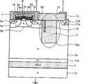
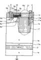
图49是表示使用现有的膜厚SOI基板制作的IGBT的截面结构的图。如图49所示,SOI基板是在支撑基板101上隔着绝缘层102层叠有作为活性层的电阻率高的n-漂移区域103的结构。Fig. 49 is a diagram showing a cross-sectional structure of an IGBT fabricated using a conventional thick-film SOI substrate. As shown in FIG. 49 , the SOI substrate has a structure in which an n− drift region 103 having a high resistivity as an active layer is stacked on a supporting
在n-漂移区域103的表面层的一部分,设置有p基极区域104。A
在p基极区域104的表面层的一部分,设置有n+发射极区域106和与此相接的p+低电阻区域105。该p+低电阻区域105的一部分占据n+发射极区域106的下面的部分。In a part of the surface layer of the
此外,在n-漂移区域103的表面层的一部分,与p基极区域104分离设置有n缓冲区域111。n缓冲区域111的电阻率比n-漂移区域103的电阻率低。在该n缓冲区域111的表面层的一部分,设置有p+集电极区域112。In addition, ann
发射极电极107与p+低电阻区域105和n+发射极区域106这两者接触。在n-漂移区域103和n+发射极区域106所夹着的p基极区域104的表面上,隔着绝缘膜109设置有栅极电极108。集电极电极110与p+集电极区域112接触。
在图49所示结构的IGBT中,通过p+集电极区域112、由n缓冲区域111与n-漂移区域103构成的n区域、由p基极区域104与p+低电阻区域105构成的p区域,构成PNP双极晶体管。此外,通过n+发射极区域106、p基极区域104和n-漂移区域103构成NPN双极晶体管。In theIGBT with thestructure shown in FIG. region, forming a PNP bipolar transistor. Furthermore, an NPN bipolar transistor is formed by the n+ emitter region 106 , the
并且,通过这些PNP双极晶体管和NPN双极晶体管,构成寄生半导体开关元件。为了避免由该寄生半导体开关元件引起的闭锁,设定导通电流的上限。为了使导通电流的上限值提高,只要使上述NPN双极晶体管不动作即可。And, these PNP bipolar transistors and NPN bipolar transistors constitute parasitic semiconductor switching elements. In order to avoid latch-up caused by this parasitic semiconductor switching element, an upper limit of ON current is set. In order to increase the upper limit value of the conduction current, it is only necessary to disable the above-mentioned NPN bipolar transistor.
为此,需要将从沟道端侧通过n+发射极区域106的下面到达p+低电阻区域105的电流通路的电阻抑制得较低。关于此,公知的方法是通过离子注入使上述电流通路的电阻下降。此外,还公知当形成p+低电阻区域105时通过掩膜匹配除去不确定性,使上述电流通路的长度为最小限度,形成能够获得与栅极电极的自我匹配的沟槽发射极电极的方法。For this reason, the resistance of the current path from the channel end side to the p+ low-
而且,还公知当元件为导通状态时,使从p+集电极区域112流入n-漂移区域103的载流子的一部分,不通过上述电流通路而到达p+低电阻区域105的结构。此外,在如图49所示结构的IGBT中,电场集中在n-漂移区域103与p基极区域104的晶片表面附近的界面、以及n-漂移区域103与n缓冲区域111的晶片表面附近的界面。Furthermore, a structure is known in which a part of carriers flowing from p+ collector region 112 into n− drift region 103 reaches p+
为了缓和该电场的集中,作为场电极(field plate),有使发射极电极107和集电极电极110隔着绝缘膜109以覆盖所述界面的方式延伸的情况。作为需要更加高的耐压的情况下、或者在漂移区域上存在电源线等配线的情况下的结构,公知的是在晶片表面的漂移区域的上面或者漂移区域的内部,设置有电容耦合型的场电极的结构。In order to alleviate the concentration of the electric field, the
在以上这种现有的将MOS晶体管和双极晶体管复合的设备中,为了在沿着晶片表面的方向上维持电压,单位设备的尺寸与设计耐压值的比例变大。因此,在高耐压且大电流用途的设备中,存在芯片面积变大的缺点。In the above conventional devices combining MOS transistors and bipolar transistors, in order to maintain voltage along the wafer surface, the ratio of the size of the unit device to the design withstand voltage value becomes large. Therefore, there is a disadvantage that the chip area becomes larger in devices for high withstand voltage and high current applications.
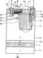
因此,在横型MOS晶体管中,为了减少在晶片表面所占的漂移区域的面积,提出有在漂移区域形成沟槽,以破坏电场比硅大的氧化硅膜埋入该沟槽的结构(例如,参照专利文献1)。根据该提案,如图50所示,实效的漂移长度Leff为从形成沟道的p阱区204与作为漂移区域的n阱区203的边界到沟槽内埋入的氧化膜217为止的距离LP、沟槽深度LT、沟槽宽度LB和再一个沟槽深度LT相加的长度。Therefore, in a lateral MOS transistor, in order to reduce the area of the drift region occupied on the wafer surface, it has been proposed to form a trench in the drift region and to bury a silicon oxide film having a destruction electric field larger than that of silicon into the trench (for example, Refer to Patent Document 1). According to this proposal, as shown in FIG. 50 , the effective drift length Leff is the distance from the boundary between the p-well region 204 forming the channel and the n-well region 203 as the drift region to the oxide film 217 buried in the trench. The sum of LP , groove depth LT , groove width LB and another groove depth LT .
另一方面,从晶片表面上的p阱区204与n阱区203的边界到漂移区域212为止的距离LD是LP和LB相加的长度。因此,能够使Leff比未设置埋入氧化膜217的情况长,所以与相同耐压的设备相比较,导通电阻RonA降低。在此,Ron为每单位面积的导通电阻,A是表面积。换言之,能够得到具有与现有相同的耐压和导通电流,并且比现有的设备间距小的横型设备。On the other hand, the distance LD from the boundary between p-well region 204 and n-well region 203on the wafer surface to drift region 212 is the sum ofLP andLB. Therefore, since Leff can be made longer than the case where the buried oxide film 217 is not provided, the on-resistance Ron A is lowered compared with a device having the same breakdown voltage. Here, Ron is the on-resistance per unit area, and A is the surface area. In other words, it is possible to obtain a horizontal device having the same withstand voltage and conduction current as conventional devices and having a smaller pitch than conventional devices.
此外,提出有在具有SOI(硅·导通·绝缘体)结构的横型IGBT中,在n型活性层上形成沟槽,并且在该沟槽的下面局部地设置高浓度的n型迂回(bypass)层的结构(例如,参照专利文献2)。根据该提案,流入源极电极的空穴电流通过沟槽降低,并且电子电流通过迂回层流通,所以源极侧的电子电流的累积增加,导通电压降低。In addition, it has been proposed to form a trench on the n-type active layer in a lateral IGBT having an SOI (silicon-on-insulator) structure, and to locally provide a high-concentration n-type bypass under the trench. Layer structure (for example, refer to Patent Document 2). According to this proposal, the hole current flowing into the source electrode is reduced through the trench, and the electron current flows through the detour layer, so the accumulation of the electron current on the source side increases, and the on-state voltage decreases.
但是,在上述专利文献2中公开的结构的IGBT中,具有如下所述的各种问题。即,例如当SOI结构通过贴合晶片实现的情况下,需要以迂回层位于沟槽的正下方的方式,以μm级别的位置对准精度贴合两枚晶片,在制造上并不优选。此外,在专利文献2的图2或者图3所示的布局中,通过晶片表面的n型活性层的长度决定耐压,因此不能缩短设备的单元间距。因此,不能降低每单位面积的导通电阻。However, the IGBT having the structure disclosed in
此外,在专利文献2的图4所示的布局,并且具有如图8所示的截面结构的情况下,由于在沟槽的周围存在低电阻区域,因此耐压由除去沟槽的晶片表面的n型活性层的长度决定。因此,不能缩短设备的单元间距,不能降低每单位面积的导通电阻。In addition, in the case of the layout shown in FIG. 4 of
此外,在专利文献2的图4所示的布局,并且具有如图6所示的截面结构的设备中,由于未在沟槽17下形成空穴的通路,所以栅极侧的电导度(conductivity)调制消失损害IGBT的优点。此外,为了保持栅极侧的电导度调制,若为该公报的图2所示的布局时,由于设备间距由表面漂移区域3的长度决定所以不能缩短间距。In addition, in the device with the layout shown in FIG. 4 of
进一步,在专利文献2的图5所示的截面结构中,由于沟槽底和迂回层之间的活性层的距离由离子注入能量决定,所以不能使该部分加厚,限制与耐压的权衡(tradeoff)。Furthermore, in the cross-sectional structure shown in FIG. 5 of
本发明为了解决上述的现有技术的问题点,所以其目的在于提供能够实现高耐压且大电流的驱动,并且闭锁容量高,每单位面积的导通电阻低的横型的IGBT。In order to solve the above-mentioned problems of the prior art, an object of the present invention is to provide a horizontal IGBT capable of high withstand voltage and large current drive, high latch capacity, and low on-resistance per unit area.
专利文献1:日本专利特开平8-97411号公报Patent Document 1: Japanese Patent Laid-Open No. 8-97411
专利文献2:日本专利特开平8-88357号公报(图1~图8)Patent Document 2: Japanese Patent Application Laid-Open No. 8-88357 (FIGS. 1 to 8)
发明内容Contents of the invention
为了解决上述课题,达成目的,第1方面的发明的SOI沟槽横型IGBT,其特征在于,包括:在支撑基板上隔着绝缘层设置的第一导电型的半导体层;设置在上述半导体层上、比上述半导体层电阻率高的第一导电型的第一半导体区域;设置在上述第一半导体区域的表面层的一部分、比上述第一半导体区域电阻率低的第一导电型的第二半导体区域;与上述第一半导体区域和上述第二半导体区域连接且设置于上述第一半导体区域的表面层的一部分的第二导电型的第三半导体区域;在上述第三半导体区域的一部分的表面上隔着栅极绝缘膜设置的栅极电极;设置于上述第三半导体区域的一部分的第一导电型的发射极区域;设置于上述第三半导体区域的一部分,并且设置在上述发射极区域的下侧的第二导电型的低电阻区域;在上述第三半导体区域的一部分上、与上述发射极区域邻接设置的第二导电型的高电导度区域;在上述第一半导体区域的表面层的一部分上、与上述第二半导体区域和上述第三半导体区域分离设置的、比上述第一半导体区域电阻率低的第一导电型的第四半导体区域;设置于上述第四半导体区域的一部分的第二导电型的集电极区域;设置在上述第二半导体区域和上述第三半导体区域与上述第四半导体区域之间的上层沟槽;从上述上层沟槽的底向更深位置设置的、比上述上层沟槽的宽度窄的下层沟槽;埋入在上述上层沟槽和上述下层沟槽中的埋入沟槽绝缘膜;埋入在上述上层沟槽内的上述埋入沟槽绝缘膜中的、在上述第三半导体区域的附近的漂移电位的发射极侧导电区域;埋入在上述上层沟槽内的上述埋入沟槽绝缘膜中的、在上述第四半导体区域的附近的集电极侧导电区域;与上述发射极区域和上述高电导度区域连接的发射极电极;和与上述集电极区域连接,并且与上述集电极侧导电区域电连接的集电极电极。In order to solve the above-mentioned problems and achieve the purpose, the SOI trench lateral IGBT according to the first aspect of the invention is characterized in that it includes: a semiconductor layer of the first conductivity type provided on the support substrate through an insulating layer; provided on the above-mentioned semiconductor layer A first semiconductor region of the first conductivity type having a higher resistivity than the above-mentioned semiconductor layer; a second semiconductor of the first conductivity type having a resistivity lower than that of the first semiconductor region provided on a part of the surface layer of the first semiconductor region a region; a third semiconductor region of the second conductivity type connected to the first semiconductor region and the second semiconductor region and provided on a part of the surface layer of the first semiconductor region; on a part of the surface of the third semiconductor region A gate electrode provided through a gate insulating film; a first conductivity type emitter region provided in a part of the third semiconductor region; a part of the third semiconductor region provided under the emitter region A low-resistance region of the second conductivity type on the side; a high-conductivity region of the second conductivity type adjacent to the emitter region on a part of the third semiconductor region; a part of the surface layer of the first semiconductor region A fourth semiconductor region of the first conductivity type, which is separated from the second semiconductor region and the third semiconductor region and has a lower resistivity than the first semiconductor region; the second semiconductor region arranged in a part of the fourth semiconductor region The collector region of the conductivity type; the upper layer trench arranged between the above-mentioned second semiconductor region, the above-mentioned third semiconductor region and the above-mentioned fourth semiconductor region; a lower trench with a narrow groove width; a buried trench insulating film buried in the upper trench and the lower trench; a buried trench insulating film buried in the upper trench, An emitter-side conductive region of drift potential in the vicinity of the third semiconductor region; a collector-side conductive region buried in the buried trench insulating film in the upper trench and in the vicinity of the fourth semiconductor region an emitter electrode connected to the emitter region and the high-conductivity region; and a collector electrode connected to the collector region and electrically connected to the collector-side conductive region.
第2方面的发明的SOI沟槽横型IGBT,其特征在于,包括:在支撑基板上隔着绝缘层设置的第一导电型的半导体层;设置在上述半导体层上、比上述半导体层电阻率高的第一导电型的第一半导体区域;设置在上述第一半导体区域的表面层的一部分、比上述第一半导体区域电阻率低的第一导电型的第二半导体区域;与上述第一半导体区域和上述第二半导体区域连接且设置于上述第一半导体区域的表面层的一部分的第二导电型的第三半导体区域;在上述第三半导体区域的一部分的表面上隔着栅极绝缘膜设置的栅极电极;设置于上述第三半导体区域的一部分的第一导电型的发射极区域;设置于上述第三半导体区域的一部分,并且设置在上述发射极区域的下侧的第二导电型的低电阻区域;在上述第三半导体区域的一部分上、与上述发射极区域邻接设置的第二导电型的高电导度区域;在上述第一半导体区域的表面层的一部分上、与上述第二半导体区域和上述第三半导体区域分离设置的、比上述第一半导体区域电阻率低的第一导电型的第四半导体区域;设置于上述第四半导体区域的一部分的第二导电型的集电极区域;设置在上述第二半导体区域和上述第三半导体区域与上述第四半导体区域之间的沟槽;埋入在上述沟槽内的埋入沟槽绝缘膜;埋入上述埋入沟槽绝缘膜的上半部内的、在上述第三半导体区域的附近的漂移电位的发射极侧导电区域;埋入上述埋入沟槽绝缘膜的上半部内的、在上述第四半导体区域的附近的集电极侧导电区域;与上述发射极区域和上述高电导度区域连接的发射极电极;和与上述集电极区域连接,并且与上述集电极侧导电区域电连接的集电极电极。The SOI trench lateral IGBT of the invention according to claim 2 is characterized by comprising: a first conductivity type semiconductor layer provided on a support substrate via an insulating layer; a first semiconductor region of the first conductivity type; a second semiconductor region of the first conductivity type which is provided on a part of the surface layer of the first semiconductor region and has a lower resistivity than the first semiconductor region; and the first semiconductor region A third semiconductor region of the second conductivity type connected to the second semiconductor region and provided on a part of the surface layer of the first semiconductor region; a part of the surface of the third semiconductor region provided via a gate insulating film A gate electrode; an emitter region of the first conductivity type provided on a part of the third semiconductor region; a low electrode region of the second conductivity type provided on a part of the third semiconductor region and below the emitter region A resistance region; a second conductivity type high-conductivity region disposed adjacent to the emitter region on a part of the third semiconductor region; a part of the surface layer of the first semiconductor region, adjacent to the second semiconductor region A fourth semiconductor region of the first conductivity type, which is separated from the third semiconductor region and has a lower resistivity than the first semiconductor region; a collector region of the second conductivity type arranged in a part of the fourth semiconductor region; The trench between the second semiconductor region, the third semiconductor region, and the fourth semiconductor region; the buried trench insulating film buried in the trench; the buried trench insulating film buried above the The emitter side conductive region of the drift potential in the vicinity of the third semiconductor region in the half; the collector side conductive region in the vicinity of the fourth semiconductor region buried in the upper half of the buried trench insulating film region; an emitter electrode connected to the emitter region and the high-conductivity region; and a collector electrode connected to the collector region and electrically connected to the collector-side conductive region.
第3方面的发明的SOI沟槽横型IGBT,其特征在于,包括:在支撑基板上隔着绝缘层设置的第一导电型的半导体层;设置在上述半导体层上、比上述半导体层电阻率高的第一导电型的第一半导体区域;与上述第一半导体区域连接,并且设置于上述第一半导体区域的表面层的一部分的第二导电型的第三半导体区域;在贯通上述第三半导体区域并到达上述第一半导体区域的栅极沟槽的内侧隔着栅极绝缘膜设置的栅极电极;在上述第三半导体区域的一部分上、与上述栅极沟槽连接设置的第一导电型的发射极区域;在上述第三半导体区域的一部分上、与上述发射极区域邻接设置的第二导电型的低电阻区域;在上述第一半导体区域的表面层的一部分上、与上述第三半导体区域分离设置的、比上述第一半导体区域电阻率低的第一导电型的第四半导体区域;设置于上述第四半导体区域的一部分的第二导电型的集电极区域;设置在上述第三半导体区域与上述第四半导体区域之间的上层沟槽;从上述上层沟槽的底向更深位置设置的、比上述上层沟槽的宽度窄的下层沟槽;埋入在上述上层沟槽和上述下层沟槽中的埋入沟槽绝缘膜;埋入上述上层沟槽内的上述埋入沟槽绝缘膜中的、在上述第三半导体区域的附近的漂移电位的发射极侧导电区域;埋入上述上层沟槽内的上述埋入沟槽绝缘膜中的、在上述第四半导体区域的附近的集电极侧导电区域;与上述发射极区域和上述低电阻区域连接的发射极电极;和与上述集电极区域连接,并且与上述集电极侧导电区域电连接的集电极电极。The SOI trench lateral IGBT of the invention according to claim 3 is characterized by comprising: a first conductivity type semiconductor layer provided on the support substrate via an insulating layer; A first semiconductor region of the first conductivity type; a third semiconductor region of the second conductivity type connected to the first semiconductor region and provided on a part of the surface layer of the first semiconductor region; and reach the inner side of the gate trench of the first semiconductor region through the gate electrode provided through the gate insulating film; an emitter region; a low-resistance region of the second conductivity type disposed adjacent to the emitter region on a part of the third semiconductor region; a part of the surface layer of the first semiconductor region, adjacent to the third semiconductor region A fourth semiconductor region of the first conductivity type that is separately disposed and has a lower resistivity than the first semiconductor region; a collector region of the second conductivity type disposed in a part of the fourth semiconductor region; disposed in the third semiconductor region The upper layer trench between the above-mentioned fourth semiconductor region; the lower layer trench arranged from the bottom of the above-mentioned upper layer trench to a deeper position and narrower than the width of the above-mentioned upper layer trench; buried in the above-mentioned upper layer trench and the above-mentioned lower layer trench A buried trench insulating film in the trench; an emitter-side conductive region of drift potential in the vicinity of the third semiconductor region buried in the buried trench insulating film in the trench of the upper layer; buried in the upper layer The collector-side conductive region in the vicinity of the fourth semiconductor region buried in the trench insulating film in the trench; the emitter electrode connected to the emitter region and the low-resistance region; and the collector electrode The region is connected and electrically connected to the collector electrode on the collector side conductive region.
第4方面的发明的SOI沟槽横型IGBT,其特征在于,包括:在支撑基板上隔着绝缘层设置的第一导电型的半导体层;设置在上述半导体层上、比上述半导体层电阻率高的第一导电型的第一半导体区域;与上述第一半导体区域连接,并且设置于上述第一半导体区域的表面层的一部分的第二导电型的第三半导体区域;在贯通上述第三半导体区域并到达上述第一半导体区域的栅极沟槽的内侧隔着栅极绝缘膜设置的栅极电极;在上述第三半导体区域的一部分上、与上述栅极沟槽连接设置的第一导电型的发射极区域;在上述第三半导体区域的一部分上、与上述发射极区域邻接设置的第二导电型的低电阻区域;在上述第一半导体区域的表面层的一部分上、与上述第三半导体区域分离设置的、比上述第一半导体区域电阻率低的第一导电型的第四半导体区域;设置于上述第四半导体区域的一部分的第二导电型的集电极区域;设置在上述第三半导体区域与上述第四半导体区域之间的沟槽;埋入在上述沟槽内的埋入沟槽绝缘膜;埋入上述埋入沟槽绝缘膜的上半部内的、在上述第三半导体区域的附近的漂移电位的发射极侧导电区域;埋入上述埋入沟槽绝缘膜的上半部内的、在上述第四半导体区域的附近的集电极侧导电区域;与上述发射极区域和上述低电阻区域连接的发射极电极;和与上述集电极区域连接,并且与上述集电极侧导电区域电连接的集电极电极。The SOI trench lateral IGBT according to the fourth aspect of the invention is characterized by comprising: a semiconductor layer of the first conductivity type provided on the support substrate via an insulating layer; A first semiconductor region of the first conductivity type; a third semiconductor region of the second conductivity type connected to the first semiconductor region and provided on a part of the surface layer of the first semiconductor region; and reach the inner side of the gate trench of the first semiconductor region through the gate electrode provided through the gate insulating film; an emitter region; a low-resistance region of the second conductivity type disposed adjacent to the emitter region on a part of the third semiconductor region; a part of the surface layer of the first semiconductor region, adjacent to the third semiconductor region A fourth semiconductor region of the first conductivity type that is separately disposed and has a lower resistivity than the first semiconductor region; a collector region of the second conductivity type disposed in a part of the fourth semiconductor region; disposed in the third semiconductor region A trench between the above-mentioned fourth semiconductor region; a buried trench insulating film buried in the above-mentioned trench; a buried trench insulating film buried in the upper half of the above-mentioned third semiconductor region The emitter-side conductive region of the drift potential; the collector-side conductive region buried in the upper half of the buried trench insulating film in the vicinity of the above-mentioned fourth semiconductor region; and the above-mentioned emitter region and the above-mentioned low-resistance region an emitter electrode connected; and a collector electrode connected to the collector region and electrically connected to the collector-side conductive region.
第5方面的发明的SOI沟槽横型IGBT,其特征在于,包括:在支撑基板上隔着绝缘层设置的第一导电型的半导体层;设置在上述半导体层上、比上述半导体层电阻率高的第一导电型的第一半导体区域;设置在上述第一半导体区域的表面层的一部分、比上述第一半导体区域电阻率低的第一导电型的第二半导体区域;与上述第一半导体区域和上述第二半导体区域连接且设置于上述第一半导体区域的表面层的一部分的第二导电型的第三半导体区域;在上述第三半导体区域的一部分的表面上隔着栅极绝缘膜设置的栅极电极;设置于上述第三半导体区域的一部分的第一导电型的发射极区域;设置于上述第三半导体区域的一部分,并且设置在上述发射极区域的下侧的第二导电型的低电阻区域;在上述第三半导体区域的一部分上、与上述发射极区域邻接设置的第二导电型的高电导度区域;在上述第一半导体区域的表面层的一部分上、与上述第二半导体区域和上述第三半导体区域分离设置的、比上述第一半导体区域电阻率低的第一导电型的第四半导体区域;设置于上述第四半导体区域的一部分的第二导电型的集电极区域;在上述第二半导体区域和上述第三半导体区域与上述第四半导体区域之间、与上述第四半导体区域分离设置的上层沟槽;从上述上层沟槽的底向更深位置设置的、比上述上层沟槽的宽度窄的下层沟槽;埋入在上述上层沟槽和上述下层沟槽中的埋入沟槽绝缘膜;埋入上述上层沟槽内的上述埋入沟槽绝缘膜中的、在上述第三半导体区域的附近的漂移电位的发射极侧导电区域;与上述发射极区域和上述高电导度区域连接的发射极电极;和与上述集电极区域连接的集电极电极。The SOI trench lateral IGBT according to the fifth aspect of the invention is characterized by comprising: a semiconductor layer of the first conductivity type provided on the support substrate via an insulating layer; and a semiconductor layer provided on the semiconductor layer having a higher resistivity than the semiconductor layer a first semiconductor region of the first conductivity type; a second semiconductor region of the first conductivity type which is provided on a part of the surface layer of the first semiconductor region and has a lower resistivity than the first semiconductor region; and the first semiconductor region A third semiconductor region of the second conductivity type connected to the second semiconductor region and provided on a part of the surface layer of the first semiconductor region; a part of the surface of the third semiconductor region provided via a gate insulating film A gate electrode; an emitter region of the first conductivity type provided on a part of the third semiconductor region; a low electrode region of the second conductivity type provided on a part of the third semiconductor region and below the emitter region A resistance region; a second conductivity type high-conductivity region disposed adjacent to the emitter region on a part of the third semiconductor region; a part of the surface layer of the first semiconductor region, adjacent to the second semiconductor region A fourth semiconductor region of the first conductivity type, which is separated from the third semiconductor region and has a lower resistivity than the first semiconductor region; a collector region of the second conductivity type provided in a part of the fourth semiconductor region; The upper trench between the above-mentioned second semiconductor region, the above-mentioned third semiconductor region, and the above-mentioned fourth semiconductor region, which is separated from the above-mentioned fourth semiconductor region; The lower trench with a narrow groove width; the buried trench insulating film buried in the above-mentioned upper trench and the above-mentioned lower trench; the buried trench insulating film buried in the above-mentioned upper trench, in the above-mentioned an emitter-side conductive region of drift potential near the third semiconductor region; an emitter electrode connected to the emitter region and the high-conductivity region; and a collector electrode connected to the collector region.
第6方面的发明的SOI沟槽横型IGBT,其特征在于,包括:在支撑基板上隔着绝缘层设置的第一导电型的半导体层;设置在上述半导体层上、比上述半导体层电阻率高的第一导电型的第一半导体区域;设置在上述第一半导体区域的表面层的一部分、比上述第一半导体区域电阻率低的第一导电型的第二半导体区域;与上述第一半导体区域和上述第二半导体区域连接且设置于上述第一半导体区域的表面层的一部分的第二导电型的第三半导体区域;在上述第三半导体区域的一部分的表面上隔着栅极绝缘膜设置的栅极电极;设置于上述第三半导体区域的一部分的第一导电型的发射极区域;设置于上述第三半导体区域的一部分,并且设置在上述发射极区域的下侧的第二导电型的低电阻区域;在上述第三半导体区域的一部分上、与上述发射极区域邻接设置的第二导电型的高电导度区域;在上述第一半导体区域的表面层的一部分上、与上述第二半导体区域和上述第三半导体区域分离设置的、比上述第一半导体区域电阻率低的第一导电型的第四半导体区域;设置于上述第四半导体区域的一部分的第二导电型的集电极区域;在上述第二半导体区域和上述第三半导体区域与上述第四半导体区域之间、与上述第四半导体区域分离设置的沟槽;埋入在上述沟槽内的埋入沟槽绝缘膜;埋入上述埋入沟槽绝缘膜的上半部内的、在上述第三半导体区域的附近的漂移电位的发射极侧导电区域;与上述发射极区域和上述高电导度区域连接的发射极电极;和与上述集电极区域连接的集电极电极。The SOI trench lateral IGBT according to the sixth aspect of the invention is characterized by comprising: a semiconductor layer of the first conductivity type provided on the support substrate via an insulating layer; a first semiconductor region of the first conductivity type; a second semiconductor region of the first conductivity type which is provided on a part of the surface layer of the first semiconductor region and has a lower resistivity than the first semiconductor region; and the first semiconductor region A third semiconductor region of the second conductivity type connected to the second semiconductor region and provided on a part of the surface layer of the first semiconductor region; a part of the surface of the third semiconductor region provided via a gate insulating film A gate electrode; an emitter region of the first conductivity type provided on a part of the third semiconductor region; a low electrode region of the second conductivity type provided on a part of the third semiconductor region and below the emitter region A resistance region; a second conductivity type high-conductivity region disposed adjacent to the emitter region on a part of the third semiconductor region; a part of the surface layer of the first semiconductor region, adjacent to the second semiconductor region A fourth semiconductor region of the first conductivity type, which is separated from the third semiconductor region and has a lower resistivity than the first semiconductor region; a collector region of the second conductivity type provided in a part of the fourth semiconductor region; A trench separated from the fourth semiconductor region between the second semiconductor region, the third semiconductor region, and the fourth semiconductor region; a buried trench insulating film buried in the trench; an emitter-side conductive region of drift potential in the vicinity of the above-mentioned third semiconductor region buried in the upper half of the trench insulating film; an emitter electrode connected to the above-mentioned emitter region and the above-mentioned high-conductivity region; and the above-mentioned The collector electrode to which the collector region is connected.
第7方面的发明的SOI沟槽横型IGBT,其特征在于,包括:在支撑基板上隔着绝缘层设置的第一导电型的半导体层;设置在上述半导体层上、比上述半导体层电阻率高的第一导电型的第一半导体区域;与上述第一半导体区域连接,并且设置于上述第一半导体区域的表面层的一部分的第二导电型的第三半导体区域;在贯通上述第三半导体区域并到达上述第一半导体区域的栅极沟槽的内侧隔着栅极绝缘膜设置的栅极电极;在上述第三半导体区域的一部分上、与上述栅极沟槽连接设置的第一导电型的发射极区域;在上述第三半导体区域的一部分上、与上述发射极区域邻接设置的第二导电型的低电阻区域;在上述第一半导体区域的表面层的一部分上、与上述第三半导体区域分离设置的、比上述第一半导体区域电阻率低的第一导电型的第四半导体区域;设置于上述第四半导体区域的一部分的第二导电型的集电极区域;在上述第三半导体区域与上述第四半导体区域之间、与上述第四半导体区域分离设置的上层沟槽;从上述上层沟槽的底向更深位置设置的、比上述上层沟槽的宽度窄的下层沟槽;埋入在上述上层沟槽和上述下层沟槽中的埋入沟槽绝缘膜;埋入上述上层沟槽内的上述埋入沟槽绝缘膜中的、在上述第三半导体区域的附近的漂移电位的发射极侧导电区域;与上述发射极区域和上述低电阻区域连接的发射极电极;和与上述集电极区域连接的集电极电极。The SOI trench lateral IGBT according to the seventh aspect of the invention is characterized by comprising: a semiconductor layer of the first conductivity type provided on the support substrate via an insulating layer; A first semiconductor region of the first conductivity type; a third semiconductor region of the second conductivity type connected to the first semiconductor region and provided on a part of the surface layer of the first semiconductor region; and reach the inner side of the gate trench of the first semiconductor region through the gate electrode provided through the gate insulating film; an emitter region; a low-resistance region of the second conductivity type disposed adjacent to the emitter region on a part of the third semiconductor region; a part of the surface layer of the first semiconductor region, adjacent to the third semiconductor region A fourth semiconductor region of the first conductivity type that is separately disposed and has a lower resistivity than the first semiconductor region; a collector region of the second conductivity type that is disposed on a part of the fourth semiconductor region; and between the third semiconductor region and the An upper layer trench between the above-mentioned fourth semiconductor regions and separated from the above-mentioned fourth semiconductor region; a lower layer trench arranged from the bottom of the above-mentioned upper layer trench to a deeper position and narrower than the width of the above-mentioned upper layer trench; The buried trench insulating film in the upper trench and the lower trench; the emitter of the drift potential in the vicinity of the third semiconductor region buried in the buried trench insulating film in the upper trench a side conductive region; an emitter electrode connected to the aforementioned emitter region and the aforementioned low resistance region; and a collector electrode connected to the aforementioned collector region.
第8方面的发明的SOI沟槽横型IGBT,其特征在于,包括:在支撑基板上隔着绝缘层设置的第一导电型的半导体层;设置在上述半导体层上、比上述半导体层电阻率高的第一导电型的第一半导体区域;与上述第一半导体区域连接,并且设置于上述第一半导体区域的表面层的一部分的第二导电型的第三半导体区域;在贯通上述第三半导体区域并到达上述第一半导体区域的栅极沟槽的内侧隔着栅极绝缘膜设置的栅极电极;在上述第三半导体区域的一部分上、与上述栅极沟槽连接设置的第一导电型的发射极区域;在上述第三半导体区域的一部分上、与上述发射极区域邻接设置的第二导电型的低电阻区域;在上述第一半导体区域的表面层的一部分上、与上述第三半导体区域分离设置的、比上述第一半导体区域电阻率低的第一导电型的第四半导体区域;设置于上述第四半导体区域的一部分的第二导电型的集电极区域;在上述第三半导体区域与上述第四半导体区域之间、与上述第四半导体区域分离设置的沟槽;埋入在上述沟槽内的埋入沟槽绝缘膜;埋入上述埋入沟槽绝缘膜的上半部内的、在上述第三半导体区域的附近的漂移电位的发射极侧导电区域;与上述发射极区域和上述低电阻区域连接的发射极电极;和与上述集电极区域连接的集电极电极。The SOI trench lateral IGBT according to the eighth invention is characterized by comprising: a semiconductor layer of the first conductivity type provided on the support substrate via an insulating layer; and a semiconductor layer provided on the semiconductor layer and having a higher resistivity than the semiconductor layer A first semiconductor region of the first conductivity type; a third semiconductor region of the second conductivity type connected to the first semiconductor region and provided on a part of the surface layer of the first semiconductor region; and reach the inner side of the gate trench of the first semiconductor region through the gate electrode provided through the gate insulating film; an emitter region; a low-resistance region of the second conductivity type disposed adjacent to the emitter region on a part of the third semiconductor region; a part of the surface layer of the first semiconductor region, adjacent to the third semiconductor region A fourth semiconductor region of the first conductivity type that is separately disposed and has a lower resistivity than the first semiconductor region; a collector region of the second conductivity type that is disposed on a part of the fourth semiconductor region; and between the third semiconductor region and the A trench provided between the fourth semiconductor regions and separated from the fourth semiconductor region; a buried trench insulating film buried in the trench; a buried trench insulating film buried in the upper half of the buried trench insulating film, an emitter-side conductive region of drift potential in the vicinity of the third semiconductor region; an emitter electrode connected to the emitter region and the low-resistance region; and a collector electrode connected to the collector region.
第9方面的发明的SOI沟槽横型IGBT,其特征在于,包括:在支撑基板上隔着绝缘层设置的第一导电型的半导体层;设置在上述半导体层上、比上述半导体层电阻率高的第一导电型的第一半导体区域;设置在上述第一半导体区域的表面层的一部分、比上述第一半导体区域电阻率低的第一导电型的第二半导体区域;与上述第一半导体区域和上述第二半导体区域连接且设置于上述第一半导体区域的表面层的一部分的第二导电型的第三半导体区域;在上述第三半导体区域的一部分的表面上隔着栅极绝缘膜设置的栅极电极;设置于上述第三半导体区域的一部分的第一导电型的发射极区域;设置于上述第三半导体区域的一部分,并且设置在上述发射极区域的下侧的第二导电型的低电阻区域;在上述第三半导体区域的一部分上、与上述发射极区域邻接设置的第二导电型的高电导度区域;在上述第一半导体区域的表面层的一部分上、与上述第二半导体区域和上述第三半导体区域分离设置的、比上述第一半导体区域电阻率低的第一导电型的第四半导体区域;设置于上述第四半导体区域的一部分的第二导电型的集电极区域;在上述第二半导体区域和上述第三半导体区域与上述第四半导体区域之间、与上述第三半导体区域分离设置的上层沟槽;从上述上层沟槽的底向更深位置设置的、比上述上层沟槽的宽度窄的下层沟槽;埋入在上述上层沟槽和上述下层沟槽中的埋入沟槽绝缘膜;埋入上述上层沟槽内的上述埋入沟槽绝缘膜中的、在上述第四半导体区域的附近的集电极侧导电区域;与上述发射极区域和上述高电导度区域连接的发射极电极;和与上述集电极区域连接,并且与上述集电极侧导电区域电连接的集电极电极。The SOI trench lateral IGBT according to the ninth aspect of the invention is characterized by comprising: a semiconductor layer of the first conductivity type provided on the support substrate via an insulating layer; a first semiconductor region of the first conductivity type; a second semiconductor region of the first conductivity type which is provided on a part of the surface layer of the first semiconductor region and has a lower resistivity than the first semiconductor region; and the first semiconductor region A third semiconductor region of the second conductivity type connected to the second semiconductor region and provided on a part of the surface layer of the first semiconductor region; a part of the surface of the third semiconductor region provided via a gate insulating film A gate electrode; an emitter region of the first conductivity type provided on a part of the third semiconductor region; a low electrode region of the second conductivity type provided on a part of the third semiconductor region and below the emitter region A resistance region; a second conductivity type high-conductivity region disposed adjacent to the emitter region on a part of the third semiconductor region; a part of the surface layer of the first semiconductor region, adjacent to the second semiconductor region A fourth semiconductor region of the first conductivity type, which is separated from the third semiconductor region and has a lower resistivity than the first semiconductor region; a collector region of the second conductivity type provided in a part of the fourth semiconductor region; The upper trench between the above-mentioned second semiconductor region, the above-mentioned third semiconductor region, and the above-mentioned fourth semiconductor region, which is separated from the above-mentioned third semiconductor region; The lower trench with a narrow groove width; the buried trench insulating film buried in the above-mentioned upper trench and the above-mentioned lower trench; the buried trench insulating film buried in the above-mentioned upper trench, in the above-mentioned a collector-side conductive region near the fourth semiconductor region; an emitter electrode connected to the emitter region and the high-conductivity region; and a collector connected to the collector region and electrically connected to the collector-side conductive region. electrode electrode.
第10方面的发明的SOI沟槽横型IGBT,其特征在于,包括:在支撑基板上隔着绝缘层设置的第一导电型的半导体层;设置在上述半导体层上、比上述半导体层电阻率高的第一导电型的第一半导体区域;设置在上述第一半导体区域的表面层的一部分、比上述第一半导体区域电阻率低的第一导电型的第二半导体区域;与上述第一半导体区域和上述第二半导体区域连接且设置于上述第一半导体区域的表面层的一部分的第二导电型的第三半导体区域;在上述第三半导体区域的一部分的表面上隔着栅极绝缘膜设置的栅极电极;设置于上述第三半导体区域的一部分的第一导电型的发射极区域;设置于上述第三半导体区域的一部分,并且设置在上述发射极区域的下侧的第二导电型的低电阻区域;在上述第三半导体区域的一部分上、与上述发射极区域邻接设置的第二导电型的高电导度区域;在上述第一半导体区域的表面层的一部分上、与上述第二半导体区域和上述第三半导体区域分离设置的、比上述第一半导体区域电阻率低的第一导电型的第四半导体区域;设置于上述第四半导体区域的一部分的第二导电型的集电极区域;在上述第二半导体区域和上述第三半导体区域与上述第四半导体区域之间、与上述第三半导体区域分离设置的沟槽;埋入在上述沟槽内的埋入沟槽绝缘膜;埋入上述埋入沟槽绝缘膜的上半部内的、在上述第四半导体区域的附近的集电极侧导电区域;与上述发射极区域和上述高电导度区域连接的发射极电极;和与上述集电极区域连接,并且与上述集电极侧导电区域电连接的集电极电极。The SOI trench lateral IGBT according to the tenth invention is characterized by comprising: a semiconductor layer of the first conductivity type provided on the support substrate via an insulating layer; a first semiconductor region of the first conductivity type; a second semiconductor region of the first conductivity type which is provided on a part of the surface layer of the first semiconductor region and has a lower resistivity than the first semiconductor region; and the first semiconductor region A third semiconductor region of the second conductivity type connected to the second semiconductor region and provided on a part of the surface layer of the first semiconductor region; a part of the surface of the third semiconductor region provided via a gate insulating film A gate electrode; an emitter region of the first conductivity type provided on a part of the third semiconductor region; a low electrode region of the second conductivity type provided on a part of the third semiconductor region and below the emitter region A resistance region; a second conductivity type high-conductivity region disposed adjacent to the emitter region on a part of the third semiconductor region; a part of the surface layer of the first semiconductor region, adjacent to the second semiconductor region A fourth semiconductor region of the first conductivity type, which is separated from the third semiconductor region and has a lower resistivity than the first semiconductor region; a collector region of the second conductivity type provided in a part of the fourth semiconductor region; A trench separated from the third semiconductor region between the second semiconductor region, the third semiconductor region, and the fourth semiconductor region; a buried trench insulating film buried in the trench; a collector-side conductive region buried in the upper half of the trench insulating film in the vicinity of the above-mentioned fourth semiconductor region; an emitter electrode connected to the above-mentioned emitter region and the above-mentioned high-conductivity region; and the above-mentioned collector region connected, and electrically connected to the collector electrode above the collector side conductive region.
第11方面的发明的SOI沟槽横型IGBT,其特征在于,包括:在支撑基板上隔着绝缘层设置的第一导电型的半导体层;设置在上述半导体层上、比上述半导体层电阻率高的第一导电型的第一半导体区域;设置在上述第一半导体区域的表面层的一部分、比上述第一半导体区域电阻率低的第一导电型的第二半导体区域;与上述第一半导体区域和上述第二半导体区域连接且设置于上述第一半导体区域的表面层的一部分的第二导电型的第三半导体区域;在上述第三半导体区域的一部分的表面上隔着栅极绝缘膜设置的栅极电极;设置于上述第三半导体区域的一部分的第一导电型的发射极区域;设置于上述第三半导体区域的一部分,并且设置在上述发射极区域的下侧的第二导电型的低电阻区域;在上述第三半导体区域的一部分上、与上述发射极区域邻接设置的第二导电型的高电导度区域;在上述第一半导体区域的表面层的一部分上、与上述第二半导体区域和上述第三半导体区域分离设置的、比上述第一半导体区域电阻率低的第一导电型的第四半导体区域;设置于上述第四半导体区域的一部分的第二导电型的集电极区域;在上述第二半导体区域和上述第三半导体区域与上述第四半导体区域之间、与上述第三半导体区域和上述第四半导体区域分离设置的沟槽;埋入在上述沟槽内的埋入沟槽绝缘膜;与上述发射极区域和上述高电导度区域连接的发射极电极;和与上述集电极区域连接的集电极电极。The SOI trench lateral IGBT according to the eleventh invention is characterized by comprising: a semiconductor layer of the first conductivity type provided on the supporting substrate via an insulating layer; and a semiconductor layer provided on the semiconductor layer having a higher resistivity than the semiconductor layer a first semiconductor region of the first conductivity type; a second semiconductor region of the first conductivity type which is provided on a part of the surface layer of the first semiconductor region and has a lower resistivity than the first semiconductor region; and the first semiconductor region A third semiconductor region of the second conductivity type connected to the second semiconductor region and provided on a part of the surface layer of the first semiconductor region; a part of the surface of the third semiconductor region provided via a gate insulating film A gate electrode; an emitter region of the first conductivity type provided on a part of the third semiconductor region; a low electrode region of the second conductivity type provided on a part of the third semiconductor region and below the emitter region A resistance region; a second conductivity type high-conductivity region disposed adjacent to the emitter region on a part of the third semiconductor region; a part of the surface layer of the first semiconductor region, adjacent to the second semiconductor region A fourth semiconductor region of the first conductivity type, which is separated from the third semiconductor region and has a lower resistivity than the first semiconductor region; a collector region of the second conductivity type provided in a part of the fourth semiconductor region; A trench provided between the second semiconductor region, the third semiconductor region, and the fourth semiconductor region and separated from the third semiconductor region and the fourth semiconductor region; a buried trench buried in the trench an insulating film; an emitter electrode connected to the above-mentioned emitter region and the above-mentioned high-conductivity region; and a collector electrode connected to the above-mentioned collector region.
第12方面的发明的SOI沟槽横型IGBT,其特征在于:在第1、2、5、6、9、10和11中任一方面所述的发明中,上述栅极绝缘膜、上述栅极电极、上述第三半导体区域、上述低电阻区域、上述发射极区域和上述高电导度区域,相对上述埋入沟槽绝缘膜在同一侧分别设置有多个,相邻的上述发射极区域和上述高电导度区域通过上述发射极电极相互电连接。The SOI trench lateral IGBT of the twelfth invention is characterized in that in any one of the
第13方面的发明的SOI沟槽横型IGBT,其特征在于:在第3、4、7和8中任一方面所述的发明中,上述栅极沟槽、上述栅极绝缘膜、上述栅极电极、上述第三半导体区域、上述低电阻区域和上述发射极区域,相对上述埋入沟槽绝缘膜在同一侧分别设置有多个,邻接的上述发射极区域和上述低电阻区域通过上述发射极电极相互电连接。The SOI trench lateral IGBT of the thirteenth invention is characterized in that in any one of the third, fourth, seventh and eighth inventions, the gate trench, the gate insulating film, the gate A plurality of electrodes, the third semiconductor region, the low-resistance region, and the emitter region are provided on the same side of the buried trench insulating film, and the adjacent emitter region and the low-resistance region pass through the emitter region. The electrodes are electrically connected to each other.
第14方面的发明的SOI沟槽横型IGBT,其特征在于:在第1~13中任一方面所述的发明中,上述支撑基板上的上述绝缘层与上述第一半导体区域之间的上述半导体层,具有对金属污染的消除效果。The SOI trench lateral IGBT according to the fourteenth invention is characterized in that in the invention according to any one of the first to the thirteenth invention, the semiconductor between the insulating layer and the first semiconductor region on the support substrate is characterized in that: layer, has the effect of eliminating metal pollution.
第15方面的发明的SOI沟槽横型IGBT,其特征在于,包括:在支撑基板上隔着绝缘层设置的第一导电型的半导体层;设置在上述半导体层上、比上述半导体层电阻率高的第一导电型的第一半导体区域;设置在上述第一半导体区域的表面层的一部分、比上述第一半导体区域电阻率低的第一导电型的第二半导体区域;与上述第一半导体区域和上述第二半导体区域连接且设置于上述第一半导体区域的表面层的一部分的第二导电型的第三半导体区域;设置于上述第三半导体区域的一部分的第一导电型的发射极区域;在上述第二半导体区域与上述发射极区域之间的上述第三半导体区域的表面上隔着栅极绝缘膜设置的栅极电极;在上述第一半导体区域的表面层的一部分上、与上述第二半导体区域和上述第三半导体区域分离设置的、比上述第一半导体区域电阻率低的第一导电型的第四半导体区域;设置于上述第四半导体区域的一部分的第二导电型的集电极区域;设置在上述第二半导体区域和上述第三半导体区域与上述第四半导体区域之间的沟槽;埋入在上述沟槽中的埋入沟槽绝缘膜;埋入上述沟槽内的上述埋入沟槽绝缘膜中的、在上述第三半导体区域与上述第一半导体区域的pn结的附近的漂移电位的发射极侧导电区域;埋入上述沟槽内的上述埋入沟槽绝缘膜中的、在上述第四半导体区域与上述第一半导体区域的界面的附近的集电极侧导电区域;与上述发射极区域连接的发射极电极;和与上述集电极区域连接,并且与上述集电极侧导电区域电连接的集电极电极。The SOI trench lateral IGBT according to the fifteenth invention is characterized by comprising: a semiconductor layer of the first conductivity type provided on the support substrate via an insulating layer; and a semiconductor layer provided on the semiconductor layer and having a higher resistivity than the semiconductor layer. a first semiconductor region of the first conductivity type; a second semiconductor region of the first conductivity type which is provided on a part of the surface layer of the first semiconductor region and has a lower resistivity than the first semiconductor region; and the first semiconductor region a third semiconductor region of the second conductivity type connected to the second semiconductor region and provided on a part of the surface layer of the first semiconductor region; an emitter region of the first conductivity type provided on a part of the third semiconductor region; A gate electrode provided on the surface of the third semiconductor region between the second semiconductor region and the emitter region via a gate insulating film; The second semiconductor region is separated from the third semiconductor region, and the fourth semiconductor region of the first conductivity type is lower in resistivity than the first semiconductor region; the collector of the second conductivity type is arranged on a part of the fourth semiconductor region. region; a trench provided between the second semiconductor region, the third semiconductor region, and the fourth semiconductor region; a buried trench insulating film buried in the trench; The emitter-side conductive region of drift potential in the vicinity of the pn junction between the third semiconductor region and the first semiconductor region buried in the trench insulating film; the buried trench insulating film buried in the trench Among them, the collector-side conductive region in the vicinity of the interface between the fourth semiconductor region and the first semiconductor region; the emitter electrode connected to the emitter region; and the collector region connected to, and connected to the collector The side conductive regions are electrically connected to the collector electrodes.
第16方面的发明的SOI沟槽横型IGBT,其特征在于,包括:在支撑基板上隔着绝缘层设置的第一导电型的半导体层;设置在上述半导体层上、比上述半导体层电阻率高的第一导电型的第一半导体区域;与上述第一半导体区域连接,并且设置于上述第一半导体区域的表面层的一部分的第二导电型的第三半导体区域;在贯通上述第三半导体区域并到达上述第一半导体区域的栅极沟槽的内侧隔着栅极绝缘膜设置的栅极电极;在上述第三半导体区域的一部分上、与上述栅极沟槽连接设置的第一导电型的发射极区域;在上述第一半导体区域的表面层的一部分上、与上述第三半导体区域分离设置的、比上述第一半导体区域的电阻率低的第一导电型的第四半导体区域;设置于上述第四半导体区域的一部分的第二导电型的集电极区域;设置在上述第三半导体区域与上述第四半导体区域之间的沟槽;埋入在上述沟槽中的埋入沟槽绝缘膜;埋入上述沟槽内的上述埋入沟槽绝缘膜中的、在上述第三半导体区域与上述第一半导体区域的pn结的附近的漂移电位的发射极侧导电区域;埋入上述沟槽内的上述埋入沟槽绝缘膜中的、在上述第四半导体区域与上述第一半导体区域的界面的附近的集电极侧导电区域;与上述发射极区域连接的发射极电极;和与上述集电极区域连接,并且与上述集电极侧导电区域电连接的集电极电极。The SOI trench lateral IGBT according to the sixteenth invention is characterized by comprising: a semiconductor layer of the first conductivity type provided on the support substrate via an insulating layer; and a semiconductor layer provided on the semiconductor layer and having a higher resistivity than the semiconductor layer A first semiconductor region of the first conductivity type; a third semiconductor region of the second conductivity type connected to the first semiconductor region and provided on a part of the surface layer of the first semiconductor region; and reach the inner side of the gate trench of the first semiconductor region through the gate electrode provided through the gate insulating film; An emitter region; a fourth semiconductor region of the first conductivity type having a resistivity lower than that of the first semiconductor region, which is separated from the third semiconductor region on a part of the surface layer of the first semiconductor region; A collector region of the second conductivity type which is part of the fourth semiconductor region; a trench provided between the third semiconductor region and the fourth semiconductor region; a buried trench insulating film buried in the trench ; the emitter side conductive region of drift potential in the vicinity of the pn junction between the third semiconductor region and the first semiconductor region in the buried trench insulating film buried in the trench; buried in the trench The collector-side conductive region in the vicinity of the interface between the fourth semiconductor region and the first semiconductor region in the buried trench insulating film; the emitter electrode connected to the emitter region; and the collector The collector electrode is connected to the electrode region and is electrically connected to the above-mentioned collector-side conductive region.
第17方面的发明的SOI沟槽横型IGBT,其特征在于,包括:在支撑基板上隔着绝缘层设置的第一导电型的半导体层;设置在上述半导体层上、比上述半导体层电阻率高的第一导电型的第一半导体区域;设置在上述第一半导体区域的表面层的一部分、比上述第一半导体区域电阻率低的第一导电型的第二半导体区域;与上述第一半导体区域和上述第二半导体区域连接且设置于上述第一半导体区域的表面层的一部分的第二导电型的第三半导体区域;设置于上述第三半导体区域的一部分的第一导电型的发射极区域;在上述第二半导体区域与上述发射极区域之间的上述第三半导体区域的表面上隔着栅极绝缘膜设置的栅极电极;在上述第一半导体区域的表面层的一部分上、与上述第二半导体区域和上述第三半导体区域分离设置的、比上述第一半导体区域电阻率低的第一导电型的第四半导体区域;设置于上述第四半导体区域的一部分的第二导电型的集电极区域;在上述第二半导体区域和上述第三半导体区域与上述第四半导体区域之间、与上述第四半导体区域分离设置的沟槽;埋入在上述沟槽中的埋入沟槽绝缘膜;埋入上述沟槽内的上述埋入沟槽绝缘膜中的、在上述第三半导体区域与上述第一半导体区域的pn结的附近的漂移电位的发射极侧导电区域;与上述发射极区域连接的发射极电极;和与上述集电极区域连接的集电极电极。The SOI trench lateral IGBT according to the seventeenth invention is characterized by comprising: a semiconductor layer of the first conductivity type provided on the support substrate via an insulating layer; and a semiconductor layer provided on the semiconductor layer and having a higher resistivity than the semiconductor layer a first semiconductor region of the first conductivity type; a second semiconductor region of the first conductivity type which is provided on a part of the surface layer of the first semiconductor region and has a lower resistivity than the first semiconductor region; and the first semiconductor region a third semiconductor region of the second conductivity type connected to the second semiconductor region and provided on a part of the surface layer of the first semiconductor region; an emitter region of the first conductivity type provided on a part of the third semiconductor region; A gate electrode provided on the surface of the third semiconductor region between the second semiconductor region and the emitter region via a gate insulating film; The second semiconductor region is separated from the third semiconductor region, and the fourth semiconductor region of the first conductivity type is lower in resistivity than the first semiconductor region; the collector of the second conductivity type is arranged on a part of the fourth semiconductor region. a region; a trench provided separately from the fourth semiconductor region between the second semiconductor region, the third semiconductor region, and the fourth semiconductor region; a buried trench insulating film embedded in the trench; an emitter-side conductive region of drift potential in the vicinity of the pn junction between the third semiconductor region and the first semiconductor region in the buried trench insulating film buried in the trench; connected to the emitter region an emitter electrode; and a collector electrode connected to the aforementioned collector region.
第18方面的发明的SOI沟槽横型IGBT,其特征在于,包括:在支撑基板上隔着绝缘层设置的第一导电型的半导体层;设置在上述半导体层上、比上述半导体层电阻率高的第一导电型的第一半导体区域;与上述第一半导体区域连接,并且设置于上述第一半导体区域的表面层的一部分的第二导电型的第三半导体区域;在贯通上述第三半导体区域并到达上述第一半导体区域的栅极沟槽的内侧隔着栅极绝缘膜设置的栅极电极;在上述第三半导体区域的一部分上、与上述栅极沟槽连接设置的第一导电型的发射极区域;在上述第一半导体区域的表面层的一部分上、与上述第三半导体区域分离设置的、比上述第一半导体区域的电阻率低的第一导电型的第四半导体区域;设置于上述第四半导体区域的一部分的第二导电型的集电极区域;在上述第三半导体区域与上述第四半导体区域之间、与上述第四半导体区域分离设置的沟槽;埋入在上述沟槽中的埋入沟槽绝缘膜;埋入上述沟槽内的上述埋入沟槽绝缘膜中的、在上述第三半导体区域与上述第一半导体区域的pn结的附近的漂移电位的发射极侧导电区域;埋入上述沟槽内的上述埋入沟槽绝缘膜中的、在上述第四半导体区域与上述第一半导体区域的界面的附近的集电极侧导电区域;与上述发射极区域连接的发射极电极;和与上述集电极区域连接的集电极电极。The SOI trench lateral IGBT according to the eighteenth invention is characterized by comprising: a semiconductor layer of the first conductivity type provided on the support substrate via an insulating layer; and a semiconductor layer provided on the semiconductor layer and having a higher resistivity than the semiconductor layer. A first semiconductor region of the first conductivity type; a third semiconductor region of the second conductivity type connected to the first semiconductor region and provided on a part of the surface layer of the first semiconductor region; and reach the inner side of the gate trench of the first semiconductor region through the gate electrode provided through the gate insulating film; An emitter region; a fourth semiconductor region of the first conductivity type having a resistivity lower than that of the first semiconductor region, which is separated from the third semiconductor region on a part of the surface layer of the first semiconductor region; A collector region of the second conductivity type which is a part of the fourth semiconductor region; a trench provided between the third semiconductor region and the fourth semiconductor region and separated from the fourth semiconductor region; buried in the trench the buried trench insulating film in the trench; the emitter side of the drift potential in the vicinity of the pn junction between the third semiconductor region and the first semiconductor region in the buried trench insulating film buried in the trench a conductive region; a collector-side conductive region in the vicinity of the interface between the fourth semiconductor region and the first semiconductor region in the buried trench insulating film buried in the trench; and connected to the emitter region an emitter electrode; and a collector electrode connected to the aforementioned collector region.
第19方面的发明的SOI沟槽横型IGBT,其特征在于,包括:在支撑基板上隔着绝缘层设置的第一导电型的半导体层;设置在上述半导体层上、比上述半导体层电阻率高的第一导电型的第一半导体区域;设置在上述第一半导体区域的表面层的一部分、比上述第一半导体区域电阻率低的第一导电型的第二半导体区域;与上述第一半导体区域和上述第二半导体区域连接且设置于上述第一半导体区域的表面层的一部分的第二导电型的第三半导体区域;设置于上述第三半导体区域的一部分的第一导电型的发射极区域;在上述第二半导体区域与上述发射极区域之间的上述第三半导体区域的表面上隔着栅极绝缘膜设置的栅极电极;在上述第一半导体区域的表面层的一部分上、与上述第二半导体区域和上述第三半导体区域分离设置的、比上述第一半导体区域电阻率低的第一导电型的第四半导体区域;设置于上述第四半导体区域的一部分的第二导电型的集电极区域;在上述第二半导体区域和上述第三半导体区域与上述第四半导体区域之间、与上述第三半导体区域分离设置的沟槽;埋入在上述沟槽中的埋入沟槽绝缘膜;埋入上述沟槽内的上述埋入沟槽绝缘膜中的、在上述第四半导体区域与上述第一半导体区域的界面的附近的集电极侧导电区域;与上述发射极区域连接的发射极电极;和与上述集电极区域连接,并且与上述集电极侧导电区域电连接的集电极电极。The SOI trench lateral IGBT according to the nineteenth invention is characterized by comprising: a semiconductor layer of the first conductivity type provided on the support substrate via an insulating layer; and a semiconductor layer provided on the semiconductor layer and having a higher resistivity than the semiconductor layer. a first semiconductor region of the first conductivity type; a second semiconductor region of the first conductivity type which is provided on a part of the surface layer of the first semiconductor region and has a lower resistivity than the first semiconductor region; and the first semiconductor region a third semiconductor region of the second conductivity type connected to the second semiconductor region and provided on a part of the surface layer of the first semiconductor region; an emitter region of the first conductivity type provided on a part of the third semiconductor region; A gate electrode provided on the surface of the third semiconductor region between the second semiconductor region and the emitter region via a gate insulating film; The second semiconductor region is separated from the third semiconductor region, and the fourth semiconductor region of the first conductivity type is lower in resistivity than the first semiconductor region; the collector of the second conductivity type is arranged on a part of the fourth semiconductor region. a region; a trench provided separately from the third semiconductor region between the second semiconductor region, the third semiconductor region, and the fourth semiconductor region; a buried trench insulating film embedded in the trench; a collector side conductive region in the vicinity of the interface between the fourth semiconductor region and the first semiconductor region in the buried trench insulating film buried in the trench; an emitter electrode connected to the emitter region and a collector electrode connected to the collector region and electrically connected to the collector-side conductive region.
第20方面的发明的SOI沟槽横型IGBT,其特征在于,包括:在支撑基板上隔着绝缘层设置的第一导电型的半导体层;设置在上述半导体层上、比上述半导体层电阻率高的第一导电型的第一半导体区域;设置在上述第一半导体区域的表面层的一部分、比上述第一半导体区域电阻率低的第一导电型的第二半导体区域;与上述第一半导体区域和上述第二半导体区域连接且设置于上述第一半导体区域的表面层的一部分的第二导电型的第三半导体区域;设置于上述第三半导体区域的一部分的第一导电型的发射极区域;在上述第二半导体区域与上述发射极区域之间的上述第三半导体区域的表面上隔着栅极绝缘膜设置的栅极电极;在上述第一半导体区域的表面层的一部分上、与上述第二半导体区域和上述第三半导体区域分离设置的、比上述第一半导体区域电阻率低的第一导电型的第四半导体区域;设置于上述第四半导体区域的一部分的第二导电型的集电极区域;在上述第二半导体区域和上述第三半导体区域与上述第四半导体区域之间、与上述第三半导体区域和上述第四半导体区域分离设置的沟槽;埋入在上述沟槽内的埋入沟槽绝缘膜;与上述发射极区域连接的发射极电极;和与上述集电极区域连接的集电极电极。The SOI trench lateral IGBT according to the twentieth invention is characterized by comprising: a semiconductor layer of the first conductivity type provided on the support substrate via an insulating layer; provided on the semiconductor layer, and having a higher resistivity than the semiconductor layer a first semiconductor region of the first conductivity type; a second semiconductor region of the first conductivity type which is provided on a part of the surface layer of the first semiconductor region and has a lower resistivity than the first semiconductor region; and the first semiconductor region a third semiconductor region of the second conductivity type connected to the second semiconductor region and provided on a part of the surface layer of the first semiconductor region; an emitter region of the first conductivity type provided on a part of the third semiconductor region; A gate electrode provided on the surface of the third semiconductor region between the second semiconductor region and the emitter region via a gate insulating film; The second semiconductor region is separated from the third semiconductor region, and the fourth semiconductor region of the first conductivity type is lower in resistivity than the first semiconductor region; the collector of the second conductivity type is arranged on a part of the fourth semiconductor region. region; a trench separated from the third semiconductor region and the fourth semiconductor region between the second semiconductor region, the third semiconductor region, and the fourth semiconductor region; a trench insulating film; an emitter electrode connected to the above-mentioned emitter region; and a collector electrode connected to the above-mentioned collector region.
根据上述第1~20方面的发明,通过形成沟槽,保持耐压的部分相对晶片表面设置在垂直方向上。由此,漂移区域在晶片的深度方向弯折并引出到晶片表面,所以实效的漂移长度增加。因此,即使实效的漂移长度与现有为同等长度,元件所需表面积也激剧减少。由此,每单位面积的导通电阻降低。According to the inventions of the first to twentieth aspects, by forming the grooves, the portion maintaining the withstand voltage is provided in a vertical direction with respect to the wafer surface. As a result, the drift region is bent in the depth direction of the wafer and drawn out to the wafer surface, so that the effective drift length increases. Therefore, even though the effective drift length is the same as the conventional one, the required surface area of the device is drastically reduced. Accordingly, the on-resistance per unit area is reduced.
此外,根据上述第1、2、3、4、9、10、15、16和19方面的发明,由于集电极侧导电区域与集电极电极为同电位,第四半导体区域即与埋入沟槽绝缘膜相接的集电极侧的漂移区域的界面变得难以损耗,所以能够起到维持电压的作用。In addition, according to the inventions of the first, 2, 3, 4, 9, 10, 15, 16 and 19 aspects, since the collector-side conductive region is at the same potential as the collector electrode, the fourth semiconductor region is connected to the buried trench. The interface of the drift region on the collector side where the insulating film is in contact becomes less prone to wear, so it can function to maintain the voltage.
此外,根据上述第1、2、3、4、5、6、7、8、15、16、17和18方面的发明,通过发射极侧导电区域和埋入沟槽绝缘膜,在埋入沟槽绝缘膜的发射极侧产生的横电场被屏蔽,在通过第一半导体区域和第三半导体区域形成的PN结发生的电场被缓和,所以很难引发电破坏。此外,发射极侧导电区域的电位为漂移电位,由此与使发射极侧导电区域的电位为发射极电位的情况相比,元件的开关速度变快。这是由于在发射极侧导电区域与第一半导体区域之间形成的电容并没有成为相对形成于IGBT的集电极-发射极之间的电容并联连接的电容,不使IGBT的集电极-发射极间电容增加的缘故。In addition, according to the above-mentioned inventions of the first, second, third, fourth, fifth, sixth, seventh, eighth, 15th, 16th, 17th and 18th aspects, through the emitter side conductive region and the buried trench insulating film, in the buried trench The lateral electric field generated on the emitter side of the trench insulating film is shielded, and the electric field generated at the PN junction formed by the first semiconductor region and the third semiconductor region is relaxed, so that electrical destruction is less likely to occur. In addition, since the potential of the emitter-side conductive region is a drift potential, the switching speed of the element becomes faster than when the potential of the emitter-side conductive region is the emitter potential. This is because the capacitance formed between the emitter-side conductive region and the first semiconductor region does not become a capacitance connected in parallel to the capacitance formed between the collector-emitter of the IGBT, so that the collector-emitter of the IGBT does not due to the increase in inter-capacitance.
这里,发射极侧导电区域与第一半导体区域之间的电位差,由集电极侧导电区域与发射极侧导电区域之间的电容,和发射极侧导电区域与第一半导体区域之间的电容的静电耦合所决定。当发射极侧导电区域和第一半导体区域之间的绝缘膜的厚度(参照图1,图1的D1)与集电极侧导电区域与发射极侧导电区域之间的绝缘膜的厚度(参照图1,在图1中2D2+2D3)相比非常小的情况下,发射极侧导电区域的电位接近接地电位。Here, the potential difference between the emitter-side conductive region and the first semiconductor region is determined by the capacitance between the collector-side conductive region and the emitter-side conductive region, and the capacitance between the emitter-side conductive region and the first semiconductor region determined by the electrostatic coupling. When the thickness of the insulating film between the emitter-side conductive region and the first semiconductor region (refer to FIG. 1, D1 in FIG. 1. In the case where the ratio of 2D2+2D3) in Fig. 1 is very small, the potential of the conductive region on the emitter side is close to the ground potential.
此外,根据上述第12和13方面的发明,因为对由一个第一半导体区域构成的漂移区域设置有多个沟道,所以能够得到高的电流能力。Furthermore, according to the inventions of the twelfth and thirteenth aspects, since a plurality of channels are provided in the drift region composed of one first semiconductor region, a high current capability can be obtained.
此外,根据上述第14方面的发明,通过离子注入和热扩散在支撑基板上形成隔着绝缘层设置的半导体层,由此该半导体层成为对金属污染的消除(getter)层,所以能够得到对金属污染的消除效果。因此,栅极绝缘膜的可靠性提高。Furthermore, according to the above-mentioned fourteenth invention, the semiconductor layer provided via the insulating layer is formed on the support substrate by ion implantation and thermal diffusion, whereby the semiconductor layer becomes a getter layer for metal contamination, so it is possible to obtain Elimination effect of metal pollution. Therefore, the reliability of the gate insulating film is improved.
此外,根据上述第1~20方面的发明,在支撑基板上隔着绝缘层设置的半导体层,抑制与其上的第一半导体区域的界面以及与其下的绝缘层的界面中的缺陷的影响,并且抑制来自支撑基板的损耗效果。由此,第一半导体区域作为块(bulk)层发挥功能。Furthermore, according to the inventions of the first to twentieth aspects, the semiconductor layer provided on the support substrate via the insulating layer suppresses the influence of defects in the interface with the first semiconductor region above and the interface with the insulating layer below, and Suppresses loss effects from the supporting substrate. Thus, the first semiconductor region functions as a bulk layer.
而且,由于该绝缘层上的半导体层的掺杂浓度高,所以载流子的寿命短。为此,对应于埋入沟槽绝缘膜的底与绝缘层上的半导体层之间的距离,控制从集电极注入的载流子的寿命,保持元件的逆恢复时间与导通电阻的平衡。Furthermore, since the doping concentration of the semiconductor layer on the insulating layer is high, the lifetime of the carriers is short. Therefore, the lifetime of carriers injected from the collector is controlled according to the distance between the bottom of the insulating film buried in the trench and the semiconductor layer on the insulating layer, and the balance between reverse recovery time and on-resistance of the element is maintained.
依据本发明,起到获得以下IGBT的效果:其具有与使用现有的SOI基板的横型半导体装置同等以上的耐压和电流驱动能力,并且闭锁容量高,而且每单位面积的导通电阻低。此外,通过使用SOI基板,起到能够容易地与CMOS设备集成的效果。According to the present invention, it is possible to obtain an IGBT having a withstand voltage and current drive capability equal to or higher than that of a conventional lateral semiconductor device using an SOI substrate, a high latch-up capacity, and a low on-resistance per unit area. In addition, by using an SOI substrate, there is an effect that it can be easily integrated with a CMOS device.
附图说明Description of drawings
图1表示实施方式1的IGBT的结构的截面图。FIG. 1 is a cross-sectional view showing the structure of an IGBT according to
图2表示在实施方式1的IGBT的制造中使用的SOI晶片的设备晶片的制造过程中,在作为漂移区域的半导体晶片的表面形成屏蔽氧化膜,注入砷离子的状态的截面图。2 is a cross-sectional view showing a state in which a shield oxide film is formed on the surface of a semiconductor wafer serving as a drift region and arsenic ions are implanted in a device wafer manufacturing process of an SOI wafer used for manufacturing an IGBT according to
图3是接着图2所示的状态,表示在半导体晶片的表面由砷离子的注入而形成有少数载流子抵消层的状态的截面图。3 is a cross-sectional view showing a state in which a minority carrier cancel layer is formed on the surface of the semiconductor wafer by implanting arsenic ions following the state shown in FIG. 2 .
图4是接着图3所示的状态,表示除去屏蔽氧化膜,完成由漂移区域和少数载流子抵消层构成的设备晶片的形成后的状态的截面图。4 is a cross-sectional view showing a state in which a device wafer including a drift region and a minority carrier canceling layer has been formed after the mask oxide film is removed following the state shown in FIG. 3 .
图5表示在实施方式1的IGBT的制造中使用的SOI晶片的处理晶片(handle wafer)的制造过程中,准备有处理晶片的支撑基板的状态的截面图。5 is a cross-sectional view showing a state where a support substrate for the handle wafer is prepared in the process of manufacturing a handle wafer of the SOI wafer used in the manufacture of the IGBT according to the first embodiment.
图6是接着图5所示的状态,表示在处理晶片的支撑基板表面形成绝缘层,完成处理晶片的形成后的状态的截面图。6 is a cross-sectional view showing a state in which an insulating layer is formed on the surface of the support substrate of the handle wafer following the state shown in FIG. 5 and the formation of the handle wafer is completed.
图7是接着图4和图6所示的状态,表示使设备晶片和处理晶片一体化作为SOI晶片的状态的截面图。7 is a cross-sectional view showing a state in which a device wafer and a handle wafer are integrated as an SOI wafer following the state shown in FIGS. 4 and 6 .
图8是接着图7所示的状态,表示将一体化后的SOI晶片的漂移区域研磨至规定的厚度,完成在实施方式1的IGBT的制造中使用的SOI晶片的形成后的状态的截面图。8 is a cross-sectional view showing a state in which the drift region of the integrated SOI wafer is polished to a predetermined thickness following the state shown in FIG. .
图9是表示实施方式1的IGBT的断开耐压的击穿(breakdown)电压与漂移区域的掺杂浓度的关系的一个例子的特性图。FIG. 9 is a characteristic diagram showing an example of the relationship between the breakdown voltage of the IGBT in the first embodiment and the doping concentration of the drift region.
图10是表示实施方式1的IGBT的击穿时的静电电位分布的一个例子的电位分布图。10 is a potential distribution diagram showing an example of electrostatic potential distribution at the time of breakdown of the IGBT according to the first embodiment.
图11是表示使图1所示结构的极性反转后的IGBT的结构的截面图。11 is a cross-sectional view showing the structure of an IGBT in which the polarity of the structure shown in FIG. 1 is reversed.
图12是表示实施方式2的IGBT的结构的截面图。FIG. 12 is a cross-sectional view showing the structure of an IGBT according to
图13是表示使图12所示结构的极性反转后的IGBT的结构的截面图。FIG. 13 is a cross-sectional view showing the structure of an IGBT in which the polarity of the structure shown in FIG. 12 is reversed.
图14是表示实施方式3的IGBT的结构的截面图。FIG. 14 is a cross-sectional view showing the structure of an IGBT according to Embodiment 3. FIG.
图15是表示使图14所示结构的极性反转后的IGBT的结构的截面图。15 is a cross-sectional view showing the structure of an IGBT in which the polarity of the structure shown in FIG. 14 is reversed.
图16是表示实施方式4的IGBT的结构的截面图。FIG. 16 is a cross-sectional view showing the structure of an IGBT according to Embodiment 4. FIG.
图17是表示使图16所示结构的极性反转后的IGBT的结构的截面图。FIG. 17 is a cross-sectional view showing the structure of an IGBT in which the polarity of the structure shown in FIG. 16 is reversed.
图18是表示实施方式5的IGBT的结构的截面图。FIG. 18 is a cross-sectional view showing the structure of an IGBT according to Embodiment 5. FIG.
图19是表示使图18所示结构的极性反转后的IGBT的结构的截面图。19 is a cross-sectional view showing the structure of an IGBT in which the polarity of the structure shown in FIG. 18 is reversed.
图20是表示实施方式6的IGBT的结构的截面图。20 is a cross-sectional view showing the structure of an IGBT according to Embodiment 6. FIG.
图21是表示使图20所示结构的极性反转后的IGBT的结构的截面图。21 is a cross-sectional view showing the structure of an IGBT in which the polarity of the structure shown in FIG. 20 is reversed.
图22是表示实施方式7的IGBT的结构的截面图。22 is a cross-sectional view showing the structure of an IGBT according to
图23是表示使图22所示结构的极性反转后的IGBT的结构的截面图。23 is a cross-sectional view showing the structure of an IGBT in which the polarity of the structure shown in FIG. 22 is reversed.
图24是表示实施方式8的IGBT的结构的截面图。24 is a cross-sectional view showing the structure of an IGBT according to Embodiment 8. FIG.
图25是表示使图24所示结构的极性反转后的IGBT的结构的截面图。25 is a cross-sectional view showing the structure of an IGBT in which the polarity of the structure shown in FIG. 24 is reversed.
图26是表示实施方式9的IGBT的结构的截面图。26 is a cross-sectional view showing the structure of an IGBT according to
图27是表示使图26所示结构的极性反转后的IGBT的结构的截面图。FIG. 27 is a cross-sectional view showing the structure of an IGBT in which the polarity of the structure shown in FIG. 26 is reversed.
图28是表示实施方式10的IGBT的结构的截面图。FIG. 28 is a cross-sectional view showing the structure of an IGBT according to
图29是表示使图28所示结构的极性反转后的IGBT的结构的截面图。FIG. 29 is a cross-sectional view showing the structure of an IGBT in which the polarity of the structure shown in FIG. 28 is reversed.
图30是表示实施方式11的IGBT的结构的截面图。30 is a cross-sectional view showing the structure of an IGBT according to Embodiment 11. FIG.
图31是表示使图30所示结构的极性反转后的IGBT的结构的截面图。FIG. 31 is a cross-sectional view showing the structure of an IGBT in which the polarity of the structure shown in FIG. 30 is reversed.
图32是表示实施方式12的IGBT的结构的截面图。32 is a cross-sectional view showing the structure of an IGBT according to Embodiment 12.
图33是表示反转图32所示结构的极性后的IGBT的结构的截面图。33 is a cross-sectional view showing the structure of an IGBT in which the polarity of the structure shown in FIG. 32 is reversed.
图34是表示实施方式13的IGBT的结构的截面图。34 is a cross-sectional view showing the structure of an IGBT according to Embodiment 13.
图35是表示使图34所示结构的极性反转后的IGBT的结构的截面图。35 is a cross-sectional view showing the structure of an IGBT in which the polarity of the structure shown in FIG. 34 is reversed.
图36是表示实施方式14的IGBT的结构的截面图。FIG. 36 is a cross-sectional view showing the structure of an IGBT according to
图37是表示使图36所示结构的极性反转后的IGBT的结构的截面图。FIG. 37 is a cross-sectional view showing the structure of an IGBT in which the polarity of the structure shown in FIG. 36 is reversed.
图38是表示实施方式15的IGBT的结构的截面图。38 is a cross-sectional view showing the structure of an IGBT according to
图39是表示使图38所示结构的极性反转后的IGBT的结构的截面图。FIG. 39 is a cross-sectional view showing the structure of an IGBT in which the polarity of the structure shown in FIG. 38 is reversed.
图40是表示实施方式16的IGBT的结构的截面图。FIG. 40 is a cross-sectional view showing the structure of an IGBT according to Embodiment 16. FIG.
图41是表示使图40所示结构的极性反转后的IGBT的结构的截面图。FIG. 41 is a cross-sectional view showing the structure of an IGBT in which the polarity of the structure shown in FIG. 40 is reversed.
图42是表示实施方式17的IGBT的结构的截面图。FIG. 42 is a cross-sectional view showing the structure of an IGBT according to
图43是表示使图42所示结构的极性反转后的IGBT的结构的截面图。43 is a cross-sectional view showing the structure of an IGBT in which the polarity of the structure shown in FIG. 42 is reversed.
图44是表示实施方式18的IGBT的结构的截面图。44 is a cross-sectional view showing the structure of an IGBT according to
图45是表示使图44所示结构的极性反转后的IGBT的结构的截面图。FIG. 45 is a cross-sectional view showing the structure of an IGBT in which the polarity of the structure shown in FIG. 44 is reversed.
图46是表示实施方式19的IGBT的结构的截面图。FIG. 46 is a cross-sectional view showing the structure of an IGBT according to
图47是表示使图46所示结构的极性反转后的IGBT的结构的截面图。FIG. 47 is a cross-sectional view showing the structure of an IGBT in which the polarity of the structure shown in FIG. 46 is reversed.
图48是表示图46所示结构的IGBT的主要部分的平面布局图。Fig. 48 is a plan layout view showing the main part of the IGBT having the structure shown in Fig. 46 .
图49表示使用现有的厚膜SOI基板制作的IGBT的截面结构的图。FIG. 49 is a diagram showing a cross-sectional structure of an IGBT fabricated using a conventional thick-film SOI substrate.
图50表示现有的横型MOS晶体管的截面结构的图。FIG. 50 is a diagram showing a cross-sectional structure of a conventional lateral MOS transistor.
符号说明Symbol Description
1a、1b 支撑基板1a, 1b Supporting substrate
2 绝缘层2 insulation layer
3a、3c 第一半导体区域(漂移区域)3a, 3c The first semiconductor region (drift region)
3b、3d 第二半导体区域(阱区)3b, 3d Second semiconductor region (well region)
4a、4b 第三半导体区域(基极区域)4a, 4b The third semiconductor region (base region)
5a、5c 低电阻区域5a, 5c Low resistance area
5b、5d 高电导度区域(基极接触区域)5b, 5d High conductivity region (base contact region)
6a、6b 发射极区域6a, 6b Emitter region
7 发射极电极7 Emitter electrode
8a、8b 栅极电极8a, 8b Gate electrodes
9a、9b 栅极绝缘膜9a, 9b Gate insulating film
9c 绝缘膜9c Insulating film
10 集电极电极10 Collector electrode
11a、11b 第四半导体区域(缓冲区域)11a, 11b The fourth semiconductor region (buffer region)
12a、12b 集电极区域12a, 12b Collector area
13a、13b 半导体层(少数载流子抵消层)13a, 13b Semiconductor layer (minority carrier offset layer)
14 集电极侧导电区域(集电极侧场电极)14 Conductive area on the collector side (field electrode on the collector side)
15 发射极侧导电区域(发射极侧场电极)15 Conductive region on the emitter side (field electrode on the emitter side)
16a 上层沟槽16a Upper groove
16b 下层沟槽16b Lower trench
16c 沟槽16c groove
17 埋入沟槽绝缘膜17 Buried trench insulation film
19 栅极沟槽19 Gate Trench
具体实施方式Detailed ways
以下,参照附图对本发明的IGBT的优选实施方式进行详细的说明。并且,在以下的实施方式的说明和全部的附图中,同样的结构标注相同的符号,省略重复的说明。Hereinafter, preferred embodiments of the IGBT of the present invention will be described in detail with reference to the drawings. In addition, in the description of the following embodiments and all the drawings, the same components are given the same reference numerals, and redundant descriptions are omitted.
实施方式1
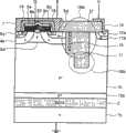
图1是表示实施方式1的IGBT的截面图。如图1所示,在实施方式1中使用SOI基板制作n沟道IGBT。SOI基板为在p支撑基板1a上依次层叠有由氧化膜等构成的绝缘层2、n+少数载流子抵消层13a和n-漂移区域3a的结构。FIG. 1 is a cross-sectional view showing an IGBT according to
n-漂移区域3a的电阻率比n+少数载流子抵消层13a的电阻率高。因此,n+少数载流子抵消层13a具有对金属离子污染的消除(gettering)效果,兼作消除层。n-漂移区域3a相当于第一半导体区域,n+少数载流子抵消层13a相当于在支撑基板上隔着绝缘层设置的半导体层。The resistivity of the n− drift region 3 a is higher than that of the n+ minority carrier offset
在n-漂移区域3a的表面层的一部分设置有n阱区3b。n阱区3b与n-漂移区域3a相比,更高浓度地掺杂,具有比n-漂移区域3a低的电阻率。因此,抑制由后述的与p基极区域4a的JFET(结型FET)效果引起的n阱区3b的电阻的增大。An n- well region 3b is provided in a part of the surface layer of the n-
p基极区域4a在n-漂移区域3a的表面层的一部分,与n-漂移区域3a和n阱区3b连接设置。n阱区3b和p基极区域4a分别相当于第二半导体区域和第三半导体区域。The p-
在p基极区域4a的一部分和n阱区3b的表面上,隔着栅极绝缘膜9a设置有栅极电极8a。栅极电极8a例如可以由导电性多晶硅构成。在图中,为了实现电容的降低在n阱区3b的表面上形成有厚的绝缘膜9c,其上设置有栅极电极8a。在p基极区域4a的另一部分,设置有p+电阻区域5a和p+基极接触区域5b。在p+低电阻区域5a的一部分设置有n+发射极区域6a。n+发射极区域6a以与栅极电极8a的p基极区域侧端部(在图1中,n+发射极区域6a上的端部)匹配的方式设置。栅极电极8a可以设置在n阱区3b与n+发射极区域6a之间的p基极区域4a的表面上,未必一定要设置在n阱区3b上。A
当栅极电压超过阈值电压时,在n+发射极区域6a与n阱区3b之间的p基极区域4a与栅极绝缘膜9a的界面上形成沟道。在p基极区域4a中,p+低电阻区域5a以占据n+发射极区域6a的下侧的方式形成,p+基极接触区域5b与n+发射极区域6a邻接设置。p+基极接触区域5b相当于高电导度区域。如本实施方式所示,优选p+低电阻区域5a以在n+发射极区域6a的下侧占据不影响阈值电压的范围的方式形成,但是也可以形成在n+发射极区域6a的下侧的一部分。When the gate voltage exceeds the threshold voltage, a channel is formed at the interface between
在栅极电极8a的p基极区域侧端部的外侧,设置有与该端部相接,由氧化膜或氮化膜构成的栅极侧壁隔板(spacer)区域18。利用该栅极侧壁隔板区域18,p+低电阻区域5a以不进入形成沟道的区域的方式形成。由此,p+低电阻区域5a不会对形成沟道的栅极电压的阈值造成影响。Outside the end of the
并且,在n-漂移区域3a的表面层的一部分,与n阱区3b和p基极区域4a分离设置有n缓冲区域11a。n缓冲区域11a与n-漂移区域3a相比,更高浓度地掺杂,具有比n-漂移区域3a低的电阻率。Furthermore, nbuffer region 11a is provided separately from
n缓冲区域11a相当于第四半导体区域,与n-漂移区域3a和n阱区3b一起成为保持设备的耐压的漂移区域。这样,本设备为具有n缓冲区域11a的穿通(punch through)型的IGBT。The
在n缓冲区域11a的一部分设置有p+集电极区域12a,通过n缓冲区域11a从n-漂移区域3a隔离。p+集电极区域12a为用于电导度调制的载流子注入区域。n缓冲区域11a控制从p+集电极区域12a注入的电导度调制载流子量,与元件导通电阻和关断损耗(turnoffloss)的权衡有关。A p+ collector region 12a is provided in a part of the
在n阱区3b以及p基极区域4a与n缓冲区域11a之间,上层沟槽16a从SOI基板表面形成至比p基极区域4a更深,到达n-漂移区域3a的位置。并且,从上层沟槽16a的底开始,比上层沟槽16a宽度窄的下层沟槽16b形成至更深的位置。Between the
这些上层沟槽16a和下层沟槽16b通过氧化膜等埋入沟槽绝缘膜17埋住。埋入沟槽绝缘膜17在上层沟槽16a的发射极侧侧壁中,与n-漂移区域3a、p基极区域4a以及p+基极接触区域5b相接。These upper-
在埋入沟槽绝缘膜17内的、上层沟槽16a的发射极侧侧壁的附近,由导电性多晶硅等构成的发射极侧场电极15以电漂移状态被埋入。发射极侧场电极15可以跨由p基极区域4a和n-漂移区域3a形成的PN结面的上下而设置。发射极侧场电极15相当于发射极侧导电区域。In the vicinity of the emitter-side sidewall of the
并且,埋入沟槽绝缘膜17,在上层沟槽16a的集电极侧侧壁中,与n-漂移区域3a和n缓冲区域11a相接。在埋入沟槽绝缘膜17内的、上层沟槽16a的集电极侧侧壁的附近,设置有由导电性多晶硅等构成的集电极侧场电极14。集电极侧场电极14相当于集电极侧导电区域,电连接于通过内部配线或者外部配线与p+集电极区域12a接触设置的集电极电极10,与集电极电极10为同电位。Further, the
集电极侧场电极14防止上层沟槽16a与n-漂移区域3a和n缓冲区域11a的界面的损耗,有助于设备的高耐压化。也就是说,通过设置集电极侧场电极14,能够实现设备的高耐压化。集电极侧场电极14可以跨与n-漂移区域3a和n缓冲区域11a的界面的上下而设置。The
与n+发射极区域6a和p+基极接触区域5b这两者接触,将p+基极接触区域5b和n+发射极区域6a短路设置有发射极电极7。在图1中,符号20表示在制造时,为了降低对栅极绝缘膜9a的等离子体蚀刻损害而设置的氧化膜等绝缘膜覆盖层,符号21表示层间绝缘膜。In contact with both the n+ emitter region 6 a and the p+
在以上的结构中,得到使电导度调制载流子迂回的迂回结构的栅极构造。即,从p+集电极区域12a注入的载流子的一部分,通过p基极区域4a与n-漂移区域3a的界面、p基极区域4a和p+基极接触区域5b,到达发射极电极7。In the above structure, the gate structure of the detour structure which detours the conductivity-modulated carriers is obtained. That is, part of the carriers injected from the p+ collector region 12a reaches the emitter electrode through the interface between the
从p+集电极区域12a注入的其他载流子,通过n阱区3b、p基极区域4a与栅极绝缘膜9a的界面的表面沟道、p+低电阻区域5a和p+基极接触区域5b,到达发射极电极7。通过这样的迂回结构,设备很难被闭锁,提高抗闭锁能力。Other carriers injected from the p+ collector region 12a pass through the
接着,参照图2~图8对图1所示结构的设备的制造程序进行说明。首先,如图2所示,在由作为n-漂移区域3a的n-半导体构成的晶片的表面形成屏蔽(screen)氧化膜31。从其上离子注入作为n型杂质的As(砷)并进行热扩散,如图3所示,在晶片表面形成n+少数载流子抵消层13a。并且,如图4所示,除去屏蔽氧化膜31。至此,完成设备晶片。Next, a manufacturing procedure of the device having the configuration shown in FIG. 1 will be described with reference to FIGS. 2 to 8 . First, as shown in FIG. 2 , a
另一方面,如图5所示,准备p支撑基板1a。然后如图6所示,在p支撑基板1a的表面形成氧化膜等绝缘层2,作为处理晶片。接着,如图7所示,使处理晶片的绝缘层2的表面与设备晶片的n+少数载流子抵消层13a的表面贴合。这时,设备晶片和处理晶片隔着设备晶片的表面的自然氧化膜被结合而一体化。然后,如图8所示,将一体化后的SOI晶片的n-漂移区域3a研磨至规定的厚度。至此,SOI晶片完成。On the other hand, as shown in FIG. 5, a p-supporting
关于以后的制造程序,没有特别图示,但是接下来通过磷等的离子注入,在SOI晶片的表面,即n-漂移区域3a的被研磨的表面形成作为n阱区3b和n缓冲区域11a的n扩散层。接下来,进行硼等的离子注入,并进行热扩散形成p基极区域4a。The subsequent manufacturing process is not particularly shown, but next, by ion implantation of phosphorus or the like, the n well region3b and the
接着,形成沟槽蚀刻用的硬掩膜,通过沟槽蚀刻形成下层沟槽16b。通过牺牲氧化等除去沟槽蚀刻的损害后,在晶片的整个面上堆积氧化膜等绝缘膜。Next, a hard mask for trench etching is formed, and the
通过CMP使堆积的绝缘膜表面平坦化之后,形成沟槽蚀刻用的硬掩膜,通过进行下层沟槽16b的两侧壁的上部的蚀刻形成上层沟槽16a。通过牺牲氧化等除去沟槽蚀刻的损害后,在上层沟槽16a的侧壁和底面堆积氧化膜等绝缘膜。接着,在上层沟槽16a堆积导电性多晶硅。After the surface of the deposited insulating film is flattened by CMP, a hard mask for trench etching is formed, and
对堆积的导电性多晶硅膜进行回蚀(etch back)之后,在晶片整个面上堆积氧化膜等绝缘膜并通过CMP进行平坦化。之后,留下沟槽16a和沟槽16b上的绝缘膜,使晶片表面露出。在露出的晶片表面上,将氮化膜作为掩膜使用,形成作为绝缘膜9c的LOCOS氧化膜。After etching back the deposited conductive polysilicon film, an insulating film such as an oxide film is deposited on the entire surface of the wafer and planarized by CMP. After that, the insulating film on the
接着,在其上成长作为栅极绝缘膜9a的氧化膜。在该栅极绝缘膜9a和绝缘膜9c上,堆积300~400nm厚度的作为栅极电极8a的掺杂多晶硅。Next, an oxide film as
进一步在其上,堆积300~500nm厚度的作为绝缘膜覆盖层20的氧化膜等。由于存在该绝缘膜覆盖层20,因此在本实施方式中,作为栅极电极8a的掺杂多晶硅的厚度能够薄至300~400nm,容易实现LV(低电压)CMOS设备与栅极多晶硅的共通化。Furthermore, an oxide film or the like as the insulating
接着,通过RIE(活性离子蚀刻),形成由绝缘膜覆盖层20、栅极电极8a和栅极绝缘膜9a构成的栅层叠(gate stack)结构。这时,通过设置作为绝缘膜覆盖层20的氧化膜等,降低对栅极绝缘膜9a的等离子体蚀刻损害。Next, by RIE (Reactive Ion Etching), a gate stack structure composed of the insulating
在进行遮蔽氧化(shadow oxidation)之后,通过自我对准(自我匹配技术)进行砷等的离子注入,形成n+发射极区域6a。接着,在栅层叠结构的侧面形成栅极侧壁隔板区域18。这时,需要使栅极侧壁隔板区域18的厚度为150~200nm左右。这是为了在接下来的硼的离子注入工序中,抵消硼离子的横向飞行距离,抑制对形成沟道的栅极电压的阈值带来影响。After performing shadow oxidation, ion implantation of arsenic or the like is performed by self-alignment (self-alignment technique) to form n+ emitter region 6a. Next, gate
之后,以例如70~90keV的高能量和1×10¹⁵~3×1015cm-2的剂量进行硼的离子注入,在n+发射极区域6a的下面形成p+低电阻区域5a。这时,通过绝缘膜覆盖层20和栅极电极8a阻止向沟道区域的硼离子的注入,保护沟道区域。Afterwards, boron ion implantation is performed at a high energy of, for example, 70-90keV and a dose of 1×10¹⁵ to 3×1015 cm−2 to form a p+ low-
接着,通过硼的离子注入形成p+基极接触区域5b和p+集电极区域12a。接着,在晶片整个面上堆积层间绝缘膜21,通过CMP(化学机械研磨)使上表面平坦化。然后,在平坦化后的层间绝缘膜21上开接触孔,溅射金属,形成发射极电极7和集电极电极10,完成前段工序。Next, p+
然而,关于上述SOI晶片的制作,有如下的报告。However, the following reports have been made regarding the production of the above-mentioned SOI wafer.
首先,是关于抑制OSF(氧化导入层叠缺陷)和BMD(体微缺陷:Bulk Micro Defect)的发生的报告。在基于提拉法(Czochralski method)的晶片引出过程中形成的原子空穴与晶格间原子的平衡,例如由于以高剂量注入硼离子而被破坏。因此,如果以900℃以下的温度进行离子注入后的最初的退火处理,会导致OSF和BMD大量发生。First, it is a report on suppressing the occurrence of OSF (Oxidation Introduced Stacking Defect) and BMD (Bulk Micro Defect). The balance of atomic holes and interlattice atoms formed during wafer extraction based on the Czochralski method is disrupted, for example, by implanting boron ions in high doses. Therefore, if the initial annealing treatment after ion implantation is performed at a temperature of 900° C. or lower, a large amount of OSF and BMD will occur.
作为其对策,ジオング一ミン·キム(Jeong-Min Kim)等在“ビヘイビユア オブサ一マリインデユ一ストデイフエクツインヘビリボロン一ド一プドシリコンクリスタルズ(Behaviorof Thermally Induced Defects in Heavily Boron-Doped SiliconCrystals)”(应用物理的日本杂志(Japanese Journal ofApplied Physics),2001年3月,第40卷,第1部,第3A号,p.1370-1374)中,报告有当以高温(1050℃)进行最初的退火处理时,能够抑制OSF和BMD的发生。As a countermeasure, Jeong-Min Kim et al. published in "ビヘイビユアOBサマリインデュストデイフエクツインヘビリボロン一ドプドシリコンクリスタルズ (Behavior of Thermally Induced Defects in Heavily Boron-Doped Silicon Crystals )" (Japanese Journal of Applied Physics, March 2001, Vol. 40,
此外,关于晶片彼此的结合,报告如下。In addition, the bonding between wafers is reported as follows.
当制作贴合SOI晶片时,贴合的晶片的表面为晶片彼此的结合所需的镜面品质的表面。作为硅晶片彼此的结合的机构,公知的是晶片彼此通过吸附在相互的表面的“Si-OH-”的H2O形成为一体。When producing a bonded SOI wafer, the surface of the bonded wafer has a mirror quality surface required for the bonding of the wafers. As a mechanism for bonding silicon wafers, it is known that the wafers are integrated by H2 O of "Si-OH-" adsorbed on the surfaces of each other.
关于此,ア一ル·ステングル(R.Stengl)等在“アモデルフオアザシリコンフエハボンデイングプロセス(A Modelfor the Silicon Wafer Bonding Process)”(应用物理的日本杂志(JapaneseJournal of Applied Physics),1989年10月,第28卷,第10号,p.1735-1741)中,报告有当加热到200℃以上时,水分子变成四聚体簇(tetramer cluster),当加热到700℃以上时,水簇蒸发,通过“Si-O-Si”晶片彼此结合。再者,还报告有在1100℃被加热时,SOI晶片的绝缘层(埋入氧化膜层)逆流,晶片彼此的结合强度更进一步提高。Regarding this, R. Stengl et al. "A Model for the Silicon Wafer Bonding Process" (Japanese Journal of Applied Physics), 1989 October,
此外,晶片彼此的结合,如果在该结合前的镜面品质的晶片表面上存在羟基(“-OH”)则能够实现。ヒロアキ·ヒミ(Hiroaki Himi)等在“シリコンウエハダイレクトボンデイングウイズアウトハイドロフイリツクネイデイブオキサイヅ(Silicon WaferDirect Bonding without Hydrophilic Native Oxides)”(应用物理的日本杂志(Japanese Journal ofApplied Physics),1994年1月,第33卷,第1部,第1A号,p.6-10)中,报告有关于将刚经过高浓度氟酸处理之后的设备晶片浸入脱离子水中,将附着在设备基板的表面的面密度高的“-F”置换为“-OH”后,使设备晶片与形成有绝缘层的处理晶片结合的方法。In addition, bonding of the wafers can be realized if hydroxyl groups ("-OH") exist on the surface of the mirror-quality wafers before the bonding.ヒロアキ・ヒミ (Hiroaki Himi) et al. in "Silicon ウエハエハダイレクトbonding ウイズアウトハイドロフイリツクネイデイブオキサイヅ (Silicon Wafer Direct Bonding without Hydrophilic Native Oxides)" (Japanese Journals of
在本实施方式中,当制作SOI晶片时,能够适用上述三个报告。In the present embodiment, the above three reports can be applied when fabricating an SOI wafer.
依据上述的实施方式1的结构,在确保200V等级的耐压的情况下,能够使图1所示结构的设备间距为12μm以下,将n-漂移区域3a的厚度抑制在20μm以下,所以图1所示结构的设备间距变为图49所示的现有设备的单元间距(25μm)的一半以下。此外,图1所示结构的单位单元设备的电流驱动能力通过设备结构和制造程序的优化,变为与现有的横型设备的电流驱动能力相同程度。因此,在图1所示结构的设备中,每单位面积的导通电阻为现有设备的导通电阻(500mΩ·mm2)的一半的250mΩ·mm2左右。According to the above-mentioned structureof Embodiment 1, in the case of ensuring a withstand voltage of 200V class, the device pitch of the structure shown in FIG. The device pitch of the shown structure becomes less than half of the cell pitch (25 μm) of the conventional device shown in FIG. 49 . In addition, the current driving capability of the unit cell device with the structure shown in FIG. 1 becomes equivalent to the current driving capability of the conventional horizontal device through optimization of the device structure and manufacturing process. Therefore, in the device having the structure shown in FIG. 1 , the on-resistance per unit area is about 250 mΩ·mm2 , which is half of the on-resistance (500 mΩ·mm2 ) of the conventional device.
作为一个例子,将在图1所示的结构中,使D1为0.5μm、D2为0.6μm、2D3为1.8μm、n-漂移区域3a的厚度为12μm或者16μm时的设备的断开耐压(击穿电压)与n-漂移区域3a的掺杂浓度的关系示于图9。此外,将在图1所示的结构中,使D1为0.5μm、D2为0.6μm、2D3为1.8μm、n-漂移区域3a的厚度为16μm、n-漂移区域3a的掺杂浓度为3×1014cm-3时的击穿时的静电电位分布示于图10。在图10中,X表示设备的横方向的尺寸,Y表示设备的纵方向的尺寸。As an example, in the structure shown in FIG. 1, when D1 is 0.5 μm, D2 is 0.6 μm, 2D3 is 1.8 μm, and the thickness of the n- drift region 3a is 12 μm or 16 μm, the disconnection withstand voltage of the device ( The relationship between the breakdown voltage) and the doping concentration of the n- drift region 3a is shown in FIG. 9 . In addition, in the structure shown in FIG. 1, D1 is 0.5 μm, D2 is 0.6 μm, 2D3 is 1.8 μm, the thickness of n- drift region 3a is 16 μm, and the doping concentration of n- drift region 3a is 3× The electrostatic potential distribution at the time of breakdown at 1014 cm-3 is shown in Fig. 10 . In FIG. 10 , X represents the dimension in the horizontal direction of the device, and Y represents the dimension in the vertical direction of the device.
图11是表示使图1所示结构的n沟道IGBT的极性反转后的p沟道IGBT。关于该p沟道IGBT,在上述实施方式1的说明中,将p支撑基板1a、n+少数载流子抵消层13a、n-漂移区域3a、n阱区3b和p基极区域4a分别替换为n支撑基板1b、p+少数载流子抵消层13b、p-漂移区域3c、p阱区3d和n基极区域4b。FIG. 11 shows a p-channel IGBT obtained by inverting the polarity of the n-channel IGBT having the structure shown in FIG. 1 . Regarding this p-channel IGBT, in the description of
此外,将p+低电阻区域5a、p+基极接触区域5b、n+发射极区域6a、n缓冲区域11a和p+集电极区域12a分别替换为n+低电阻区域5c、n+基极接触区域5d、p+发射极区域6b、p缓冲区域11b和n+集电极区域12b。此外,关于制造程序的注入离子种类,调换n型杂质和p型杂质。In addition, p+
实施方式2
图12和图13分别是表示实施方式2的n沟道IGBT和p沟道IGBT的截面图。如图12和图13所示,实施方式2的IGBT是在实施方式1的IGBT中,相对各个单一的漂移区域3a、3c具有多个(图示的例子中为2个)沟道,具有高电流能力的结构。12 and 13 are cross-sectional views showing an n-channel IGBT and a p-channel IGBT of
具体而言,在图12所示的n沟道IGBT的情况下,在埋入沟槽绝缘膜17的发射极侧,夹着n阱区3b设置有多个,例如两个p基极区域4a。在各p基极区域4a内,设置有p+低电阻区域5a、p+基极接触区域5b和n+发射极区域6a。并且,在各n+发射极区域6a和n阱区3b之间的p基极区域4a上,设置有由栅极绝缘膜9a和栅极电极8a构成的平面栅结构,在各p基极区域4a和与其相对的栅极绝缘膜9a的界面上形成沟道。Specifically, in the case of the n-channel IGBT shown in FIG. 12, a plurality of, for example, two p-
此外,相邻的n+发射极区域6a和p+基极接触区域5b通过发射极电极7相互电连接。其他的结构与实施方式1的IGBT的结构相同,因此省略说明。Furthermore, adjacent n+ emitter region 6 a and p+
在图13所示的p沟道IGBT的情况下,进行与实施方式1同样的极性的替换。In the case of the p-channel IGBT shown in FIG. 13 , the same polarity replacement as in
实施方式3Embodiment 3
图14和图15分别是表示实施方式3的n沟道IGBT和p沟道IGBT的截面图。如图14和图15所示,实施方式3的各IGBT在实施方式1的各IGBT中,从晶片表面至沟槽底设置有一定宽度的沟槽16c,代替上层沟槽16a和下层沟槽16b,其中埋入有埋入沟槽绝缘膜17。其他的结构与实施方式1的IGBT的结构相同,因此省略说明。14 and 15 are cross-sectional views showing an n-channel IGBT and a p-channel IGBT of Embodiment 3, respectively. As shown in FIG. 14 and FIG. 15 , in each IGBT of Embodiment 3, in each IGBT of
实施方式4Embodiment 4
图16和图17分别是表示实施方式4的n沟道IGBT和p沟道IGBT的截面图。如图16和图17所示,实施方式4的各IGBT是将实施方式2和实施方式3对应的极性的IGBT分别组合的IGBT。即,相对各个单一的漂移区域3a、3c具有多个(图示的例子中为两个)沟道,并且从晶片表面至沟槽底设置有一定宽度的沟槽16c,其中埋入有埋入沟槽绝缘膜17。其他的结构与实施方式2的IGBT的结构和实施方式3的IGBT的结构相同,因此省略说明。16 and 17 are cross-sectional views showing an n-channel IGBT and a p-channel IGBT of Embodiment 4, respectively. As shown in FIGS. 16 and 17 , each IGBT of the fourth embodiment is an IGBT obtained by combining IGBTs of polarities corresponding to the second and third embodiments. That is, each
实施方式5Embodiment 5
图18和图19分别是表示实施方式5的n沟道IGBT和p沟道IGBT的截面图。如图18和图19所示,实施方式5的各IGBT是具有沟槽栅结构以代替实施方式1的各IGBT的平面栅结构的IGBT,具有难以闭锁的优点。18 and 19 are cross-sectional views showing an n-channel IGBT and a p-channel IGBT of Embodiment 5, respectively. As shown in FIGS. 18 and 19 , each IGBT of Embodiment 5 has a trench gate structure instead of the planar gate structure of each IGBT of
具体而言,在图18所示的n沟道IGBT的情况下,从晶片表面开始贯通p基极区域4a并到达n-漂移区域3a的栅极沟槽19,与埋入沟槽绝缘膜17分离,并且与p基极区域4a相接而形成。在栅极沟槽19的内侧,隔着栅极绝缘膜9b埋入有栅极电极8b。在p基极区域4a的一部分,n+发射极区域6a与栅极沟槽19相接设置。Specifically, in the case of n-channelIGBT shown in FIG. separated, and formed in contact with the
此外,在p基极区域4a的一部分,p+低电阻区域5a与n+发射极区域6a邻接设置。发射极电极7与n+发射极区域6a和p+低电阻区域5a这两者接触,将p+低电阻区域5a和n+发射极区域6a短路。并且,在实施方式5的IGBT中,未设置与p基极区域4a相接的n阱区3b。其他的结构与实施方式1的IGBT的结构相同,因此省略说明。In addition, in a part of
在图19所示的p沟道IGBT的情况下,进行与实施方式1同样的极性的替换。In the case of the p-channel IGBT shown in FIG. 19 , the same polarity replacement as in
实施方式6Embodiment 6
图20和图21分别是表示实施方式6的n沟道IGBT和p沟道IGBT的截面图。如图20和图21所示,实施方式6的IGBT是在实施方式5的IGBT中,相对各个单一的漂移区域3a、3c具有多个(图示的例子中为3个)沟道,具有高电流能力的结构。其他的结构与实施方式5的IGBT的结构相同,因此省略说明。20 and 21 are cross-sectional views showing an n-channel IGBT and a p-channel IGBT of Embodiment 6, respectively. As shown in FIGS. 20 and 21 , the IGBT of the sixth embodiment has a plurality of (three in the illustrated example) channels for each
实施方式7
图22和图23分别是表示实施方式7的n沟道IGBT和p沟道IGBT的截面图。如图22和图23所示,实施方式7的各IGBT在实施方式5的IGBT中,从晶片表面至沟槽底设置有一定宽度的沟槽16c,代替上层沟槽16a和下层沟槽16b,其中埋入有埋入沟槽绝缘膜17。其他的结构与实施方式5的IGBT的结构相同,因此省略说明。22 and 23 are cross-sectional views showing an n-channel IGBT and a p-channel IGBT of
实施方式8Embodiment 8
图24和图25分别是表示实施方式8的n沟道IGBT和p沟道IGBT的截面图。如图24和图25所示,实施方式8的各IGBT是将实施方式6和实施方式7对应的极性的IGBT分别组合的IGBT。即,相对各个单一的漂移区域3a、3c具有多个(图示的例子中为3个)沟道,并且从晶片表面至沟槽底设置有一定宽度的沟槽16c,其中埋入有埋入沟槽绝缘膜17。其他的结构与实施方式6的IGBT的结构和实施方式7的IGBT的结构相同,因此省略说明。24 and 25 are cross-sectional views showing an n-channel IGBT and a p-channel IGBT of Embodiment 8, respectively. As shown in FIGS. 24 and 25 , each IGBT of the eighth embodiment is an IGBT obtained by combining IGBTs of polarities corresponding to the sixth and seventh embodiments. That is, a plurality of (three in the illustrated example) trenches are provided for each
实施方式9
图26和图27分别是表示实施方式9的n沟道IGBT和p沟道IGBT的截面图。如图26和图27所示,实施方式9的各IGBT是在实施方式1的各IGBT中,未设置集电极侧场电极14的IGBT。并且,在n沟道IGBT中,将上层沟槽16a和n缓冲区域11a分离,在上层沟槽16a与n缓冲区域11a之间夹着n-漂移区域3a,由此抑制由n缓冲区域11a和n-漂移区域3a的界面的损耗引起的对设备的耐压的影响。26 and 27 are cross-sectional views showing an n-channel IGBT and a p-channel IGBT of
同样地,在p沟道IGBT中,将上层沟槽16a和p缓冲区域11b分离,在这之间夹着p-漂移区域3c,由此抑制由p缓冲区域11b和p-漂移区域3c的界面的损耗引起的对设备的耐压的影响。因此,实施方式9的各IGBT的设备间距比实施方式1的各IGBT的设备间距稍长,但是比图49所示的现有的设备的单元间距短。Similarly, in the p-channel IGBT, the
此外,实施方式9的各IGBT的单位单元设备的电流驱动能力,通过设备结构和制造程序的优化,变为与现有的横型设备的电流驱动能力相同程度,因此实施方式9的各IGBT的每单位面积的导通电阻比现有的设备的导通电阻小,并且短路容量上升。其他的结构与实施方式1的IGBT的结构相同,因此省略说明。In addition, the current driving capability of the unit cell device of each IGBT in
实施方式10
图28和图29分别是表示实施方式10的n沟道IGBT和p沟道IGBT的截面图。如图28和图29所示,实施方式10的IGBT是在实施方式9的IGBT中,相对各个单一的漂移区域3a、3c具有多个(图示的例子中为两个)沟道,具有高电流能力的结构。其他的结构与实施方式9的IGBT的结构相同,因此省略说明。28 and 29 are cross-sectional views showing an n-channel IGBT and a p-channel IGBT of
实施方式11Embodiment 11
图30和图31分别是表示实施方式11的n沟道IGBT和p沟道IGBT的截面图。如图30和图31所示,实施方式11的各IGBT在实施方式9的各IGBT中,从晶片表面至沟槽底设置有一定宽度的沟槽16c,代替上层沟槽16a和下层沟槽16b,其中埋入有埋入沟槽绝缘膜17。其他的结构与实施方式9的IGBT的结构相同,因此省略说明。30 and 31 are cross-sectional views showing an n-channel IGBT and a p-channel IGBT of Embodiment 11, respectively. As shown in FIG. 30 and FIG. 31 , in each IGBT of Embodiment 11, in each IGBT of
实施方式12Embodiment 12
图32和图33分别是表示实施方式12的n沟道IGBT和p沟道IGBT的截面图。如图32和图33所示,实施方式12的各IGBT是将实施方式10和实施方式11对应的极性的IGBT分别组合的IGBT。即,相对各个单一的漂移区域3a、3c具有多个(图示的例子中为两个)沟道,并且从晶片表面至沟槽底设置有一定宽度的沟槽16c,其中埋入有埋入沟槽绝缘膜17。其他的结构与实施方式10的IGBT的结构和实施方式11的IGBT的结构相同,因此省略说明。32 and 33 are cross-sectional views showing an n-channel IGBT and a p-channel IGBT of Embodiment 12, respectively. As shown in FIGS. 32 and 33 , each IGBT of the twelfth embodiment is an IGBT obtained by combining IGBTs of polarities corresponding to the tenth embodiment and the eleventh embodiment. That is, each
实施方式13Embodiment 13
图34和图35分别是表示实施方式13的n沟道IGBT和p沟道IGBT的截面图。如图34和图35所示,实施方式13的各IGBT是在实施方式5的各IGBT中,未设置集电极侧场电极14的IGBT。并且,在n沟道IGBT中,将上层沟槽16a和n缓冲区域11a分离,在上层沟槽16a与n缓冲区域11a之间夹着n-漂移区域3a,由此抑制由n缓冲区域11a和n-漂移区域3a的界面的损耗引起的对设备的耐压的影响。34 and 35 are cross-sectional views showing an n-channel IGBT and a p-channel IGBT of Embodiment 13, respectively. As shown in FIGS. 34 and 35 , each IGBT of Embodiment 13 is an IGBT in which collector-
同样地,在p沟道IGBT中,将上层沟槽16a和p缓冲区域11b分离,在这之间夹着p-漂移区域3c,由此抑制由p缓冲区域11b和p-漂移区域3c的界面的损耗引起的对设备的耐压的影响。因此,实施方式13的各IGBT的设备间距比实施方式5的各IGBT的设备间距稍长,但是比图49所示的现有的设备的单元间距短。Similarly, in the p-channel IGBT, the
此外,实施方式13的各IGBT的单位单元设备的电流驱动能力,通过设备结构和制造程序的优化,变为与现有的横型设备的电流驱动能力相同程度,因此实施方式13的各IGBT的每单位面积的导通电阻比现有的设备的导通电阻小。其他的结构与实施方式5的IGBT的结构相同,因此省略说明。In addition, the current driving capability of the unit cell device of each IGBT in the thirteenth embodiment is equal to the current driving capability of the conventional horizontal device through optimization of the device structure and manufacturing process. Therefore, each IGBT in the thirteenth embodiment On-resistance per unit area is smaller than that of conventional devices. The rest of the structure is the same as that of the IGBT of Embodiment 5, and thus description thereof will be omitted.
实施方式14
图36和图37分别是表示实施方式14的n沟道IGBT和p沟道IGBT的截面图。如图36和图37所示,实施方式14的IGBT是在实施方式13的IGBT中,相对各个单一的漂移区域3a、3c具有多个(图示的例子中为3个)沟道,具有高电流能力的结构。其他的结构与实施方式13的IGBT的结构相同,因此省略说明。36 and 37 are cross-sectional views showing an n-channel IGBT and a p-channel IGBT of
实施方式15
图38和图39分别是表示实施方式15的n沟道IGBT和p沟道IGBT的截面图。如图38和图39所示,实施方式15的各IGBT在实施方式13的各IGBT中,从晶片表面至沟槽底设置有一定宽度的沟槽16c,代替上层沟槽16a和下层沟槽16b,其中埋入有埋入沟槽绝缘膜17。其他的结构与实施方式13的IGBT的结构相同,因此省略说明。38 and 39 are cross-sectional views showing an n-channel IGBT and a p-channel IGBT of
实施方式16Embodiment 16
图40和图41分别是表示实施方式16的n沟道IGBT和p沟道IGBT的截面图。如图40和图41所示,实施方式16的各IGBT是将实施方式14和实施方式15对应的极性的IGBT分别组合的IGBT。即,相对各个单一的漂移区域3a、3c具有多个(图示的例子中为3个)沟道,并且从晶片表面至沟槽底设置有一定宽度的沟槽16c,其中埋入有埋入沟槽绝缘膜17。其他的结构与实施方式14的IGBT的结构和实施方式15的IGBT的结构相同,因此省略说明。40 and 41 are cross-sectional views showing an n-channel IGBT and a p-channel IGBT of Embodiment 16, respectively. As shown in FIGS. 40 and 41 , each IGBT of Embodiment 16 is an IGBT obtained by combining IGBTs of polarities corresponding to Embodiments 14 and 15. That is, a plurality of (three in the illustrated example) trenches are provided for each
实施方式17
图42和图43分别是表示实施方式17的n沟道IGBT和p沟道IGBT的截面图。如图42和图43所示,实施方式17的n沟道IGBT是在实施方式1的n沟道IGBT中,使埋入沟槽绝缘膜17仅与n-漂移区域3a、n阱区3b和n缓冲区域11a接触的IGBT。即,埋入沟槽绝缘膜17不与p基极区域4a和p+基极接触区域5b接触。42 and 43 are cross-sectional views showing an n-channel IGBT and a p-channel IGBT of
因此,在实施方式17中,不需要发射极侧场电极15。从p+集电极区域12a注入的载流子,通过n阱区3b、p基极区域4a与栅极绝缘膜9a的界面的表面沟道、p+低电阻区域5a和p+基极接触区域5b到达发射极电极7。Therefore, in
同样地,在p沟道IGBT中,埋入沟槽绝缘膜17仅与p-漂移区域3c、p阱区3d和p缓冲区域11b接触,不与n基极区域4b和n+基极接触区域5d接触。因此,未设置发射极侧场电极15。从n+集电极区域12b注入的载流子,通过p阱区3d、n基极区域4b与栅极绝缘膜9a的界面的表面沟道、n+低电阻区域5c和n+基极接触区域5d到达发射极电极7。Likewise, in the p-channel IGBT, the buried
实施方式17的各IGBT的设备间距比图49所示的现有的设备的单元间距短。并且,实施方式17的各IGBT的单位单元设备的电流驱动能力,通过设备结构和制造程序的优化,变为与现有的横型设备的电流驱动能力相同程度,因此,实施方式17的各IGBT的每单位面积的导通电阻比现有的设备的导通电阻小。其他结构与实施方式1的IGBT的结构相同,因此省略说明。The device pitch of each IGBT in
实施方式18
图44和图45分别是表示实施方式18的n沟道IGBT和p沟道IGBT的截面图。如图44和图45所示,实施方式18的各IGBT在实施方式17的各IGBT中,从晶片表面至沟槽底设置有一定宽度的沟槽16c,代替上层沟槽16a和下层沟槽16b,其中埋入有埋入沟槽绝缘膜17。其他的结构与实施方式17的IGBT的结构相同,因此省略说明。44 and 45 are cross-sectional views showing an n-channel IGBT and a p-channel IGBT of
实施方式19
图46和图47分别是表示实施方式19的n沟道IGBT和p沟道IGBT的截面图。如图46和图47所示,实施方式19的n沟道IGBT在实施方式1的n沟道IGBT中,使埋入沟槽绝缘膜17仅与n-漂移区域3a和n阱区3b接触,不与p基极区域4a和p+基极接触区域5b接触。因此,不需要发射极侧场电极15。46 and 47 are cross-sectional views showing an n-channel IGBT and a p-channel IGBT of
此外,不设置集电极侧场电极14,将沟槽16c和n缓冲区域11a分离,在这之间夹着n-漂移区域3a,由此抑制由n缓冲区域11a和n-漂移区域3a的界面的损耗引起的对设备的耐压的影响。从p+集电极区域12a被注入的载流子,通过n阱区3b、p基极区域4a与栅极绝缘膜9a的界面的表面沟道、p+低电阻区域5a和p+基极接触区域5b到达发射极电极7。In addition, the collector-
同样地,在p沟道IGBT中,埋入沟槽绝缘膜17仅与p-漂移区域3c和p阱区3d接触,不与n基极区域4b和n+基极接触区域5d接触。因此,未设置发射极侧场电极15。Likewise, in the p-channel IGBT, buried
此外,不设置集电极侧场电极14,将沟槽16c和p缓冲区域11b分离,在这之间夹着p-漂移区域3c,由此抑制由p缓冲区域11b和p-漂移区域3c的界面的损耗引起的对设备的耐压的影响。从n+集电极区域12b被注入的载流子,通过p阱区3d、n基极区域4b与栅极绝缘膜9a的界面的表面沟道、n+低电阻区域5c和n+基极接触区域5d到达发射极电极7。In addition, the
实施方式19的各IGBT的设备间距比实施方式17或者实施方式18的各IGBT的设备间距稍长,但是比图49所示的现有的设备的单元间距短。此外,实施方式19的各IGBT的单位单元设备的电流驱动能力,通过设备结构和制造程序的优化,变为与现有的横型设备的电流驱动能力相同程度,因此实施方式19的各IGBT的每单位面积的导通电阻比现有的设备的导通电阻小。其他的结构与实施方式1的IGBT的结构相同,因此省略说明。The device pitch of each IGBT in
这里,对本实施方式19的设备与上述专利文献2中公开的设备的不同点进行说明。在实施方式19的设备中,由于n+少数载流子抵消层13a(p+少数载流子抵消层13b)与绝缘层2整个面接触,所以在通过实施方式1中说明过的贴合施工法制作SOI晶片的情况下不要求贴合精度。因此,能够容易地进行制造。与此相对,在上述专利文献2中公开的设备中,由于要求μm级别的贴合精度,所以如上所述在制造上不优选。Here, differences between the device of the nineteenth embodiment and the device disclosed in
此外,图48是表示实施方式19的设备的平面布局的一个例子的图。如图48所示,在实施方式19的设备中,埋入沟槽绝缘膜17在n+发射极区域6a(p+发射极区域6b)与p+集电极区域12a(n+集电极区域12b)之间配置在晶片整个面上,因此实效的漂移长度变长,晶片表面的单元间距缩短。与此相对,在上述专利文献2中公开的设备中,如上所述不能缩短单元间距。In addition, FIG. 48 is a diagram showing an example of a planar layout of a device according to
再者,在本实施方式19的设备中,与上述专利文献2中公开的设备相同,根据埋入沟槽绝缘膜17与n+少数载流子抵消层13a(p+少数载流子抵消层13b)的距离,限制从p+集电极区域12a(n+集电极区域12b)注入的少数载流子的量。另一方面,由于不妨碍在沟道中流通的多数载流子的传导,所以具有确保沟道侧的多数载流子的浓度较高,降低沟道电阻的效果。并且,通过设置n阱区3b(p阱区3d),抑制JFET效果,因此能够实现导通电阻的削减和单元间距的缩短。此外,通过设置p+低电阻区域5a(n+低电阻区域5c),进一步提高抗闭锁能力。In addition, in the device of the nineteenth embodiment, similar to the device disclosed in the above-mentioned
如上所述,依据实施方式1~19,通过形成沟槽,将保持耐压的部分相对晶片表面设置在垂直方向上。由此,漂移区域在晶片的深度方向弯折并引出到晶片表面,所以实效的漂移长度变长。因此,即使实效的漂移长度与现有为同等长度,元件所需表面积也骤减。因此,每单位面积的导通电阻降低。As described above, according to
此外,依据实施方式1~19,n+少数载流子抵消层13a(p+少数载流子抵消层13b)为对金属污染的消除层,所以能够得到对金属污染的消除效果。因此,栅极绝缘膜9a、9b的可靠性提高。In addition, according to
并且,依据实施方式1~19,n+少数载流子抵消层13a(p+少数载流子抵消层13b)抑制与n-漂移区域3a(p-漂移区域3c)的界面以及与绝缘层2的界面的缺陷的影响,并且抑制来自p支撑基板1a(n支撑基板1b)的损耗效果。因此,n-漂移区域3a(p-漂移区域3c)像块层那样动作。Furthermore, according to
此外,依据实施方式1~19,n+少数载流子抵消层13a(p+少数载流子抵消层13b)的掺杂浓度高,载流子的寿命短。因此,根据埋入沟槽绝缘膜17的底与绝缘膜2和n+少数载流子抵消层13a(p+少数载流子抵消层13b)之间的距离,控制从p+集电极区域12a(n+集电极区域12b)注入的载流子的寿命,保持元件的逆恢复时间与导通电阻的平衡。In addition, according to
此外,依据实施方式1~8、17和18,通过集电极侧场电极14和埋入沟槽绝缘膜17,遮蔽在埋入沟槽绝缘膜17的集电极侧产生的横电场,缓和在由n-漂移区域3a(p-漂移区域3c)和p基极区域4a(n基极区域4b)形成的PN结所发生的电场。因此,难以引起电破坏。此外,由于集电极侧场电极14与集电极电极10同电位,因此n缓冲区域11a(p缓冲区域11b),即与埋入沟槽绝缘膜17相接的集电极侧的漂移区域的界面难以发生损耗,能够达到维持电压的效果。In addition, according to
因此,依据各实施方式,能够得到具有与使用现有的SOI基板的横型半导体装置同等以上的耐压和电流驱动能力,并且比现有的横型半导体装置的抗闭锁能力高,而且每单位面积的导通电阻低的IGBT。此外,通过使用SOI基板,能够容易地与CMOS设备集成。Therefore, according to each embodiment, it is possible to obtain a withstand voltage and current drive capability equal to or higher than that of a conventional lateral semiconductor device using an SOI substrate, and a higher latch-up resistance than a conventional lateral semiconductor device, and the IGBT with low on-resistance. Furthermore, by using an SOI substrate, it is possible to easily integrate with a CMOS device.
在上文中,本发明并不局限于上述各实施方式,能够有各种变更。此外,关于本发明的维持耐压的结构,也能够适用于需要高耐压的横型LDMOS晶体管等,能够实现每单位面积的导通电阻的降低。As mentioned above, this invention is not limited to each said embodiment, Various changes are possible. In addition, the structure for maintaining a breakdown voltage of the present invention can also be applied to a horizontal LDMOS transistor or the like requiring a high breakdown voltage, and it is possible to reduce the on-resistance per unit area.
产业上的可利用性Industrial availability
如上所述,本发明的IGBT对要求高的抗闭锁能力的高耐压开关元件有用,特别适用于在平板显示器的驱动IC或车载IC等输出段中使用的高耐压开关元件。As described above, the IGBT of the present invention is useful for high withstand voltage switching elements requiring high latch-up resistance, and is particularly suitable for high withstand voltage switching elements used in output stages such as driver ICs for flat panel displays and automotive ICs.
Claims (20)
Translated fromChineseApplications Claiming Priority (1)
| Application Number | Priority Date | Filing Date | Title |
|---|---|---|---|
| PCT/JP2005/018798WO2007043170A1 (en) | 2005-10-12 | 2005-10-12 | Soi trench lateral igbt |
Publications (2)
| Publication Number | Publication Date |
|---|---|
| CN101288176Atrue CN101288176A (en) | 2008-10-15 |
| CN101288176B CN101288176B (en) | 2010-08-25 |
Family
ID=37942439
Family Applications (1)
| Application Number | Title | Priority Date | Filing Date |
|---|---|---|---|
| CN2005800518236AExpired - Fee RelatedCN101288176B (en) | 2005-10-12 | 2005-10-12 | Traverse type IGBT of SOI groove |
Country Status (4)
| Country | Link |
|---|---|
| US (1) | US7910962B2 (en) |
| CN (1) | CN101288176B (en) |
| DE (1) | DE112005003720T5 (en) |
| WO (1) | WO2007043170A1 (en) |
Cited By (6)
| Publication number | Priority date | Publication date | Assignee | Title |
|---|---|---|---|---|
| CN102064192A (en)* | 2010-12-03 | 2011-05-18 | 电子科技大学 | SOI (Silicon On Insulator) lateral isolative gate bipolar transistor device |
| CN101694850B (en)* | 2009-10-16 | 2011-09-14 | 电子科技大学 | Carrier-storing grooved gate IGBT with P-type floating layer |
| CN102299152A (en)* | 2010-06-22 | 2011-12-28 | 茂达电子股份有限公司 | Double-conduction semiconductor assembly and manufacturing method thereof |
| CN104282740A (en)* | 2009-11-09 | 2015-01-14 | 苏州博创集成电路设计有限公司 | Silicon-on-insulator lateral P-type insulated gate bipolar transistor |
| CN104681433A (en)* | 2015-01-26 | 2015-06-03 | 电子科技大学 | Preparation method of FS-IGBT (Field Stop-Insulated Gate Bipolar Translator) |
| CN108987398A (en)* | 2018-09-11 | 2018-12-11 | 长鑫存储技术有限公司 | Semiconductor device and manufacturing method thereof |
Families Citing this family (15)
| Publication number | Priority date | Publication date | Assignee | Title |
|---|---|---|---|---|
| JP2008305998A (en)* | 2007-06-07 | 2008-12-18 | Fuji Electric Device Technology Co Ltd | Semiconductor device |
| JP5636848B2 (en)* | 2010-05-26 | 2014-12-10 | 株式会社デンソー | Horizontal insulated gate bipolar transistor |
| JP5246302B2 (en)* | 2010-09-08 | 2013-07-24 | 株式会社デンソー | Semiconductor device |
| CN103066116B (en)* | 2011-10-24 | 2015-12-02 | 上海华虹宏力半导体制造有限公司 | Bipolar transistor and manufacture method |
| JP5742672B2 (en)* | 2011-11-02 | 2015-07-01 | 株式会社デンソー | Semiconductor device |
| CN102969243B (en)* | 2012-12-07 | 2015-04-22 | 株洲南车时代电气股份有限公司 | Plane gate type IGBT (Insulated Gate Bipolar Translator) chip production method |
| US8809156B1 (en) | 2013-01-25 | 2014-08-19 | International Business Machines Corporation | Method for implementing deep trench enabled high current capable bipolar transistor for current switching and output driver applications |
| JP2014212252A (en)* | 2013-04-19 | 2014-11-13 | 株式会社東芝 | Semiconductor device |
| CN104518014A (en)* | 2013-09-27 | 2015-04-15 | 立锜科技股份有限公司 | Insulated gate bipolar transistor and its manufacturing method |
| US9406793B2 (en) | 2014-07-03 | 2016-08-02 | Broadcom Corporation | Semiconductor device with a vertical channel formed through a plurality of semiconductor layers |
| EP3439026B1 (en)* | 2016-03-31 | 2023-03-08 | Tohoku University | Semiconductor device |
| CN107527811B (en)* | 2016-06-21 | 2020-07-10 | 无锡华润上华科技有限公司 | Lateral insulated gate bipolar transistor and manufacturing method thereof |
| US10056481B2 (en)* | 2017-01-13 | 2018-08-21 | Globalfoundries Inc. | Semiconductor device structure |
| CN112909081B (en)* | 2021-02-09 | 2022-05-17 | 电子科技大学 | A lateral power device |
| CN115621124A (en)* | 2022-09-29 | 2023-01-17 | 上海积塔半导体有限公司 | Preparation method of insulated gate bipolar transistor |
Family Cites Families (12)
| Publication number | Priority date | Publication date | Assignee | Title |
|---|---|---|---|---|
| JPH02180074A (en)* | 1988-12-29 | 1990-07-12 | Fujitsu Ltd | Offset type field effect transistor and insulation gate type bipolar transistor |
| JPH0888357A (en) | 1994-09-16 | 1996-04-02 | Toshiba Corp | Lateral IGBT |
| EP0702411B1 (en)* | 1994-09-16 | 2002-11-27 | Kabushiki Kaisha Toshiba | High breakdown voltage semiconductor device with a buried MOS-gate structure |
| JPH0897411A (en) | 1994-09-21 | 1996-04-12 | Fuji Electric Co Ltd | Lateral high breakdown voltage trench MOSFET and manufacturing method thereof |
| JPH08139319A (en)* | 1994-11-11 | 1996-05-31 | Mitsubishi Electric Corp | Semiconductor device and manufacturing method thereof |
| US6194290B1 (en)* | 1998-03-09 | 2001-02-27 | Intersil Corporation | Methods for making semiconductor devices by low temperature direct bonding |
| JP2002083877A (en) | 2000-09-07 | 2002-03-22 | Sanyo Electric Co Ltd | Semiconductor integrated circuit device and method of manufacturing the same |
| JP3963071B2 (en) | 2000-09-12 | 2007-08-22 | 日産自動車株式会社 | Semiconductor device |
| JP4750933B2 (en)* | 2000-09-28 | 2011-08-17 | 株式会社東芝 | Thin punch-through power device |
| WO2003103036A1 (en)* | 2002-05-31 | 2003-12-11 | Koninklijke Philips Electronics N.V. | Trench-gate semiconductor device and method of manufacturing |
| JP4193662B2 (en)* | 2003-09-30 | 2008-12-10 | 富士電機デバイステクノロジー株式会社 | Trench lateral conductivity modulation semiconductor device and manufacturing method of semiconductor device |
| JP4725040B2 (en) | 2004-06-17 | 2011-07-13 | 富士電機システムズ株式会社 | SOI trench lateral IGBT |
- 2005
- 2005-10-12CNCN2005800518236Apatent/CN101288176B/ennot_activeExpired - Fee Related
- 2005-10-12WOPCT/JP2005/018798patent/WO2007043170A1/enactiveApplication Filing
- 2005-10-12DEDE112005003720Tpatent/DE112005003720T5/ennot_activeWithdrawn
- 2008
- 2008-04-13USUS12/102,000patent/US7910962B2/ennot_activeExpired - Fee Related
Cited By (11)
| Publication number | Priority date | Publication date | Assignee | Title |
|---|---|---|---|---|
| CN101694850B (en)* | 2009-10-16 | 2011-09-14 | 电子科技大学 | Carrier-storing grooved gate IGBT with P-type floating layer |
| CN104282740A (en)* | 2009-11-09 | 2015-01-14 | 苏州博创集成电路设计有限公司 | Silicon-on-insulator lateral P-type insulated gate bipolar transistor |
| CN104282740B (en)* | 2009-11-09 | 2017-03-01 | 苏州博创集成电路设计有限公司 | The transverse P-type igbt of silicon-on-insulator |
| CN102299152A (en)* | 2010-06-22 | 2011-12-28 | 茂达电子股份有限公司 | Double-conduction semiconductor assembly and manufacturing method thereof |
| CN102299152B (en)* | 2010-06-22 | 2013-07-17 | 茂达电子股份有限公司 | Double-conduction semiconductor assembly and manufacturing method thereof |
| CN102064192A (en)* | 2010-12-03 | 2011-05-18 | 电子科技大学 | SOI (Silicon On Insulator) lateral isolative gate bipolar transistor device |
| CN102064192B (en)* | 2010-12-03 | 2012-08-29 | 电子科技大学 | SOI (Silicon On Insulator) lateral isolative gate bipolar transistor device |
| CN104681433A (en)* | 2015-01-26 | 2015-06-03 | 电子科技大学 | Preparation method of FS-IGBT (Field Stop-Insulated Gate Bipolar Translator) |
| CN104681433B (en)* | 2015-01-26 | 2017-07-11 | 电子科技大学 | A kind of FS IGBT preparation method |
| CN108987398A (en)* | 2018-09-11 | 2018-12-11 | 长鑫存储技术有限公司 | Semiconductor device and manufacturing method thereof |
| CN108987398B (en)* | 2018-09-11 | 2023-09-12 | 长鑫存储技术有限公司 | Semiconductor device and preparation method thereof |
Also Published As
| Publication number | Publication date |
|---|---|
| WO2007043170A1 (en) | 2007-04-19 |
| US7910962B2 (en) | 2011-03-22 |
| DE112005003720T5 (en) | 2008-09-11 |
| US20090008675A1 (en) | 2009-01-08 |
| CN101288176B (en) | 2010-08-25 |
| WO2007043170A9 (en) | 2007-05-31 |
Similar Documents
| Publication | Publication Date | Title |
|---|---|---|
| US7910962B2 (en) | SOI trench lateral IGBT | |
| US9748229B2 (en) | Semiconductor device | |
| US9153666B1 (en) | LDMOS with corrugated drift region | |
| JP5515248B2 (en) | Semiconductor device | |
| US8940606B2 (en) | Method for fabricating trench type power transistor device | |
| EP3331025B1 (en) | Semiconductor device, rc-igbt, and method of manufacturing semiconductor device | |
| CN1260804C (en) | Semiconductor crystal plate and its manufacturing method and semiconductor device and its manufacturing method | |
| US11728421B2 (en) | Split trench gate super junction power device | |
| CN109659351B (en) | Insulated gate bipolar transistor | |
| JP2018067744A (en) | Semiconductor device and manufacturing method of semiconductor device | |
| CN103681862B (en) | Semiconductor devices and its manufacture method | |
| JP2012054378A (en) | Semiconductor device | |
| US7326969B1 (en) | Semiconductor device incorporating thyristor-based memory and strained silicon | |
| KR20080026182A (en) | High performance capacitors in planar back gates cmos | |
| CN103548132B (en) | Manufacturing method of semiconductor device | |
| WO2022004084A1 (en) | Semiconductor device | |
| CN102163623B (en) | The manufacture method of semiconductor element and semiconductor element | |
| JP4725040B2 (en) | SOI trench lateral IGBT | |
| CN108933176A (en) | Semiconductor devices and its manufacturing method | |
| JP5087816B2 (en) | Semiconductor device and manufacturing method thereof | |
| JP4232645B2 (en) | Trench lateral semiconductor device and manufacturing method thereof | |
| JP3354127B2 (en) | High voltage element and method of manufacturing the same | |
| CN107833915A (en) | Semiconductor devices | |
| JP2014192361A (en) | Semiconductor device and manufacturing method of the same | |
| CN102449770B (en) | 3D channel architecture for semiconductor devices |
Legal Events
| Date | Code | Title | Description |
|---|---|---|---|
| C06 | Publication | ||
| PB01 | Publication | ||
| C10 | Entry into substantive examination | ||
| SE01 | Entry into force of request for substantive examination | ||
| ASS | Succession or assignment of patent right | Owner name:FUJI MOTOR ELECTRONICS TECHNOLOGY CO., LTD. Free format text:FORMER OWNER: FUJI MOTOR STOCK CO., LTD. Effective date:20100510 Owner name:FUJI MOTOR SYSTEM CO., LTD. Free format text:FORMER OWNER: FUJI MOTOR ELECTRONICS TECHNOLOGY CO., LTD. Effective date:20100510 | |
| C41 | Transfer of patent application or patent right or utility model | ||
| COR | Change of bibliographic data | Free format text:CORRECT: ADDRESS; FROM: KANAGAWA PREFECTURE, JAPAN TO: TOKYO, JAPAN | |
| TA01 | Transfer of patent application right | Effective date of registration:20100510 Address after:Tokyo, Japan Applicant after:Fuji Electric Systems Co.,Ltd. Address before:Tokyo, Japan Applicant before:Fuji Electric Device Technology Co.,Ltd. Effective date of registration:20100510 Address after:Tokyo, Japan Applicant after:Fuji Electric Device Technology Co.,Ltd. Address before:Kanagawa Applicant before:Fuji Electric Holdings Co.,Ltd. | |
| C14 | Grant of patent or utility model | ||
| GR01 | Patent grant | ||
| ASS | Succession or assignment of patent right | Owner name:FUJI ELECTRIC CO., LTD. Free format text:FORMER OWNER: FUJI ELECTRIC SYSTEMS CO., LTD. Effective date:20111009 | |
| C41 | Transfer of patent application or patent right or utility model | ||
| TR01 | Transfer of patent right | Effective date of registration:20111009 Address after:Japan's Kawasaki City Patentee after:FUJI ELECTRIC Co.,Ltd. Address before:Tokyo, Japan Patentee before:Fuji Electric Systems Co.,Ltd. | |
| CF01 | Termination of patent right due to non-payment of annual fee | Granted publication date:20100825 Termination date:20161012 | |
| CF01 | Termination of patent right due to non-payment of annual fee |