CN101286298B - Pixel, organic light emitting display using the same, and associated methods - Google Patents
Pixel, organic light emitting display using the same, and associated methodsDownload PDFInfo
- Publication number
- CN101286298B CN101286298BCN2008100916135ACN200810091613ACN101286298BCN 101286298 BCN101286298 BCN 101286298BCN 2008100916135 ACN2008100916135 ACN 2008100916135ACN 200810091613 ACN200810091613 ACN 200810091613ACN 101286298 BCN101286298 BCN 101286298B
- Authority
- CN
- China
- Prior art keywords
- transistor
- node
- light emitting
- voltage
- organic light
- Prior art date
- Legal status (The legal status is an assumption and is not a legal conclusion. Google has not performed a legal analysis and makes no representation as to the accuracy of the status listed.)
- Active
Links
Images


Classifications
- G—PHYSICS
- G09—EDUCATION; CRYPTOGRAPHY; DISPLAY; ADVERTISING; SEALS
- G09G—ARRANGEMENTS OR CIRCUITS FOR CONTROL OF INDICATING DEVICES USING STATIC MEANS TO PRESENT VARIABLE INFORMATION
- G09G3/00—Control arrangements or circuits, of interest only in connection with visual indicators other than cathode-ray tubes
- G09G3/20—Control arrangements or circuits, of interest only in connection with visual indicators other than cathode-ray tubes for presentation of an assembly of a number of characters, e.g. a page, by composing the assembly by combination of individual elements arranged in a matrix no fixed position being assigned to or needed to be assigned to the individual characters or partial characters
- G09G3/22—Control arrangements or circuits, of interest only in connection with visual indicators other than cathode-ray tubes for presentation of an assembly of a number of characters, e.g. a page, by composing the assembly by combination of individual elements arranged in a matrix no fixed position being assigned to or needed to be assigned to the individual characters or partial characters using controlled light sources
- G09G3/30—Control arrangements or circuits, of interest only in connection with visual indicators other than cathode-ray tubes for presentation of an assembly of a number of characters, e.g. a page, by composing the assembly by combination of individual elements arranged in a matrix no fixed position being assigned to or needed to be assigned to the individual characters or partial characters using controlled light sources using electroluminescent panels
- G09G3/32—Control arrangements or circuits, of interest only in connection with visual indicators other than cathode-ray tubes for presentation of an assembly of a number of characters, e.g. a page, by composing the assembly by combination of individual elements arranged in a matrix no fixed position being assigned to or needed to be assigned to the individual characters or partial characters using controlled light sources using electroluminescent panels semiconductive, e.g. using light-emitting diodes [LED]
- G09G3/3208—Control arrangements or circuits, of interest only in connection with visual indicators other than cathode-ray tubes for presentation of an assembly of a number of characters, e.g. a page, by composing the assembly by combination of individual elements arranged in a matrix no fixed position being assigned to or needed to be assigned to the individual characters or partial characters using controlled light sources using electroluminescent panels semiconductive, e.g. using light-emitting diodes [LED] organic, e.g. using organic light-emitting diodes [OLED]
- G09G3/3225—Control arrangements or circuits, of interest only in connection with visual indicators other than cathode-ray tubes for presentation of an assembly of a number of characters, e.g. a page, by composing the assembly by combination of individual elements arranged in a matrix no fixed position being assigned to or needed to be assigned to the individual characters or partial characters using controlled light sources using electroluminescent panels semiconductive, e.g. using light-emitting diodes [LED] organic, e.g. using organic light-emitting diodes [OLED] using an active matrix
- G09G3/3233—Control arrangements or circuits, of interest only in connection with visual indicators other than cathode-ray tubes for presentation of an assembly of a number of characters, e.g. a page, by composing the assembly by combination of individual elements arranged in a matrix no fixed position being assigned to or needed to be assigned to the individual characters or partial characters using controlled light sources using electroluminescent panels semiconductive, e.g. using light-emitting diodes [LED] organic, e.g. using organic light-emitting diodes [OLED] using an active matrix with pixel circuitry controlling the current through the light-emitting element
- G—PHYSICS
- G09—EDUCATION; CRYPTOGRAPHY; DISPLAY; ADVERTISING; SEALS
- G09G—ARRANGEMENTS OR CIRCUITS FOR CONTROL OF INDICATING DEVICES USING STATIC MEANS TO PRESENT VARIABLE INFORMATION
- G09G3/00—Control arrangements or circuits, of interest only in connection with visual indicators other than cathode-ray tubes
- G09G3/20—Control arrangements or circuits, of interest only in connection with visual indicators other than cathode-ray tubes for presentation of an assembly of a number of characters, e.g. a page, by composing the assembly by combination of individual elements arranged in a matrix no fixed position being assigned to or needed to be assigned to the individual characters or partial characters
- G09G3/22—Control arrangements or circuits, of interest only in connection with visual indicators other than cathode-ray tubes for presentation of an assembly of a number of characters, e.g. a page, by composing the assembly by combination of individual elements arranged in a matrix no fixed position being assigned to or needed to be assigned to the individual characters or partial characters using controlled light sources
- G09G3/30—Control arrangements or circuits, of interest only in connection with visual indicators other than cathode-ray tubes for presentation of an assembly of a number of characters, e.g. a page, by composing the assembly by combination of individual elements arranged in a matrix no fixed position being assigned to or needed to be assigned to the individual characters or partial characters using controlled light sources using electroluminescent panels
- G09G3/32—Control arrangements or circuits, of interest only in connection with visual indicators other than cathode-ray tubes for presentation of an assembly of a number of characters, e.g. a page, by composing the assembly by combination of individual elements arranged in a matrix no fixed position being assigned to or needed to be assigned to the individual characters or partial characters using controlled light sources using electroluminescent panels semiconductive, e.g. using light-emitting diodes [LED]
- H—ELECTRICITY
- H05—ELECTRIC TECHNIQUES NOT OTHERWISE PROVIDED FOR
- H05B—ELECTRIC HEATING; ELECTRIC LIGHT SOURCES NOT OTHERWISE PROVIDED FOR; CIRCUIT ARRANGEMENTS FOR ELECTRIC LIGHT SOURCES, IN GENERAL
- H05B33/00—Electroluminescent light sources
- H05B33/12—Light sources with substantially two-dimensional radiating surfaces
- G—PHYSICS
- G09—EDUCATION; CRYPTOGRAPHY; DISPLAY; ADVERTISING; SEALS
- G09G—ARRANGEMENTS OR CIRCUITS FOR CONTROL OF INDICATING DEVICES USING STATIC MEANS TO PRESENT VARIABLE INFORMATION
- G09G2300/00—Aspects of the constitution of display devices
- G09G2300/08—Active matrix structure, i.e. with use of active elements, inclusive of non-linear two terminal elements, in the pixels together with light emitting or modulating elements
- G09G2300/0809—Several active elements per pixel in active matrix panels
- G09G2300/0819—Several active elements per pixel in active matrix panels used for counteracting undesired variations, e.g. feedback or autozeroing
- G—PHYSICS
- G09—EDUCATION; CRYPTOGRAPHY; DISPLAY; ADVERTISING; SEALS
- G09G—ARRANGEMENTS OR CIRCUITS FOR CONTROL OF INDICATING DEVICES USING STATIC MEANS TO PRESENT VARIABLE INFORMATION
- G09G2300/00—Aspects of the constitution of display devices
- G09G2300/08—Active matrix structure, i.e. with use of active elements, inclusive of non-linear two terminal elements, in the pixels together with light emitting or modulating elements
- G09G2300/0809—Several active elements per pixel in active matrix panels
- G09G2300/0842—Several active elements per pixel in active matrix panels forming a memory circuit, e.g. a dynamic memory with one capacitor
- G09G2300/0852—Several active elements per pixel in active matrix panels forming a memory circuit, e.g. a dynamic memory with one capacitor being a dynamic memory with more than one capacitor
- G—PHYSICS
- G09—EDUCATION; CRYPTOGRAPHY; DISPLAY; ADVERTISING; SEALS
- G09G—ARRANGEMENTS OR CIRCUITS FOR CONTROL OF INDICATING DEVICES USING STATIC MEANS TO PRESENT VARIABLE INFORMATION
- G09G2320/00—Control of display operating conditions
- G09G2320/04—Maintaining the quality of display appearance
- G09G2320/043—Preventing or counteracting the effects of ageing
- G09G2320/045—Compensation of drifts in the characteristics of light emitting or modulating elements
Landscapes
- Engineering & Computer Science (AREA)
- Physics & Mathematics (AREA)
- Computer Hardware Design (AREA)
- General Physics & Mathematics (AREA)
- Theoretical Computer Science (AREA)
- Electroluminescent Light Sources (AREA)
- Control Of El Displays (AREA)
- Control Of Indicators Other Than Cathode Ray Tubes (AREA)
Abstract
Description
Technical field
Embodiment relates to a kind of pixel of the deterioration of Organic Light Emitting Diode, a kind of organic light-emitting display device and driving method thereof that utilizes this pixel of compensating automatically therein.
Background technology
Manufacturing and operation, very the operation unanimity of the pixel element of desired display device at display (for example, being used for reproducing the display of text, image, video etc.).Yet, can be difficult to provide this uniform operation.For example, in some display techniques, for example, in the display technique of utilization as the electroluminescent cell of Organic Light Emitting Diode (OLED), the operating characteristic of pixel element (for example, brightness) can change along with the time.Therefore, the display that needs a kind of change of the operating characteristic that be suitable for the compensation pixel element.
Summary of the invention
Therefore, target of the present invention provides and a kind ofly can compensate the pixel of the deterioration of Organic Light Emitting Diode, a kind of organic light-emitting display device and driving method thereof.
In order to finish above-mentioned target, a kind of pixel according to an embodiment of the invention is provided, this pixel comprises: Organic Light Emitting Diode; Transistor seconds is used for electric current is provided to Organic Light Emitting Diode; Image element circuit is used to compensate the threshold voltage of transistor seconds; Compensating unit is used to control the voltage of the gate electrode of transistor seconds, and with the deterioration of compensation Organic Light Emitting Diode, wherein, compensating unit comprises: the 7th transistor and the 8th transistor are combined between the Organic Light Emitting Diode and first power supply; First feedback condenser and second feedback condenser, between Section Point and first node, described Section Point is the 7th transistor and the 8th transistorized common node, the first node electricity is attached to the gate electrode of transistor seconds; The 9th transistor is combined between the 3rd node and the predetermined voltage source, and described the 3rd node is the common node of first feedback condenser and second feedback condenser.
Preferably, image element circuit comprises: the first transistor, be attached to i (i is a natural number) sweep trace and data line, and conducting is provided to first electrode of transistor seconds with the data-signal that will be provided to described data line when sweep signal is provided to the i sweep trace; The 3rd transistor is combined between second electrode and first node of transistor seconds, and conducting when sweep signal is provided to the i sweep trace; The 4th transistor is combined between initialize power and the first node, and conducting when sweep signal is provided to the i-1 sweep trace; The 5th transistor is combined between first electrode and first power supply of transistor seconds, and conducting when not providing led control signal to i light emitting control line; The 6th transistor is combined between second electrode and Organic Light Emitting Diode of transistor seconds, and conducting when not providing led control signal to i light emitting control line; Holding capacitor is combined between the first node and first power supply.Initialize power is configured to the magnitude of voltage less than data-signal.The 7th transistor and the 8th transistor are by conducting alternately and end.
A kind of organic light-emitting display device according to the embodiment of the invention is provided, and this organic light-emitting display device comprises: scanner driver is used for sweep signal sequentially is provided to sweep trace, and led control signal sequentially is provided to the light emitting control line; Data driver is used for data-signal is provided to data line; Pixel is positioned at the zone of being divided by sweep trace and data line, and wherein, each in the pixel comprises: Organic Light Emitting Diode; Transistor seconds is used for electric current is provided to Organic Light Emitting Diode; Image element circuit is used to compensate the threshold voltage of transistor seconds; Compensating unit is used to control the voltage of the gate electrode of transistor seconds, and with the deterioration of compensation Organic Light Emitting Diode, wherein, compensating unit comprises: the 7th transistor and the 8th transistor are combined between the Organic Light Emitting Diode and first power supply; First feedback condenser and second feedback condenser, between Section Point and first node, described Section Point is the 7th transistor and the 8th transistorized common node, the first node electricity is attached to the gate electrode of transistor seconds; The 9th transistor is combined between the 3rd node and the predetermined voltage source, and described the 3rd node is the common node of first feedback condenser and second feedback condenser.
Preferably, scanner driver is provided to i light emitting control line with led control signal, with overlapping with the sweep signal that is provided to i-1 (i is a natural number) sweep trace and i sweep trace.Image element circuit comprises: the first transistor be attached to i (i is a natural number) sweep trace and data line, and conducting is provided to first electrode of transistor seconds with the data-signal that will be provided to described data line when sweep signal is provided to the i sweep trace; The 3rd transistor is combined between second electrode and first node of transistor seconds, and conducting when sweep signal is provided to the i sweep trace; The 4th transistor is combined between initialize power and the first node, and conducting when sweep signal is provided to the i-1 sweep trace; The 5th transistor is combined between first electrode and first power supply of transistor seconds, and conducting when not providing led control signal to i light emitting control line; The 6th transistor is combined between second electrode and Organic Light Emitting Diode of transistor seconds, and conducting when not providing led control signal to i light emitting control line; Holding capacitor is combined between the first node and first power supply.Initialize power is configured to the magnitude of voltage less than data-signal.The 7th transistor and the 8th transistor are by conducting alternately and end.
A kind of driving method of the organic light-emitting display device according to the embodiment of the invention is provided, and described organic light-emitting display device comprises: the first transistor and transistor seconds, between the anode and first power supply of Organic Light Emitting Diode; First feedback condenser and second feedback condenser, between the gate electrode of first node and driving transistors, first node is the common node of the first transistor and transistor seconds, and the step that described driving method comprises is as follows: utilize the voltage of initialize power to make the voltage initialization of the gate electrode of driving transistors; Connect driving transistors by form, in holding capacitor, charge into threshold voltage and the corresponding voltage of data-signal with driving transistors with diode; The electric current corresponding with charging into voltage in holding capacitor is provided to Organic Light Emitting Diode; The voltage that is applied to Organic Light Emitting Diode is applied to first node; Be provided in the step process of first node in the step that voltage is filled into holding capacitor and the voltage that will be applied to Organic Light Emitting Diode, make Section Point maintain constant voltage, Section Point is the common port of first feedback condenser and second feedback condenser; Be set to floating state by Section Point, make the voltage of first node rise to first power source voltage simultaneously, come the voltage of the transistorized gate electrode of controlling and driving.
Description of drawings
Describe exemplary embodiment of the present invention in detail by the reference accompanying drawing, above-mentioned and further feature and advantage will become clearer for the ordinary skill in the art, wherein:
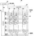
Fig. 1 shows the synoptic diagram according to the organic light emitting display of first embodiment;
Fig. 2 shows the synoptic diagram according to the pixel of first embodiment;
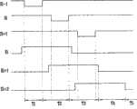
Fig. 3 shows the waveform that is used to drive the pixel shown in Fig. 2;
Fig. 4 shows the synoptic diagram according to the pixel of second embodiment;
Fig. 5 shows the waveform that is used to drive the pixel shown in Fig. 4.
Embodiment
Now, example embodiment is described with reference to the accompanying drawings hereinafter more fully; Yet these example embodiment can be implemented with different forms, should not be understood that to be limited to the embodiment in this proposition.On the contrary, it will be completely with complete in order to make the disclosure that these embodiment are provided, and will convey to those skilled in the art to scope of the present invention fully.
In the accompanying drawings, clear for what illustrate, can exaggerate the layer and the zone size, maybe can omit element.Should also be understood that when layer or element be known as " " another layer or another substrate " on " time, this layer or element can be directly in another layer or another substrate, perhaps also can have the middle layer.In addition, it should be understood that when layer is known as at another layer D score that can perhaps also can there be one or more middle layers in this layer directly under another layer.In addition, should also be understood that when layer be known as two-layer " between " time, this layer can be above-mentioned sole layer between two-layer, perhaps also can have one or more middle layers.
Equally, illustrated as being coupled at element under the situation of second element, this element can directly be attached to second element, perhaps can be incorporated into second element by one or more other interelement access nodes.In addition, illustrated as being coupled at element under the situation of second element, should be appreciated that, this element can be by electric combination, for example, and under the situation of transistor, capacitor, power supply, node etc.Illustrated as being coupled at two or more elements under the situation of node, described element can directly be attached to node, perhaps can be attached to this node by the conductive component of shared this node.Therefore, be described or be depicted as under the situation with the two or more elements that are attached to common point, it should be understood that described element can be incorporated into each point on the conductive component that extends between each point at embodiment.Identical label is represented components identical all the time.
As used herein, in the transistorized context about PMOS, when sweep signal was described to just be provided, sweep signal had low polarity, and when sweep signal was described to just be stopped, sweep signal had high polarity.In addition, when led control signal was described to just be provided, led control signal had high polarity, and when led control signal was described to just be stopped, led control signal had low polarity.When signal is described to when overlapping, signal is provided simultaneously.
Fig. 1 shows the synoptic diagram according to the organiclight emitting display 100 of first embodiment, and Fig. 2 shows the synoptic diagram according to thepixel 140 of first embodiment.With reference to Fig. 1, organiclight emitting display 100 can comprisepixel cell 130, andpixel cell 130 comprises thepixel 140 that is attached to sweep trace S0~Sn+1, light emitting control line E1~En+1 and data line D1~Dm.Organiclight emitting display 100 can also comprise:scanner driver 110 is used for driven sweep line S0~Sn+1 and light emitting control line E1~En+1;Data driver 120 is used for driving data lines D1~Dm;Time schedule controller 150 is used forgated sweep driver 110 anddata driver 120.
Fig. 3 shows the waveform that is used to drive the pixel shown in Fig. 2.With reference to Fig. 3, the pulse width of led control signal can be greater than the pulse width of sweep signal.Offer i light emitting control line Ei (i is the natural number from 1 to n, comprise 1 and n) led control signal can be overlapping with the sweep signal that offers i-1 sweep trace Si-1 and i sweep trace Si.The polarity of the pulse of led control signal can be different with the polarity of the pulse of sweep signal, and for example, the pulse polarity of led control signal is opposite with the pulse polarity of sweep signal.For example, if sweep signal is set to low polarity, then led control signal can be set to high polarity.
The turntable driving control signal SCS and the data drive control signal DCS of the synchronizing signal that provides corresponding to the outside can be provided time schedule controller 150.The data drive control signal DCS that produces fromtime schedule controller 150 can be provided todata driver 120, and the turntable driving control signal SCS that produces fromtime schedule controller 150 can be provided to scanner driver 110.The data DATA thattime schedule controller 150 can also provide the outside is provided todata driver 120.
Eachpixel 140 can produce light corresponding to data-signal, for example, produces the light of a kind of color among red (R), green (G) or blue (B).Be included in the deterioration of the Organic Light Emitting Diode (OLED) in thepixel 140 by compensation, for example, increase the deterioration that causes by compensation by the resistance of Organic Light Emitting Diode (OLED),pixel 140 can produce the light with expectation brightness.In addition,pixel 140 can compensate the variations in threshold voltage that is included in the driving transistors in the pixel 140.Pixel 140 can be equipped with compensatingunit 144 andimage element circuit 142, and compensatingunit 144 is used to compensate the deterioration of Organic Light Emitting Diode (OLED), the threshold voltage ofimage element circuit 142 compensation for drive transistor.
For the ease of explaining, Fig. 2 only show be positioned at i horizontal line place and be attached to j data line Dj (j is the natural number from 1 to m, comprise 1 and m) pixel 140.See figures.1.and.2, in order to drive compensatingunit 144 and theimage element circuit 142 that is included in thepixel 140, thepixel 140 that is positioned at i horizontal line place can be attached to i-1 sweep trace Si-1, i sweep trace Si, i+1 sweep trace Si+1, i light emitting control line Ei and i+1 light emitting control line Ei+1.
With reference to Fig. 2, can comprise according to thepixel 140 of first embodiment: Organic Light Emitting Diode (OLED);Image element circuit 142, compensation provide the threshold voltage of the transistor seconds M2 (driving transistors) of electric current to Organic Light Emitting Diode (OLED); Compensatingunit 144, the deterioration of compensation Organic Light Emitting Diode (OLED).In order to compensate the deterioration of Organic Light Emitting Diode (OLED), the voltage of the Section Point N2 that compensatingunit 144 can be by making the gate electrode that is attached to transistor seconds M2 is controlled this voltage along with the deterioration of Organic Light Emitting Diode (OLED) reduces.
The anode of Organic Light Emitting Diode (OLED) can be attached toimage element circuit 142, and the negative electrode of Organic Light Emitting Diode (OLED) can be attached to second source ELVSS.The light of predetermined luminance can be provided corresponding to the magnitude of current that provides from transistor seconds M2 Organic Light Emitting Diode (OLED).The voltage of the first power supply ELVDD can be set to the voltage that is higher than second source ELVSS.Image element circuit 142 can offer electric current Organic Light Emitting Diode (OLED) and compensate the threshold voltage of transistor seconds M2, andimage element circuit 142 can comprise the first transistor M1 to the six transistor M6 and holding capacitor Cst.
The gate electrode of the first transistor M1 can be attached to i sweep trace Si, and first electrode of the first transistor M1 can be attached to data line Dj.Second electrode of the first transistor M1 can be attached to first electrode of transistor seconds M2 through first node N1.When sweep signal is provided to i sweep trace Si, but the first transistor M1 conducting, and therefore, the first transistor M1 can be provided to the data-signal from data line Dj first electrode of transistor seconds M2.
The gate electrode of transistor seconds M2 can be attached to Section Point N2, and first electrode of transistor seconds M2 can be attached to second electrode of the first transistor M1 through first node N1.Second electrode of transistor seconds M2 can be attached to first electrode of the 5th transistor M5 through the 3rd node N3.Transistor seconds M2 can be provided to the electric current corresponding with the voltage that is applied to Section Point N2 Organic Light Emitting Diode (OLED).
First electrode of the 3rd transistor M3 can be attached to second electrode of transistor seconds M2 through the 3rd node N3, and second electrode of the 3rd transistor M3 can be attached to Section Point N2.The gate electrode of the 3rd transistor M3 can be attached to i sweep trace Si.When sweep signal is provided to i sweep trace Si, but the 3rd transistor M3 conducting, and therefore, the 3rd transistor M3 can make transistor seconds M2 connect with the form of diode.
First electrode of the 4th transistor M4 can be attached to the first power supply ELVDD, and second electrode of the 4th transistor M4 can be attached to first electrode of transistor seconds M2 through first node N1.The gate electrode of the 4th transistor M4 can be attached to i light emitting control line Ei.When led control signal is not provided to i light emitting control line Ei, but the 4th transistor M4 conducting, and therefore, the 4th transistor M4 can be electrically connected to the first power supply ELVDD first electrode of transistor seconds M2 through first node N1.
First electrode of the 5th transistor M5 can be attached to second electrode of transistor seconds M2 through the 3rd node N3, and second electrode of the 5th transistor M5 can be attached to Organic Light Emitting Diode (OLED).The gate electrode of the 5th transistor M5 can be attached to i light emitting control line Ei.When not providing led control signal to i light emitting control line Ei, but the 5th transistor M5 conducting, and therefore, the 5th transistor M5 can be electrically connected to transistor seconds M2 Organic Light Emitting Diode (OLED).
First electrode of the 6th transistor M6 can be attached to Section Point N2, and second electrode of the 6th transistor M6 can be attached to initialize power Vint.The gate electrode of the 6th transistor M6 can be attached to i-1 sweep trace Si-1.When sweep signal is provided to i-1 sweep trace Si-1, but the 6th transistor M6 conducting, and therefore, the 6th transistor M6 can utilize initialize power Vint to make the voltage initialization of Section Point N2.
Holding capacitor Cst can be combined between the Section Point N2 and the first power supply ELVDD.Can utilize predetermined voltage that holding capacitor Cst is charged corresponding to the voltage that is applied to Section Point N2.
According to the deterioration of Organic Light Emitting Diode (OLED), compensatingunit 144 can be controlled the voltage of the gate electrode of transistor seconds M2 through Section Point N2.For example, the voltage of compensatingunit 144 may command Section Point N2 makes it reduce along with the deterioration of Organic Light Emitting Diode (OLED), thus the deterioration of compensation Organic Light Emitting Diode (OLED).Compensatingunit 144 can comprise the 7th transistor M7 to the nine transistor M9, the first feedback condenser Cfb1 and the second feedback condenser Cfb2.
First electrode of the 7th transistor M7 can be attached to the 4th node N4, and second electrode of the 7th transistor M7 can be attached to the anode of Organic Light Emitting Diode (OLED).The gate electrode of the 7th transistor M7 can be attached to i+1 sweep trace Si+1.When sweep signal is provided to i+1 sweep trace Si+1, but the 7th transistor M7 conducting, and therefore, the 7th transistor M7 can be electrically connected to Organic Light Emitting Diode (OLED) with the 4th node N4.
First electrode of the 8th transistor M8 can be attached to the first power supply ELVDD, and second electrode of the 8th transistor M8 can be attached to the 4th node N4.The gate electrode of the 8th transistor M8 can be attached to i+1 light emitting control line Ei+1.When not providing led control signal to i+1 light emitting control line Ei+1, but the 8th transistor M8 conducting, and therefore, the 8th transistor M8 can be electrically connected to the 4th node N4 with the first power supply ELVDD.
First end of the first feedback condenser Cfb1 can be attached to the 4th node N4, and second end of the first feedback condenser Cfb1 can be attached to the 5th node N5, and the 5th node N5 can be the first feedback condenser Cfb1 and the second feedback condenser Cfb2 common node.The first feedback condenser Cfb1 can measure the voltage that changes the 5th node N5 corresponding to the voltage change of the 4th node N4.
First end of the second feedback condenser Cfb2 can be attached to the 5th node N5, and second end of the second feedback condenser Cfb2 can be attached to Section Point N2.The second feedback condenser Cfb2 can measure the voltage that changes Section Point N2 corresponding to the voltage change of the 5th node N5.
As mentioned above, the first feedback condenser Cfb1 and the second feedback condenser Cfb2 can be combined between the 4th node N4 and the Section Point N2, and can measure the voltage that changes Section Point N2 corresponding to the voltage change of the 4th node N4.
First electrode of the 9th transistor M9 can be attached to the first power supply ELVDD, and second electrode of the 9th transistor M9 can be attached to the 5th node N5.The gate electrode of the 9th transistor M9 can be attached to i+1 light emitting control line Ei+1.When led control signal is provided to i+1 light emitting control line Ei+1, but the 9th transistor M9 conducting, and therefore, the 9th transistor M9 can be electrically connected to the first power supply ELVDD with the 5th node N5.The conduction type of the 9th transistor M9 can be different with the conduction type of other transistor M1-M8.For example, if transistor M1-M8 is the PMOS transistor, then the 9th transistor M9 can be nmos pass transistor.
Now the operation of above-mentionedpixel 140 will be described in conjunction with the waveform shown in Fig. 3.With reference to Fig. 2 and Fig. 3, during the very first time section T1 shown in Fig. 3, sweep signal can be provided to i-1 sweep trace Si-1, and led control signal can be provided to i light emitting control line Ei.
When led control signal was provided to i light emitting control line Ei, the 4th transistor M4 and the 5th transistor M5 can end, when sweep signal is provided to i-1 sweep trace Si-1, but the 6th transistor M6 conducting.Therefore, when the 6th transistor M6 conducting, can utilize the voltage of initialize power Vint to make Section Point N2 initialization.Initialize power Vint can be set to the voltage of the voltage that is lower than data-signal.
During the second time period T2, can stop to provide sweep signal to i-1 sweep trace Si-1, provide led control signal and can keep to i light emitting control line Ei.When stopping to provide sweep signal to i-1 sweep trace Si-1, the 6th transistor M6 can end.In addition, during the second time period T2, the sweep signal that is provided to sweep trace Si subsequently can conducting the first transistor M1 and the 3rd transistor M3.When the 3rd transistor M3 conducting, transistor seconds M2 can be connected with the form of diode.In addition, when the first transistor M1 conducting, can be provided to first electrode of transistor seconds M2 from the data-signal of data line Dj.
As mentioned above, during very first time section T1, can utilize the voltage of initialize power Vint to make the voltage initialization of Section Point N2, and transistor seconds M2 can be switched on.Therefore, during the second time period T2, the data-signal that provides through the first transistor M1 can be provided to Section Point N2 through transistor seconds M2 and the 3rd transistor M3.Therefore, Section Point N2 can be provided with signal, and this voltage of signals is corresponding to the threshold voltage of data-signal and transistor seconds M2.Can utilize voltage that holding capacitor Cst is charged corresponding to the voltage that is provided to Section Point N2.
Also during the second time period T2, when led control signal is provided to i+1 light emitting control line Ei+1, but the 9th transistor M9 conducting and the 8th transistor M8 can end.When the 9th transistor M9 conducting, the voltage of the first power supply ELVDD can be provided to the 5th node N5.Therefore, during the time period that applies corresponding to the voltage of data-signal, the 5th node N5 can keep the voltage of the first power supply ELVDD.
During the 3rd time period T3, can stop i light emitting control line Ei is provided led control signal and stops to provide sweep signal to i sweep trace Si.When stopping to provide sweep signal to i sweep trace Si, the first transistor M1 and the 3rd transistor M3 can end.When stopping to provide led control signal to i light emitting control line Ei, but the 4th transistor M4 and the 5th transistor M5 conducting.When the 4th transistor M4 and the 5th transistor M5 conducting, the first power supply ELVDD, the 4th transistor M4, transistor seconds M2, the 5th transistor M5 and Organic Light Emitting Diode (OLED) can be by electric combinations.Therefore, transistor seconds M2 can be provided to the electric current corresponding to the voltage that is applied to Section Point N2 Organic Light Emitting Diode (OLED), thereby makes Organic Light Emitting Diode (OLED) luminous.
Also during the 3rd time period T3, can make the 7th transistor M7 maintain conducting state by the sweep signal that is provided to next sweep trace Si+1.Therefore, during the 3rd time period T3, the 4th node N4 can be provided with the voltage Voled that is applied to Organic Light Emitting Diode (OLED).
, four time period T4 during, can stop i+1 sweep trace Si+1 applied sweep signal, and stop i+1 light emitting control line Ei+1 is stopped to apply led control signal thereafter.When stopping to provide sweep signal to i+1 sweep trace Si+1, the 7th transistor M7 can end.When stopping that i+1 light emitting control line Ei+1 applied led control signal, but the 9th transistor M9 can by and the 8th transistor M8 conducting.
When the 8th transistor M8 conducting, the voltage of the 4th node N4 can rise to the voltage of the first power supply ELVDD from the voltage Voled of Organic Light Emitting Diode (OLED).In addition, owing to the 9th transistor M9 can be cut off during the 4th time period T4, so the 5th node N5 can be set to floating state.Therefore, the voltage of the 5th node N5 can rise and increase corresponding amount with the voltage of the 4th node N4.The voltage that equally, also can be in the Section Point N2 of floating state can rise and increase corresponding amount with the voltage of the 5th node N5.Therefore, can control the voltage of Section Point N2 corresponding to the 4th node N4 amount that voltage rises during the 4th time period T4, therefore, transistor seconds M2 can be provided to the electric current corresponding to the voltage that is applied to Section Point N2 Organic Light Emitting Diode (OLED).
Organic Light Emitting Diode (OLED) meeting is deterioration along with the past of time, for example, owing to be exposed to air and/or moisture, and perhaps because the operation of Organic Light Emitting Diode (OLED).If Organic Light Emitting Diode (OLED) deterioration, the voltage Voled that then is applied to Organic Light Emitting Diode (OLED) can rise, promptly, when electric current being provided to Organic Light Emitting Diode (OLED), the voltage that is applied to Organic Light Emitting Diode (OLED) can rise along with the deterioration of Organic Light Emitting Diode (OLED).
When Organic Light Emitting Diode (OLED) deterioration, the amount that rises at the 4th node N4 place voltage can become less owing to the rising of the voltage Voled of the Organic Light Emitting Diode that is provided to the 4th node N4 (OLED).When the voltage Voled that is applied to Organic Light Emitting Diode (OLED) rose, the amount that voltage rises when the voltage of the first power supply ELVDD is provided to the 4th node N4 can reduce.And when the amount that rises when the voltage of the 4th node N4 reduced, the amount that the voltage of the 5th node N5 and Section Point N2 rises can correspondingly reduce.Therefore, for given data-signal, the amount that is provided to the electric current of Organic Light Emitting Diode (OLED) from transistor seconds M2 can increase.Therefore, according to first embodiment, when Organic Light Emitting Diode (OLED) deterioration, the amount of the electric current that provides from transistor seconds M2 can increase, thereby can compensate the deterioration of the brightness that the deterioration owing to Organic Light Emitting Diode (OLED) causes.
Fig. 4 shows the synoptic diagram according to the pixel 140 ' of second embodiment.For the ease of explaining that Fig. 4 shows the pixel 140 ' that is positioned at i horizontal line place and is attached to j data line (Dj).
Pixel 140 ' can be similar to above-mentioned pixel 140.Specifically, pixel 140 ' can compriseimage element circuit 142, andimage element circuit 142 can be attached to light emitting control line Ei, sweep trace Si-1 and Si and data line Dj in the mode identical with the mode of the above image element circuit of describing in conjunction with first embodiment 142.Pixel 140 ' can also comprise compensating unit 144 ', and except the structure of the 7th transistor M7 ' be attached to the configuration of signal wire of compensating unit 144 ', compensating unit 144 ' can be with above to combine the compensatingunit 144 that first embodiment describes similar.Specifically, compensating unit 144 ' can have nmos pass transistor as the 7th transistor M7 ', and compensatingunit 144 can have the PMOS transistor as the 7th transistor M7.In addition, in compensating unit 144 ', the 7th transistor M7 ' and the 8th transistor M8 all can be attached to i+2 light emitting control line Ei+2.In addition, in compensating unit 144 ', the 9th transistor M9 can be attached to initialize power Vint, and in compensatingunit 144, the 9th transistor M9 can be attached to the first power supply ELVDD.In comprising the organic light emitting display of pixel 140 ', sweep trace S0~Sn and light emitting control line E1~En+2 (not shown) can be set, sweep trace S0~Sn and light emitting control line E1~En+2 can be attached to the scanner driver of suitable configuration.In the description about second embodiment,, can omit description below to the feature identical with the feature of first embodiment for fear of repetition.
With reference to Fig. 4, the pixel 140 ' at i horizontal line place can be attached to i-1 sweep trace Si-1, i sweep trace Si, i light emitting control line Ei, i+1 light emitting control line Ei+1 and i+2 light emitting control line Ei+2.
In the pixel 140 ' according to second embodiment, the 9th transistor M9 can be combined between the 5th node N5 and the initialize power Vint.When led control signal is provided to i+1 light emitting control line Ei+1, but the 9th transistor M9 conducting, and therefore, the 9th transistor M9 can be provided to initialize power Vint the 5th node N5.
Regardless of the change in voltage of Section Point N2, it is constant that the initialize power Vint that is provided to the 5th node N5 can make the voltage of the 5th node N5 keep.The 9th transistor M9 can be attached to the initialize power Vint or the first power supply ELVDD, so that the voltage of the 5th node N5 is kept is constant.
In addition, in the pixel 140 ' according to second embodiment, the gate electrode of the 7th transistor M7 ' and the 8th transistor M8 can be attached to i+2 light emitting control line Ei+2.Therefore, the 7th transistor M7 ' and the 8th transistor M8 conducting alternately and end, that is, they can carry out opposite operation, thus one by and another conducting.In force, the 7th transistor M7 ' can be nmos pass transistor, and the 8th transistor M8 can be the PMOS transistor.
Fig. 5 shows the waveform that is used to drive the pixel 140 ' shown in Fig. 4.Specifically, except the waveform that is applied to i+2 light emitting control line Ei+2, Fig. 5 shows the waveform shown in Fig. 3.
With reference to Fig. 4 and Fig. 5, during very first time section T1, sweep signal can be provided to i-1 sweep trace Si-1, and led control signal can be provided to i light emitting control line Ei.When led control signal was provided to i light emitting control line Ei, the 4th transistor M4 and the 5th transistor M5 can end.When sweep signal was provided to i-1 sweep trace Si-1, the 6th transistor M6 can be switched on.When the 6th transistor M6 conducting, can utilize initialize power Vint to make the voltage initialization of Section Point N2.Initialize power Vint can be set to be lower than the voltage of the voltage of data-signal.
During the second time period T2, can stop to provide sweep signal to i-1 sweep trace Si-1.During the second time period T2, led control signal can be provided to i+1 light emitting control line Ei+1.When stopping to provide sweep signal to i-1 sweep trace Si-1, the 6th transistor M6 can be cut off.During the second time period T2, sweep signal can be provided to sweep trace Si subsequently, thus but the first transistor M1 and the 3rd transistor M3 conducting.
When the 3rd transistor M3 conducting, transistor seconds M2 can be connected with the form of diode.When the first transistor M1 conducting, the data-signal that is provided to data line Dj can be provided to first electrode of transistor seconds M2 through first node N1.As mentioned above, during very first time section T1, can utilize the voltage of initialize power Vint to make the voltage initialization of Section Point N2, but and transistor seconds M2 conducting.Therefore, during the second time period T2, the data-signal that provides by the first transistor M1 can be provided to Section Point N2 through transistor seconds M2, the 3rd node N3 and the 3rd transistor M3.Therefore, Section Point N2 can be provided with the corresponding voltage of threshold voltage with data-signal and transistor seconds M2.Can utilize the voltage corresponding that holding capacitor Cst is charged with the voltage that is provided to Section Point N2.
Also during the second time period T2, when led control signal is provided to i+1 light emitting control line Ei+1, but the 9th transistor M9 conducting.When the 9th transistor M9 conducting, the voltage of initialize power Vint can be provided to the 5th node N5.Therefore, during the time period that applies corresponding to the voltage of data-signal, the 5th node N5 can keep the voltage of initialize power Vint.
During the 3rd time period T3, can stop to provide led control signal, and stop to provide sweep signal i sweep trace Si to i light emitting control line Ei.When stopping to provide sweep signal to i sweep trace Si, the first transistor M1 and the 3rd transistor M3 can end.When stopping to provide led control signal to i light emitting control line Ei, but the 4th transistor M4 and the 5th transistor M5 conducting.When the 4th transistor M4 and the 5th transistor M5 conducting, the first power supply ELVDD, the 4th transistor M4, transistor seconds M2, the 5th transistor M5 and Organic Light Emitting Diode (OLED) can electric combinations.Therefore, transistor seconds M2 can be provided to the electric current corresponding with the voltage that is applied to Section Point N2 Organic Light Emitting Diode (OLED), thereby makes Organic Light Emitting Diode (OLED) luminous.
Simultaneously, when led control signal is provided to i+2 light emitting control line Ei+2, the 7th transistor M7 ' but conducting, and the voltage Voled that is applied to Organic Light Emitting Diode (OLED) can be provided to the 4th node N4.
During the 4th time period T4, can stop to provide led control signal to i+1 light emitting control line Ei+1.When stopping to provide led control signal to i+1 light emitting control line Ei+1, the 9th transistor M9 can end, and therefore the 5th node N5 can be in floating state.
During the 5th time period T5, can stop to provide led control signal to i+2 light emitting control line Ei+2.Therefore, during the 5th time period T5, the 7th transistor M7 ' can end, but and the 8th transistor M8 conducting.When the 8th transistor M8 conducting, the voltage of the 4th node N4 can rise to the voltage of the first power supply ELVDD from the voltage Voled of Organic Light Emitting Diode (OLED).At this moment, because the 5th node N5 can be in floating state, the corresponding amount of voltage ascending amount with the 4th node N4 so the voltage of the 5th node N5 can rise.In addition, the voltage of being arranged to the Section Point N2 of the floating state corresponding voltage of voltage ascending amount with the 5th node N5 that can rise.Therefore, during the 5th time period T5, the amount that can rise corresponding to the voltage of the 4th node N4 is controlled the voltage of Section Point N2.Subsequently, transistor seconds M2 can be provided to the electric current of the amount corresponding with the voltage that is applied to Section Point N2 Organic Light Emitting Diode (OLED).
Shown in first embodiment, Organic Light Emitting Diode (OLED) meeting is deterioration along with the past of time.When Organic Light Emitting Diode (OLED) deterioration, the voltage that is applied to Organic Light Emitting Diode (OLED) can rise, promptly, when electric current was provided to Organic Light Emitting Diode (OLED), the voltage Voled that is applied to Organic Light Emitting Diode (OLED) can rise along with the deterioration of Organic Light Emitting Diode (OLED).Then, for given data-signal, the magnitude of current that is provided to Organic Light Emitting Diode (OLED) from transistor seconds M2 can increase.Therefore, when Organic Light Emitting Diode (OLED) deterioration, the amount of the electric current that provides from transistor seconds M2 can increase, thereby can compensate the deterioration of the brightness that the deterioration owing to Organic Light Emitting Diode (OLED) causes.
As mentioned above, embodiment can be by coming the voltage of the transistorized gate electrode of controlling and driving according to the deterioration of Organic Light Emitting Diode, thereby compensate the deterioration of the characteristic of Organic Light Emitting Diode.In addition, threshold voltage that can compensation for drive transistor, thus no matter whether threshold voltage has deviation, and can the display brightness uniform images.
Here disclosing exemplary embodiment of the present invention, although adopted specific term, be to use these particular term and only explain with the descriptive meaning with general, is not the purpose for restriction.Therefore, it will be appreciated by one skilled in the art that under the situation that does not break away from the spirit and scope of the present invention of setting by claim, can be in details and make various modifications in form.
Claims (24)
Translated fromChineseApplications Claiming Priority (2)
| Application Number | Priority Date | Filing Date | Title |
|---|---|---|---|
| KR10-2007-0035007 | 2007-04-10 | ||
| KR1020070035007AKR100873078B1 (en) | 2007-04-10 | 2007-04-10 | Pixel and organic light emitting display device using same and driving method thereof |
Publications (2)
| Publication Number | Publication Date |
|---|---|
| CN101286298A CN101286298A (en) | 2008-10-15 |
| CN101286298Btrue CN101286298B (en) | 2010-12-15 |
Family
ID=39434321
Family Applications (1)
| Application Number | Title | Priority Date | Filing Date |
|---|---|---|---|
| CN2008100916135AActiveCN101286298B (en) | 2007-04-10 | 2008-04-09 | Pixel, organic light emitting display using the same, and associated methods |
Country Status (5)
| Country | Link |
|---|---|
| US (1) | US8149186B2 (en) |
| EP (1) | EP1981018B1 (en) |
| JP (1) | JP4994958B2 (en) |
| KR (1) | KR100873078B1 (en) |
| CN (1) | CN101286298B (en) |
Cited By (2)
| Publication number | Priority date | Publication date | Assignee | Title |
|---|---|---|---|---|
| CN103562988A (en)* | 2011-05-20 | 2014-02-05 | 伊格尼斯创新公司 | Systems and methods for extracting threshold and mobility parameters in AMOLED displays |
| CN105210139A (en)* | 2013-03-15 | 2015-12-30 | 伊格尼斯创新公司 | Systems and methods for extracting parameters in active matrix organic light emitting device displays |
Families Citing this family (72)
| Publication number | Priority date | Publication date | Assignee | Title |
|---|---|---|---|---|
| US9799246B2 (en) | 2011-05-20 | 2017-10-24 | Ignis Innovation Inc. | System and methods for extraction of threshold and mobility parameters in AMOLED displays |
| KR100739334B1 (en)* | 2006-08-08 | 2007-07-12 | 삼성에스디아이 주식회사 | Pixel, organic light emitting display device using same, and driving method thereof |
| JP4300490B2 (en) | 2007-02-21 | 2009-07-22 | ソニー株式会社 | Display device, driving method thereof, and electronic apparatus |
| KR100873705B1 (en)* | 2007-06-22 | 2008-12-12 | 삼성모바일디스플레이주식회사 | Organic light emitting display device and manufacturing method |
| KR100922065B1 (en)* | 2008-06-11 | 2009-10-19 | 삼성모바일디스플레이주식회사 | Pixel and organic light emitting display device using same |
| KR100936882B1 (en) | 2008-06-11 | 2010-01-14 | 삼성모바일디스플레이주식회사 | Organic light emitting display |
| JP4844598B2 (en)* | 2008-07-14 | 2011-12-28 | ソニー株式会社 | Scan driver circuit |
| US8330702B2 (en)* | 2009-02-12 | 2012-12-11 | Semiconductor Energy Laboratory Co., Ltd. | Pulse output circuit, display device, and electronic device |
| PL2408834T3 (en)* | 2009-03-16 | 2015-04-30 | Basf Se | Method for producing xerogel composites |
| KR101008482B1 (en)* | 2009-04-17 | 2011-01-14 | 삼성모바일디스플레이주식회사 | Pixel and organic light emitting display device using same |
| KR101056297B1 (en)* | 2009-11-03 | 2011-08-11 | 삼성모바일디스플레이주식회사 | Pixel and organic light emitting display device having same |
| KR101127582B1 (en)* | 2010-01-04 | 2012-03-27 | 삼성모바일디스플레이주식회사 | P pixel circuit, organic electro-luminescent display apparatus and controlling method for the same |
| KR101074811B1 (en)* | 2010-01-05 | 2011-10-19 | 삼성모바일디스플레이주식회사 | Pixel circuit, organic light emitting display, and driving method thereof |
| KR101048985B1 (en)* | 2010-02-09 | 2011-07-12 | 삼성모바일디스플레이주식회사 | Pixel and organic light emitting display device using same |
| KR101048919B1 (en)* | 2010-02-17 | 2011-07-12 | 삼성모바일디스플레이주식회사 | Organic light emitting display |
| US8912989B2 (en)* | 2010-03-16 | 2014-12-16 | Samsung Display Co., Ltd. | Pixel and organic light emitting display device using the same |
| KR101142644B1 (en) | 2010-03-17 | 2012-05-03 | 삼성모바일디스플레이주식회사 | Organic Light Emitting Display Device |
| KR20110121889A (en)* | 2010-05-03 | 2011-11-09 | 삼성모바일디스플레이주식회사 | Pixel and organic light emitting display device using the same |
| KR101093374B1 (en) | 2010-05-10 | 2011-12-14 | 삼성모바일디스플레이주식회사 | Organic light emitting display |
| CN102280085B (en)* | 2010-06-10 | 2013-09-11 | 元太科技工业股份有限公司 | Pixel driving circuit, pixel driving method, and light-emitting display |
| TWI493524B (en) | 2010-06-10 | 2015-07-21 | Prime View Int Co Ltd | Pixel driver of light emitting display and associated method and apparatus |
| KR101770633B1 (en)* | 2010-08-11 | 2017-08-24 | 삼성디스플레이 주식회사 | Pixel and Organic Light Emitting Display Device Using the same |
| US8947418B2 (en)* | 2010-11-25 | 2015-02-03 | Sharp Kabushiki Kaisha | Display device |
| KR20120062251A (en) | 2010-12-06 | 2012-06-14 | 삼성모바일디스플레이주식회사 | Pixel and organic light emitting display device using the pixel |
| US9530349B2 (en) | 2011-05-20 | 2016-12-27 | Ignis Innovations Inc. | Charged-based compensation and parameter extraction in AMOLED displays |
| TWI442374B (en)* | 2011-08-16 | 2014-06-21 | Hannstar Display Corp | Compensation circuit of organic light-emitting diode |
| CN103035197B (en)* | 2011-10-07 | 2015-07-29 | 元太科技工业股份有限公司 | Active organic light emitting diode pixel circuit and operation method thereof |
| TWI444960B (en)* | 2011-11-15 | 2014-07-11 | Innolux Corp | Display devices |
| KR101399159B1 (en)* | 2011-12-01 | 2014-05-28 | 엘지디스플레이 주식회사 | Organic light-emitting display device |
| KR101951665B1 (en)* | 2012-01-27 | 2019-02-26 | 삼성디스플레이 주식회사 | Pixel circuit, method of driving the same, and organic light emitting display device having the same |
| JP6056175B2 (en)* | 2012-04-03 | 2017-01-11 | セイコーエプソン株式会社 | Electro-optical device and electronic apparatus |
| US9747834B2 (en)* | 2012-05-11 | 2017-08-29 | Ignis Innovation Inc. | Pixel circuits including feedback capacitors and reset capacitors, and display systems therefore |
| WO2013172220A1 (en)* | 2012-05-18 | 2013-11-21 | Semiconductor Energy Laboratory Co., Ltd. | Pixel circuit, display device, and electronic device |
| KR20140081262A (en)* | 2012-12-21 | 2014-07-01 | 삼성디스플레이 주식회사 | Pixel and Organic Light Emitting Display Device |
| US9576535B2 (en) | 2013-01-17 | 2017-02-21 | Samsung Display Co., Ltd. | Pixel and organic light emitting display using the same |
| KR102022519B1 (en)* | 2013-05-13 | 2019-09-19 | 삼성디스플레이 주식회사 | Pixel and Organic Light Emitting Display Device Using the same |
| CN103295525B (en)* | 2013-05-31 | 2015-09-30 | 京东方科技集团股份有限公司 | Image element circuit and driving method, organic electroluminescence display panel and display device |
| JP2015011274A (en)* | 2013-07-01 | 2015-01-19 | 三星ディスプレイ株式會社Samsung Display Co.,Ltd. | Light emitting display device and driving method thereof |
| CN103383837B (en)* | 2013-07-09 | 2015-07-01 | 京东方科技集团股份有限公司 | Touch and display drive circuit, drive method and display device |
| KR102016562B1 (en)* | 2013-07-31 | 2019-08-30 | 엘지디스플레이 주식회사 | Organic Light Emitting Display |
| TWI594221B (en)* | 2013-11-12 | 2017-08-01 | 友達光電股份有限公司 | Pixel structure and driving method thereof |
| KR101702429B1 (en) | 2013-12-13 | 2017-02-03 | 엘지디스플레이 주식회사 | Organic light emitting display device |
| KR102183707B1 (en)* | 2014-01-09 | 2020-11-30 | 삼성디스플레이 주식회사 | Pixel and organic light emitting display device using the same |
| CN104021762B (en)* | 2014-05-30 | 2017-07-28 | 京东方科技集团股份有限公司 | A pixel circuit, its driving method, and a display device |
| CN104102382B (en)* | 2014-06-05 | 2017-02-15 | 京东方科技集团股份有限公司 | Touch display driving circuit and touch display device |
| CN104050918B (en)* | 2014-06-16 | 2016-02-03 | 上海和辉光电有限公司 | Pixel unit drive circuit and display device |
| US9778800B2 (en)* | 2014-06-27 | 2017-10-03 | Boe Technology Group Co., Ltd. | Pixel circuit, display panel and display apparatus |
| KR101577909B1 (en)* | 2014-09-05 | 2015-12-16 | 엘지디스플레이 주식회사 | Degradation Sensing Method of Organic Light Emitting Display |
| CN104282264B (en)* | 2014-09-26 | 2016-09-07 | 京东方科技集团股份有限公司 | A kind of active matrix driving oganic light-emitting display device |
| CN104376815B (en)* | 2014-12-08 | 2017-09-22 | 京东方科技集团股份有限公司 | Pixel-driving circuit, method, display panel and display device |
| CN105810144B (en)* | 2014-12-30 | 2018-06-26 | 昆山工研院新型平板显示技术中心有限公司 | Pixel circuit and its driving method and active matrix/organic light emitting display |
| TWI555002B (en)* | 2015-04-02 | 2016-10-21 | 友達光電股份有限公司 | Display panel and pixel circuit thereof |
| CN105118438B (en)* | 2015-09-21 | 2017-07-25 | 京东方科技集团股份有限公司 | Pixel driving circuit, method, pixel circuit and display device |
| TWI560676B (en)* | 2015-12-07 | 2016-12-01 | Au Optronics Corp | Pixel circuit and driving method thereof |
| CN105609053B (en)* | 2015-12-31 | 2019-01-22 | 京东方科技集团股份有限公司 | Driving device, driving method and display device |
| KR102555096B1 (en)* | 2016-06-09 | 2023-07-13 | 엘지디스플레이 주식회사 | Method For Compressing Data And Organic Light Emitting Diode Display Device Using The Same |
| KR102605174B1 (en) | 2016-12-19 | 2023-11-22 | 엘지디스플레이 주식회사 | Light emitting diode display apparatus |
| CN106920517A (en)* | 2017-05-10 | 2017-07-04 | 京东方科技集团股份有限公司 | Pixel-driving circuit, driving method, image element circuit and display device |
| CN108877686B (en) | 2017-05-12 | 2020-12-08 | 京东方科技集团股份有限公司 | Data compensation method and device, display driving method and device, and display device |
| CN108182897B (en)* | 2017-12-28 | 2019-12-31 | 武汉华星光电半导体显示技术有限公司 | Method for testing pixel driving circuit |
| CN110010072A (en)* | 2018-01-05 | 2019-07-12 | 京东方科技集团股份有限公司 | Pixel circuit and its driving method, display device |
| CN110164365B (en)* | 2019-01-28 | 2021-01-15 | 京东方科技集团股份有限公司 | Pixel driving circuit and driving method thereof, and display device |
| KR102706311B1 (en)* | 2019-05-08 | 2024-09-19 | 삼성디스플레이 주식회사 | Pixel, display device including the pixel, and method of driving the display device |
| CN113196372B (en)* | 2019-11-29 | 2023-01-13 | 京东方科技集团股份有限公司 | Pixel driving circuit, driving method thereof and display device |
| KR102662925B1 (en)* | 2020-05-20 | 2024-05-08 | 삼성디스플레이 주식회사 | Pixel circuit and display device including the same |
| CN111754920A (en)* | 2020-07-17 | 2020-10-09 | 武汉华星光电半导体显示技术有限公司 | Pixel driving circuit, driving method thereof and display panel |
| KR102832800B1 (en)* | 2020-09-25 | 2025-07-11 | 삼성디스플레이 주식회사 | Display device |
| KR102790195B1 (en)* | 2020-11-09 | 2025-04-02 | 삼성디스플레이 주식회사 | Light emitting display device |
| CN113053301B (en)* | 2021-03-23 | 2022-08-19 | 京东方科技集团股份有限公司 | Pixel driving circuit, pixel driving method, display panel and display device |
| CN115602119A (en)* | 2021-07-08 | 2023-01-13 | 乐金显示有限公司(Kr) | Pixel circuit and display panel including same |
| EP4388523A1 (en)* | 2021-10-29 | 2024-06-26 | Google LLC | Display device with consistent luminance at different refresh rates |
| KR20230072582A (en) | 2021-11-17 | 2023-05-25 | 삼성디스플레이 주식회사 | Pixel and display device having the same |
Citations (5)
| Publication number | Priority date | Publication date | Assignee | Title |
|---|---|---|---|---|
| CN1601594A (en)* | 2003-09-22 | 2005-03-30 | 统宝光电股份有限公司 | Active matrix organic light emitting diode pixel driving circuit and driving method thereof |
| CN1677470A (en)* | 2004-03-10 | 2005-10-05 | 三星Sdi株式会社 | Light emitting display, display panel and driving method thereof |
| CN1728219A (en)* | 2004-07-28 | 2006-02-01 | 三星Sdi株式会社 | Pixel circuit and organic light emitting display using the pixel circuit |
| US20060022305A1 (en)* | 2004-07-30 | 2006-02-02 | Atsuhiro Yamashita | Active-matrix-driven display device |
| US20060253755A1 (en)* | 2005-04-21 | 2006-11-09 | Au Optronics Corp. | Display units |
Family Cites Families (25)
| Publication number | Priority date | Publication date | Assignee | Title |
|---|---|---|---|---|
| JPH06266313A (en) | 1993-03-16 | 1994-09-22 | Hitachi Ltd | Liquid crystal matrix display device |
| KR100741889B1 (en) | 2000-12-28 | 2007-07-23 | 엘지.필립스 엘시디 주식회사 | Organic electroluminescent display device |
| JP2003263129A (en) | 2002-03-07 | 2003-09-19 | Sanyo Electric Co Ltd | Display device |
| KR100870004B1 (en)* | 2002-03-08 | 2008-11-21 | 삼성전자주식회사 | Organic electroluminescent display and its driving method |
| KR100868642B1 (en)* | 2002-07-19 | 2008-11-12 | 매그나칩 반도체 유한회사 | Active organic EL display device |
| JP4734529B2 (en)* | 2003-02-24 | 2011-07-27 | 奇美電子股▲ふん▼有限公司 | Display device |
| KR100560780B1 (en)* | 2003-07-07 | 2006-03-13 | 삼성에스디아이 주식회사 | Pixel circuit of organic light emitting display device and driving method thereof |
| JP4501059B2 (en)* | 2003-12-26 | 2010-07-14 | ソニー株式会社 | Pixel circuit and display device |
| JP4999281B2 (en) | 2005-03-28 | 2012-08-15 | 三洋電機株式会社 | Organic EL pixel circuit |
| TW200540774A (en) | 2004-04-12 | 2005-12-16 | Sanyo Electric Co | Organic EL pixel circuit |
| JP2005308868A (en)* | 2004-04-19 | 2005-11-04 | Canon Inc | Display element |
| KR100658257B1 (en)* | 2004-06-07 | 2006-12-14 | 삼성에스디아이 주식회사 | Light emitting display |
| KR100583124B1 (en)* | 2004-06-24 | 2006-05-23 | 삼성에스디아이 주식회사 | Light emitting display |
| JP4831393B2 (en)* | 2004-07-23 | 2011-12-07 | ソニー株式会社 | Pixel circuit, image display device, and driving method thereof |
| JP4747528B2 (en)* | 2004-07-23 | 2011-08-17 | ソニー株式会社 | Pixel circuit and display device |
| US7616177B2 (en)* | 2004-08-02 | 2009-11-10 | Tpo Displays Corp. | Pixel driving circuit with threshold voltage compensation |
| KR100601329B1 (en)* | 2004-10-15 | 2006-07-18 | 엘지전자 주식회사 | Organic EL device and method for driving same |
| JP2006138953A (en)* | 2004-11-10 | 2006-06-01 | Sharp Corp | Display device and driving method thereof |
| KR20060054603A (en) | 2004-11-15 | 2006-05-23 | 삼성전자주식회사 | Display device and driving method thereof |
| KR101073355B1 (en)* | 2004-12-31 | 2011-10-14 | 엘지디스플레이 주식회사 | Organic Light Emitting Device and the operating method thereof |
| KR100599657B1 (en)* | 2005-01-05 | 2006-07-12 | 삼성에스디아이 주식회사 | Display device and driving method thereof |
| KR100741973B1 (en)* | 2005-08-12 | 2007-07-23 | 삼성에스디아이 주식회사 | Organic electroluminescent display |
| JP4887203B2 (en)* | 2006-11-14 | 2012-02-29 | 三星モバイルディスプレイ株式會社 | Pixel, organic electroluminescent display device, and driving method of organic electroluminescent display device |
| KR100865396B1 (en) | 2007-03-02 | 2008-10-24 | 삼성에스디아이 주식회사 | Organic electroluminescent display |
| KR100873076B1 (en) | 2007-03-14 | 2008-12-09 | 삼성모바일디스플레이주식회사 | Pixel and organic light emitting display device using same and driving method thereof |
- 2007
- 2007-04-10KRKR1020070035007Apatent/KR100873078B1/enactiveActive
- 2007-06-04JPJP2007148425Apatent/JP4994958B2/enactiveActive
- 2008
- 2008-04-09CNCN2008100916135Apatent/CN101286298B/enactiveActive
- 2008-04-10EPEP08154330Apatent/EP1981018B1/enactiveActive
- 2008-04-10USUS12/081,105patent/US8149186B2/enactiveActive
Patent Citations (5)
| Publication number | Priority date | Publication date | Assignee | Title |
|---|---|---|---|---|
| CN1601594A (en)* | 2003-09-22 | 2005-03-30 | 统宝光电股份有限公司 | Active matrix organic light emitting diode pixel driving circuit and driving method thereof |
| CN1677470A (en)* | 2004-03-10 | 2005-10-05 | 三星Sdi株式会社 | Light emitting display, display panel and driving method thereof |
| CN1728219A (en)* | 2004-07-28 | 2006-02-01 | 三星Sdi株式会社 | Pixel circuit and organic light emitting display using the pixel circuit |
| US20060022305A1 (en)* | 2004-07-30 | 2006-02-02 | Atsuhiro Yamashita | Active-matrix-driven display device |
| US20060253755A1 (en)* | 2005-04-21 | 2006-11-09 | Au Optronics Corp. | Display units |
Cited By (3)
| Publication number | Priority date | Publication date | Assignee | Title |
|---|---|---|---|---|
| CN103562988A (en)* | 2011-05-20 | 2014-02-05 | 伊格尼斯创新公司 | Systems and methods for extracting threshold and mobility parameters in AMOLED displays |
| CN103562988B (en)* | 2011-05-20 | 2017-04-05 | 伊格尼斯创新公司 | Systems and methods for extracting threshold and mobility parameters in AMOLED displays |
| CN105210139A (en)* | 2013-03-15 | 2015-12-30 | 伊格尼斯创新公司 | Systems and methods for extracting parameters in active matrix organic light emitting device displays |
Also Published As
| Publication number | Publication date |
|---|---|
| US20090027310A1 (en) | 2009-01-29 |
| KR20080091926A (en) | 2008-10-15 |
| JP2008262144A (en) | 2008-10-30 |
| EP1981018B1 (en) | 2011-08-24 |
| EP1981018A1 (en) | 2008-10-15 |
| JP4994958B2 (en) | 2012-08-08 |
| US8149186B2 (en) | 2012-04-03 |
| KR100873078B1 (en) | 2008-12-09 |
| CN101286298A (en) | 2008-10-15 |
Similar Documents
| Publication | Publication Date | Title |
|---|---|---|
| CN101286298B (en) | Pixel, organic light emitting display using the same, and associated methods | |
| US8111219B2 (en) | Pixel, organic light emitting display using the same, and associated methods | |
| CN111462690B (en) | Organic light-emitting display and driving method thereof | |
| KR102579142B1 (en) | Pixel and Organic Light Emitting Display Device and Driving Method Using the pixel | |
| CN104183215B (en) | Pixel and the organic light emitting display using pixel | |
| US8138997B2 (en) | Pixel, organic light emitting display using the same, and associated methods | |
| TWI395182B (en) | Pixel stracture,organic light emitting display using the same and method of expressing black gradation | |
| US8519914B2 (en) | Organic light emitting display device | |
| US9754537B2 (en) | Organic light emitting display device and driving method thereof | |
| KR102345665B1 (en) | Display device and driving method thereof | |
| KR102196908B1 (en) | Organic light emitting display device and driving method thereof | |
| KR20160066595A (en) | Organic light emitting display and driving method of the same | |
| KR102763628B1 (en) | Emission driver, display apparatus including the same, method of driving display apparatus | |
| KR102378589B1 (en) | Demultiplexer, display device including the same and driving method thereof | |
| KR20170026757A (en) | Pixel and driving method thereof | |
| KR20160008706A (en) | Pixel and organic light emitting display device using the same | |
| US9711087B2 (en) | Pixel with multiple capacitors and organic light emitting display | |
| CN107665664A (en) | OLED and its driving method | |
| KR20120010829A (en) | Pixel and organic light emitting display device using same | |
| CN104217673A (en) | Organic light emitting display device | |
| US9269296B2 (en) | Pixel and organic light emitting display device using the same | |
| CN101630480B (en) | Pixel, method for driving pixels and organic light emitting display | |
| US20150022514A1 (en) | Organic light emitting display device | |
| KR20230025576A (en) | Pixel and display apparatus | |
| KR20170076201A (en) | Organic Light Emitting Display Device and Method for Driving the Same |
Legal Events
| Date | Code | Title | Description |
|---|---|---|---|
| C06 | Publication | ||
| PB01 | Publication | ||
| C10 | Entry into substantive examination | ||
| SE01 | Entry into force of request for substantive examination | ||
| C41 | Transfer of patent application or patent right or utility model | ||
| TA01 | Transfer of patent application right | Effective date of registration:20090116 Address after:Gyeonggi Do Korea Suwon Applicant after:Samsung Mobile Display Co., Ltd. Address before:Gyeonggi Do Korea Suwon Applicant before:Samsung SDI Co., Ltd. | |
| ASS | Succession or assignment of patent right | Owner name:SAMSUNG MOBILE DISPLAY CO., LTD. Free format text:FORMER OWNER: SAMSUNG SDI CO., LTD. Effective date:20090116 | |
| C14 | Grant of patent or utility model | ||
| GR01 | Patent grant | ||
| ASS | Succession or assignment of patent right | Owner name:SAMSUNG DISPLAY CO., LTD. Free format text:FORMER OWNER: SAMSUNG MOBILE DISPLAY CO., LTD. Effective date:20121115 | |
| C41 | Transfer of patent application or patent right or utility model | ||
| TR01 | Transfer of patent right | Effective date of registration:20121115 Address after:South Korea Gyeonggi Do Yongin Patentee after:Samsung Display Co., Ltd. Address before:Gyeonggi Do Korea Suwon Patentee before:Samsung Mobile Display Co., Ltd. |