CN101281900A - Systematic structure with anti-ball pad pollution structure and manufacturing method thereof - Google Patents
Systematic structure with anti-ball pad pollution structure and manufacturing method thereofDownload PDFInfo
- Publication number
- CN101281900A CN101281900ACNA2007100888910ACN200710088891ACN101281900ACN 101281900 ACN101281900 ACN 101281900ACN A2007100888910 ACNA2007100888910 ACN A2007100888910ACN 200710088891 ACN200710088891 ACN 200710088891ACN 101281900 ACN101281900 ACN 101281900A
- Authority
- CN
- China
- Prior art keywords
- packaging body
- support plate
- semiconductor chip
- package
- ball
- Prior art date
- Legal status (The legal status is an assumption and is not a legal conclusion. Google has not performed a legal analysis and makes no representation as to the accuracy of the status listed.)
- Granted
Links
- 238000004519manufacturing processMethods0.000titleclaimsabstractdescription13
- 230000009897systematic effectEffects0.000titleabstractdescription13
- 239000004065semiconductorSubstances0.000claimsabstractdescription35
- 238000000034methodMethods0.000claimsabstractdescription13
- 238000007789sealingMethods0.000claimsabstractdescription9
- 238000004806packaging method and processMethods0.000claimsabstract35
- 230000001788irregularEffects0.000claimsdescription7
- 238000002513implantationMethods0.000claimsdescription2
- 238000003466weldingMethods0.000claims4
- 230000015572biosynthetic processEffects0.000claims1
- 239000007943implantSubstances0.000claims1
- 230000002093peripheral effectEffects0.000claims1
- 238000004804windingMethods0.000claims1
- 238000011109contaminationMethods0.000abstractdescription4
- 150000001875compoundsChemical class0.000abstract2
- 230000002265preventionEffects0.000abstract1
- 238000005476solderingMethods0.000abstract1
- 229910000679solderInorganic materials0.000description27
- 239000000565sealantSubstances0.000description8
- 238000010276constructionMethods0.000description6
- 238000010586diagramMethods0.000description5
- 239000003292glueSubstances0.000description5
- 238000005538encapsulationMethods0.000description2
- 239000011248coating agentSubstances0.000description1
- 238000000576coating methodMethods0.000description1
- 230000004907fluxEffects0.000description1
- 238000012858packaging processMethods0.000description1
Images


Classifications
- H—ELECTRICITY
- H01—ELECTRIC ELEMENTS
- H01L—SEMICONDUCTOR DEVICES NOT COVERED BY CLASS H10
- H01L2224/00—Indexing scheme for arrangements for connecting or disconnecting semiconductor or solid-state bodies and methods related thereto as covered by H01L24/00
- H01L2224/01—Means for bonding being attached to, or being formed on, the surface to be connected, e.g. chip-to-package, die-attach, "first-level" interconnects; Manufacturing methods related thereto
- H01L2224/26—Layer connectors, e.g. plate connectors, solder or adhesive layers; Manufacturing methods related thereto
- H01L2224/31—Structure, shape, material or disposition of the layer connectors after the connecting process
- H01L2224/32—Structure, shape, material or disposition of the layer connectors after the connecting process of an individual layer connector
- H01L2224/321—Disposition
- H01L2224/32151—Disposition the layer connector connecting between a semiconductor or solid-state body and an item not being a semiconductor or solid-state body, e.g. chip-to-substrate, chip-to-passive
- H01L2224/32221—Disposition the layer connector connecting between a semiconductor or solid-state body and an item not being a semiconductor or solid-state body, e.g. chip-to-substrate, chip-to-passive the body and the item being stacked
- H01L2224/32225—Disposition the layer connector connecting between a semiconductor or solid-state body and an item not being a semiconductor or solid-state body, e.g. chip-to-substrate, chip-to-passive the body and the item being stacked the item being non-metallic, e.g. insulating substrate with or without metallisation
- H—ELECTRICITY
- H01—ELECTRIC ELEMENTS
- H01L—SEMICONDUCTOR DEVICES NOT COVERED BY CLASS H10
- H01L2224/00—Indexing scheme for arrangements for connecting or disconnecting semiconductor or solid-state bodies and methods related thereto as covered by H01L24/00
- H01L2224/01—Means for bonding being attached to, or being formed on, the surface to be connected, e.g. chip-to-package, die-attach, "first-level" interconnects; Manufacturing methods related thereto
- H01L2224/42—Wire connectors; Manufacturing methods related thereto
- H01L2224/47—Structure, shape, material or disposition of the wire connectors after the connecting process
- H01L2224/48—Structure, shape, material or disposition of the wire connectors after the connecting process of an individual wire connector
- H01L2224/481—Disposition
- H01L2224/48151—Connecting between a semiconductor or solid-state body and an item not being a semiconductor or solid-state body, e.g. chip-to-substrate, chip-to-passive
- H01L2224/48221—Connecting between a semiconductor or solid-state body and an item not being a semiconductor or solid-state body, e.g. chip-to-substrate, chip-to-passive the body and the item being stacked
- H01L2224/48225—Connecting between a semiconductor or solid-state body and an item not being a semiconductor or solid-state body, e.g. chip-to-substrate, chip-to-passive the body and the item being stacked the item being non-metallic, e.g. insulating substrate with or without metallisation
- H01L2224/48227—Connecting between a semiconductor or solid-state body and an item not being a semiconductor or solid-state body, e.g. chip-to-substrate, chip-to-passive the body and the item being stacked the item being non-metallic, e.g. insulating substrate with or without metallisation connecting the wire to a bond pad of the item
- H—ELECTRICITY
- H01—ELECTRIC ELEMENTS
- H01L—SEMICONDUCTOR DEVICES NOT COVERED BY CLASS H10
- H01L2224/00—Indexing scheme for arrangements for connecting or disconnecting semiconductor or solid-state bodies and methods related thereto as covered by H01L24/00
- H01L2224/73—Means for bonding being of different types provided for in two or more of groups H01L2224/10, H01L2224/18, H01L2224/26, H01L2224/34, H01L2224/42, H01L2224/50, H01L2224/63, H01L2224/71
- H01L2224/732—Location after the connecting process
- H01L2224/73251—Location after the connecting process on different surfaces
- H01L2224/73265—Layer and wire connectors
- H—ELECTRICITY
- H01—ELECTRIC ELEMENTS
- H01L—SEMICONDUCTOR DEVICES NOT COVERED BY CLASS H10
- H01L24/00—Arrangements for connecting or disconnecting semiconductor or solid-state bodies; Methods or apparatus related thereto
- H01L24/73—Means for bonding being of different types provided for in two or more of groups H01L24/10, H01L24/18, H01L24/26, H01L24/34, H01L24/42, H01L24/50, H01L24/63, H01L24/71
- H—ELECTRICITY
- H01—ELECTRIC ELEMENTS
- H01L—SEMICONDUCTOR DEVICES NOT COVERED BY CLASS H10
- H01L2924/00—Indexing scheme for arrangements or methods for connecting or disconnecting semiconductor or solid-state bodies as covered by H01L24/00
- H01L2924/15—Details of package parts other than the semiconductor or other solid state devices to be connected
- H01L2924/151—Die mounting substrate
- H01L2924/153—Connection portion
- H01L2924/1531—Connection portion the connection portion being formed only on the surface of the substrate opposite to the die mounting surface
- H01L2924/15311—Connection portion the connection portion being formed only on the surface of the substrate opposite to the die mounting surface being a ball array, e.g. BGA
- H—ELECTRICITY
- H01—ELECTRIC ELEMENTS
- H01L—SEMICONDUCTOR DEVICES NOT COVERED BY CLASS H10
- H01L2924/00—Indexing scheme for arrangements or methods for connecting or disconnecting semiconductor or solid-state bodies as covered by H01L24/00
- H01L2924/15—Details of package parts other than the semiconductor or other solid state devices to be connected
- H01L2924/151—Die mounting substrate
- H01L2924/153—Connection portion
- H01L2924/1532—Connection portion the connection portion being formed on the die mounting surface of the substrate
- H01L2924/1533—Connection portion the connection portion being formed on the die mounting surface of the substrate the connection portion being formed both on the die mounting surface of the substrate and outside the die mounting surface of the substrate
- H01L2924/15331—Connection portion the connection portion being formed on the die mounting surface of the substrate the connection portion being formed both on the die mounting surface of the substrate and outside the die mounting surface of the substrate being a ball array, e.g. BGA
Landscapes
- Electric Connection Of Electric Components To Printed Circuits (AREA)
Abstract
Description
Translated fromChinese技术领域technical field
本发明涉及一种封装结构,特别是关于一种具有防球垫污染结构的系统化构装及其制造方法。The invention relates to a package structure, in particular to a systematic package with an anti-ball pad pollution structure and a manufacturing method thereof.
背景技术Background technique
图1A至1D所示为现有的一种系统化构装的组合示意图。如图1C所示,该现有的系统化构装p1,包括第一封装体p10与第二封装体p20,第一封装体p10包括一载板p11、一半导体芯片p12,在载板p11的表面上形成若干个球垫p1111,并且半导体芯片p12电性连接在载板p11上,球垫p1111也透过载板p11而电性连接于半导体芯片p12。如图1A与图1B所示,对该半导体芯片p12进行封胶p13固定,但是由于在封胶p13时容易有溢出的情形,而污染了球垫p1111,当接下来进行植球制程时,焊球p112无法附着在被污染的球垫p1111上,造成某些球垫p1111缺少焊球p112,或是焊球p112仅有部份连接于球垫p1111。如图1C与图1D所示,当缺少部份焊球p112或是具有这些仅有部份连接于球垫的焊球p112的第一封装体p10想透过焊球p112而电性连接于具有相同元件的第二封装体p20时,便会造成某些球垫p1111并未与焊球p112连接,或是部份连接焊球p112的球垫p1111在封装过程中脱落,使球垫p1111为断路状态。这样,第一封装体p10与第二封装体p20的连接便失败。由于该连接制程处于后段制程,如失败率过高,则损失的成本便会大增。1A to 1D are schematic diagrams showing the combination of a conventional systematic construction. As shown in FIG. 1C, the existing systemized package p1 includes a first package p10 and a second package p20. The first package p10 includes a carrier p11 and a semiconductor chip p12. Several ball pads p1111 are formed on the surface, and the semiconductor chip p12 is electrically connected to the carrier p11, and the ball pads p1111 are also electrically connected to the semiconductor chip p12 through the carrier p11. As shown in FIG. 1A and FIG. 1B, the semiconductor chip p12 is fixed by encapsulation p13, but the ball pad p1111 is polluted due to overflow when encapsulating the p13. The ball p112 cannot be attached to the polluted ball pad p1111, causing some ball pads p1111 to lack the solder ball p112, or the solder ball p112 is only partially connected to the ball pad p1111. As shown in FIG. 1C and FIG. 1D, when the first package p10 lacks some solder balls p112 or has these solder balls p112 that are only partially connected to the ball pads, it wants to be electrically connected to the solder ball p112 through the solder balls p112. When the second package p20 of the same component is used, some ball pads p1111 are not connected to the solder ball p112, or some ball pads p1111 connected to the solder ball p112 fall off during the packaging process, making the ball pad p1111 an open circuit state. In this way, the connection between the first package p10 and the second package p20 fails. Since the connection process is in the back-end process, if the failure rate is too high, the lost cost will be greatly increased.
发明内容Contents of the invention
本发明的目的在于提供一种具有防球垫污染结构的系统化构装及其制造方法,从而防止半导体芯片利用封胶封合时,构装体的球垫被封胶污染。The object of the present invention is to provide a systematic assembly with an anti-ball pad pollution structure and a manufacturing method thereof, so as to prevent the ball pad of the assembly from being polluted by the sealant when the semiconductor chip is sealed with the sealant.
为实现上述目的,本发明提供一种具有防球垫污染结构的系统化构装,包括:一第一封装体与一第二封装体,该第一封装体具有一载板,该载板具有一上表面,该上表面具有若干个球垫及植入球垫的若干个焊球,并封装有至少一个与载板电性连接的半导体芯片,每一球垫的外围形成有至少一个凹槽。第二封装体具有一载板,该载板具有一上表面及与其相对的一背面,该上表面封装有至少一个与该载板电性连接的半导体芯片,而背面具有与第一封装体上表面上的焊球相对并且互相焊连的若干个焊球,使第二封装体与第一封装体形成上下堆叠的结构。In order to achieve the above object, the present invention provides a systematic assembly with an anti-pollution structure of the ball pad, comprising: a first package and a second package, the first package has a carrier, and the carrier has An upper surface, the upper surface has several ball pads and several solder balls embedded in the ball pads, and at least one semiconductor chip electrically connected to the carrier board is packaged, and at least one groove is formed on the periphery of each ball pad . The second package has a carrier, the carrier has an upper surface and a back opposite to it, the upper surface is packaged with at least one semiconductor chip electrically connected to the carrier, and the back has a The solder balls on the surface are opposite to each other and soldered to each other, so that the second package and the first package form a stacked structure.
其中第一封装体的载板上表面上的凹槽截面形状为规则的几何形状或不规则的几何形状。Wherein the cross-sectional shape of the groove on the upper surface of the carrier plate of the first package is a regular geometric shape or an irregular geometric shape.
为实现上述目的,本发明进一步提供了一种具有防球垫污染结构的系统化构装制造方法,包括下列步骤:In order to achieve the above object, the present invention further provides a systematic assembly and manufacturing method with an anti-pollution structure of the ball pad, comprising the following steps:
提供一构装体,该构装体具有一载板,该载板具有一上表面,该上表面具有若干个球垫以及至少一个半导体芯片与该载板电性连接,每一球垫的外围形成有至少一个凹槽;形成一第一封装体,该第一封装体通过以一封胶封合构装体的半导体芯片及其上表面的电性接合区域而形成;提供一第二封装体,第二封装体具有一载板,该载板具有一上表面及一背面,该上表面封装有至少一个与该载板电性连接的半导体芯片,而背面具有植入的若干个焊球;堆叠第一封装体及第二封装体,使第一封装体的焊球与第二封装体的焊球相对组接;最后,进行回焊制程以电性接合第一封装体与第二封装体。Provide a structure, the structure has a carrier, the carrier has an upper surface, the upper surface has a number of ball pads and at least one semiconductor chip is electrically connected to the carrier, the periphery of each ball pad At least one groove is formed; a first package is formed, the first package is formed by sealing the semiconductor chip of the structure with glue and the electrical bonding area on the upper surface thereof; a second package is provided , the second package body has a carrier, the carrier has an upper surface and a back, the upper surface is packaged with at least one semiconductor chip electrically connected to the carrier, and the back has several solder balls implanted; Stacking the first package and the second package, so that the solder balls of the first package and the solder balls of the second package are relatively assembled; finally, a reflow process is performed to electrically bond the first package and the second package .
其中第一封装体的载板上表面上的凹槽截面形状为规则的几何形状或不规则的几何形状。Wherein the cross-sectional shape of the groove on the upper surface of the carrier plate of the first package is a regular geometric shape or an irregular geometric shape.
与现有技术相比,本发明具有防球垫污染结构的系统化构装及其制造方法,通过在球垫周围形成凹槽,用以容置溢出的封胶,可避免封胶污染球垫,使得球垫欲植入焊球时,焊球可确实地电性连接于球垫上,以提高后续回焊制程时的良率。Compared with the prior art, the present invention has the systematic construction and manufacturing method of the anti-pollution structure of the ball pad. By forming grooves around the ball pad to accommodate the overflowing sealant, the ball pad can be prevented from being polluted by the sealant. , so that when the ball pads are to be implanted with solder balls, the solder balls can be reliably and electrically connected to the ball pads, so as to improve the yield rate of the subsequent reflow process.
以下结合附图与实施例对本发明作进一步的说明。The present invention will be further described below in conjunction with the accompanying drawings and embodiments.
附图说明Description of drawings
图1A至1D为现有的一种系统化构装结构及其制造方法的剖面示意图;1A to 1D are schematic cross-sectional views of an existing systematic construction structure and its manufacturing method;
图2为本发明实施例的系统化构装结构剖面示意图;Fig. 2 is a schematic cross-sectional view of a systematic construction structure of an embodiment of the present invention;
图3A为沿图2的A-A剖面线所得的球垫外凹槽的移转剖视图;Fig. 3A is a transfer sectional view of the outer groove of the ball pad obtained along the section line A-A of Fig. 2;
图3B为第一封装体的不规则凹槽示意图;3B is a schematic diagram of irregular grooves of the first package;
图4为第一封装体利用封胶封合的示意图;以及Fig. 4 is a schematic diagram of sealing the first package with glue; and
图5A至图5D为本发明实施例的系统化构装结构制造方法的剖面示意图。5A to 5D are schematic cross-sectional views of a manufacturing method of a systematic assembly structure according to an embodiment of the present invention.
具体实施方式Detailed ways
有关本发明的详细说明及技术内容,现就结合附图说明如下:Relevant detailed description and technical contents of the present invention are as follows now in conjunction with the accompanying drawings:
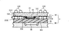
图2所示为本发明系统化构装结构的剖面示意图。如图2所示,本发明具有防球垫污染结构的系统化构装1,包括一第一封装体10与一第二封装体20,该第一封装体10具有一载板11,该载板11具有一上表面111,上表面111具有若干个球垫1111及一防焊层(未图示),其中防焊层曝露出球垫1111,在球垫1111上植入若干个焊球1112,并且在每一球垫1111外围形成至少一个凹槽112,凹槽112最佳形成在防焊层上,并且上表面111封装有至少一个与载板11电性连接的半导体芯片12。该第一封装体10的载板11上表面111上的该凹槽112环绕第一封装体10的每一球垫1111。而第二封装体20同样具有一载板21,载板21具有一上表面211及与其相对的一背面212,该上表面211封装有至少一个与其电性连接的半导体芯片22,而该背面212具有与第一封装体10上表面111上的焊球1112相对并且互相焊连的若干个焊球2121(图5C),使第二封装体20与第一封装体10形成上下堆叠的结构。其中第一封装体10相异于上表面111的另一表面上具有与其电性连接的若干个焊球113。并且第一封装体10的载板11的半导体芯片12与第二封装体20的载板21的半导体芯片22为相同或不同功能的半导体芯片。Fig. 2 is a schematic cross-sectional view of the systemized construction structure of the present invention. As shown in FIG. 2 , the
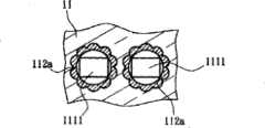
图3A与图3B所示分别为沿图2的A-A剖面线所得的球垫外凹槽的移转剖视图,以及第一封装体的不规则凹槽示意图。如图3A所示,其中第一封装体10的载板11的上表面111上的凹槽112截面形状为规则的几何形状,以本实施例而言,该凹槽112为圆形凹槽。如图3B所示,其中第一封装体10的载板11上表面111的凹槽112a截面形状为不规则的几何形状,以本实施例而言,该凹槽112a为如花瓣形凹槽。同样地,也可在第二封装体中,在球垫的周围设置凹槽,用以防止球垫被异物污染。FIG. 3A and FIG. 3B are respectively a transfer cross-sectional view of the outer groove of the ball pad taken along the section line A-A of FIG. 2 and a schematic diagram of the irregular groove of the first package. As shown in FIG. 3A , the cross-sectional shape of the
图4所示为第一封装体利用封胶封合的示意图。如图4所示,当半导体芯片12完成电性连接于载板11后,接下来便进行封胶封合制程。当封合时,如有部份的封胶13溢出时,便可流入到球垫1111周围的凹槽112中,而避免封胶13流到球垫1111上,从而可防止球垫1111被封胶13污染。这样,第一封装体10进行植入焊球时,便可减少因球垫1111污染而植球失败,从而提高制程良率。FIG. 4 is a schematic diagram of sealing the first package with glue. As shown in FIG. 4 , after the
图5A至图5D所示为本发明实施例的系统化构装结构制造方法的剖面示意图。本发明的一种具有防球垫污染结构的系统化构装制造方法,包括下列步骤:5A to 5D are schematic cross-sectional views of the manufacturing method of the systematic assembly structure according to the embodiment of the present invention. A method for systematically constructing and manufacturing an anti-pollution pad structure of the present invention comprises the following steps:
如图5A所示,首先提供一构装体,该构装体具有一载板11,该载板11具有一上表面111,该上表面111具有若干个球垫1111并具有至少一个半导体芯片12与该载板11电性连接,并在每一球垫1111外围形成至少一个凹槽112;如图5B所示,接下来形成一第一封装体10,该第一封装体10通过以一封胶13封合构装体的半导体芯片12及其上表面111的电性接合区域而形成;如图5C所示,随后提供一第二封装体20,该第二封装体20具有一载板21,该载板21具有一上表面211及一背面212,上表面211封装有至少一个与该载板21电性连接的半导体芯片22,而背面212具有植入的若干个焊球2121,并且在焊球2121上涂布助焊剂30;并且堆叠第一封装体10及第二封装体20,使第一封装体10的焊球1112与第二封装体20的焊球2121相对组接;以及,如图5D所示,最后进行回焊制程以电性接合第一封装体10与第二封装体20。As shown in FIG. 5A , a structure is provided first, the structure has a
该第一封装体10的载板11上表面111上的凹槽112截面形状为规则的几何形状或不规则的几何形状。The cross-sectional shape of the
其中第一封装体10的载板11的半导体芯片12与第二封装体20的载板21的半导体芯片22为相同或不同功能的半导体芯片。The
因此,与现有技术相比,本发明具有防球垫污染结构的系统化构装及其制造方法,通过在球垫周围形成凹槽,用以容置溢出的封胶,可避免封胶污染球垫。Therefore, compared with the prior art, the present invention has a systematic construction of an anti-pollution structure of the ball pad and its manufacturing method. By forming a groove around the ball pad to accommodate the overflowing sealant, the sealant pollution can be avoided. ball cushion.
Claims (10)
Priority Applications (1)
| Application Number | Priority Date | Filing Date | Title |
|---|---|---|---|
| CN2007100888910ACN101281900B (en) | 2007-04-04 | 2007-04-04 | Systematic package with structure for preventing solder ball pad from being contaminated and manufacturing method thereof |
Applications Claiming Priority (1)
| Application Number | Priority Date | Filing Date | Title |
|---|---|---|---|
| CN2007100888910ACN101281900B (en) | 2007-04-04 | 2007-04-04 | Systematic package with structure for preventing solder ball pad from being contaminated and manufacturing method thereof |
Publications (2)
| Publication Number | Publication Date |
|---|---|
| CN101281900Atrue CN101281900A (en) | 2008-10-08 |
| CN101281900B CN101281900B (en) | 2010-11-24 |
Family
ID=40014283
Family Applications (1)
| Application Number | Title | Priority Date | Filing Date |
|---|---|---|---|
| CN2007100888910AActiveCN101281900B (en) | 2007-04-04 | 2007-04-04 | Systematic package with structure for preventing solder ball pad from being contaminated and manufacturing method thereof |
Country Status (1)
| Country | Link |
|---|---|
| CN (1) | CN101281900B (en) |
Cited By (3)
| Publication number | Priority date | Publication date | Assignee | Title |
|---|---|---|---|---|
| CN102157453A (en)* | 2011-01-17 | 2011-08-17 | 日月光半导体制造股份有限公司 | Stacked packaging structure and manufacturing method thereof |
| CN105244292A (en)* | 2015-11-04 | 2016-01-13 | 上海凯虹电子有限公司 | Plastic packaging mould with irregular-shaped tooth sockets and method for removing excessive glue |
| WO2018126336A1 (en)* | 2017-01-03 | 2018-07-12 | 深圳市汇顶科技股份有限公司 | Substrate structure for packaging chip |
Family Cites Families (2)
| Publication number | Priority date | Publication date | Assignee | Title |
|---|---|---|---|---|
| US6093969A (en)* | 1999-05-15 | 2000-07-25 | Lin; Paul T. | Face-to-face (FTF) stacked assembly of substrate-on-bare-chip (SOBC) modules |
| CN2567768Y (en)* | 2002-08-22 | 2003-08-20 | 南茂科技股份有限公司 | Substrate-on-wafer packaging structure |
- 2007
- 2007-04-04CNCN2007100888910Apatent/CN101281900B/enactiveActive
Cited By (5)
| Publication number | Priority date | Publication date | Assignee | Title |
|---|---|---|---|---|
| CN102157453A (en)* | 2011-01-17 | 2011-08-17 | 日月光半导体制造股份有限公司 | Stacked packaging structure and manufacturing method thereof |
| CN102157453B (en)* | 2011-01-17 | 2013-08-28 | 日月光半导体制造股份有限公司 | Stacked packaging structure and manufacturing method thereof |
| CN105244292A (en)* | 2015-11-04 | 2016-01-13 | 上海凯虹电子有限公司 | Plastic packaging mould with irregular-shaped tooth sockets and method for removing excessive glue |
| CN105244292B (en)* | 2015-11-04 | 2018-07-20 | 上海凯虹电子有限公司 | The method of plastic package die and removal excessive glue with irregular shape tooth socket |
| WO2018126336A1 (en)* | 2017-01-03 | 2018-07-12 | 深圳市汇顶科技股份有限公司 | Substrate structure for packaging chip |
Also Published As
| Publication number | Publication date |
|---|---|
| CN101281900B (en) | 2010-11-24 |
Similar Documents
| Publication | Publication Date | Title |
|---|---|---|
| JP5566161B2 (en) | Package-on-package for suppressing circuit pattern floating phenomenon and manufacturing method thereof | |
| US7019407B2 (en) | Flip chip package structure | |
| JP5579402B2 (en) | Semiconductor device, method for manufacturing the same, and electronic device | |
| TWI529851B (en) | Manufacturing method of semiconductor device | |
| CN103515362A (en) | Package on package device and method of packaging semiconductor die | |
| JP2008159956A (en) | Substrate incorporating electronic component | |
| KR102574011B1 (en) | Mounting structure of semiconductor device and combination of semiconductor device and substrate | |
| TW201248808A (en) | Semiconductor device and manufacturing method thereof, and semiconductor module using the same | |
| JP2014007228A (en) | Semiconductor device and manufacturing method of the same | |
| JP2015005637A (en) | Semiconductor device | |
| US8008765B2 (en) | Semiconductor package having adhesive layer and method of manufacturing the same | |
| US20090127705A1 (en) | Semiconductor chip, method of manufacturing semiconductor chip, and semiconductor device | |
| CN100470792C (en) | Heat dissipation type three-dimensional packaging structure and manufacturing method thereof | |
| US20020093093A1 (en) | Semiconductor package with stacked dies | |
| TW201507098A (en) | Semiconductor device and method for manufacturing the same | |
| CN101281900A (en) | Systematic structure with anti-ball pad pollution structure and manufacturing method thereof | |
| CN105428251A (en) | Stacked packaging method for semiconductor | |
| JP5547703B2 (en) | Manufacturing method of semiconductor device | |
| KR20120042240A (en) | Method for producing a tmv package-on-package | |
| JP2007042762A (en) | Semiconductor device and its mounting body | |
| TWI447821B (en) | Mounting substrate and electronic device | |
| JP2009099816A (en) | Semiconductor device, method for manufacturing the same, and method for mounting the semiconductor device | |
| JP2010147225A (en) | Semiconductor device and its manufacturing method | |
| JP2008277457A (en) | Multilayer semiconductor device and mounting body | |
| JP2003158215A (en) | Semiconductor device and manufacturing method thereof |
Legal Events
| Date | Code | Title | Description |
|---|---|---|---|
| C06 | Publication | ||
| PB01 | Publication | ||
| C10 | Entry into substantive examination | ||
| SE01 | Entry into force of request for substantive examination | ||
| C14 | Grant of patent or utility model | ||
| GR01 | Patent grant |