CN101281895A - Electric connection structure with semiconductor chip embedded in circuit board - Google Patents
Electric connection structure with semiconductor chip embedded in circuit boardDownload PDFInfo
- Publication number
- CN101281895A CN101281895ACNA2007100922377ACN200710092237ACN101281895ACN 101281895 ACN101281895 ACN 101281895ACN A2007100922377 ACNA2007100922377 ACN A2007100922377ACN 200710092237 ACN200710092237 ACN 200710092237ACN 101281895 ACN101281895 ACN 101281895A
- Authority
- CN
- China
- Prior art keywords
- layer
- circuit
- semiconductor chip
- circuit board
- dielectric layer
- Prior art date
- Legal status (The legal status is an assumption and is not a legal conclusion. Google has not performed a legal analysis and makes no representation as to the accuracy of the status listed.)
- Granted
Links
Images


Classifications
- H—ELECTRICITY
- H01—ELECTRIC ELEMENTS
- H01L—SEMICONDUCTOR DEVICES NOT COVERED BY CLASS H10
- H01L24/00—Arrangements for connecting or disconnecting semiconductor or solid-state bodies; Methods or apparatus related thereto
- H01L24/01—Means for bonding being attached to, or being formed on, the surface to be connected, e.g. chip-to-package, die-attach, "first-level" interconnects; Manufacturing methods related thereto
- H01L24/18—High density interconnect [HDI] connectors; Manufacturing methods related thereto
- H01L24/19—Manufacturing methods of high density interconnect preforms
- H—ELECTRICITY
- H01—ELECTRIC ELEMENTS
- H01L—SEMICONDUCTOR DEVICES NOT COVERED BY CLASS H10
- H01L2224/00—Indexing scheme for arrangements for connecting or disconnecting semiconductor or solid-state bodies and methods related thereto as covered by H01L24/00
- H01L2224/01—Means for bonding being attached to, or being formed on, the surface to be connected, e.g. chip-to-package, die-attach, "first-level" interconnects; Manufacturing methods related thereto
- H01L2224/02—Bonding areas; Manufacturing methods related thereto
- H01L2224/04—Structure, shape, material or disposition of the bonding areas prior to the connecting process
- H01L2224/04105—Bonding areas formed on an encapsulation of the semiconductor or solid-state body, e.g. bonding areas on chip-scale packages
- H—ELECTRICITY
- H01—ELECTRIC ELEMENTS
- H01L—SEMICONDUCTOR DEVICES NOT COVERED BY CLASS H10
- H01L2224/00—Indexing scheme for arrangements for connecting or disconnecting semiconductor or solid-state bodies and methods related thereto as covered by H01L24/00
- H01L2224/01—Means for bonding being attached to, or being formed on, the surface to be connected, e.g. chip-to-package, die-attach, "first-level" interconnects; Manufacturing methods related thereto
- H01L2224/10—Bump connectors; Manufacturing methods related thereto
- H01L2224/12—Structure, shape, material or disposition of the bump connectors prior to the connecting process
- H01L2224/12105—Bump connectors formed on an encapsulation of the semiconductor or solid-state body, e.g. bumps on chip-scale packages
- H—ELECTRICITY
- H01—ELECTRIC ELEMENTS
- H01L—SEMICONDUCTOR DEVICES NOT COVERED BY CLASS H10
- H01L2224/00—Indexing scheme for arrangements for connecting or disconnecting semiconductor or solid-state bodies and methods related thereto as covered by H01L24/00
- H01L2224/01—Means for bonding being attached to, or being formed on, the surface to be connected, e.g. chip-to-package, die-attach, "first-level" interconnects; Manufacturing methods related thereto
- H01L2224/18—High density interconnect [HDI] connectors; Manufacturing methods related thereto
- H01L2224/19—Manufacturing methods of high density interconnect preforms
- H—ELECTRICITY
- H01—ELECTRIC ELEMENTS
- H01L—SEMICONDUCTOR DEVICES NOT COVERED BY CLASS H10
- H01L2224/00—Indexing scheme for arrangements for connecting or disconnecting semiconductor or solid-state bodies and methods related thereto as covered by H01L24/00
- H01L2224/73—Means for bonding being of different types provided for in two or more of groups H01L2224/10, H01L2224/18, H01L2224/26, H01L2224/34, H01L2224/42, H01L2224/50, H01L2224/63, H01L2224/71
- H01L2224/732—Location after the connecting process
- H01L2224/73251—Location after the connecting process on different surfaces
- H01L2224/73267—Layer and HDI connectors
- H—ELECTRICITY
- H01—ELECTRIC ELEMENTS
- H01L—SEMICONDUCTOR DEVICES NOT COVERED BY CLASS H10
- H01L2924/00—Indexing scheme for arrangements or methods for connecting or disconnecting semiconductor or solid-state bodies as covered by H01L24/00
- H01L2924/15—Details of package parts other than the semiconductor or other solid state devices to be connected
- H01L2924/151—Die mounting substrate
- H01L2924/1515—Shape
- H01L2924/15153—Shape the die mounting substrate comprising a recess for hosting the device
- H—ELECTRICITY
- H01—ELECTRIC ELEMENTS
- H01L—SEMICONDUCTOR DEVICES NOT COVERED BY CLASS H10
- H01L2924/00—Indexing scheme for arrangements or methods for connecting or disconnecting semiconductor or solid-state bodies as covered by H01L24/00
- H01L2924/15—Details of package parts other than the semiconductor or other solid state devices to be connected
- H01L2924/181—Encapsulation
- H01L2924/1815—Shape
- H01L2924/1816—Exposing the passive side of the semiconductor or solid-state body
- H01L2924/18162—Exposing the passive side of the semiconductor or solid-state body of a chip with build-up interconnect
- H—ELECTRICITY
- H01—ELECTRIC ELEMENTS
- H01L—SEMICONDUCTOR DEVICES NOT COVERED BY CLASS H10
- H01L2924/00—Indexing scheme for arrangements or methods for connecting or disconnecting semiconductor or solid-state bodies as covered by H01L24/00
- H01L2924/30—Technical effects
- H01L2924/35—Mechanical effects
- H01L2924/351—Thermal stress
Landscapes
- Engineering & Computer Science (AREA)
- Manufacturing & Machinery (AREA)
- Computer Hardware Design (AREA)
- Microelectronics & Electronic Packaging (AREA)
- Power Engineering (AREA)
- Structures For Mounting Electric Components On Printed Circuit Boards (AREA)
Abstract
Translated fromChinese
Description
Translated fromChinese技术领域technical field
本发明涉及一种嵌埋半导体芯片的电路板结构,尤指一种用以电性连接埋入支承板的半导体芯片与线路的空心导电盲孔结构。The invention relates to a circuit board structure for embedding a semiconductor chip, in particular to a hollow conductive blind hole structure for electrically connecting the semiconductor chip embedded in a supporting board and a circuit.
背景技术Background technique
随着半导体封装技术的发展,半导体装置(Semiconductor device)已开发出不同的封装型态,其主要是在一封装基板(package substrate)或导线架上先装置半导体芯片,再将半导体芯片电性连接在该封装基板或导线架上,接着以胶体进行封装。其中球栅阵列式(Ball gridarray,BGA)为一种先进的半导体封装技术,其特点在于采用一封装基板来安置半导体芯片,并利用自动对位(Self-alignment)技术以于该封装基板背面植置多个成栅状阵列排列的锡球(Solder ball),使相同单位面积的半导体芯片承载件上可以容纳更多输入/输出连接端(I/Oconnection)以符合高度集成化(Integration)的半导体芯片所需,以通过该些锡球以电性连接至外部装置。With the development of semiconductor packaging technology, different packaging types have been developed for semiconductor devices, which mainly install semiconductor chips on a package substrate or lead frame first, and then electrically connect the semiconductor chips On the packaging substrate or lead frame, encapsulation is then performed with glue. Among them, ball grid array (Ball grid array, BGA) is an advanced semiconductor packaging technology. Place a plurality of solder balls arranged in a grid array, so that more input/output connection terminals (I/Oconnection) can be accommodated on the semiconductor chip carrier of the same unit area to meet the requirements of highly integrated semiconductors. The chip needs to be electrically connected to external devices through these solder balls.
但是现有的半导体封装结构是将半导体芯片黏贴于基板顶面,进行打线接合(wire bonding)或覆晶接合(Flip chip)封装,再于基板的背面植以锡球以进行电性连接,如此,虽可达到高脚数的目的,但是在更高频使用时或高速操作时,其将因导线连接路径过长而产生电气特性的效能无法提升,而有所限制。另外,因传统封装需要多次的连接接口,相对地增加制造的复杂度。However, the existing semiconductor packaging structure is to paste the semiconductor chip on the top surface of the substrate, perform wire bonding (wire bonding) or flip chip bonding (Flip chip) packaging, and then plant solder balls on the back of the substrate for electrical connection. In this way, although the purpose of high pin count can be achieved, when it is used at a higher frequency or at a high speed, it will be limited due to the fact that the performance of the electrical characteristics cannot be improved due to the long connection path of the wire. In addition, because traditional packaging requires multiple connection interfaces, the complexity of manufacturing is relatively increased.
鉴此,为了能有效地提升电性质量而符合下世代产品的应用,业界纷纷研究采用将芯片埋入封装基板内以直接的电性连接,用以缩短电性传导路径,并可减少信号损失、信号失真及提升高速操作的能力。In view of this, in order to effectively improve the electrical quality and meet the application of next-generation products, the industry has been researching to embed the chip in the packaging substrate for direct electrical connection, so as to shorten the electrical conduction path and reduce signal loss. , signal distortion and the ability to improve high-speed operation.
如图1所示,为现有的半导体组件埋入基板的封装件的剖面示意图。如图所示,该封装件包括承载板10,且该承载板10的一表面100形成有至少一开口100a;至少一半导体芯片11,且该半导体芯片11上形成有多个电极垫110,接置于该承载板10上且收纳于该开口100a中;一线路增层结构12形成于该承载板10上,且该线路增层结构12通过多个导电盲孔120电性连接至该半导体芯片11上的电极垫110。As shown in FIG. 1 , it is a schematic cross-sectional view of a conventional semiconductor package embedded in a substrate. As shown in the figure, the package includes a
该半导体芯片11具有一主动面11a及与该主动面相对的非主动面11b,且该主动面11a上形成有多个电极垫110,该非主动面11b通过胶黏剂13接置于该承载板开口100a中。The
该线路增层结构12包括至少一介电层121,与该介电层121交错叠置的线路层122,以及贯穿该介电层121以电性连接该线路层122的导电盲孔120,且所述多个导电盲孔120得以电性连接至该半导体芯片11的电极垫110。而在该线路增层结构12的最外表面的线路层上则形成有多个电性连接端123,且该最外层线路层上形成有一防焊层124,而该防焊层124具有多个开孔以外露出该电性连接端123,用以提供植置有导电组件,例如为焊球125(Solder ball),从而供收纳于该承载板10中的该半导体芯片11得以通过其表面的电极垫110、该线路增层结构12以及该焊球125电性导接至外部组件。The wiring build-up structure 12 includes at least one dielectric layer 121, wiring layers 122 stacked alternately with the dielectric layer 121, and conductive
如上所述,现有的芯片埋入式封装结构中,该线路层通过导电盲孔直接与半导体芯片作电性连接,而该导电盲孔系通过于形成于绝缘层中的盲孔(Via)中电镀铜形成,且铜材料填满该盲孔。然,由于所形成的导电盲孔周围的各组成组件(例如绝缘层、半导体芯片表面的保护层等)的热膨胀系数(Coeffecient Thermal Efficent;CTE)不匹配,导致所形成的半导体封装件由于各组成组件之间的热膨胀差异,而于该半导体封装件中产生热应力,进而可能导致所形成的线路结构与半导体芯片的电极垫表面产生分离而导致产品电性失效。As mentioned above, in the existing chip-embedded packaging structure, the circuit layer is directly electrically connected to the semiconductor chip through the conductive blind hole, and the conductive blind hole is formed in the insulating layer through the blind hole (Via) Electroplated copper is formed, and the copper material fills the blind hole. However, due to the thermal expansion coefficient (Coeffecient Thermal Efficent; CTE) mismatch of the components around the formed conductive blind vias (such as the insulating layer, the protective layer on the surface of the semiconductor chip, etc.), the semiconductor package formed due to various components The difference in thermal expansion between the components will generate thermal stress in the semiconductor package, which may lead to the separation of the formed circuit structure and the surface of the electrode pad of the semiconductor chip, resulting in electrical failure of the product.
又现有的半导体封装件中,为满足细线路(Fine Pitch)的要求及所短信号传导路径,与线路连接的导电盲孔采用叠置结构,然而由于该导电盲孔周围的各组成组件,例如绝缘层、半导体芯片表面的保护层等的热膨胀系数各不相同,导致产品内部产生的热应力不匹配,而使该半导体芯片的电极垫与线路结构之间产生分离,故无法满足细线路的要求,同时亦影响产品的信赖度。In the existing semiconductor package, in order to meet the requirements of the fine pitch (Fine Pitch) and the short signal conduction path, the conductive blind holes connected to the circuit adopt a stacked structure. However, due to the components around the conductive blind holes, For example, the thermal expansion coefficients of the insulating layer and the protective layer on the surface of the semiconductor chip are different, resulting in a mismatch of thermal stress generated inside the product, and the separation between the electrode pad and the circuit structure of the semiconductor chip, so it cannot meet the requirements of thin lines. Requirements, but also affect the reliability of the product.
因此,如何提出一种电路板嵌埋有半导体芯片的电性连接结构,以避免现有技术的种种缺失,实已成为目前业界亟待解决的技术问题。Therefore, how to propose an electrical connection structure in which a semiconductor chip is embedded in a circuit board to avoid various deficiencies in the prior art has become an urgent technical problem in the industry.
发明内容Contents of the invention
鉴于上述现有技术的种种缺失,本发明的主要目的在于提供一种嵌埋半导体芯片的电路板结构,以提升产品电性能,避免半导体芯片的电极垫与增层线路结构之间产生分离。In view of the deficiencies of the above-mentioned prior art, the main purpose of the present invention is to provide a circuit board structure for embedding semiconductor chips to improve the electrical performance of the product and avoid separation between the electrode pads of the semiconductor chip and the build-up circuit structure.
本发明的又一目的在于提供一种嵌埋半导体芯片的电路板结构,以提升产品优良率及产品的信赖度。Another object of the present invention is to provide a circuit board structure embedded with semiconductor chips, so as to improve product yield and product reliability.
本发明的再一目的在于提供一种嵌埋半导体芯片的电路板结构,以缩短电性传导路径且增加线路布局的弹性。Another object of the present invention is to provide a circuit board structure for embedding semiconductor chips, so as to shorten the electrical conduction path and increase the flexibility of circuit layout.
为达上述及其它目的,本发明提出一种嵌埋半导体芯片的电路板结构,包括:一支承板,其具有至少一开口;至少一半导体芯片,其嵌埋于该支承板的开口中,该半导体芯片具有一主动面,且该主动面具有多个电极垫;芯面保护层,其形成于该半导体芯片的主动面,且该芯面保护层具有相对于该电极垫的开孔,以显露出该半导体芯片的电极垫;金属层,其形成于露出该芯面保护层开孔的电极垫上;介电层,其形成于该支承板及芯面保护层表面,且该介电层形成有相对于该电极垫的开孔,以露出该半导体芯片的电极垫;以及线路层,其形成于该介电层的表面,并于该介电层的开孔中形成有与该线路层电性连接的空心导电盲孔,以供该线路层得以通过该空心导电盲孔电性连接至该半导体芯片的电极垫上的金属层。To achieve the above and other purposes, the present invention proposes a circuit board structure for embedding semiconductor chips, comprising: a support plate having at least one opening; at least one semiconductor chip embedded in the opening of the support plate, the The semiconductor chip has an active surface, and the active surface has a plurality of electrode pads; the core surface protection layer is formed on the active surface of the semiconductor chip, and the core surface protection layer has openings relative to the electrode pads to expose The electrode pads of the semiconductor chip; the metal layer, which is formed on the electrode pads exposing the openings of the core surface protection layer; the dielectric layer, which is formed on the surface of the support plate and the core surface protection layer, and the dielectric layer is formed with Relative to the opening of the electrode pad, to expose the electrode pad of the semiconductor chip; and a wiring layer, which is formed on the surface of the dielectric layer, and is formed in the opening of the dielectric layer to be electrically connected to the wiring layer. The connected hollow conductive blind hole is used for the circuit layer to be electrically connected to the metal layer on the electrode pad of the semiconductor chip through the hollow conductive blind hole.
于本发明的另一实施例中,上述金属层与空心导电盲孔之间还具有一缓冲金属层。In another embodiment of the present invention, there is a buffer metal layer between the metal layer and the hollow conductive blind hole.
于本发明的再一实施例中,该嵌埋半导体芯片的电路板结构还包括一形成于该介电层及线路层表面线路增层结构,且该线路增层结构中形成有多个满镀金属盲孔以电性连接至该线路层,并于该线路增层结构表面形成有电性连接垫。该线路增层结构包括有至少一介电层、叠置于该介电层上的线路层,以及形成于该介电层中的满镀金属盲孔。此外,该线路增层结构表面具有防焊层,且该防焊层具有多个开孔,以显露线路增层结构表面的电性连接垫。In yet another embodiment of the present invention, the circuit board structure for embedding semiconductor chips further includes a circuit build-up structure formed on the surface of the dielectric layer and the circuit layer, and a plurality of full plating layers are formed in the circuit build-up structure. The metal blind hole is electrically connected to the wiring layer, and an electrical connection pad is formed on the surface of the wiring build-up structure. The circuit build-up structure includes at least one dielectric layer, a circuit layer stacked on the dielectric layer, and a fully plated metal blind hole formed in the dielectric layer. In addition, the surface of the circuit build-up structure has a solder resist layer, and the solder resist layer has a plurality of openings to expose the electrical connection pads on the surface of the circuit build-up structure.
于本发明的又一实施例中,上述线路增层结构中的满镀金属盲孔是延伸至该线路层的空心导电盲孔的底部。In yet another embodiment of the present invention, the fully plated blind vias in the circuit layer build-up structure extend to the bottom of the hollow conductive blind vias in the circuit layer.
相比于现有技术,本发明的嵌埋半导体芯片的电路板结构,主要是在绝缘层中形成空心导电盲孔以供形成于该绝缘层表面的线路层电性连接至埋设于支承板开口中的半导体芯片的电极垫。本发明可通过该空心导电盲孔中的介电层与形成于空心导电盲孔外围的介电层可解决热膨胀系数不易匹配的问题,且空心导电盲孔内外介电层材料相同,可降低其应力,而可避免半导体芯片与其上形成的增层线路分离,进而使产品的电性质量降低的缺失。Compared with the prior art, the circuit board structure for embedding semiconductor chips of the present invention mainly forms hollow conductive blind holes in the insulating layer for electrically connecting the circuit layer formed on the surface of the insulating layer to the opening embedded in the support plate electrode pads in a semiconductor chip. The present invention can solve the problem that the coefficient of thermal expansion is not easy to match through the dielectric layer in the hollow conductive blind hole and the dielectric layer formed on the periphery of the hollow conductive blind hole, and the material of the inner and outer dielectric layers of the hollow conductive blind hole is the same, which can reduce its Stress can avoid the separation of the semiconductor chip and the build-up circuit formed on it, thereby reducing the electrical quality of the product.
又,本发明中,可于上述介电层及线路层上继续进行线路增层制造以形成线路增层结构,且该线路增层结构的满镀金属盲孔可延伸至该线路层的空心导电盲孔底部以形成叠置的盲孔结构,因而可应用于细线路电路板中,同时可缩短电性传导路径、增加线路布局的弹性。Also, in the present invention, the line build-up manufacturing can be continued on the above-mentioned dielectric layer and circuit layer to form a line build-up structure, and the fully plated metal blind holes of the line build-up structure can extend to the hollow conductive holes of the line layer. The bottom of the blind hole forms a stacked blind hole structure, so it can be applied to a thin circuit board, and at the same time can shorten the electrical conduction path and increase the flexibility of the circuit layout.
附图说明Description of drawings
图1为显示现有芯片埋入基板的封装件的剖面示意图;FIG. 1 is a schematic cross-sectional view showing a conventional chip-embedded substrate package;
图2为显示本发明的嵌埋半导体芯片的电路板结构第一实施例的剖面示意图;2 is a schematic cross-sectional view showing a first embodiment of a circuit board structure for embedding semiconductor chips of the present invention;
图3为显示本发明的嵌埋半导体芯片的电路板结构第二实施例的剖面示意图;3 is a schematic cross-sectional view showing a second embodiment of a circuit board structure for embedding semiconductor chips of the present invention;
图4为显示本发明的嵌埋半导体芯片的电路板结构第三实施例的剖面示意图;4 is a schematic cross-sectional view showing a third embodiment of a circuit board structure for embedding semiconductor chips of the present invention;
图5为显示本发明的嵌埋半导体芯片的电路板结构第四实施例的剖面示意图;5 is a schematic cross-sectional view showing a fourth embodiment of a circuit board structure for embedding semiconductor chips of the present invention;
图6为显示本发明的嵌埋半导体芯片的电路板结构第五实施例的剖面示意图;以及6 is a schematic cross-sectional view showing a fifth embodiment of the circuit board structure for embedding semiconductor chips of the present invention; and
图7为显示本发明的嵌埋半导体芯片的电路板结构第六实施例的剖面示意图。7 is a schematic cross-sectional view showing a sixth embodiment of the circuit board structure for embedding semiconductor chips of the present invention.
附图标记说明Explanation of reference signs
10 承载板10 load board
100 表面100 surface
100a,200开口100a, 200 openings
11,21 半导体芯片11, 21 Semiconductor chips
123 电性连接垫123 Electrical connection pad
11a 主动面11a Active face
11b 非主动面11b passive surface
12,40 线路增层结构12, 40 Line build-up structure
120 导电盲孔120 Conductive blind vias
121,24,400介电层121, 24, 400 dielectric layer
122,25,402线路层122, 25, 402 line layer
125 焊球125 solder balls
13 胶黏剂13 Adhesive
20 支承板20 Support plate
110,210 电极垫110, 210 electrode pads
21a 主动面21a Active face
21b 非主动面21b passive surface
220,240 开孔220, 240 opening
22 芯面保护层22 Core protective layer
23 金属层23 metal layer
250 空心导电盲孔250 Hollow Conductive Blind Vias
26,124 防焊层26, 124 Solder mask
30 缓冲金属层30 buffer metal layer
404,406 满镀金属盲孔404, 406 fully plated metal blind hole
具体实施方式Detailed ways
以下通过特定的具体实施例说明本发明的实施方式,熟悉此技艺的人士可由本说明书所揭示的内容轻易地了解本发明的其它优点与功效。本发明亦可通过其它不同的具体实施例加以施行或应用,本说明书中的各项细节亦可基于不同观点与应用,在不背离本发明的精神下进行各种修饰与变更。The implementation of the present invention is described below through specific examples, and those skilled in the art can easily understand other advantages and effects of the present invention from the content disclosed in this specification. The present invention can also be implemented or applied through other different specific embodiments, and various modifications and changes can be made to the details in this specification based on different viewpoints and applications without departing from the spirit of the present invention.
第一实施例first embodiment
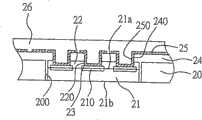
如图2所示为本发明的嵌埋半导体芯片的电路板结构第一实施例的剖面示意图。如图所示,本发明的嵌埋半导体芯片的电路板结构包括:一支承板20、至少一半导体芯片21、芯面保护层22、金属层23、介电层24、线路层25以及空心导电盲孔250。FIG. 2 is a schematic cross-sectional view of a first embodiment of a circuit board structure for embedding semiconductor chips according to the present invention. As shown in the figure, the circuit board structure of the embedded semiconductor chip of the present invention includes: a
上述支承板20可为完成前段线路制造的电路板、绝缘板或为一核心板,且该核心板的材质可为金属或非金属。又该支承板20中形成有至少一开口200以收纳该半导体芯片21。The
该半导体芯片21具有一主动面21a及相对的非主动面21b,且该主动面21a上形成有多个电极垫210。The
该芯面保护层22形成于半导体芯片21的主动面21a上,且该芯面保护层22中对应半导体芯片21的电极垫210的位置形成有开孔220以显露出该些电极垫210。The
该金属层23形成于芯面保护层22的开孔220中的电极垫210表面上,而该金属层23可为金属阻障层(under Bump metallization;UBM),例如为镍/金金属层,通过该金属层23以保护覆盖在其下的电极垫210。The
该介电层24形成于该支承板20及半导体片21的主动面21a,且该介电层24形成有相对于电极垫210的开孔240,以显露出该半导体芯片21的电极垫210。其中,该介电层24可例如为环氧树脂(Epoxyresin)、聚乙酰胺(Polyimide)、氰脂(Cyanate ester)、玻璃纤维(Glassfiber)、双顺丁烯二酸酰亚胺/三氮阱(BT,Bismaleimide triazine)或混合环氧树脂与玻璃纤维等材质构成。The
该线路层25形成于该介电层24的表面,并于该介电层24的开孔240中形成有与该线路层25电性连接的空心导电盲孔250,以供该线路层25通过该空心导电盲孔250而电性连接至该半导体芯片21的电极垫210。上述线路层25例如为图案化铜层,其制作方法种类繁多且为业界所现有,故在此不再为文赘述。The
此外,本发明的结构还包括一防焊层26,于该防焊层26中形成多个开孔(图未示)以露出该线路层25中作为电性连接垫部分(图未示),且该防焊层26填满该空心导电盲孔250。之后可于该电性连接垫上接置导电组件(例如为焊球)以完成半导体芯片21向外的电性连接。In addition, the structure of the present invention also includes a solder resist
本发明的嵌埋半导体芯片的电路板结构主要特征为介电层24的开孔中形成的导电结构为空心导电盲孔250,从而可通过该空心导电盲孔使其周围的介电层、防焊层、芯面保护层的热膨胀系数(CTE)相匹配,以降低产品内部产生的热应力,进而避免埋设于该电路板中的半导体芯片的电极垫与形成于其上的线路层产生分离,导致产品的电性失效。较佳的实施方式,为上述的防焊层、介电层、芯面保护层的材料可为热膨胀系数相近的材料,使该空心导电盲孔250的周围得有相近的膨胀系数,而可以降低产品于工作中所产生的热应力。The main feature of the circuit board structure for embedding semiconductor chips of the present invention is that the conductive structure formed in the opening of the
第二实施例second embodiment
如图3所示为本发明的嵌埋半导体芯片的电路板结构第二实施例的剖面示意图。FIG. 3 is a schematic cross-sectional view of a second embodiment of a circuit board structure for embedding semiconductor chips according to the present invention.
本实施例中该嵌埋半导体芯片的电路板结构与前述第一实施例大致相同,其主要差异在于本实施例还包括一缓冲金属层。The structure of the circuit board embedded with semiconductor chips in this embodiment is substantially the same as that of the first embodiment, the main difference is that this embodiment further includes a buffer metal layer.
如图3所示,一缓冲金属层30形成于上述的空心导电盲孔250及金属层23之间,而该缓冲金属层30可为铜箔,以便于该金属层23厚度不足时,通过该增厚的缓冲金属层30作为后续介电层24形成开孔(即盲孔)的雷射开孔制造的挡止层,进而防止覆盖在其下的半导体芯片21的电极垫210受到损坏。As shown in Figure 3, a
第三实施例third embodiment
如图4所示为本发明的嵌埋半导体芯片的电路板结构第三实施例的剖面示意图。FIG. 4 is a schematic cross-sectional view of a third embodiment of a circuit board structure embedded with semiconductor chips according to the present invention.
本实施例中该嵌埋半导体芯片的电路板结构与前述第一实施例大致相同,其主要差异在于本实施例的嵌埋半导体芯片的电路板结构还包括一形成于介电层24及线路层25表面的线路增层结构40。In this embodiment, the structure of the circuit board for embedding semiconductor chips is roughly the same as that of the aforementioned first embodiment. The circuit build-up
该线路增层结构40包括至少一介电层400、叠置于该介电层400表面上的线路层402以及形成于介电层400中以供线路层402电性连接至线路层25的满镀金属盲孔404;当然另亦可使用空心导电盲孔(图未示)当作线路层402与线路层25的电讯传导路径。The circuit build-up
上述介电层400填满空心导电盲孔250。本实施例中,通过该空心导电盲孔250的设计使其周围的介电层24,400及芯面保护层22的热膨胀系数较相匹配,因而可避免产品于工作中产生的热能,使半导体芯片的电极垫与线路层间的介电层因热膨胀问题而产生电极垫与线路层分离的现象。The
此外,本实施例中,线路增层结构40的线路层402表面还形成有多个电性连接垫(未图示),且该线路增层结构40外表面形成有一防焊层26以保护覆盖在其下的线路,并形成有多个开孔(图未示)以露出线路增层结构40表面的电性连接垫(图未示)。之后可于该电性连接垫上接置导电组件(例如为焊球)以完成半导体芯片21向外的电性连接。In addition, in this embodiment, a plurality of electrical connection pads (not shown) are formed on the surface of the
第四实施例Fourth embodiment
如图5所示为本发明的嵌埋半导体芯片的电路板结构第四实施例的剖面示意图。FIG. 5 is a schematic cross-sectional view of a fourth embodiment of a circuit board structure for embedding semiconductor chips according to the present invention.
本实施例中该嵌埋半导体芯片的电路板结构与前述第三实施例大致相同,其主要差异在于本实施例的嵌埋半导体芯片的电路板结构还包括一缓冲金属层30。The circuit board structure for embedding semiconductor chips in this embodiment is substantially the same as that of the aforementioned third embodiment, the main difference being that the circuit board structure for embedding semiconductor chips in this embodiment further includes a
如图5所示,一缓冲金属层30形成于该金属层23与空心导电盲孔250之间,而该缓冲金属层30的功用如上述第二实施例所示,于此不再赘述的。As shown in FIG. 5 , a
第五实施例fifth embodiment
如图6所示为本发明的嵌埋半导体芯片的电路板结构第五实施例的剖面示意图。FIG. 6 is a schematic cross-sectional view of a fifth embodiment of a circuit board structure for embedding semiconductor chips according to the present invention.
本实施例中该嵌埋半导体芯片的电路板结构与前述第三实施例大致相同,其主要差异在于本实施例的嵌埋半导体芯片的电路板结构中,线路增层结构40中形成有另一满镀金属盲孔406。The structure of the circuit board for embedding semiconductor chips in this embodiment is roughly the same as that of the aforementioned third embodiment, and the main difference is that in the structure of the circuit board for embedding semiconductor chips in this embodiment, another Fully plated
如图6所示,另一满镀金属盲孔406连通至该最初形成的线路层25的空心导电盲孔250的底部,以形成叠置盲孔的结构,使其可应用于细线路电路板中,并可缩短电性传导路径,以增加线路布局的弹性。As shown in FIG. 6, another fully plated metal
第六实施例Sixth embodiment
如图7所示为本发明的嵌埋半导体芯片的电路板结构第六实施例的剖面示意图。FIG. 7 is a schematic cross-sectional view of a sixth embodiment of a circuit board structure for embedding semiconductor chips according to the present invention.
本实施例中该嵌埋半导体芯片的电路板结构系与前述第五实施例大致相同,其主要差异在于本实施例的嵌埋半导体芯片的电路板结构还包括一缓冲金属层30。The circuit board structure for embedding semiconductor chips in this embodiment is substantially the same as that of the aforementioned fifth embodiment. The main difference is that the circuit board structure for embedding semiconductor chips in this embodiment further includes a
如图7所示,该缓冲金属层30形成于该金属层23与空心导电盲孔250之间,而该缓冲金属层30的功用如上述第二实施例所示,在此不再赘述的。As shown in FIG. 7 , the
因此,本发明的嵌埋半导体芯片的电路板结构,主要是将半导体芯片收纳于支承板的开口中,之后于该支承板及该半导体芯片上进行线路制造,以形成该介电层及线路层,且于该介电层中形成空心导电盲孔,以供该线路层电性连接至该半导体芯片上的电极垫。因此,本发明可通过该空心导电盲孔使其周围的组成组件,例如介电层、芯面保护层的热膨胀系数相近材料,避免空心导电盲孔中的介电层与形成于空心导电盲孔外围的介电层可解决热膨胀系数不易匹配的问题,且该空心导电盲孔内外介电层材料相同,可降低其应力,而可避免半导体芯片与其上形成的增层线路分离,进而使产品电性质量降低的缺失。Therefore, the semiconductor chip embedded circuit board structure of the present invention is mainly to accommodate the semiconductor chip in the opening of the support plate, and then perform circuit manufacturing on the support plate and the semiconductor chip to form the dielectric layer and the circuit layer. , and form a hollow conductive blind hole in the dielectric layer for the circuit layer to be electrically connected to the electrode pad on the semiconductor chip. Therefore, the present invention can make its surrounding components through the hollow conductive blind hole, such as materials with similar thermal expansion coefficients of the dielectric layer and the core surface protection layer, so as to avoid the dielectric layer in the hollow conductive blind hole from being formed in the hollow conductive blind hole. The peripheral dielectric layer can solve the problem that the thermal expansion coefficient is not easy to match, and the material of the inner and outer dielectric layers of the hollow conductive blind hole is the same, which can reduce its stress and avoid the separation of the semiconductor chip from the build-up circuit formed on it, thereby making the product electrical The absence of reduced sexual quality.
又,本发明中,可于上述的介电层及线路层上继续进行线路增层制造以形成线路增层结构,且该线路增层结构的满镀金属盲孔可延伸至该线路层的空心导电盲孔底部以形成叠置的盲孔结构,因而可应用于细线路电路板中,同时可缩短电性传导路径、增加线路布局的弹性。Also, in the present invention, the circuit build-up manufacturing can be continued on the above-mentioned dielectric layer and circuit layer to form a circuit build-up structure, and the fully plated metal blind holes of the circuit build-up structure can extend to the hollow of the circuit layer The bottom of the conductive blind hole forms a stacked blind hole structure, so it can be applied to a thin circuit circuit board, and at the same time can shorten the electrical conduction path and increase the flexibility of the circuit layout.
上述实施例仅为例示性说明本发明的原理及其功效,而非用于限制本发明。任何本领域技术人员均可在不违背本发明的精神及范畴下,对上述实施例进行修饰与变化。因此,本发明的权利保护范围,应如前述的权利要求书所列。The above-mentioned embodiments are only illustrative to illustrate the principles and effects of the present invention, and are not intended to limit the present invention. Any person skilled in the art can modify and change the above-mentioned embodiments without departing from the spirit and scope of the present invention. Therefore, the protection scope of the present invention should be as listed in the preceding claims.
Claims (7)
Translated fromChinesePriority Applications (1)
| Application Number | Priority Date | Filing Date | Title |
|---|---|---|---|
| CNB2007100922377ACN100539102C (en) | 2007-04-02 | 2007-04-02 | Electric connection structure with semiconductor chip embedded in circuit board |
Applications Claiming Priority (1)
| Application Number | Priority Date | Filing Date | Title |
|---|---|---|---|
| CNB2007100922377ACN100539102C (en) | 2007-04-02 | 2007-04-02 | Electric connection structure with semiconductor chip embedded in circuit board |
Publications (2)
| Publication Number | Publication Date |
|---|---|
| CN101281895Atrue CN101281895A (en) | 2008-10-08 |
| CN100539102C CN100539102C (en) | 2009-09-09 |
Family
ID=40014278
Family Applications (1)
| Application Number | Title | Priority Date | Filing Date |
|---|---|---|---|
| CNB2007100922377AExpired - Fee RelatedCN100539102C (en) | 2007-04-02 | 2007-04-02 | Electric connection structure with semiconductor chip embedded in circuit board |
Country Status (1)
| Country | Link |
|---|---|
| CN (1) | CN100539102C (en) |
Cited By (4)
| Publication number | Priority date | Publication date | Assignee | Title |
|---|---|---|---|---|
| CN102740597A (en)* | 2011-04-07 | 2012-10-17 | 陈群 | Manufacturing method for substrate embedded with electronic element |
| CN105990379A (en)* | 2015-02-25 | 2016-10-05 | 联想(北京)有限公司 | Photosensitive module group and manufacturing method thereof |
| CN115483116A (en)* | 2021-06-16 | 2022-12-16 | 先丰通讯股份有限公司 | Package structure and manufacturing method thereof, circuit board and manufacturing method thereof |
| CN119891990A (en)* | 2025-03-28 | 2025-04-25 | 深圳市晶扬电子有限公司 | Heterogeneous integrated filter structure with transient voltage protection and manufacturing method |
Family Cites Families (2)
| Publication number | Priority date | Publication date | Assignee | Title |
|---|---|---|---|---|
| JP4693258B2 (en)* | 2001-02-26 | 2011-06-01 | 京セラ株式会社 | Manufacturing method of multilayer wiring board |
| JP2006351565A (en)* | 2005-06-13 | 2006-12-28 | Shinko Electric Ind Co Ltd | Stacked semiconductor package |
- 2007
- 2007-04-02CNCNB2007100922377Apatent/CN100539102C/ennot_activeExpired - Fee Related
Cited By (5)
| Publication number | Priority date | Publication date | Assignee | Title |
|---|---|---|---|---|
| CN102740597A (en)* | 2011-04-07 | 2012-10-17 | 陈群 | Manufacturing method for substrate embedded with electronic element |
| CN105990379A (en)* | 2015-02-25 | 2016-10-05 | 联想(北京)有限公司 | Photosensitive module group and manufacturing method thereof |
| CN105990379B (en)* | 2015-02-25 | 2019-07-26 | 联想(北京)有限公司 | A kind of photosensitive mould group and production method |
| CN115483116A (en)* | 2021-06-16 | 2022-12-16 | 先丰通讯股份有限公司 | Package structure and manufacturing method thereof, circuit board and manufacturing method thereof |
| CN119891990A (en)* | 2025-03-28 | 2025-04-25 | 深圳市晶扬电子有限公司 | Heterogeneous integrated filter structure with transient voltage protection and manufacturing method |
Also Published As
| Publication number | Publication date |
|---|---|
| CN100539102C (en) | 2009-09-09 |
Similar Documents
| Publication | Publication Date | Title |
|---|---|---|
| TWI651828B (en) | Chip package structure and method of manufacturing same | |
| US10212818B2 (en) | Methods and apparatus for a substrate core layer | |
| US7411281B2 (en) | Integrated circuit device package having both wire bond and flip-chip interconnections and method of making the same | |
| US6951773B2 (en) | Chip packaging structure and manufacturing process thereof | |
| US7579690B2 (en) | Semiconductor package structure | |
| US9129870B2 (en) | Package structure having embedded electronic component | |
| US8159057B2 (en) | Semiconductor device and manufacturing method therefor | |
| US8580608B2 (en) | Fabrication method of package structure having embedded semiconductor component | |
| US20080157327A1 (en) | Package on package structure for semiconductor devices and method of the same | |
| US7863729B2 (en) | Circuit board structure embedded with semiconductor chips | |
| US20110031606A1 (en) | Packaging substrate having embedded semiconductor chip | |
| US8008765B2 (en) | Semiconductor package having adhesive layer and method of manufacturing the same | |
| TWI533424B (en) | Package carrier | |
| TW201947722A (en) | Flip-chip package substrate | |
| CN101425510A (en) | Laminated packaging structure of semiconductor element and method thereof | |
| CN1971894A (en) | Chip-embedded modular structure | |
| US20160104652A1 (en) | Package structure and method of fabricating the same | |
| CN101281895A (en) | Electric connection structure with semiconductor chip embedded in circuit board | |
| TWI570856B (en) | Package structure and method of manufacture | |
| KR20010063236A (en) | Stack package and manufacturing method thereof | |
| US20240096838A1 (en) | Component-embedded packaging structure | |
| TWI558286B (en) | Package structure and method of fabricating the same | |
| JP2004072113A (en) | Thermally strengthened integrated circuit package | |
| US20080174031A1 (en) | Chip package reducing wiring layers on substrate and its carrier | |
| KR20250145524A (en) | Circuit board and package substrate having the same |
Legal Events
| Date | Code | Title | Description |
|---|---|---|---|
| C06 | Publication | ||
| PB01 | Publication | ||
| C10 | Entry into substantive examination | ||
| SE01 | Entry into force of request for substantive examination | ||
| C14 | Grant of patent or utility model | ||
| GR01 | Patent grant | ||
| CF01 | Termination of patent right due to non-payment of annual fee | ||
| CF01 | Termination of patent right due to non-payment of annual fee | Granted publication date:20090909 |