CN101280161B - Conducting adhesive tape and manufacturing method thereof - Google Patents
Conducting adhesive tape and manufacturing method thereofDownload PDFInfo
- Publication number
- CN101280161B CN101280161BCN200710073979.5ACN200710073979ACN101280161BCN 101280161 BCN101280161 BCN 101280161BCN 200710073979 ACN200710073979 ACN 200710073979ACN 101280161 BCN101280161 BCN 101280161B
- Authority
- CN
- China
- Prior art keywords
- carbon nano
- carbon nanotube
- layer
- conductive tape
- tube film
- Prior art date
- Legal status (The legal status is an assumption and is not a legal conclusion. Google has not performed a legal analysis and makes no representation as to the accuracy of the status listed.)
- Active
Links
Images


Classifications
- H—ELECTRICITY
- H01—ELECTRIC ELEMENTS
- H01R—ELECTRICALLY-CONDUCTIVE CONNECTIONS; STRUCTURAL ASSOCIATIONS OF A PLURALITY OF MUTUALLY-INSULATED ELECTRICAL CONNECTING ELEMENTS; COUPLING DEVICES; CURRENT COLLECTORS
- H01R4/00—Electrically-conductive connections between two or more conductive members in direct contact, i.e. touching one another; Means for effecting or maintaining such contact; Electrically-conductive connections having two or more spaced connecting locations for conductors and using contact members penetrating insulation
- H01R4/04—Electrically-conductive connections between two or more conductive members in direct contact, i.e. touching one another; Means for effecting or maintaining such contact; Electrically-conductive connections having two or more spaced connecting locations for conductors and using contact members penetrating insulation using electrically conductive adhesives
- Y—GENERAL TAGGING OF NEW TECHNOLOGICAL DEVELOPMENTS; GENERAL TAGGING OF CROSS-SECTIONAL TECHNOLOGIES SPANNING OVER SEVERAL SECTIONS OF THE IPC; TECHNICAL SUBJECTS COVERED BY FORMER USPC CROSS-REFERENCE ART COLLECTIONS [XRACs] AND DIGESTS
- Y10—TECHNICAL SUBJECTS COVERED BY FORMER USPC
- Y10T—TECHNICAL SUBJECTS COVERED BY FORMER US CLASSIFICATION
- Y10T29/00—Metal working
- Y10T29/49—Method of mechanical manufacture
- Y10T29/49002—Electrical device making
- Y10T29/49117—Conductor or circuit manufacturing
- Y—GENERAL TAGGING OF NEW TECHNOLOGICAL DEVELOPMENTS; GENERAL TAGGING OF CROSS-SECTIONAL TECHNOLOGIES SPANNING OVER SEVERAL SECTIONS OF THE IPC; TECHNICAL SUBJECTS COVERED BY FORMER USPC CROSS-REFERENCE ART COLLECTIONS [XRACs] AND DIGESTS
- Y10—TECHNICAL SUBJECTS COVERED BY FORMER USPC
- Y10T—TECHNICAL SUBJECTS COVERED BY FORMER US CLASSIFICATION
- Y10T428/00—Stock material or miscellaneous articles
- Y10T428/30—Self-sustaining carbon mass or layer with impregnant or other layer
Landscapes
- Adhesive Tapes (AREA)
- Adhesives Or Adhesive Processes (AREA)
Abstract
Translated fromChinese
Description
Translated fromChinese技术领域technical field
本发明涉及一种导电胶带及其制造方法,尤其涉及一种使用碳纳米管薄膜的导电胶带及其制造方法。The invention relates to a conductive adhesive tape and a manufacturing method thereof, in particular to a conductive adhesive tape using a carbon nanotube film and a manufacturing method thereof.
背景技术Background technique
在进行扫描电镜(SEM)和X-射线能谱(EDS)分析时,人们常常需要用一种导电且具有粘性的物体来固定所要观测的样品。目前,使用非常广泛的是碳导电胶带(Carbon Conductive Tape,CCT),其中的碳为无定形碳。When performing scanning electron microscopy (SEM) and X-ray energy spectroscopy (EDS) analysis, people often need to use a conductive and viscous object to fix the sample to be observed. At present, carbon conductive tape (Carbon Conductive Tape, CCT) is widely used, and the carbon in it is amorphous carbon.
但是上述碳导电胶带存在二方面的弱点:一是电阻非常大,一般都在约700KΩ/cm的级别;二是成本比较高(通常,一卷8mm×20m的碳导电胶带的售价约为300人民币)。However, the above-mentioned carbon conductive tape has two weaknesses: one is that the resistance is very large, generally at the level of about 700KΩ/cm; the other is that the cost is relatively high (usually, the price of a roll of 8mm×20m carbon RMB).
发明内容Contents of the invention
有鉴于此,有必要提供一种电阻低及成本低的导电胶带及其制造方法。In view of this, it is necessary to provide a low-resistance and low-cost conductive adhesive tape and a manufacturing method thereof.
一种导电胶带,包括:基层、胶粘层及至少一层碳纳米管薄膜。该胶粘层形成在该基层至少一侧上。该至少一层碳纳米管薄膜形成在该胶粘层上,该胶粘层位于该基层与该至少一层碳纳米管薄膜之间,该至少一层碳纳米管薄膜包括多束定向排列且连续的碳纳米管束,该多束碳纳米管束平行于所述导电胶带所在的平面。A conductive adhesive tape, comprising: a base layer, an adhesive layer and at least one layer of carbon nanotube film. The adhesive layer is formed on at least one side of the base layer. The at least one layer of carbon nanotube film is formed on the adhesive layer, the adhesive layer is located between the base layer and the at least one layer of carbon nanotube film, and the at least one layer of carbon nanotube film includes multiple beams aligned and continuous carbon nanotube bundles, the multiple bundles of carbon nanotube bundles are parallel to the plane where the conductive tape is located.
一种导电胶带的制造方法,包括以下步骤:(1)制备至少一层碳纳米管薄膜及胶粘剂,该至少一层碳纳米管薄膜包括多束定向排列且连续的碳纳米管束;(2)将胶粘剂均匀涂覆在基层上并干燥基层上的胶粘剂以形成胶粘层;及(3)将所述至少一层碳纳米管薄膜压在固定好的胶粘层上使该胶粘层位于该至少一层碳纳米管薄膜与该基层之间。A method for manufacturing a conductive adhesive tape, comprising the steps of: (1) preparing at least one layer of carbon nanotube film and an adhesive, the at least one layer of carbon nanotube film comprising a plurality of aligned and continuous carbon nanotube bundles; (2) The adhesive is evenly coated on the base layer and the adhesive on the base layer is dried to form an adhesive layer; and (3) pressing the at least one layer of carbon nanotube film on the fixed adhesive layer so that the adhesive layer is located at the at least Between a layer of carbon nanotube film and the base layer.
所述的导电胶带,其碳纳米管薄膜结构层形成于胶粘层之上,且沿碳纳米管薄膜结构层的定向排列方向的导电性佳,从而可制成任意导电方向的导电胶带,该导电胶带的导电性要优于使用无定形碳的导电胶带,故含碳纳米管薄膜结构层的导电胶带的电阻低;制备导电胶带时,如要达到同样的导电性,那么碳纳米管薄膜结构层的用量会更少,因此导电胶带的成本低。Described conductive adhesive tape, its carbon nanotube thin film structure layer is formed on the adhesive layer, and the conductivity along the alignment direction of the carbon nanotube thin film structure layer is good, thereby can be made into the conductive adhesive tape of arbitrary conductive direction, the The conductivity of the conductive tape is better than the conductive tape using amorphous carbon, so the resistance of the conductive tape containing the carbon nanotube film structure layer is low; when preparing the conductive tape, if the same conductivity is to be achieved, then the carbon nanotube film structure The number of layers will be less, so the cost of the conductive tape is low.
所述的导电胶带的制造方法,通过使用碳纳米管薄膜结构层,可使导电胶带的电阻低及成本低。In the manufacturing method of the conductive tape, the resistance and cost of the conductive tape can be made low by using the carbon nanotube film structure layer.
附图说明Description of drawings
图1为本发明实施例提供的一种导电胶带的截面示意图。FIG. 1 is a schematic cross-sectional view of a conductive adhesive tape provided by an embodiment of the present invention.
图2为本发明实施例提供的另一种导电胶带的截面示意图。Fig. 2 is a schematic cross-sectional view of another conductive adhesive tape provided by an embodiment of the present invention.
图3为本发明实施例提供的一种导电胶带的制造流程图。Fig. 3 is a flow chart of manufacturing a conductive adhesive tape provided by an embodiment of the present invention.
具体实施方式Detailed ways
下面将结合附图对本发明实施例作进一步的详细说明。The embodiments of the present invention will be further described in detail below in conjunction with the accompanying drawings.
请参阅图1,本发明实施例提供一种导电胶带10,其包括基层102、胶粘层104及碳纳米管薄膜结构层106。Referring to FIG. 1 , an embodiment of the present invention provides a conductive
该胶粘层104为压敏胶粘层,其形成在该基层102至少一侧上,该碳纳米管薄膜结构层106形成在该胶粘层104上,该胶粘层104位于该基层102与该碳纳米管薄膜结构层106之间。该基层102可选用柔韧性较好的聚合物薄膜,如一般透明胶带的不粘层或纸质双面胶带用的不粘层。The
本实施例中,该碳纳米管薄膜结构层106为单层结构,其是从超顺排碳纳米管阵列拉取所形成的碳纳米管薄膜。该碳纳米管薄膜包括多束定向排列且连续的碳纳米管束,而该多束碳纳米管束为具有相等的长度且通过范德华力首尾相连而形成的连续的碳纳米管束。该多束碳纳米管束的定向排列方向是沿着碳纳米管薄膜拉伸的方向排列。需要指出的是,视实际情况碳纳米管薄膜的拉伸方向,即碳纳米管薄膜中的碳纳米管定向排列方向和导电胶带的纵向方向可以是一致的,也可以是不一致的,本实施例中碳纳米管薄膜中的碳纳米管定向排列方向和导电胶带的纵向方向是大致一致的,即碳纳米管薄膜中碳纳米管沿导电胶带的纵向方向定向排列。通过实验测量,测得本实施例的导电胶带沿着碳纳米管薄膜拉伸方向的电阻为3.2KΩ/cm,垂直于上述拉伸方向的电阻为12.8KΩ/cm。In this embodiment, the carbon nanotube
可以理解的是,在基层102的另一侧上也可形成上述胶粘层104及碳纳米管薄膜结构层106,而使导电胶带10成为双面导电胶带。It can be understood that the
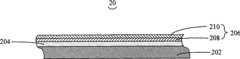
请参阅图2,本发明实施例提供的另一种导电胶带20,该导电胶带20与第一实施例的导电胶带10不同之处在于,本实施例中,导电胶带20的碳纳米管薄膜结构层206为双层结构,在该双层碳纳米管薄膜结构层206中,两层碳纳米管薄膜208、210的定向排列方向为相互垂直。通过实验测量,测得本实施例的相互垂直的双层碳纳米管薄膜导电胶带20沿着较靠近胶粘层204的第一层碳纳米管薄膜208拉伸方向的电阻为1.7KΩ/cm,沿着较远离胶粘层204的第二层碳纳米管薄膜210拉伸方向的电阻为1.3KΩ/cm。由此可见,双层碳纳米管薄膜结构层206相比于单层碳纳米管薄膜,不但电阻降低,而且不同方向的导电性也更加趋于一致。Please refer to Fig. 2, another kind of conductive adhesive tape 20 that the embodiment of the present invention provides, the difference between this conductive adhesive tape 20 and the conductive
当然,该两层碳纳米管薄膜206、208的定向排列的方向可以相交为任意角度。碳纳米管薄膜的层数也可为两层以上,各层间的碳纳米管薄膜的定向排列方向也可相交为任意角度。由于碳纳米管沿轴向方向的导电性最佳,因此,多层碳纳米管薄膜的定向排列方向相交为任意角度,可使该导电胶带的导电性趋向于各向同性,可以有效减少导电胶带纵向电阻和横向电阻的差距。另外,还可通过控制碳纳米管薄膜层的层数,在一定范围内调节导电胶带的电阻。Of course, the directions of alignment of the two
需要指出的是,在实际使用中,人们不但要求导电胶带在其平面内具有良好导电性,同时还需要在导电胶带的厚度方向上也导通。因此,可以通过折叠胶带的方法来实现。将图2所示导电胶带20的背面对折粘结之后,不但使得导电胶带双面导电,而且在厚度方向也具有良好的导电性。It should be pointed out that in actual use, people not only require the conductive tape to have good conductivity in its plane, but also need to be conductive in the thickness direction of the conductive tape. Therefore, it can be achieved by the method of folding the tape. After the back of the conductive tape 20 shown in FIG. 2 is folded and bonded, not only the conductive tape is conductive on both sides, but also has good conductivity in the thickness direction.
请参阅图3,本发明实施提供一种导电胶带的制造方法,该制造方法包括以下步骤:Please refer to Fig. 3, the implementation of the present invention provides a kind of manufacturing method of conductive adhesive tape, and this manufacturing method comprises the following steps:
(100a)制备碳纳米管薄膜结构层及胶粘剂;(100a) preparing a carbon nanotube film structure layer and an adhesive;
(200a)将胶粘剂均匀涂覆在基层上并干燥基层上的胶粘剂以形成胶粘层;及(200a) uniformly coating the adhesive on the base layer and drying the adhesive on the base layer to form an adhesive layer; and
(300a)将碳纳米管薄膜结构层压在固定好的胶粘层上使该胶粘层位于该碳纳米管薄膜结构层与该基层之间。(300a) Laminating the carbon nanotube thin film structure on the fixed adhesive layer so that the adhesive layer is located between the carbon nanotube thin film structure layer and the base layer.
在步骤(100a)中,制备碳纳米管薄膜结构层的方法包括以下步骤:(1a)提供碳纳米管阵列;及(2a)采用拉伸工具从碳纳米管阵列中拉取获得至少一层碳纳米管薄膜。In step (100a), the method for preparing a carbon nanotube thin film structure layer includes the following steps: (1a) providing a carbon nanotube array; and (2a) pulling from the carbon nanotube array using a stretching tool to obtain at least one layer of carbon nanotube film.
在步骤(1a)中,优选地,该阵列为超顺排碳纳米管阵列。本实施例中,超顺排碳纳米管阵列的制备方法采用化学气相沉积法,其具体步骤包括:(1b)提供一平整基底,本实施例优选为采用4英寸的硅基底;(2b)在基底表面均匀形成一催化剂层,该催化剂层材料可选用铁(Fe)、钴(Co)、镍(Ni)或其任意组合的合金之一;(3b)将上述形成有催化剂层的基底在700~900℃的空气中退火约30分钟~90分钟;(4b)将处理过的基底置于反应炉中,在保护气体环境下加热到500~740℃,然后通入碳源气体反应约5~30分钟,生长得到超顺排碳纳米管阵列,其高度为200~400微米。In step (1a), preferably, the array is a superparallel array of carbon nanotubes. In this embodiment, the preparation method of the super-parallel carbon nanotube array adopts the chemical vapor deposition method, and the specific steps include: (1b) providing a flat substrate, which is preferably a 4-inch silicon substrate in this embodiment; (2b) A catalyst layer is uniformly formed on the surface of the substrate, and the catalyst layer material can be selected from one of iron (Fe), cobalt (Co), nickel (Ni) or any combination thereof; Annealing in air at ~900°C for about 30 minutes to 90 minutes; (4b) Put the treated substrate in a reaction furnace, heat it to 500~740°C in a protective gas environment, and then pass through carbon source gas to react for about 5~ After 30 minutes, a super-parallel array of carbon nanotubes is grown, with a height of 200-400 microns.
该超顺排碳纳米管阵列为多个彼此平行且垂直于基底生长的碳纳米管形成的纯碳纳米管阵列。通过上述控制生长条件,该超顺排碳纳米管阵列中基本不含有杂质,如无定型碳或残留的催化剂金属颗粒等。该碳纳米管阵列中的碳纳米管彼此通过范德华力紧密接触形成阵列。上述的碳源气可选用乙炔等化学性质较活泼的碳氢化合物,保护气体可选用氮气、氨气或惰性气体。The super-parallel carbon nanotube array is a pure carbon nanotube array formed by a plurality of carbon nanotubes growing parallel to each other and perpendicular to the substrate. By controlling the growth conditions above, the super-aligned carbon nanotube array basically does not contain impurities, such as amorphous carbon or residual catalyst metal particles. The carbon nanotubes in the carbon nanotube array are in close contact with each other through van der Waals force to form an array. The above-mentioned carbon source gas can be selected from acetylene and other chemically active hydrocarbons, and the protective gas can be selected from nitrogen, ammonia or inert gas.
在步骤(2a)中,拉取碳纳米管薄膜的方法具体包括以下步骤:(1c)从上述碳纳米管阵列中选定一定宽度的多个碳纳米管片断,本实施例优选为采用具有一定宽度的胶带接触碳纳米管阵列以选定一定宽度的多个碳纳米管片断;(2c)以一定速度沿基本垂直于碳纳米管阵列生长方向拉伸该多个碳纳米管片断,以形成一连续的一层碳纳米管薄膜。In step (2a), the method for pulling the carbon nanotube film specifically includes the following steps: (1c) selecting a plurality of carbon nanotube segments with a certain width from the above-mentioned carbon nanotube array. a width of tape contacting the carbon nanotube array to select a plurality of carbon nanotube segments of a certain width; (2c) stretching the plurality of carbon nanotube segments at a certain speed along a direction substantially perpendicular to the growth direction of the carbon nanotube array to form a A continuous layer of carbon nanotube film.
在上述拉伸过程中,该多个碳纳米管片断在拉力作用下沿拉伸方向逐渐脱离基底的同时,由于范德华力作用,该选定的多个碳纳米管片断分别与其他碳纳米管片断首尾相连地连续地被拉出,从而形成一层碳纳米管薄膜。该碳纳米管薄膜为定向排列的多个碳纳米管束首尾相连形成的具有一定宽度的碳纳米管薄膜。该碳纳米管薄膜中碳纳米管的排列方向基本平行于碳纳米管薄膜的拉伸方向。During the above-mentioned stretching process, while the multiple carbon nanotube segments are gradually detached from the substrate along the stretching direction under the action of tension, due to the van der Waals force, the selected multiple carbon nanotube segments are separated from other carbon nanotube segments respectively. It is pulled out continuously end to end, thus forming a layer of carbon nanotube film. The carbon nanotube film is a carbon nanotube film with a certain width formed by connecting a plurality of aligned carbon nanotube bundles end to end. The arrangement direction of the carbon nanotubes in the carbon nanotube film is substantially parallel to the stretching direction of the carbon nanotube film.
本实施例中采用4英寸的基底生长超顺排碳纳米管阵列,该层碳纳米管薄膜的宽度可为1cm~10cm,厚度为0.01微米~100微米。当然,可根据实际情况对碳纳米管薄膜的宽度和厚度进行选择。In this embodiment, a 4-inch substrate is used to grow a super-aligned carbon nanotube array, and the carbon nanotube film may have a width of 1 cm to 10 cm and a thickness of 0.01 micron to 100 micron. Of course, the width and thickness of the carbon nanotube film can be selected according to actual conditions.
通过重复上述拉取方法,可得到多层碳纳米管薄膜,也可将拉取一层较长的碳纳米管薄膜进行剪裁而得到多层较短的碳纳米管薄膜。By repeating the pulling method above, a multilayer carbon nanotube film can be obtained, and a layer of longer carbon nanotube film can also be pulled out and cut to obtain a multilayer shorter carbon nanotube film.
另外,制备胶粘剂的方法包括:将丙烯酸丁酯、丙烯酸-2-乙基己酯、醋酸乙烯、甲基丙烯酸缩水甘油酯、丙烯酸、过氧化苯甲酰、甲苯及醋酸乙酯混合均匀分散后得到该胶粘剂。上述各种物质的质量份数分别为:112.5份的丙烯酸丁酯、116.5份的丙烯酸-2-乙基己酯、12.5份的醋酸乙烯、1.25份的甲基丙烯酸缩水甘油酯、7.5份的丙烯酸、0.5份的过氧化苯甲酰、87.5份的甲苯及162.5份的醋酸乙酯。该胶粘剂具有较高的内聚力和胶接强度,适用于制备胶粘带、自粘标签及双面胶带等。当该胶粘剂用于双面胶带时,其胶接强度可达5.6N/cm。当然,上述各种物质的质量份数可依实际需要而作相应变更,不必以本实施例为限。In addition, the method for preparing the adhesive includes: uniformly dispersing butyl acrylate, 2-ethylhexyl acrylate, vinyl acetate, glycidyl methacrylate, acrylic acid, benzoyl peroxide, toluene and ethyl acetate to obtain The adhesive. The mass parts of the above-mentioned various substances are respectively: 112.5 parts of butyl acrylate, 116.5 parts of 2-ethylhexyl acrylate, 12.5 parts of vinyl acetate, 1.25 parts of glycidyl methacrylate, 7.5 parts of acrylic acid , 0.5 parts of benzoyl peroxide, 87.5 parts of toluene and 162.5 parts of ethyl acetate. The adhesive has high cohesion and bonding strength, and is suitable for preparing adhesive tapes, self-adhesive labels and double-sided tapes. When the adhesive is used for double-sided tape, its bonding strength can reach 5.6N/cm. Certainly, the mass fractions of the above-mentioned various substances can be changed accordingly according to actual needs, and are not limited to this embodiment.
在步骤(200a)中,将制作好的胶粘剂均匀涂覆在基层上并干燥基层上的胶粘剂以形成胶粘层。干燥的方法可采用风干、热干或两者相结合。In step (200a), the prepared adhesive is evenly coated on the base layer and the adhesive on the base layer is dried to form an adhesive layer. The drying method can be air drying, heat drying or a combination of both.
在步骤(300a)中,先将带有胶粘层的基层绷紧平放于平台上并使胶粘层朝上,然后使用滚子如塑料圆棒一边滚动一边将一层碳纳米管薄膜结构层压在胶粘层上,优选地,该碳纳米管薄膜结构层的定向排列方向与导电胶带的纵向方向一致。In step (300a), the base layer with the adhesive layer is placed flat on the platform with the adhesive layer facing up, and then a layer of carbon nanotube film structure is rolled while rolling with a roller such as a plastic round rod. Laminated on the adhesive layer, preferably, the alignment direction of the carbon nanotube film structure layer is consistent with the longitudinal direction of the conductive tape.
当然,若需要制作含有两层或以上碳纳米管薄膜结构层的导电胶带,只需将第二层碳纳米管薄膜压在第一层碳纳米管薄膜之上便可,而第二层碳纳米管薄膜的定向排列方向与第一层碳纳米管薄膜的定向排列方向相交叉的角度可视实际需求而定。Of course, if you need to make a conductive tape containing two or more carbon nanotube film structural layers, you only need to press the second layer of carbon nanotube film on the first layer of carbon nanotube film, and the second layer of carbon nanotube film The angle at which the alignment direction of the tube film intersects with the alignment direction of the first layer of carbon nanotube film can be determined according to actual requirements.
本发明实施例所提供的导电胶带10、20,其碳纳米管薄膜结构层106、206形成于胶粘层104、204之上,且沿碳纳米管薄膜结构层106、206的定向排列方向的导电性佳,从而可制成任意导电方向的导电胶带10、20,该导电胶带10、20的导电性要优于使用无定形碳的导电胶带,故含碳纳米管薄膜结构层的导电胶带10、20的电阻低;制备导电胶带10、20时,如要达到同样的导电性,那么碳纳米管薄膜结构层106、206的用量会更少,因此导电胶带10、20的成本低。In the conductive
需要指出的是,本发明实施例提供的导电胶带10、20还可用于防静电包装材料,如液晶面板包装盒。It should be pointed out that the
另外,本领域技术人员还可以在本发明精神内做其它变化。当然,这些依据本发明精神所做的变化,都应包含在本发明所要求保护的范围之内。In addition, those skilled in the art can also make other changes within the spirit of the present invention. Of course, these changes made according to the spirit of the present invention should all be included within the scope of protection claimed by the present invention.
Claims (7)
Priority Applications (2)
| Application Number | Priority Date | Filing Date | Title |
|---|---|---|---|
| CN200710073979.5ACN101280161B (en) | 2007-04-06 | 2007-04-06 | Conducting adhesive tape and manufacturing method thereof |
| US11/967,115US7854992B2 (en) | 2007-04-06 | 2007-12-29 | Conductive tape and method for making the same |
Applications Claiming Priority (1)
| Application Number | Priority Date | Filing Date | Title |
|---|---|---|---|
| CN200710073979.5ACN101280161B (en) | 2007-04-06 | 2007-04-06 | Conducting adhesive tape and manufacturing method thereof |
Publications (2)
| Publication Number | Publication Date |
|---|---|
| CN101280161A CN101280161A (en) | 2008-10-08 |
| CN101280161Btrue CN101280161B (en) | 2013-01-09 |
Family
ID=39825956
Family Applications (1)
| Application Number | Title | Priority Date | Filing Date |
|---|---|---|---|
| CN200710073979.5AActiveCN101280161B (en) | 2007-04-06 | 2007-04-06 | Conducting adhesive tape and manufacturing method thereof |
Country Status (2)
| Country | Link |
|---|---|
| US (1) | US7854992B2 (en) |
| CN (1) | CN101280161B (en) |
Cited By (2)
| Publication number | Priority date | Publication date | Assignee | Title |
|---|---|---|---|---|
| CN104194664A (en)* | 2014-08-22 | 2014-12-10 | 桐城信邦电子有限公司 | Conductive tape |
| TWI694127B (en) | 2017-12-28 | 2020-05-21 | 鴻海精密工業股份有限公司 | A bonding method |
Families Citing this family (51)
| Publication number | Priority date | Publication date | Assignee | Title |
|---|---|---|---|---|
| CN101409962B (en)* | 2007-10-10 | 2010-11-10 | 清华大学 | Surface heat light source and preparation method thereof |
| CN101400198B (en) | 2007-09-28 | 2010-09-29 | 北京富纳特创新科技有限公司 | Surface heating light source, preparation thereof and method for heat object application |
| CN101458599B (en) | 2007-12-14 | 2011-06-08 | 清华大学 | Touch screen, method for producing the touch screen, and display device using the touch screen |
| CN101464763B (en) | 2007-12-21 | 2010-09-29 | 清华大学 | Manufacturing method of touch screen |
| CN101458594B (en) | 2007-12-12 | 2012-07-18 | 清华大学 | Touch screen and display device |
| CN101458602B (en)* | 2007-12-12 | 2011-12-21 | 清华大学 | Touch screen and display device |
| CN101458603B (en) | 2007-12-12 | 2011-06-08 | 北京富纳特创新科技有限公司 | Touch screen and display device |
| CN101458600B (en) | 2007-12-14 | 2011-11-30 | 清华大学 | Touch screen and display device |
| CN101458604B (en) | 2007-12-12 | 2012-03-28 | 清华大学 | Touch screen and display device |
| CN101458595B (en) | 2007-12-12 | 2011-06-08 | 清华大学 | Touch screen and display device |
| CN101470560B (en)* | 2007-12-27 | 2012-01-25 | 清华大学 | Touch screen and display equipment |
| CN101458598B (en) | 2007-12-14 | 2011-06-08 | 清华大学 | Touch screen and display device |
| CN101656769B (en) | 2008-08-22 | 2012-10-10 | 清华大学 | Mobile telephone |
| CN101458608B (en) | 2007-12-14 | 2011-09-28 | 清华大学 | Touch screen preparation method |
| CN101458593B (en) | 2007-12-12 | 2012-03-14 | 清华大学 | Touch screen and display device |
| CN101458596B (en)* | 2007-12-12 | 2011-06-08 | 北京富纳特创新科技有限公司 | Touch screen and display device |
| CN101458606B (en)* | 2007-12-12 | 2012-06-20 | 清华大学 | Touch screen, method for producing the touch screen, and display device using the touch screen |
| CN101419518B (en) | 2007-10-23 | 2012-06-20 | 清华大学 | Touch panel |
| CN101655720B (en) | 2008-08-22 | 2012-07-18 | 清华大学 | Personal digital assistant |
| CN101470559B (en)* | 2007-12-27 | 2012-11-21 | 清华大学 | Touch screen and display equipment |
| CN101419519B (en)* | 2007-10-23 | 2012-06-20 | 清华大学 | Touch panel |
| CN101458609B (en) | 2007-12-14 | 2011-11-09 | 清华大学 | Touch screen and display device |
| CN101470566B (en)* | 2007-12-27 | 2011-06-08 | 清华大学 | Touch control device |
| CN101470558B (en) | 2007-12-27 | 2012-11-21 | 清华大学 | Touch screen and display equipment |
| CN101458605B (en)* | 2007-12-12 | 2011-03-30 | 鸿富锦精密工业(深圳)有限公司 | Touch screen and display device |
| CN101458597B (en) | 2007-12-14 | 2011-06-08 | 清华大学 | Touch screen, method for producing the touch screen, and display device using the touch screen |
| CN101458975B (en) | 2007-12-12 | 2012-05-16 | 清华大学 | Electronic element |
| CN101464757A (en)* | 2007-12-21 | 2009-06-24 | 清华大学 | Touch screen and display equipment |
| CN101458601B (en)* | 2007-12-14 | 2012-03-14 | 清华大学 | Touch screen and display device |
| CN101458607B (en) | 2007-12-14 | 2010-12-29 | 清华大学 | Touch screen and display device |
| CN101464766B (en)* | 2007-12-21 | 2011-11-30 | 清华大学 | Touch screen and display equipment |
| CN101470565B (en) | 2007-12-27 | 2011-08-24 | 清华大学 | Touch screen and display device |
| CN101464765B (en) | 2007-12-21 | 2011-01-05 | 鸿富锦精密工业(深圳)有限公司 | Touch screen and display equipment |
| US8574393B2 (en) | 2007-12-21 | 2013-11-05 | Tsinghua University | Method for making touch panel |
| CN101464764B (en) | 2007-12-21 | 2012-07-18 | 清华大学 | Touch screen and display equipment |
| US7881785B2 (en)* | 2008-03-26 | 2011-02-01 | Cardiac Science Corporation | Method and apparatus for defrosting a defibrillation electrode |
| US8237677B2 (en) | 2008-07-04 | 2012-08-07 | Tsinghua University | Liquid crystal display screen |
| US8390580B2 (en) | 2008-07-09 | 2013-03-05 | Tsinghua University | Touch panel, liquid crystal display screen using the same, and methods for making the touch panel and the liquid crystal display screen |
| US20110262772A1 (en)* | 2008-07-31 | 2011-10-27 | William Marsh Rice University | Method for Producing Aligned Near Full Density Pure Carbon Nanotube Sheets, Ribbons, and Films From Aligned Arrays of as Grown Carbon Nanotube Carpets/Forests and Direct Transfer to Metal and Polymer Surfaces |
| CN101920955B (en) | 2009-06-09 | 2012-09-19 | 清华大学 | Carbon nanotube film protective structure and preparation method thereof |
| CN101924816B (en)* | 2009-06-12 | 2013-03-20 | 清华大学 | Flexible mobile phone |
| CN101944403A (en)* | 2009-07-08 | 2011-01-12 | 群康科技(深圳)有限公司 | Electric-conducting plate and manufacturing method thereof |
| CN101989469A (en)* | 2009-07-31 | 2011-03-23 | 群康科技(深圳)有限公司 | Current-conducting plate |
| CN101880035A (en) | 2010-06-29 | 2010-11-10 | 清华大学 | carbon nanotube structure |
| US10029834B2 (en) | 2013-10-15 | 2018-07-24 | Thomas & Betts International Llc | Cable tie employing composite of nylon and carbon nanotubes |
| CN104559826B (en)* | 2014-12-30 | 2017-03-15 | 桐城信邦电子有限公司 | A kind of conductive tape |
| CN107249880B (en)* | 2015-02-23 | 2020-08-04 | 琳得科美国股份有限公司 | Adhesive sheet |
| JP6704229B2 (en) | 2015-09-14 | 2020-06-03 | リンテック オブ アメリカ インコーポレーテッドLintec of America, Inc. | Flexible sheet, heat conductive member, conductive member, antistatic member, heating element, electromagnetic wave shield, and method for manufacturing flexible sheet |
| CN109971387B (en)* | 2017-12-28 | 2021-01-22 | 清华大学 | Application of carbon nanotube structure as double-sided adhesive tape |
| KR102693822B1 (en)* | 2018-09-03 | 2024-08-12 | 삼성전자 주식회사 | In and out port and electronic device including the same |
| CN116327202B (en)* | 2022-11-29 | 2025-04-18 | 大连大学附属中山医院 | Application of a flexible electrode in wearable devices |
Citations (1)
| Publication number | Priority date | Publication date | Assignee | Title |
|---|---|---|---|---|
| CN1483667A (en)* | 2002-09-16 | 2004-03-24 | �廪��ѧ | A carbon nanotube rope and its manufacturing method |
Family Cites Families (4)
| Publication number | Priority date | Publication date | Assignee | Title |
|---|---|---|---|---|
| US4308912A (en)* | 1979-03-28 | 1982-01-05 | Knecht Bernath L | Heat transfer system |
| WO1999065821A1 (en)* | 1998-06-19 | 1999-12-23 | The Research Foundation Of State University Of New York | Free-standing and aligned carbon nanotubes and synthesis thereof |
| JP2005097003A (en)* | 2000-05-31 | 2005-04-14 | Nec Corp | Method for fixing carbon nanotube |
| CN1296994C (en)* | 2002-11-14 | 2007-01-24 | 清华大学 | A thermal interfacial material and method for manufacturing same |
- 2007
- 2007-04-06CNCN200710073979.5Apatent/CN101280161B/enactiveActive
- 2007-12-29USUS11/967,115patent/US7854992B2/enactiveActive
Patent Citations (1)
| Publication number | Priority date | Publication date | Assignee | Title |
|---|---|---|---|---|
| CN1483667A (en)* | 2002-09-16 | 2004-03-24 | �廪��ѧ | A carbon nanotube rope and its manufacturing method |
Cited By (2)
| Publication number | Priority date | Publication date | Assignee | Title |
|---|---|---|---|---|
| CN104194664A (en)* | 2014-08-22 | 2014-12-10 | 桐城信邦电子有限公司 | Conductive tape |
| TWI694127B (en) | 2017-12-28 | 2020-05-21 | 鴻海精密工業股份有限公司 | A bonding method |
Also Published As
| Publication number | Publication date |
|---|---|
| US20080245548A1 (en) | 2008-10-09 |
| US7854992B2 (en) | 2010-12-21 |
| CN101280161A (en) | 2008-10-08 |
Similar Documents
| Publication | Publication Date | Title |
|---|---|---|
| CN101280161B (en) | Conducting adhesive tape and manufacturing method thereof | |
| JP6788013B2 (en) | Multi-layer composite with adhesive and one or more nanofiber sheets | |
| US8906191B2 (en) | Method for making protective device for protecting carbon nanotube film | |
| US20170038860A1 (en) | Touch panel | |
| TWI824186B (en) | Sheet, heating element and heating device | |
| CN101734645B (en) | carbon nano-tube film | |
| US8920661B2 (en) | Method for making graphene/carbon nanotube composite structure | |
| US8597526B2 (en) | Method for making graphene/carbon nanotube composite structure | |
| US8025971B2 (en) | Fibrous columnar structure aggregate and pressure-sensitive adhesive member using the aggregate | |
| CN102159499B (en) | aggregates of carbon nanotubes | |
| CN101734644B (en) | Method for stretching carbon nano-tube films | |
| Yim et al. | Fabrication of transparent single wall carbon nanotube films with low sheet resistance | |
| US8318033B2 (en) | Conductive tape and method for making the same | |
| CN101239712A (en) | Carbon nanotube film structure and preparation method thereof | |
| US20120104213A1 (en) | Carbon nanotube film supporting structure and method for using same | |
| CN102061101A (en) | Carbon nano tube composite material | |
| CN101870465A (en) | Preparation method of carbon nano tube film | |
| US8852376B2 (en) | Method for making heaters | |
| CN101290857A (en) | Field emission cathode and its preparation method | |
| CN107709232A (en) | CNT woods layered product and the method for producing CNT woods layered product | |
| TW201020209A (en) | Carbon nanotube film | |
| TWI344981B (en) | Conductive tape and method for making the same | |
| CN109436916B (en) | Continuous collection method and device for carbon nanotube film | |
| TWI462838B (en) | Carbon nanotube film protecting structure and method for making the same | |
| CN102207574A (en) | Polarization element and manufacturing method thereof |
Legal Events
| Date | Code | Title | Description |
|---|---|---|---|
| C06 | Publication | ||
| PB01 | Publication | ||
| C10 | Entry into substantive examination | ||
| SE01 | Entry into force of request for substantive examination | ||
| C14 | Grant of patent or utility model | ||
| GR01 | Patent grant |