CN101278404B - Transistor element, display device and their manufacturing method - Google Patents
Transistor element, display device and their manufacturing methodDownload PDFInfo
- Publication number
- CN101278404B CN101278404BCN2006800368229ACN200680036822ACN101278404BCN 101278404 BCN101278404 BCN 101278404BCN 2006800368229 ACN2006800368229 ACN 2006800368229ACN 200680036822 ACN200680036822 ACN 200680036822ACN 101278404 BCN101278404 BCN 101278404B
- Authority
- CN
- China
- Prior art keywords
- transistor
- interlayer dielectric
- insulating film
- organic
- interlayer insulating
- Prior art date
- Legal status (The legal status is an assumption and is not a legal conclusion. Google has not performed a legal analysis and makes no representation as to the accuracy of the status listed.)
- Expired - Fee Related
Links
Images


Classifications
- H—ELECTRICITY
- H10—SEMICONDUCTOR DEVICES; ELECTRIC SOLID-STATE DEVICES NOT OTHERWISE PROVIDED FOR
- H10K—ORGANIC ELECTRIC SOLID-STATE DEVICES
- H10K19/00—Integrated devices, or assemblies of multiple devices, comprising at least one organic element specially adapted for rectifying, amplifying, oscillating or switching, covered by group H10K10/00
- H10K19/10—Integrated devices, or assemblies of multiple devices, comprising at least one organic element specially adapted for rectifying, amplifying, oscillating or switching, covered by group H10K10/00 comprising field-effect transistors
- H—ELECTRICITY
- H10—SEMICONDUCTOR DEVICES; ELECTRIC SOLID-STATE DEVICES NOT OTHERWISE PROVIDED FOR
- H10K—ORGANIC ELECTRIC SOLID-STATE DEVICES
- H10K10/00—Organic devices specially adapted for rectifying, amplifying, oscillating or switching; Organic capacitors or resistors having potential barriers
- H10K10/40—Organic transistors
- H10K10/46—Field-effect transistors, e.g. organic thin-film transistors [OTFT]
- H10K10/462—Insulated gate field-effect transistors [IGFETs]
- H10K10/468—Insulated gate field-effect transistors [IGFETs] characterised by the gate dielectrics
- H10K10/478—Insulated gate field-effect transistors [IGFETs] characterised by the gate dielectrics the gate dielectric comprising a layer of composite material comprising interpenetrating or embedded materials, e.g. TiO2 particles in a polymer matrix
- G—PHYSICS
- G02—OPTICS
- G02F—OPTICAL DEVICES OR ARRANGEMENTS FOR THE CONTROL OF LIGHT BY MODIFICATION OF THE OPTICAL PROPERTIES OF THE MEDIA OF THE ELEMENTS INVOLVED THEREIN; NON-LINEAR OPTICS; FREQUENCY-CHANGING OF LIGHT; OPTICAL LOGIC ELEMENTS; OPTICAL ANALOGUE/DIGITAL CONVERTERS
- G02F1/00—Devices or arrangements for the control of the intensity, colour, phase, polarisation or direction of light arriving from an independent light source, e.g. switching, gating or modulating; Non-linear optics
- G02F1/01—Devices or arrangements for the control of the intensity, colour, phase, polarisation or direction of light arriving from an independent light source, e.g. switching, gating or modulating; Non-linear optics for the control of the intensity, phase, polarisation or colour
- G02F1/13—Devices or arrangements for the control of the intensity, colour, phase, polarisation or direction of light arriving from an independent light source, e.g. switching, gating or modulating; Non-linear optics for the control of the intensity, phase, polarisation or colour based on liquid crystals, e.g. single liquid crystal display cells
- G02F1/133—Constructional arrangements; Operation of liquid crystal cells; Circuit arrangements
- G02F1/136—Liquid crystal cells structurally associated with a semi-conducting layer or substrate, e.g. cells forming part of an integrated circuit
- H—ELECTRICITY
- H10—SEMICONDUCTOR DEVICES; ELECTRIC SOLID-STATE DEVICES NOT OTHERWISE PROVIDED FOR
- H10K—ORGANIC ELECTRIC SOLID-STATE DEVICES
- H10K10/00—Organic devices specially adapted for rectifying, amplifying, oscillating or switching; Organic capacitors or resistors having potential barriers
- H—ELECTRICITY
- H10—SEMICONDUCTOR DEVICES; ELECTRIC SOLID-STATE DEVICES NOT OTHERWISE PROVIDED FOR
- H10K—ORGANIC ELECTRIC SOLID-STATE DEVICES
- H10K85/00—Organic materials used in the body or electrodes of devices covered by this subclass
- H10K85/10—Organic polymers or oligomers
- H10K85/111—Organic polymers or oligomers comprising aromatic, heteroaromatic, or aryl chains, e.g. polyaniline, polyphenylene or polyphenylene vinylene
Landscapes
- Chemical & Material Sciences (AREA)
- Engineering & Computer Science (AREA)
- Materials Engineering (AREA)
- Physics & Mathematics (AREA)
- Composite Materials (AREA)
- Nonlinear Science (AREA)
- Crystallography & Structural Chemistry (AREA)
- General Physics & Mathematics (AREA)
- Optics & Photonics (AREA)
- Mathematical Physics (AREA)
- Microelectronics & Electronic Packaging (AREA)
- Thin Film Transistor (AREA)
- Electroluminescent Light Sources (AREA)
Abstract
Description
Translated fromChinese技术领域technical field
本发明总体上涉及晶体管元件。尤其,本发明涉及用于稳定驱动晶体管元件的元件结构,该晶体管元件具有经由层间绝缘膜连接至有机半导体的上部电极。The present invention generally relates to transistor elements. In particular, the present invention relates to an element structure for stably driving a transistor element having an upper electrode connected to an organic semiconductor via an interlayer insulating film.
背景技术Background technique
代替用于常规晶体管的无机材料如硅单晶和非晶硅,近来已经进行了使用有机半导体材料的晶体管的开发。与使用无机材料的情况相比,由于其制造方法简单容易并且有可能在低温下大面积成层,因此使用有机半导体的晶体管具有低成本的优点。由于有机材料的柔性,有可能形成柔性塑料基板,因此对于使用有机半导体的晶体管而言,已期待其应用开发,例如包括显示装置在内的各种电子装置的驱动元件。Instead of inorganic materials such as silicon single crystal and amorphous silicon used for conventional transistors, development of transistors using organic semiconductor materials has recently been conducted. Transistors using organic semiconductors have an advantage of low cost compared to the case of using inorganic materials because of the simplicity and ease of their manufacturing method and the possibility of layering a large area at low temperature. Due to the flexibility of organic materials, it is possible to form flexible plastic substrates, so for transistors using organic semiconductors, their application development has been expected, such as driving elements of various electronic devices including display devices.
在将使用排列成二维阵列的有机半导体层的晶体管用作驱动显示装置等的有源矩阵基板的情况中,例如,需要形成设置有经由层间绝缘膜与所述有机半导体层电连通的上部电极的结构。作为层间绝缘膜,通常,使用利用溅射法和CVD(化学气相沉积)形成如氧化硅和氮化硅的无机材料的方法。然而,问题在于在这些真空工艺中有许多步骤并且由于形成通孔而使晶体管的特性劣化。In the case of using a transistor using an organic semiconductor layer arranged in a two-dimensional array as an active matrix substrate for driving a display device or the like, for example, it is necessary to form an upper portion provided with an upper portion electrically connected to the organic semiconductor layer via an interlayer insulating film. Electrode structure. As an interlayer insulating film, generally, a method of forming an inorganic material such as silicon oxide and silicon nitride using a sputtering method and CVD (Chemical Vapor Deposition) is used. However, there are problems in that there are many steps in these vacuum processes and the characteristics of transistors are degraded due to the formation of via holes.
而且,对于具有图1所示结构的晶体管元件,由于设置层间绝缘膜作为栅极绝缘膜并且因上部电极设置在有机半导体的相对侧将所述层间绝缘膜夹在中间而在所述有机半导体层中形成不必要的通道,因此存在断开电流(OFF-current)增大的问题。例如,报道了在使用有机晶体管的柔性基板上制造QVGA电泳显示装置的结果(参见非专利文献1)。在栅电压为正电压的情况中,通过从正到负改变像素电极(pixel electrode)的电流电势使断开电流增大。在非专利文献1中公开:即使构成晶体管元件的层间绝缘膜的电容约为栅极绝缘膜的1/20,由于像素电极的影响,仍在有机半导体中产生第二通道,然而未提及其解决方法。Furthermore, for the transistor element having the structure shown in FIG. 1, since an interlayer insulating film is provided as a gate insulating film and since an upper electrode is provided on opposite sides of an organic semiconductor to sandwich the interlayer insulating film Since unnecessary channels are formed in the semiconductor layer, there is a problem that off-current (OFF-current) increases. For example, the results of manufacturing a QVGA electrophoretic display device on a flexible substrate using organic transistors are reported (see Non-Patent Document 1). In case the gate voltage is a positive voltage, the off current is increased by changing the current potential of the pixel electrode from positive to negative. It is disclosed in Non-Patent Document 1 that even if the capacitance of the interlayer insulating film constituting the transistor element is about 1/20 of that of the gate insulating film, due to the influence of the pixel electrode, a second channel is still generated in the organic semiconductor, but it is not mentioned its workaround.
另一方面,公开了许多以上所示结构的有机晶体管元件,但是多数与栅极绝缘膜的改进有关。其中,关于在有源层的无栅极绝缘膜的一侧设置的绝缘膜(层间绝缘膜),例如,使用包括芳族化合物和/或芳环成分聚合物的材料作为层间绝缘膜。通过这样,实现了溶液处理的低成本化并且公开了可以改进有机晶体管迁移率的有机场效应晶体管(例如,参见专利文献1)。然而,没有关于形成通孔和上部电极的描述,因此它没有解决上面的问题。On the other hand, many organic transistor elements having the structures shown above are disclosed, but most of them relate to the improvement of the gate insulating film. Here, regarding the insulating film (interlayer insulating film) provided on the side of the active layer without the gate insulating film, for example, a material including an aromatic compound and/or an aromatic ring component polymer is used as the interlayer insulating film. Through this, cost reduction of solution processing is achieved and an organic field effect transistor that can improve the mobility of an organic transistor is disclosed (for example, see Patent Document 1). However, there is no description about forming via holes and upper electrodes, so it does not solve the above problems.
公开了在层间绝缘膜和半导体膜的界面上提供5nm以上且不大于40nm的不均匀度来提供其中漏电流得以抑制且工作稳定的晶体管的技术(例如,参见专利文献2)。对于形成包含无机材料的层间绝缘膜,该技术通过使用氢等离子体制造不均匀度;于是,形成多晶硅有源层。A technique of providing a nonuniformity of 5 nm or more and not more than 40 nm on the interface of an interlayer insulating film and a semiconductor film to provide a transistor in which leakage current is suppressed and operates stably is disclosed (for example, see Patent Document 2). For forming an interlayer insulating film containing an inorganic material, this technique produces unevenness by using hydrogen plasma; thus, a polysilicon active layer is formed.
还公开了提供有机薄膜晶体管的技术,在该有机薄膜晶体管中通过双栅极结构控制更多的电流并可使其流走,该双栅极结构在包含有机半导体层的有源层之上和之下具有一对栅极绝缘膜和栅电极。(例如,参见专利文献3)在该结构的晶体管中,通过施加与上部栅电极和下部栅电极同步的控制电压,能够运送更多的电流,使得分别在有源层中的上下栅电极附近形成通道。该技术利用了在有源层中形成多通道的事实;另一方面,当无法充分控制双栅极结构的晶体管中的各栅电压时,其暗示会如非专利文献1中所述形成不必要的通道。Also disclosed are techniques for providing organic thin film transistors in which more current is controlled and can flow away through a double gate structure over an active layer comprising an organic semiconductor layer and There is a pair of gate insulating film and gate electrode underneath. (For example, see Patent Document 3) In the transistor of this structure, by applying a control voltage synchronized with the upper gate electrode and the lower gate electrode, it is possible to carry more current, so that the active layer is formed near the upper and lower gate electrodes, respectively. aisle. This technology utilizes the fact that multiple channels are formed in the active layer; channel.
此外,公开了薄层晶体管的结构,在该薄层晶体管中,光电器件的TFT包括上部遮光层和下部遮光层,并且通过将通道区域设置在数据线和扫描线的交叉区域中改进耐光性能和显示质量。(例如,参见专利文献4)此外,公开了半导体器件,其中该半导体器件包括依次在基板上形成的栅电极、栅极绝缘膜和源/漏电极;填充在源/漏电极之间的有机半导体;和绝缘膜,其形成为与其上的源/漏电极表面接触。(例如,参见专利文献5)In addition, a structure of a thin layer transistor is disclosed, in which a TFT of a photoelectric device includes an upper light shielding layer and a lower light shielding layer, and the light resistance performance and the Display quality. (For example, see Patent Document 4) Further, a semiconductor device is disclosed, wherein the semiconductor device includes a gate electrode, a gate insulating film, and source/drain electrodes sequentially formed on a substrate; an organic semiconductor filled between the source/drain electrodes ; and an insulating film formed in contact with the source/drain electrode surface thereon. (For example, see Patent Document 5)
专利文献1:JP 2005-101555,APatent Document 1: JP 2005-101555, A
专利文献2:JP 2004-247434,APatent Document 2: JP 2004-247434, A
专利文献3:JP 2005-079549,APatent Document 3: JP 2005-079549, A
专利文献4:JP 2004-126557,APatent Document 4: JP 2004-126557, A
专利文献5:JP 2005-223049,APatent Document 5: JP 2005-223049, A
非专利文献1:SID 05 DIGEST 3.1:Invited Paper:Rollable QVGAActive-Matrix Displays Based on Organic Electronics,G.H.Gelinck,H.E.Huitema,M.van Mil,E.van Veenendaal,P.J.G.van Lieshout and F.J.Touwslager,Polymer Vision/Philips Research Laboratories,Eindhoven,TheNetherlandsNon-Patent Document 1:
发明内容Contents of the invention
在图1所示的晶体管元件的结构中,通过将上部电极设置在与有机半导体层相对的另一侧而将所述层间绝缘膜夹在中间,由此,当施加源/漏电压时该电压将施加至所述上部电极。结果,如上所述,问题是通过使作为栅电极的上部电极和作为栅极绝缘膜的层间绝缘膜起作用,而在有机半导体层中形成不必要的通道。当在晶体管的断开状态(off-state)下在有机半导体层中形成通道时,断开电流增大导致开/关(ON/OFF)比降低并且晶体管特性劣化。因此,这变为严重的问题。作为该问题的解决方法,假设形成难以充当栅极绝缘层的层间绝缘膜。即,与要求栅极绝缘膜具有优异性能相反,认为介电常数应该低,厚度应该大,并且与有机半导体层的界面应该不平。然而,实际上,还没有方法形成具有通孔而不导致晶体管损害的满足上述条件的层间绝缘膜。In the structure of the transistor element shown in FIG. 1, the interlayer insulating film is sandwiched by disposing the upper electrode on the other side opposite to the organic semiconductor layer, whereby when a source/drain voltage is applied, the A voltage will be applied to the upper electrode. As a result, as described above, there is a problem that an unnecessary channel is formed in the organic semiconductor layer by causing the upper electrode as the gate electrode and the interlayer insulating film as the gate insulating film to function. When a channel is formed in an organic semiconductor layer in an off-state of a transistor, an increase in off-current causes ON/OFF ratio to decrease and transistor characteristics to deteriorate. Therefore, this becomes a serious problem. As a solution to this problem, it is assumed that an interlayer insulating film that is difficult to function as a gate insulating layer is formed. That is, contrary to the requirement that the gate insulating film has excellent properties, it is considered that the dielectric constant should be low, the thickness should be large, and the interface with the organic semiconductor layer should be uneven. Actually, however, there has been no method of forming an interlayer insulating film satisfying the above-mentioned conditions having a via hole without causing damage to the transistor.
本发明的总体目的是解决上述问题。即,本发明的总体目的是提供具有形成工艺不损害晶体管的层间绝缘膜且未在有机半导体中形成不必要的通道的晶体管元件。本发明更具体的目的在于提供晶体管元件,其中通过使用由有机材料和颗粒的混合物构成的层间绝缘膜而难以在有机半导体中形成不必要的通道,且制造方法简单,不使晶体管特性劣化。此外,本发明的总体目的是提供使用所述晶体管元件的显示装置和它们的制造方法。The general purpose of the present invention is to solve the above-mentioned problems. That is, a general object of the present invention is to provide a transistor element having a formation process that does not damage an interlayer insulating film of a transistor and does not form an unnecessary channel in an organic semiconductor. A more specific object of the present invention is to provide a transistor element in which it is difficult to form an unnecessary channel in an organic semiconductor by using an interlayer insulating film composed of a mixture of an organic material and particles, and the manufacturing method is simple without deteriorating transistor characteristics. Furthermore, a general object of the present invention is to provide a display device using the transistor element and their manufacturing method.
结果,对于层叠有在基板上使用有机半导体层的晶体管、接触该有机半导体层的层间绝缘膜和经由层间绝缘膜中设置的通孔与所述晶体管电接触的上部电极的元件,通过使用由有机材料和颗粒的混合物构成的层间绝缘膜,获得可实现上述目的的晶体管元件,于是完成本发明。As a result, for an element stacked with a transistor using an organic semiconductor layer on a substrate, an interlayer insulating film contacting the organic semiconductor layer, and an upper electrode electrically contacting the transistor through a via hole provided in the interlayer insulating film, by using An interlayer insulating film composed of a mixture of an organic material and particles, a transistor element capable of achieving the above object is obtained, and thus the present invention has been accomplished.
为实现上述目的,根据本发明的一个方面,提供一种晶体管元件,其层叠有:在基板上使用有机半导体层的晶体管、接触该有机半导体层的层间绝缘膜和经由层间绝缘膜中设置的通孔与所述晶体管电接触的上部电极,其中所述层间绝缘膜包括有机材料和颗粒的混合物。In order to achieve the above object, according to one aspect of the present invention, there is provided a transistor element which is laminated with: a transistor using an organic semiconductor layer on a substrate, an interlayer insulating film contacting the organic semiconductor layer, and a transistor provided via the interlayer insulating film. The via hole is in electrical contact with the upper electrode of the transistor, wherein the interlayer insulating film includes a mixture of organic material and particles.
根据本发明,对于层叠有在基板上使用有机半导体层的晶体管、接触该有机半导体层的层间绝缘膜和经由层间绝缘膜中设置的通孔与所述晶体管电接触的上部电极的元件,通过由有机材料和颗粒的混合物构成的层间绝缘膜,难以在所述有机半导体层中形成不必要的通道并且有可能获得具有优异的开/关比的晶体管元件。此外,通过将该晶体管元件与选自液晶显示元件、电泳显示元件和有机电致发光显示元件的图像显示元件结合使用,可以提供显示装置,该显示装置具有良好的性能,薄且重量轻,对人眼的负担小,并且是平板型或柔性的。According to the present invention, for an element in which a transistor using an organic semiconductor layer on a substrate, an interlayer insulating film contacting the organic semiconductor layer, and an upper electrode electrically contacting the transistor through a via hole provided in the interlayer insulating film are stacked, With the interlayer insulating film composed of a mixture of organic materials and particles, it is difficult to form unnecessary channels in the organic semiconductor layer and it is possible to obtain a transistor element having an excellent on/off ratio. In addition, by using the transistor element in combination with an image display element selected from a liquid crystal display element, an electrophoretic display element, and an organic electroluminescence display element, a display device having good performance, being thin and light in weight, can be provided. The burden on human eyes is small, and it is flat or flexible.
由以下详细描述,本发明的其它目的、特征和优点将变得更加明显。Other objects, features and advantages of the present invention will become more apparent from the following detailed description.
附图说明Description of drawings
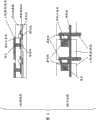
图1是显示有机晶体管元件的基本结构;Figure 1 shows the basic structure of an organic transistor device;
图2是显示无机颗粒粒径分布的图;Figure 2 is a graph showing the particle size distribution of inorganic particles;
图3是显示晶体管的Cr及其开/关比的图,在该晶体管中CI通过改变本发明晶体管元件的层间绝缘膜的膜厚度和相对介电常数而改变;Fig. 3 is a graph showing Cr and its on/off ratio of a transistor in whichC is changed by changing the film thickness and relative permittivity of the interlayer insulating film of the transistor element of the present invention;
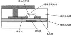
图4是显示本发明晶体管元件的结构的图,其中(A)是它的截面图而(B)是它的平面图;4 is a diagram showing the structure of the transistor element of the present invention, wherein (A) is its cross-sectional view and (B) is its plan view;
图5是显示本发明的通道形成部分的图;Fig. 5 is a diagram showing a channel forming part of the present invention;
图6是显示本发明的显示装置的图;FIG. 6 is a diagram showing a display device of the present invention;
图7是显示实施例1的晶体管性能的评价结果的图;7 is a graph showing evaluation results of transistor performance of Example 1;
图8是显示对比例1的晶体管性能的评价结果的图;和8 is a graph showing evaluation results of transistor performance of Comparative Example 1; and
图9是显示实施例2的晶体管性能的评价结果的图。FIG. 9 is a graph showing evaluation results of transistor performance in Example 2. FIG.
具体实施方式Detailed ways
接下来,参照附图,给出本发明实施方式的描述。本发明不限于具体公开的实施方式,并且可以在不背离本发明范围的情况下进行改变和更改。Next, with reference to the drawings, a description will be given of embodiments of the present invention. The present invention is not limited to the specifically disclosed embodiments, and changes and modifications may be made without departing from the scope of the invention.
本发明包括层叠了下列的晶体管元件:在基板上使用有机半导体层的晶体管、与所述有机半导体层接触的层间绝缘膜,经由在所述层间绝缘膜中设置的通孔与所述晶体管电连接的上部电极,其中所述层间绝缘膜由有机材料和颗粒的混合物构成,并且在所述有机半导体层中难以形成不必要的通道,且所述晶体管元件有可能具有优异的开/关比。The present invention includes a transistor element in which: a transistor using an organic semiconductor layer on a substrate, an interlayer insulating film in contact with the organic semiconductor layer, and the transistor through a via hole provided in the interlayer insulating film are stacked. An electrically connected upper electrode, wherein the interlayer insulating film is composed of a mixture of organic materials and particles, and it is difficult to form unnecessary channels in the organic semiconductor layer, and the transistor element is likely to have excellent on/off Compare.
首先,描述层间绝缘膜的结构,该层间绝缘膜包括所述层间绝缘膜与有机材料和颗粒的混合物。First, the structure of an interlayer insulating film including a mixture of the interlayer insulating film with organic materials and particles is described.
在构成本发明晶体管元件的层间绝缘膜的混合物中包含的颗粒可以为在形成所述层间绝缘膜之后可作为颗粒存在的有机颗粒或无机颗粒。实际上,优选使用具有可控粒径且在介质中不溶解但分散的无机颗粒。下面,使用无机颗粒作为所述颗粒描述本发明。The particles contained in the mixture constituting the interlayer insulating film of the transistor element of the present invention may be organic particles or inorganic particles that may exist as particles after the interlayer insulating film is formed. In fact, it is preferable to use inorganic particles having a controlled particle size and being insoluble but dispersed in the medium. In the following, the present invention is described using inorganic particles as the particles.
在图1中显示有机晶体管元件的基本结构。在基板上依次形成栅电极、栅极绝缘膜和源/漏电极并将有机半导体材料填充在源/漏电极之间以形成有机半导体层。此外,形成覆盖所述有机半导体层和源/漏电极的层间绝缘膜和上部电极,晶体管部分和上部电极通过在所述层间绝缘膜中设置的通孔电连通。The basic structure of an organic transistor element is shown in FIG. 1 . A gate electrode, a gate insulating film, and source/drain electrodes are sequentially formed on the substrate and an organic semiconductor material is filled between the source/drain electrodes to form an organic semiconductor layer. In addition, an interlayer insulating film and an upper electrode covering the organic semiconductor layer and source/drain electrodes are formed, and the transistor portion and the upper electrode are electrically connected through via holes provided in the interlayer insulating film.
使用有机材料和无机材料的混合物作为具有该结构的晶体管元件的层间绝缘膜有可能抑制在所述有机半导体层中形成不必要的通道。这是因为通过使用具有分散在有机材料中的无机颗粒的层间绝缘膜,与所述有机半导体层的界面变得粗糙。由于与所述有机半导体层的界面粗糙,所述上部电极的电流电势导致的电场效应难以发生作用并且所述层间绝缘膜难以充当栅极绝缘膜。认为本发明中层间绝缘膜与有机半导体层之间的界面是在不均匀度为约20nm至1μm的层间绝缘膜中包括颗粒而形成的。Using a mixture of an organic material and an inorganic material as an interlayer insulating film of a transistor element having this structure makes it possible to suppress unnecessary channel formation in the organic semiconductor layer. This is because the interface with the organic semiconductor layer becomes rough by using an interlayer insulating film having inorganic particles dispersed in an organic material. Since the interface with the organic semiconductor layer is rough, an electric field effect due to a current potential of the upper electrode hardly acts and the interlayer insulating film hardly functions as a gate insulating film. It is considered that the interface between the interlayer insulating film and the organic semiconductor layer in the present invention is formed by including particles in the interlayer insulating film with unevenness of about 20 nm to 1 μm.
此外,使用上述材料作为层间绝缘膜的进一步的效果是易于控制所述膜的厚度和介电常数。当使用分散在溶于介质中的有机材料中的无机颗粒时,例如,可以使用如丝网印刷工艺的印刷工艺形成膜。因此,有可能形成比用常规材料形成的膜厚的层间绝缘膜。此外,通过选择材料的种类容易控制介电常数。In addition, a further effect of using the above materials as an interlayer insulating film is that it is easy to control the thickness and dielectric constant of the film. When using inorganic particles dispersed in an organic material dissolved in a medium, for example, a printing process such as a screen printing process can be used to form a film. Therefore, it is possible to form an interlayer insulating film thicker than a film formed with a conventional material. In addition, it is easy to control the dielectric constant by selecting the kind of material.
作为在本发明中使用的有机材料的实例,有包括聚乙烯醇树脂、聚乙烯醇缩醛树脂、丙烯酸类树脂、乙基纤维素树脂等的材料。此外,作为无机颗粒的实例,有二氧化硅(SiO2)、氧化铝(Al2O3)、二氧化钛(TiO2)、氧化锌(ZnO)、酞酸钡(BaTiO3)等。尤其,优选具有相对较低的介电常数的材料,例如二氧化硅、氧化铝和氧化锌。此外,所述材料可为其结构中具有中孔或微孔的无机多孔颗粒,例如中孔二氧化硅。As examples of the organic material used in the present invention, there are materials including polyvinyl alcohol resin, polyvinyl acetal resin, acrylic resin, ethyl cellulose resin, and the like. Further, as examples of the inorganic particles, there are silicon dioxide (SiO2 ), aluminum oxide (Al2 O3 ), titanium dioxide (TiO2 ), zinc oxide (ZnO), barium phthalate (BaTiO3 ), and the like. In particular, materials having a relatively low dielectric constant, such as silicon dioxide, aluminum oxide, and zinc oxide, are preferred. Furthermore, the material may be an inorganic porous particle having mesopores or micropores in its structure, such as mesoporous silica.
在本发明中使用的无机颗粒的粒径为20nm或更大且不大于2μm。在图2中,显示了在本发明中使用的无机颗粒的粒径分布,其中粒径分布使用如动态光散射法或激光束衍射法的方法测量。通常,颗粒状材料具有粒径分布,但是“粒径”表示颗粒的平均直径(d50),即,本申请使用的“粒径”表示在提供的粒径分布中累计体积频率变为50%时的直径(平均直径,d50)。当所述粒径太小时,难以将所述颗粒分散在有机材料中,因此所述粒径至少为20nm或更大,更优选所述粒径为40nm或更大。此外,当所述粒径太大时,所述绝缘膜变得不均衡,因此所述粒径选择为不大于所述膜厚度的一半;更优选所述粒径不大于所述膜厚度的1/5。优选地,所述粒径不大于2μm,并且更优选所述粒径不大于1μm。作为无机颗粒,可使用一种材料或者按照需要可混合具有不同组成或粒径分布的多种材料。The inorganic particles used in the present invention have a particle diameter of 20 nm or more and not more than 2 μm. In FIG. 2, the particle size distribution of the inorganic particles used in the present invention is shown, wherein the particle size distribution is measured using a method such as a dynamic light scattering method or a laser beam diffraction method. Typically, granular materials have a particle size distribution, but "particle size" means the mean diameter (d50 ) of the particles, i.e., "particle size" as used in this application means that the cumulative volume frequency becomes 50% in the provided particle size distribution diameter (average diameter, d50 ). When the particle size is too small, it is difficult to disperse the particles in the organic material, so the particle size is at least 20 nm or larger, more preferably 40 nm or larger. In addition, when the particle size is too large, the insulating film becomes unbalanced, so the particle size is selected to be not larger than half of the film thickness; more preferably, the particle size is not larger than 1% of the film thickness. /5. Preferably, the particle size is not greater than 2 μm, and more preferably the particle size is not greater than 1 μm. As the inorganic particles, one material may be used or a plurality of materials having different compositions or particle size distributions may be mixed as needed.
此外,不限制有机材料和无机材料的混合比率,但是对于混合比率而言,优选的是有机材料的比例高于无机材料的比例,从而给所述层间绝缘膜提供柔性。优选有机材料的体积为所述层间绝缘膜体积的30%或更多;更优选高于50%。所述有机半导体层和所述层间绝缘膜的界面粗糙度由所用的无机颗粒的粒径和组合比率决定。因此,依据设想的形成方法和所述膜的厚度,可以选择适当的材料和组合比率。In addition, the mixing ratio of the organic material and the inorganic material is not limited, but it is preferable for the mixing ratio that the ratio of the organic material is higher than that of the inorganic material in order to provide flexibility to the interlayer insulating film. It is preferable that the volume of the organic material is 30% or more of the volume of the interlayer insulating film; more preferably higher than 50%. The roughness of the interface between the organic semiconductor layer and the interlayer insulating film is determined by the particle diameter and combination ratio of the inorganic particles used. Therefore, depending on the envisaged formation method and the thickness of the film, appropriate materials and combination ratios can be selected.
用于本发明的层间绝缘膜的厚度为2μm或更大且不大于40μm。通过使所述层间绝缘膜变厚而具有使电容变小的效果。因此,优选该厚度为2μm,以及更优选为4μm或更大。此外,作为本发明层间绝缘膜的形成方法,如丝网印刷和凹版印刷的印刷工艺是合适的。本发明层间绝缘膜的厚度范围为可以适于由印刷方法形成的范围。例如,当使用丝网印刷形成本发明中设想的精细图案时,可通过覆盖由线直径为15-50μm且开孔率为40-60%的丝网供应的浆状材料形成膜。因此,所述层间绝缘膜的厚度可以稳定在上面范围内并且可以形成通孔。The thickness of the interlayer insulating film used in the present invention is 2 μm or more and not more than 40 μm. There is an effect of reducing capacitance by making the interlayer insulating film thicker. Therefore, the thickness is preferably 2 μm, and more preferably 4 μm or more. Furthermore, as the formation method of the interlayer insulating film of the present invention, printing processes such as screen printing and gravure printing are suitable. The thickness range of the interlayer insulating film of the present invention is a range that can be suitably formed by a printing method. For example, when screen printing is used to form a fine pattern contemplated in the present invention, a film can be formed by covering a paste-like material supplied from a screen having a wire diameter of 15-50 μm and an opening ratio of 40-60%. Therefore, the thickness of the interlayer insulating film can be stabilized within the above range and via holes can be formed.
栅极绝缘膜与用于本发明的层间绝缘膜的每单位面积电容比为3或更高。因此,当然可以防止在所述有机半导体层中形成不必要的通道。The capacitance per unit area ratio of the gate insulating film to the interlayer insulating film used in the present invention is 3 or higher. Therefore, it is of course possible to prevent unnecessary channels from being formed in the organic semiconductor layer.
通常,如下定义层间绝缘膜的电容,将薄层状样品放置在上下位置以制造电极,并且可以使用常规的LCR测定计测量电容。Generally, the capacitance of an interlayer insulating film is defined as follows, a thin layered sample is placed in an upper and lower position to manufacture an electrode, and the capacitance can be measured using a conventional LCR meter.
C=εoεrS/dC=εoεrS/d
C:电容[F],εo:真空中的介电常数[F/m],εr:相对介电常数[-],S:面积[m2],d:膜厚度[m]C: Capacitance [F], εo: Dielectric constant in vacuum [F/m], εr: Relative permittivity [-], S: Area [m2 ], d: Film thickness [m]
因此,每单位面积电容是C=εoεr/d,并且它是相对介电常数和膜厚度的函数。这里,如下定义栅极绝缘膜与层间绝缘膜的每单位面积电容比(Cr)。Therefore, the capacitance per unit area is C = εoεr/d, and it is a function of relative permittivity and film thickness. Here, the capacitance ratio (Cr) per unit area of the gate insulating film to the interlayer insulating film is defined as follows.
Cr=CG/CICr=CG /CI
CI:所述层间绝缘膜的每单位面积电容,CG:所述栅极绝缘膜的每单位面积电容。CI : capacitance per unit area of the interlayer insulating film, CG : capacitance per unit area of the gate insulating film.
在上面的非专利文献1中,所述层间绝缘膜的电容几乎是所述栅极绝缘膜的电容的1/20。即,上面定义的Cr值几乎是20,但是通过像素电极的影响断开电流增大。In the above Non-Patent Document 1, the capacitance of the interlayer insulating film is almost 1/20 of that of the gate insulating film. That is, the Cr value defined above is almost 20, but the off current increases by the influence of the pixel electrode.
这里,在图3中显示晶体管的Cr以及它的开/关比(流过源/漏电极的导通电流和断开电流的比),在该晶体管中CI通过改变本发明层间绝缘膜的相对介电常数和膜厚度而改变。当Cr为3.1时,开/关比为4.5×104(下述实施例1中的元件)。然而,当Cr小于该值时,开/关比急剧下降。当Cr为2.5时,开/关比为7.2×103,减少了一个数量级,并且未提供良好的晶体管性能。即,通过在有机半导体层中形成不必要的通道增大了断开电流。因此,对于使用本发明层间绝缘膜的晶体管元件,当Cr值为至少3或更大时,难以在有机半导体层中形成不必要的通道。因此,可以防止断开电流的增大。更优选的Cr值为10或更大。Here, Cr of the transistor in which CI is changed by changing the interlayer insulating film of the present invention is shown in FIG. The relative permittivity and film thickness vary. When Cr is 3.1, the on/off ratio is 4.5×10⁴ (the element in Example 1 described below). However, when Cr is smaller than this value, the on/off ratio drops sharply. When Cr was 2.5, the on/off ratio was 7.2×10³ , which was reduced by an order of magnitude, and good transistor performance was not provided. That is, off current is increased by forming unnecessary channels in the organic semiconductor layer. Therefore, for the transistor element using the interlayer insulating film of the present invention, when the Cr value is at least 3 or more, it is difficult to form unnecessary channels in the organic semiconductor layer. Therefore, an increase in off current can be prevented. A more preferred Cr value is 10 or greater.
作为本发明的实例,使用阻抗分析仪4194A(Hewlett Packard)在以1kHz施加电压时测量电容,并且计算相对介电常数。As an example of the present invention, the capacitance was measured using an impedance analyzer 4194A (Hewlett Packard) while applying a voltage at 1 kHz, and the relative permittivity was calculated.
此外,如图4中所示,将上部电极放置在从平面图中看不覆盖有机半导体层的通道形成部分的位置是实现本发明目的的有效方法。(尤其,参见平面图图4(B)。)所述通道形成部分指的是在所述有机半导体层的源极和漏极之间的部分,如图5中所示。通过向栅电极施加电压,在所述通道形成部分的栅极绝缘膜附近形成通道,并且电流在源电极和漏电极之间流过。另一方面,当将电压施加至所述上部电极时,在所述通道形成部分的层间绝缘膜附近形成通道,并且存在不必要的电流流过的情况。Furthermore, as shown in FIG. 4, placing the upper electrode at a position not covering the channel forming portion of the organic semiconductor layer in plan view is an effective method for achieving the object of the present invention. (In particular, see FIG. 4(B) in plan view.) The channel forming portion refers to a portion between the source and the drain of the organic semiconductor layer, as shown in FIG. 5 . By applying a voltage to the gate electrode, a channel is formed near the gate insulating film of the channel forming portion, and current flows between the source electrode and the drain electrode. On the other hand, when a voltage is applied to the upper electrode, a channel is formed near the interlayer insulating film of the channel forming portion, and there are cases where unnecessary current flows.
本发明的意思是,将上部电极放置在当施加电压时,电场效应不会通过层间绝缘膜影响有机半导体通道形成部分的位置,并且,将有机半导体层放置在从平面图中看彼此相邻的上部电极之间的位置。因此,部分上部电极可能仅覆盖部分有机半导体层。The meaning of the present invention is to place the upper electrode at a position where the electric field effect does not affect the organic semiconductor channel formation portion through the interlayer insulating film when a voltage is applied, and to place the organic semiconductor layers adjacent to each other when viewed in a plan view. position between the upper electrodes. Therefore, part of the upper electrode may cover only part of the organic semiconductor layer.
对于常规晶体管(例如,参见专利文献4),存在避免将通道部分设置在上部电极正下方的结构,并且存在在有源层的上下侧设置遮光膜的复杂结构,以防止光入射到有源层上的漏光电流的发生。然而,对于本发明,绝缘膜由有机材料和无机材料的混合物制成,使得光在所述有机材料和无机颗粒的界面处散射。此外,由于厚度大,光难以入射在有机半导体层上。因此,对于无遮光膜的结构简单的晶体管,通过将上部电极放置在不覆盖有机半导体层的通道形成部分的位置可以实现本发明目的。For conventional transistors (for example, see Patent Document 4), there is a structure that avoids disposing the channel part directly under the upper electrode, and there is a complicated structure that provides light-shielding films on the upper and lower sides of the active layer to prevent light from entering the active layer on the occurrence of leakage photocurrent. However, with the present invention, the insulating film is made of a mixture of an organic material and an inorganic material so that light is scattered at the interface of the organic material and inorganic particles. In addition, due to the large thickness, it is difficult for light to be incident on the organic semiconductor layer. Therefore, for a transistor having a simple structure without a light-shielding film, the object of the present invention can be achieved by placing the upper electrode at a position not covering the channel-forming portion of the organic semiconductor layer.
此外,由于通过在层间绝缘膜的材料中包括光吸收性颜料成分(coloringredient),可吸收入射在层间绝缘膜上的光,并防止所述光入射到有机半导体层上,从而可以有效地抑制漏光电流的发生。对于所使用的颜料成分的种类,对粒径在约20nm-2μm之间的绝缘材料没有限制,并且可以使用常规已知的天然颜料成分或合成颜料成分。In addition, since light incident on the interlayer insulating film can be absorbed and prevented from incident on the organic semiconductor layer by including a light-absorbing pigment component (coloringredient) in the material of the interlayer insulating film, it is possible to effectively Occurrence of leakage photocurrent is suppressed. As for the kind of pigment component used, there is no limitation on the insulating material having a particle diameter between about 20 nm-2 μm, and conventionally known natural pigment components or synthetic pigment components may be used.
接着,说明本发明晶体管元件的总体结构。Next, the overall structure of the transistor device of the present invention will be described.
绝缘基板可为绝缘树脂基板、玻璃基板、半导体基板和陶瓷基板中的一种,但不限于这些中的一种,并且在应用本发明晶体管元件的显示装置的情况中,优选所述绝缘基板为树脂基板。对于所使用的树脂材料,有例如,热塑性树脂,如苯乙烯系聚合物、苯乙烯-丁二烯共聚物、苯乙烯-丙烯腈共聚物、苯乙烯-马来酸共聚物、丙烯酸类共聚物、苯乙烯-丙烯酸共聚物、聚乙烯、乙烯-乙酸乙烯酯共聚物、盐酸聚乙烯、聚氯乙烯、聚丙烯、氯乙烯-乙酸乙烯酯共聚物、聚酯醇酸树脂、聚酰胺、聚酰亚胺、聚氨酯、聚碳酸酯、聚烯丙基化物(polyallylate)、聚砜、邻苯二甲酸二烯丙基酯树脂、酮树脂、聚乙烯醇缩丁醛树脂、聚醚树脂和聚酯树脂;交联热固性树脂,如有机硅树脂、环氧树脂、酚醛树脂、脲醛树脂、三聚氰胺树脂等;以及光固化树脂,如环氧丙烯酸酯、氨基甲酸酯-丙烯酸酯等。从耐热性和防潮性的角度考虑,聚酰亚胺是优选的,并且SE-1180(Nissan-kagaku)和AL3046(JSR)是商品的实例。The insulating substrate may be one of an insulating resin substrate, a glass substrate, a semiconductor substrate, and a ceramic substrate, but is not limited to one of these, and in the case of a display device to which the transistor element of the present invention is applied, it is preferable that the insulating substrate is resin substrate. As the resin material used, there are, for example, thermoplastic resins such as styrene-based polymers, styrene-butadiene copolymers, styrene-acrylonitrile copolymers, styrene-maleic acid copolymers, acrylic copolymers , styrene-acrylic acid copolymer, polyethylene, ethylene-vinyl acetate copolymer, polyethylene hydrochloride, polyvinyl chloride, polypropylene, vinyl chloride-vinyl acetate copolymer, polyester alkyd resin, polyamide, polyamide Imine, polyurethane, polycarbonate, polyallylate, polysulfone, diallyl phthalate resin, ketone resin, polyvinyl butyral resin, polyether resin, and polyester resin ; Cross-linked thermosetting resins, such as silicone resins, epoxy resins, phenolic resins, urea-formaldehyde resins, melamine resins, etc.; and light-curing resins, such as epoxy acrylates, urethane-acrylates, etc. From the viewpoint of heat resistance and moisture resistance, polyimide is preferable, and SE-1180 (Nissan-kagaku) and AL3046 (JSR) are commercial examples.
栅电极由导电材料制成,该导电材料例如但不限于,铂、金、银、镍、铬、铜、铁、锡、锑、铅、钽、铟、钯、碲、铼、铱、铝、钌、锗、钼、钨、以及这些金属的合金;可以使用氧化锑锡、氧化铟锡(ITO)、氧化铟锌(IZO)、氟掺杂的氧化锌、锌、碳、石墨、玻璃碳、银浆和碳纸浆(carbon paperpaste)、锂、氟化锂、铍、钾、钙、钪、钛、锰、锆、镓、铌、钠、钠-钾合金、镁、镁/铜混合物、镁/银混合物、镁/铝混合物、镁/铟混合物、铝/氧化铝混合物、锂/铝混合物或者层叠的这些物质。尤其,其中,从在空气中的稳定性考虑,铂、金、银、铜、铝、铟、ITO、IZO和碳是优选的。The gate electrode is made of a conductive material such as, but not limited to, platinum, gold, silver, nickel, chromium, copper, iron, tin, antimony, lead, tantalum, indium, palladium, tellurium, rhenium, iridium, aluminum, Ruthenium, germanium, molybdenum, tungsten, and alloys of these metals; antimony tin oxide, indium tin oxide (ITO), indium zinc oxide (IZO), fluorine-doped zinc oxide, zinc, carbon, graphite, glassy carbon, Silver and carbon paper paste, lithium, lithium fluoride, beryllium, potassium, calcium, scandium, titanium, manganese, zirconium, gallium, niobium, sodium, sodium-potassium alloys, magnesium, magnesium/copper mixtures, magnesium/ Silver mixtures, magnesium/aluminum mixtures, magnesium/indium mixtures, aluminum/alumina mixtures, lithium/aluminum mixtures or stacks of these. In particular, among them, platinum, gold, silver, copper, aluminum, indium, ITO, IZO, and carbon are preferable in view of stability in air.
此外,可将导电颗粒的加热熔融粘合体(heated and fusion-bonded body)用于栅电极。作为导电颗粒,实例有平均粒径(直径)为1-50nm的金属颗粒,以及优选地,平均粒径为1-10nm的铂、金、银、铜、钴、铬、铱、镍、钯、钼、钨。In addition, a heated and fusion-bonded body of conductive particles may be used for the gate electrode. As the conductive particles, there are exemplified metal particles having an average particle diameter (diameter) of 1 to 50 nm, and preferably platinum, gold, silver, copper, cobalt, chromium, iridium, nickel, palladium, Molybdenum, Tungsten.
此外,可以使用碳材料,如导电炭黑、碳纳米管和球碳(C60、C70)。In addition, carbon materials such as conductive carbon black, carbon nanotubes, and fullerenes (C60, C70) can be used.
膜厚度在10nm和1000nm之间,例如,优选地,将栅极绝缘膜设置在100nm到1000nm之间;可使用绝缘材料并且这些材料可为绝缘材料范围内的有机材料和无机材料。作为有机材料,例如,有聚氯芘、聚对苯二甲酸乙二醇酯、聚甲醛、聚氯乙烯、聚偏二氟乙烯、氰基乙基支链淀粉、聚甲基丙烯酸甲酯、聚砜、聚碳酸酯、聚酰亚胺、聚乙烯、聚酯、聚乙烯基苯酚、三聚氰胺树脂、酚醛树脂、含氟树脂、聚苯硫醚、聚对二甲苯和聚丙烯腈。此外,作为无机材料,例如有氧化硅、氮化硅、氧化铝、氮化铝、氧化钛和硅氧化氮(silicon nitride oxide)。此外,各种绝缘L-B膜(Langmuir-Blodgett film)均可用于栅极绝缘膜。该膜不限于这些材料;可使用这些材料中两种的混合物,并且包括不同材料的绝缘膜可以用两层或多于两层形成。The film thickness is between 10 nm and 1000 nm, for example, it is preferable to set the gate insulating film between 100 nm and 1000 nm; insulating materials may be used and may be organic materials and inorganic materials within the range of insulating materials. As organic materials, there are, for example, polychloropyrene, polyethylene terephthalate, polyoxymethylene, polyvinyl chloride, polyvinylidene fluoride, cyanoethyl pullulan, polymethyl methacrylate, poly Sulfone, polycarbonate, polyimide, polyethylene, polyester, polyvinylphenol, melamine resin, phenolic resin, fluororesin, polyphenylene sulfide, parylene, and polyacrylonitrile. Furthermore, as the inorganic material, there are, for example, silicon oxide, silicon nitride, aluminum oxide, aluminum nitride, titanium oxide, and silicon nitride oxide. In addition, various insulating L-B films (Langmuir-Blodgett film) can be used for the gate insulating film. The film is not limited to these materials; a mixture of two of these materials may be used, and an insulating film including different materials may be formed with two or more layers.
在所述绝缘材料中,从相对介电常数考虑,氮化硅、氧化铝、氮化铝、氧化钛和硅氧化氮是优选的。整个栅极绝缘膜的相对介电常数增加并且可以更多地抑制栅极漏电流。并且,绝缘材料可根据对栅电极粘合强度的改进进行选择。Among the insulating materials, silicon nitride, aluminum oxide, aluminum nitride, titanium oxide, and silicon oxynitride are preferable in terms of relative permittivity. The relative permittivity of the entire gate insulating film increases and gate leakage current can be more suppressed. Also, the insulating material may be selected for improvement in adhesion strength of the gate electrode.
不限制栅极绝缘膜的形成方法;例如有CVD法、等离子体CVD法、等离子聚合法、真空沉积法、溅射法、旋涂法、浸涂法、簇离子束蒸发法和L-B法;各种方法均可使用。The method of forming the gate insulating film is not limited; for example, there are CVD method, plasma CVD method, plasma polymerization method, vacuum deposition method, sputtering method, spin coating method, dip coating method, cluster ion beam evaporation method and L-B method; each Both methods can be used.
将源/漏电极在空间上彼此分开,使得与栅极绝缘膜另一侧的栅电极相对。例如,栅极的纵向在1μm和1000μm之间,栅极的横向在5μm和4000μm之间,并且两个源/漏电极栅极的纵向间距设置在0.01μm和1000μm的范围内。然而,可根据晶体管的结构设置源/漏电极。The source/drain electrodes are spaced apart from each other so as to be opposed to the gate electrode on the other side of the gate insulating film. For example, the longitudinal direction of the gate is between 1 μm and 1000 μm, the lateral direction of the gate is between 5 μm and 4000 μm, and the vertical distance between the gates of the two source/drain electrodes is set within the range of 0.01 μm and 1000 μm. However, source/drain electrodes may be provided according to the structure of the transistor.
此外,优选将源/漏电极的膜厚度设置在10nm和200nm之间的范围内,但可根据结构设置膜厚度。Furthermore, it is preferable to set the film thickness of the source/drain electrodes within a range between 10 nm and 200 nm, but the film thickness may be set depending on the structure.
用于源/漏电极的材料可为与上述栅电极相同的材料。此外,可使用溶解或分散在有机溶剂或水中的导电材料。由于这种导电材料可作为涂层涂布,与例如真空沉积法的真空工艺相比可降低制造成本。The material used for the source/drain electrodes may be the same as the above-mentioned gate electrode. In addition, conductive materials dissolved or dispersed in organic solvents or water may be used. Since this conductive material can be applied as a coating, manufacturing costs can be reduced compared to vacuum processes such as vacuum deposition.
至于用于源/漏电极的溶解或分散在有机溶剂或水中的导电材料,例如有银浆、金浆、铜浆和在有机溶剂中分散有导电颗粒(如石墨)的聚合物混合物和导电有机材料。As for conductive materials dissolved or dispersed in organic solvents or water for source/drain electrodes, there are silver pastes, gold pastes, copper pastes, and polymer mixtures dispersed with conductive particles (such as graphite) in organic solvents and conductive organic Material.
由于以下几点,与金属材料相比,将导电有机材料用于源/漏电极是更优选的。即,当电极材料是金属时,在金属和有机半导体层的有机物质之间的界面张力大。因此,已报道,界面附近的有机分子的排列受到干扰,并且形成载流子的陷阱位点,使得元件特性变差(J.Wang,D.J.Gundlach,C.C.Kuo,and T.N.Jackson,41st Electronic Materials Conference Digest,p.16,June 1999)。由此,通过将导电有机材料涂布于电极材料可以降低界面张力,并且可以防止元件特性的恶化。The use of conductive organic materials for source/drain electrodes is more preferable than metal materials due to the following points. That is, when the electrode material is metal, the interfacial tension between the metal and the organic substance of the organic semiconductor layer is large. Therefore, it has been reported that the arrangement of organic molecules near the interface is disturbed, and trap sites for carriers are formed, deteriorating device characteristics (J. Wang, DJ Gundlach, CCKuo, and TN Jackson, 41st Electronic Materials Conference Digest, p .16, June 1999). Thus, the interfacial tension can be reduced by applying the conductive organic material to the electrode material, and deterioration of device characteristics can be prevented.
作为该导电有机材料,例如有共轭体系大分子例如聚乙炔、聚吡咯、聚噻吩、聚苯、聚对苯乙烯、聚噻吩乙烯、polyfuloleine、多并苯、聚呋喃和它们的衍生物。此外,可掺杂使用具有高导电性的任合适合的掺杂剂。至于掺杂剂,从在溶液中的分散稳定性考虑,优选使用其中蒸汽压低的聚磺酸、聚磺苯乙烯、萘磺酸、或烷基萘磺酸。此外,可将溶解或分散在有机溶剂或水中的导电材料用于栅电极。As the conductive organic material, there are, for example, conjugated system macromolecules such as polyacetylene, polypyrrole, polythiophene, polyphenylene, polyparastyrene, polythiopheneethylene, polyfuloleine, polyacene, polyfuran, and derivatives thereof. In addition, any suitable dopant having high conductivity may be used for doping. As the dopant, polysulfonic acid, polysulfonic styrene, naphthalenesulfonic acid, or alkylnaphthalenesulfonic acid in which the vapor pressure is low is preferably used from the viewpoint of dispersion stability in a solution. In addition, a conductive material dissolved or dispersed in an organic solvent or water may be used for the gate electrode.
而且,溶解或分散在有机溶剂或水中的导电材料的商品实例是PerfectGold(商标)(金浆,SinkuYakin)、Perfect Copper(铜浆,SinkuJigane)、OrgaconPaste Variant 1/4(印刷透明PEDOT/PSS油墨,Nippon Agfa Gewalt)、PasteVariant 1/3(印刷透明PEDOT/PSS油墨,Nippon Agfa Gewalt)、Orgacon CarbonPaste Variant 2/2(碳电极浆,Nippon Agfa Gewalt)、BAYTRON(商标)P(PEDT/PSS溶液,Nippon Stalk Vitech)。Also, commercial examples of conductive materials dissolved or dispersed in organic solvents or water are PerfectGold (trademark) (Gold paste, SinkuYakin), Perfect Copper (Copper paste, SinkuJigane), OrgaconPaste Variant 1/4 (printed transparent PEDOT/PSS ink, Nippon Agfa Gewalt), PasteVariant 1/3 (printed transparent PEDOT/PSS ink, Nippon Agfa Gewalt), Orgacon CarbonPaste Variant 2/2 (carbon electrode paste, Nippon Agfa Gewalt), BAYTRON (trademark) P (PEDT/PSS solution, Nippon Stalk Vitech).
此外,优选将与有机半导体层形成欧姆接触的电极材料用于源/漏电极材料。可以降低源/漏电极和有机半导体层之间的能垒。具体地,当将其中载流子是空穴的p-型半导体用于有机半导体层时,优选电极材料功函(真空能级与费米能级的能量差)大于有机半导体层功函的电极材料,例如有金(5.1eV)、铂(5.65eV)、铱(5.27eV)、钯(5.12eV)、镍(5.15eV)、氧化铟锡(ITO)和氧化锌(ZnO)。此外,当将n-型半导体用于有机半导体层时,优选功函小于有机半导体层的电极材料,例如有碱土金属,如镁(3.66eV)、钡(2.7eV)、镓(4.2eV)、铟(4.12eV)、铝(4.28eV)和银(4.26eV)。此处,括号中的数值表示功函。具体地,可通过参考使用本发明晶体管元件的显示装置的电流-电压特性选择源/漏电极材料和有机半导体层材料的组合,从而降低这些材料接触表面处的电阻。In addition, an electrode material that forms ohmic contact with the organic semiconductor layer is preferably used for the source/drain electrode material. The energy barrier between the source/drain electrodes and the organic semiconductor layer can be lowered. Specifically, when a p-type semiconductor in which carriers are holes is used for the organic semiconductor layer, an electrode having a work function (energy difference between the vacuum level and the Fermi level) of the electrode material larger than the work function of the organic semiconductor layer is preferable. Materials such as gold (5.1eV), platinum (5.65eV), iridium (5.27eV), palladium (5.12eV), nickel (5.15eV), indium tin oxide (ITO) and zinc oxide (ZnO). In addition, when an n-type semiconductor is used for the organic semiconductor layer, an electrode material having a work function smaller than that of the organic semiconductor layer is preferred, such as alkaline earth metals such as magnesium (3.66eV), barium (2.7eV), gallium (4.2eV), Indium (4.12eV), Aluminum (4.28eV) and Silver (4.26eV). Here, numerical values in parentheses indicate work functions. Specifically, the combination of source/drain electrode materials and organic semiconductor layer materials can be selected by referring to the current-voltage characteristics of a display device using the transistor element of the present invention, thereby reducing the resistance at the contact surface of these materials.
此外,两个源/漏电极可包括彼此具有不同功函的材料。当将其中载流子是空穴的p-型半导体用于有机半导体层时,进行选择使得在两个源/漏电极中所述漏电极材料的功函小于所述源电极材料的功函。由此,当施加源电极至漏电极的负电压时,在相同方向上产生电势差,并且可以降低作为源电极和漏电极的电压施加的电压。例如,将金用于源电极并且将银用于漏电极。此外,当将n-型半导体用于有机半导体层时,可以用源电极的材料代替漏电极的材料。In addition, the two source/drain electrodes may include materials having different work functions from each other. When a p-type semiconductor in which carriers are holes is used for the organic semiconductor layer, selection is made such that the work function of the drain electrode material is smaller than the work function of the source electrode material in both source/drain electrodes. Thereby, when a negative voltage from the source electrode to the drain electrode is applied, a potential difference is generated in the same direction, and the voltage applied as the voltage of the source electrode and the drain electrode can be reduced. For example, gold is used for the source electrode and silver is used for the drain electrode. Furthermore, when an n-type semiconductor is used for the organic semiconductor layer, the material of the source electrode may be substituted for the material of the drain electrode.
至于形成栅电极和源/漏电极的制造方法,有用公知的光刻法、浮脱法制造这些电极图案并用蒸发法或溅射法在上述导电材料上沉积导电膜的方法;还有使用热转印或喷墨在例如铝或铜的金属箔上形成光刻胶图案,从而使用蚀刻形成电极的方法。此外,在导电聚合物液体或分散体中,导电颗粒分散体用直接喷墨装置喷射,并且可形成电极。而且,可使用光刻法或激光烧蚀法采用包括炭黑、导电聚合物和导电颗粒的导电油墨或导电浆使涂布的涂层膜图案化形成电极。此外,可使用如凸版印刷、凹版印刷、平版印刷和丝网印刷的印刷方法利用导电油墨或导电浆图案化形成电极。As for the manufacturing method of forming the gate electrode and the source/drain electrode, there are known photolithography, floatation methods to manufacture these electrode patterns and the method of depositing a conductive film on the above-mentioned conductive material by evaporation or sputtering; there is also a method of using thermal transfer Or a method of forming a photoresist pattern on a metal foil such as aluminum or copper by inkjet to form an electrode using etching. In addition, in a conductive polymer liquid or dispersion, a conductive particle dispersion is jetted with a direct inkjet device, and an electrode can be formed. Also, the applied coating film may be patterned using a photolithography method or a laser ablation method with a conductive ink or a conductive paste including carbon black, a conductive polymer, and conductive particles to form an electrode. In addition, electrodes may be formed by patterning with conductive ink or conductive paste using a printing method such as letterpress printing, gravure printing, offset printing, and screen printing.
在图1和4中显示源/漏电极的横截面;此外,它们可为锥形和任何其它形状。The source/drain electrodes are shown in cross-section in Figures 1 and 4; moreover, they may be tapered and any other shape.
至于有机半导体层的材料,可使用公知的有机半导体材料。尤其,对于制造操作和制造成本而言,优选使用可以作为涂层涂布的如有机低分子、有机高分子和有机低聚物的有机半导体材料。作为有机低分子和有机低聚物材料,例如有蒽、并四苯、并五苯、并苯、包括它们的取代衍生物的分子材料、金属酞菁、噻吩低聚物及其衍生物、球碳C60和碳纳米管及其衍生物。通常,用蒸气蒸镀法层叠如并五苯的低分子材料,但也可使用J.E.Anthonyra等人在Org.Lett.Vol.4 p.15(2002)中以及P.T.Herwig等人在Adv.Mater.Vol.11,p.480(1999)中描述的方法,其中在使用并五苯前体涂布涂层后利用化学变化形成并五苯膜。As for the material of the organic semiconductor layer, known organic semiconductor materials can be used. In particular, organic semiconductor materials such as organic low-molecular, organic high-molecular, and organic oligomers that can be applied as a coating layer are preferably used in terms of manufacturing operations and manufacturing costs. Examples of organic low-molecular and organic oligomer materials include anthracene, tetracene, pentacene, acene, molecular materials including their substituted derivatives, metal phthalocyanine, thiophene oligomers and their derivatives, spherical Carbon C60 and carbon nanotubes and their derivatives. Generally, low molecular materials such as pentacene are stacked by vapor deposition, but J.E.Anthonyra et al. in Org.Lett.Vol.4 p.15 (2002) and P.T.Herwig et al. in Adv.Mater. A method described in Vol. 11, p. 480 (1999), in which a pentacene film is formed using a chemical change after coating a coating with a pentacene precursor.
而且,至于有机高分子材料,使用π型电子共轭高分子和σ型电子共轭高分子以及它们的衍生物。至于π型电子共轭高分子,例如有聚苯、聚乙炔、聚吡咯、聚噻吩、聚呋喃、聚硒吩、聚苯胺、
至于有机半导体层材料,可使用具有高载流子密度的高分子有机半导体材料和具有低载流子密度的低分子有机半导体材料的混合物。漏极断开电流降低,并且可以避免载流子迁移率的降低。具有高载流子密度的高分子有机半导体材料的实例是聚芴衍生物,并且具有低载流子密度的低分子有机半导体材料的实例是用作电荷发生材料的丁二烯衍生物或芳族叔胺衍生物。As for the organic semiconductor layer material, a mixture of a high-molecular organic semiconductor material having a high carrier density and a low-molecular organic semiconductor material having a low carrier density can be used. Drain off current is reduced, and reduction in carrier mobility can be avoided. Examples of high-molecular organic semiconductor materials with high carrier density are polyfluorene derivatives, and examples of low-molecular organic semiconductor materials with low carrier density are butadiene derivatives or aromatic Tertiary amine derivatives.
至于有机半导体层的形成方法,有例如喷涂法、旋涂法、刮刀涂布法、浸液涂布法、流延法、辊涂法、棒涂法、模具涂布法(die coat method)的涂布法,丝网印刷法和LB法,真空沉积法,分子外延生长法,离子团束法(ioncluster beam method),低能离子束法,离子电镀法,CVD法,溅射法,等离子聚合法,电解聚合法和化学聚合。可根据有机半导体层的材料使用这些方法。As for the formation method of the organic semiconductor layer, there are, for example, a spray coating method, a spin coating method, a doctor blade coating method, a dip coating method, a casting method, a roll coating method, a bar coating method, and a die coat method. Coating method, screen printing method and LB method, vacuum deposition method, molecular epitaxy growth method, ion cluster beam method (ioncluster beam method), low energy ion beam method, ion plating method, CVD method, sputtering method, plasma polymerization method , electrolytic polymerization and chemical polymerization. These methods can be used depending on the material of the organic semiconductor layer.
有机半导体层的表面形状不限于图4和图5中显示的凸面,它可以以与层间绝缘膜的粘合优异并且层间绝缘膜的涂布性优异的形状形成。The surface shape of the organic semiconductor layer is not limited to the convex surface shown in FIGS. 4 and 5 , and it may be formed in a shape excellent in adhesion to the interlayer insulating film and excellent in coatability of the interlayer insulating film.
如图4和图5中所示,两个源/漏电极仅部分接触有机半导体层,它们的大部分是暴露的。因此,本发明的晶体管元件具有其中层间绝缘膜形成为接触有机半导体层和源/漏电极的暴露表面的结构。由此,防止电流从电极表面经由有机半导体层的流动,抑制漏电极断开电流,并且这些有助于改进开/关比。As shown in Figures 4 and 5, the two source/drain electrodes only partly contact the organic semiconductor layer, most of them are exposed. Therefore, the transistor element of the present invention has a structure in which an interlayer insulating film is formed in contact with the exposed surfaces of the organic semiconductor layer and the source/drain electrodes. Thereby, the flow of current from the electrode surface via the organic semiconductor layer is prevented, the drain electrode is suppressed from breaking current, and these contribute to improvement of the on/off ratio.
具有本发明晶体管元件效果的层间绝缘膜具有抑制在有机半导体层中形成不必要的通道的特性,并且如上述形成层间绝缘膜。The interlayer insulating film having the effect of the transistor element of the present invention has a property of suppressing unnecessary channel formation in the organic semiconductor layer, and the interlayer insulating film is formed as described above.
使用如图4所示的本发明晶体管元件的显示装置的一个实例在图6中示出。使用本发明晶体管元件作为开关元件(还称作控制元件),从而控制图像显示元件的显示状态。例如,在基板上以格子状形成多个本发明晶体管元件(有源矩阵基板);还可以形成具有晶体管元件的显示装置,该晶体管元件作为与形成的多个图像显示元件对应的开关元件。因此,对于在设置本发明晶体管元件的有源矩阵基板上层叠的图像显示元件,可使用例如液晶、电泳和有机电致发光的方法。An example of a display device using the transistor element of the present invention as shown in FIG. 4 is shown in FIG. 6 . The display state of the image display element is controlled by using the transistor element of the present invention as a switching element (also referred to as a control element). For example, a plurality of transistor elements of the present invention (active matrix substrate) are formed in a grid pattern on a substrate; it is also possible to form a display device having transistor elements as switching elements corresponding to the plurality of image display elements formed. Therefore, for the image display element laminated on the active matrix substrate on which the transistor element of the present invention is provided, methods such as liquid crystal, electrophoresis, and organic electroluminescence can be used.
图6示出了显示装置的典型结构,其中在图4(A)所示的本发明晶体管元件上依次层叠图像显示元件和第二基板。可将玻璃和如聚酯、聚碳酸酯、聚烯丙基化物、聚酯和砜的塑料用于第二基板。FIG. 6 shows a typical structure of a display device in which an image display element and a second substrate are sequentially stacked on the transistor element of the present invention shown in FIG. 4(A). Glass and plastics such as polyester, polycarbonate, polyallylate, polyester and sulfone can be used for the second substrate.
由于使用液晶作为图像显示元件的液晶显示元件由电场提供动力,其能耗小,并且由于驱动电压低,可以提高TFT的驱动频率;因此液晶显示元件可以适于大尺寸显示器。关于液晶元件的显示方法,例如有TN、STN、宾/主型和聚合物分散液晶(PDLC);尤其,PDLC是优选的,因为可以提供反射型的亮白色指示。通过将液晶显示元件和本发明晶体管组合,可以提供具有良好性能、薄且重量轻的平板型显示装置。Since the liquid crystal display element using liquid crystal as the image display element is powered by an electric field, its energy consumption is small, and the driving frequency of the TFT can be increased due to the low driving voltage; therefore, the liquid crystal display element can be suitable for large-size displays. Regarding the display method of the liquid crystal element, there are, for example, TN, STN, guest/host type, and polymer dispersed liquid crystal (PDLC); especially, PDLC is preferable because it can provide bright white indication of reflective type. By combining a liquid crystal display element and the transistor of the present invention, a thin and lightweight flat-panel display device having good performance can be provided.
而且,可将绝缘液体和分散在该绝缘液体中的带电颗粒的电泳显示元件用作图像显示元件。所述电泳显示元件包括分散体,在该分散体中将具有第一颜色(例如,白色)的颗粒分散在具有第二颜色的着色分散体中。在该着色分散体中,由于电场的作用,具有第一颜色的颗粒的位置可以改变,并且该颗粒在所述着色分散体中带电,由此所呈现的颜色改变。根据该显示方法,可以提供明亮且具有宽视角的显示器。此外,特别是从能量消耗的角度考虑优选使用电泳元件,以提供显示存储特性。Also, an electrophoretic display element of an insulating liquid and charged particles dispersed in the insulating liquid can be used as an image display element. The electrophoretic display element includes a dispersion in which particles having a first color (eg, white) are dispersed in a colored dispersion having a second color. In this colored dispersion, due to the action of an electric field, the position of the particles having the first color can be changed, and the particles are charged in said colored dispersion, whereby the presented color changes. According to this display method, a bright display having a wide viewing angle can be provided. In addition, it is preferable to use an electrophoretic element particularly from the standpoint of energy consumption in order to provide display memory characteristics.
通过将该分散体制成用大分子膜包裹的微胶囊,稳定了显示性能,并且还使显示装置的生产变得容易。可用公知的方法,例如core cellvation法、原位聚合法和界面聚合法形成微胶囊。尤其,优选将钛氧化物用于白色颗粒,并且按照需要进行表面处理或与其它材料组合。关于分散体,可优选使用具有高电阻率的有机溶剂,如苯、甲苯、二甲苯、芳香烃,例如脂环烃,己烷,环己烷,煤油,脂族烃,例如链烷系烃、三氯乙烯、四氯乙烯、三氯氟乙烯,卤代烃、例如溴乙烷,氟醚化合物、氟酯化合物和硅油。为了使分散体着色,使用具有所需吸收特性的油溶性染料,例如蒽醌或偶氮化合物。可将表面活性剂加入所述分散体以稳定该分散体。By making the dispersion into microcapsules wrapped with a macromolecular film, the display performance is stabilized, and the production of the display device is also facilitated. Microcapsules can be formed by known methods such as core cellvation, in situ polymerization and interfacial polymerization. In particular, titanium oxide is preferably used for the white particles, and subjected to surface treatment or combined with other materials as necessary. For dispersions, organic solvents with high electrical resistivity, such as benzene, toluene, xylene, aromatic hydrocarbons such as alicyclic hydrocarbons, hexane, cyclohexane, kerosene, aliphatic hydrocarbons such as paraffinic hydrocarbons, Trichloroethylene, tetrachloroethylene, trichlorofluoroethylene, halogenated hydrocarbons such as bromoethane, fluoroether compounds, fluoroester compounds and silicone oils. To color the dispersions, oil-soluble dyes with the desired absorption properties, such as anthraquinones or azo compounds, are used. Surfactants may be added to the dispersion to stabilize the dispersion.
由于对人眼几乎没有负担,因此可通过将本发明晶体管元件与电泳显示元件组合提供具有良好性能的显示装置。所述电泳显示元件是具有低的驱动电力和高对比度的图像显示元件。因此,可通过将所述电泳显示元件与本发明晶体管组合提供具有良好性能、薄且重量轻的平板型显示装置。Since there is little burden on human eyes, a display device having good performance can be provided by combining the transistor element of the present invention with an electrophoretic display element. The electrophoretic display element is an image display element having low driving power and high contrast. Therefore, it is possible to provide a thin and lightweight flat-panel type display device having good performance by combining the electrophoretic display element with the transistor of the present invention.
由于有机电致发光元件为自发光型,因此可以进行明亮的全色显示。此外,由于有机电致发光元件具有非常薄的有机层,因此它具有高的柔性并且适于在柔性基板上形成。因此,可通过将电致发光元件与本发明晶体管组合提供具有良好性能且为柔性的薄且重量轻的显示装置。Since organic electroluminescent elements are self-luminous, bright full-color displays can be performed. In addition, since the organic electroluminescent element has a very thin organic layer, it has high flexibility and is suitable for being formed on a flexible substrate. Therefore, a thin and lightweight display device having good performance and being flexible can be provided by combining an electroluminescence element with the transistor of the present invention.
而且,关于晶体管元件和使用本发明晶体管元件的显示装置,由于其制造方法与公知的制造方法相同,因此省略这些方法的说明。然而,特征在于层间绝缘膜包括有机材料和无机材料的混合物的本发明晶体管元件在制造方法上与常规方法不同。优选用丝网印刷法形成层间绝缘膜。对于在形成层间绝缘膜之后形成通孔的常规方法,问题在于开通孔的蚀刻工艺损害晶体管。然而,当使用丝网印刷法时,由于可预先在除通孔区域以外的区域上形成膜,因此不损害晶体管。并且,在实现了材料的有效利用和简单工艺的同时可以实现本发明的目的。Furthermore, since the manufacturing methods of the transistor element and the display device using the transistor element of the present invention are the same as those of known manufacturing methods, descriptions of these methods are omitted. However, the transistor element of the present invention, which is characterized in that the interlayer insulating film includes a mixture of an organic material and an inorganic material, differs from conventional methods in a manufacturing method. The interlayer insulating film is preferably formed by a screen printing method. With the conventional method of forming a via hole after forming an interlayer insulating film, there is a problem in that the etching process for opening the via hole damages the transistor. However, when the screen printing method is used, since a film can be formed in advance on regions other than via hole regions, transistors are not damaged. And, the object of the present invention can be achieved while achieving effective utilization of materials and simple process.
实施例Example
下面,通过下列实施例更具体地解释本发明,但是本发明不限于下列实施例。Next, the present invention is explained more specifically by the following examples, but the present invention is not limited to the following examples.
实施例1Example 1
通过用喷墨法将纳米银油墨形成为预定图案并使用干燥处理在碳酸酯基板上形成栅电极。然后,通过旋涂法涂布热聚合型聚酰亚胺,并在190℃对其进行热处理形成栅极绝缘膜。所形成的栅极绝缘膜具有3.6的相对介电常数和0.4μm的膜厚度。经光掩膜在源/漏电极形成部分上进行紫外线辐射,由此进行表面改质(surface reforming)。接着,通过用喷墨法将纳米银油墨形成为图案以获得源/漏电极。A gate electrode was formed on the carbonate substrate by forming nanosilver ink into a predetermined pattern by an inkjet method and using a drying process. Then, thermally polymerizable polyimide was coated by spin coating, and heat-treated at 190° C. to form a gate insulating film. The formed gate insulating film had a relative permittivity of 3.6 and a film thickness of 0.4 μm. Ultraviolet radiation is performed on the source/drain electrode forming portion through a photomask, thereby performing surface reforming. Next, source/drain electrodes were obtained by patterning nanosilver ink by an inkjet method.
将下式1所示的有机半导体材料溶解在二甲苯中;在油墨化后,在需要的部分用喷墨法成膜,制造有源层。由此,获得有机晶体管。所述晶体管的通道长度为5μm,通道宽度为2000μm。The organic semiconductor material represented by the following formula 1 is dissolved in xylene; after ink formation, a film is formed on the required part by the inkjet method to manufacture an active layer. Thus, an organic transistor was obtained. The channel length of the transistor is 5 μm, and the channel width is 2000 μm.

对于层间绝缘膜,将平均粒径为0.16μm且比表面积为13m2/g的钛酸钡(图2中的A)加入将聚乙烯醇缩醛树脂溶于溶剂所得的溶液中,使得其重量比变为1∶2,并通过用轧制机将它们混合制备浆料。使用丝网印刷法将该绝缘浆料转印到除通孔区域以外的晶体管上,然后通过干燥溶剂形成层间绝缘膜。所形成的层间绝缘膜的聚乙烯醇缩醛的体积比(partial ratio)为30%,厚度为11μm且相对介电常数为32。For the interlayer insulating film, barium titanate (A in FIG. 2 ) having an average particle diameter of 0.16 μm and a specific surface area of 13 m2 /g was added to a solution obtained by dissolving polyvinyl acetal resin in a solvent so that it The weight ratio was changed to 1:2, and a slurry was prepared by mixing them with a rolling mill. This insulating paste is transferred onto the transistors except the via hole region using a screen printing method, and then an interlayer insulating film is formed by drying the solvent. The formed interlayer insulating film had a partial ratio of polyvinyl acetal by volume of 30%, a thickness of 11 μm, and a relative permittivity of 32.
如下式所示,所述栅极绝缘膜与本发明层间绝缘膜的每单位面积电容比为3.1。As shown in the following formula, the capacitance per unit area ratio of the gate insulating film and the interlayer insulating film of the present invention is 3.1.
CG/CI=(εrG/dG)/(εrI/dI)=(3.6/0.4)/(32/11)=3.1CG/CI=(εrG/dG)/(εrI/dI)=(3.6/0.4)/(32/11)=3.1
最后,使用丝网印刷法形成作为上部电极材料的包含Ag颗粒、丙烯酸类树脂和溶剂的银浆,并且通过干燥溶剂形成像素电极。在栅电极的衬垫(pad)区域和漏电极的衬垫区域上以一定形状进行印刷,使得所述像素电极材料位于所述层间绝缘膜的开口区域上。Finally, a silver paste including Ag particles, acrylic resin, and solvent was formed as an upper electrode material using a screen printing method, and a pixel electrode was formed by drying the solvent. Printing is performed in a shape on a pad region of the gate electrode and a pad region of the drain electrode so that the pixel electrode material is located on the opening region of the interlayer insulating film.
使用半导体参数分析仪评价所述晶体管的性能。The performance of the transistors was evaluated using a semiconductor parameter analyzer.
测量条件:设置VDS=-20V,在表1和图7中示出了0V(连接至源电极)和-20V(连接至漏电极)时上部电极的结果。图7的纵轴(Id)表示在源电极和漏电极之间流过的电流值,图7的横轴Vg表示栅电压。而且,在表1中导通电流和断开电流分别表示Vg=-20V和+20V时的电流值。参见图7,并未发现上部电极是0V或-20V时断开电流有大的改变。然而,证实了晶体管性能受所述上部电极的电势影响小。Measurement conditions: set VDS=-20V, the results of the upper electrode at 0V (connected to source electrode) and -20V (connected to drain electrode) are shown in Table 1 and FIG. 7 . The vertical axis (Id) of FIG. 7 represents the current value flowing between the source electrode and the drain electrode, and the horizontal axis Vg of FIG. 7 represents the gate voltage. Also, in Table 1, the ON current and the OFF current represent current values at Vg=-20V and +20V, respectively. Referring to Fig. 7, no large change in the off current was found when the upper electrode was 0V or -20V. However, it was confirmed that the transistor performance was less affected by the potential of the upper electrode.
表1Table 1
结果,证实晶体管性能与上部电极的电势无关。As a result, it was confirmed that the transistor performance was independent of the potential of the upper electrode.
(对比例1)(comparative example 1)
制备了与实施例1中相同的有机晶体管。The same organic transistor as in Example 1 was prepared.
在通过蒸镀形成1μm厚的对二甲苯遮光器(dimmer)之后形成层间绝缘膜,并且通过Ar蚀刻开通孔。然后,与上面相同形成上部电极。An interlayer insulating film was formed after forming a 1 μm-thick p-xylene dimmer by evaporation, and through-holes were opened by Ar etching. Then, the upper electrode was formed in the same manner as above.
与实施例1相同,在表2和图8中示出了0V(连接至源电极)和-10V(连接至漏电极)时晶体管性能的评价结果。与图7相同,图8的纵轴(Id)表示在源电极和漏电极之间流过的电流值,图8的横轴Vg表示栅电压。而且,在表2中导通电流和断开电流分别表示Vg=-15V和+15V时的电流值。作为对比例1的结果,结果是,当将上部电极连接至漏电极时,通过在有机半导体中的断开区域(off region)中形成通道增大了断开电流。As in Example 1, evaluation results of transistor performance at 0 V (connected to the source electrode) and -10 V (connected to the drain electrode) are shown in Table 2 and FIG. 8 . As in FIG. 7 , the vertical axis (Id) in FIG. 8 represents the current value flowing between the source electrode and the drain electrode, and the horizontal axis Vg in FIG. 8 represents the gate voltage. Also, in Table 2, the ON current and the OFF current represent current values at Vg=-15V and +15V, respectively. As a result of Comparative Example 1, it turned out that when the upper electrode was connected to the drain electrode, the off current was increased by forming a channel in an off region in the organic semiconductor.
表2Table 2
(实施例2)(Example 2)
制备与实施例1相同的有机晶体管。The same organic transistor as in Example 1 was prepared.
对于层间绝缘膜,将平均粒径为40μm且比表面积为80m2/g的二氧化硅(图2中的B)加入将聚乙烯醇缩醛树脂溶于溶剂所得的溶液中,使得其重量比变为2∶1,并且通过用轧制机将它们混合以制备浆料。使用丝网印刷法将该绝缘浆料转印到除通孔区域以外的晶体管上,然后通过干燥溶剂形成层间绝缘膜。所形成的层间绝缘膜的聚乙烯醇缩醛的体积比为51%,厚度为4μm并且相对介电常数为3.6。For the interlayer insulating film, silica (B in Fig. 2 ) having an average particle diameter of 40 μm and a specific surface area of 80 m2 /g was added to a solution obtained by dissolving polyvinyl acetal resin in a solvent so that its weight The ratio was changed to 2:1, and a slurry was prepared by mixing them with a rolling mill. This insulating paste is transferred onto the transistors except the via hole region using a screen printing method, and then an interlayer insulating film is formed by drying the solvent. The formed interlayer insulating film had a volume ratio of polyvinyl acetal of 51%, a thickness of 4 μm, and a relative dielectric constant of 3.6.
如下式所示,该实施例的栅极绝缘膜与层间绝缘膜的每单位面积电容比为10。The ratio of the capacitance per unit area of the gate insulating film to the interlayer insulating film of this example is 10 as shown in the following equation.
CG/CI=(εrG/dG)/(εrI/dI)=(3.6/0.4)/(3.6/4)=10CG/CI=(εrG/dG)/(εrI/dI)=(3.6/0.4)/(3.6/4)=10
使用丝网印刷法形成作为上部电极材料的包含Ag颗粒、丙烯酸类树脂和溶剂的银浆,从而将有机半导体的通道形成部分设置在上部电极之间的间隙下,并且通过干燥溶剂形成像素电极。A silver paste containing Ag particles, acrylic resin, and solvent is formed using a screen printing method as an upper electrode material to place a channel forming portion of an organic semiconductor under a gap between upper electrodes, and a pixel electrode is formed by drying the solvent.
与实施例1相同,在表3和图9中示出了用半导体参数分析仪得到的晶体管性能的评价结果。与图7和图8相同,图9的纵轴(Id)表示在源电极和漏电极之间流过的电流值,图9的横轴Vg表示栅电压。而且,在表3中导通电流和断开电流分别表示Vg=-20V和+20V时的电流值。作为实施例2的结果,证实上部电极的电势对晶体管特性的影响小,并且断开电流几乎没有增大。As in Example 1, evaluation results of transistor performance using a semiconductor parameter analyzer are shown in Table 3 and FIG. 9 . Similar to FIGS. 7 and 8 , the vertical axis (Id) in FIG. 9 represents the current value flowing between the source electrode and the drain electrode, and the horizontal axis Vg in FIG. 9 represents the gate voltage. Also, in Table 3, the ON current and the OFF current represent current values at Vg=-20V and +20V, respectively. As a result of Example 2, it was confirmed that the potential of the upper electrode had little influence on the transistor characteristics, and the off current hardly increased.
表3table 3
如上述,对于在基板上使用有机半导体层的晶体管、接触该有机半导体层的层间绝缘膜和经由在该层间绝缘膜中设置的通孔与该晶体管电接触的上部电极的元件,通过使用包括有机材料和颗粒的层间绝缘膜,难以在所述有机半导体层中形成不必要的通道并且有可能获得具有优异的开/关比的晶体管元件。As described above, for an element using a transistor having an organic semiconductor layer on a substrate, an interlayer insulating film contacting the organic semiconductor layer, and an upper electrode electrically contacting the transistor via a via hole provided in the interlayer insulating film, by using An interlayer insulating film including organic materials and particles, it is difficult to form unnecessary channels in the organic semiconductor layer and it is possible to obtain a transistor element having an excellent on/off ratio.
本发明不限于具体公开的实施方式,并且可以在不背离本发明范围的情况下进行改变和更改。The present invention is not limited to the specifically disclosed embodiments, and changes and modifications may be made without departing from the scope of the invention.
本申请是基于2005年10月3日提交的日本优先权申请No.2005-290129,在此结合其全部内容作为参考。This application is based on Japanese Priority Application No. 2005-290129 filed on October 3, 2005, the entire contents of which are hereby incorporated by reference.
Claims (15)
Applications Claiming Priority (3)
| Application Number | Priority Date | Filing Date | Title |
|---|---|---|---|
| JP290129/2005 | 2005-10-03 | ||
| JP2005290129AJP2007103584A (en) | 2005-10-03 | 2005-10-03 | Transistor element, display device, and manufacturing method thereof |
| PCT/JP2006/319904WO2007043419A1 (en) | 2005-10-03 | 2006-09-28 | Transistor element, display device and these manufacturing methods |
Publications (2)
| Publication Number | Publication Date |
|---|---|
| CN101278404A CN101278404A (en) | 2008-10-01 |
| CN101278404Btrue CN101278404B (en) | 2013-01-23 |
Family
ID=37942663
Family Applications (1)
| Application Number | Title | Priority Date | Filing Date |
|---|---|---|---|
| CN2006800368229AExpired - Fee RelatedCN101278404B (en) | 2005-10-03 | 2006-09-28 | Transistor element, display device and their manufacturing method |
Country Status (7)
| Country | Link |
|---|---|
| US (1) | US20090189148A1 (en) |
| EP (1) | EP1932183B1 (en) |
| JP (1) | JP2007103584A (en) |
| KR (1) | KR100996933B1 (en) |
| CN (1) | CN101278404B (en) |
| TW (1) | TWI316304B (en) |
| WO (1) | WO2007043419A1 (en) |
Families Citing this family (24)
| Publication number | Priority date | Publication date | Assignee | Title |
|---|---|---|---|---|
| JP2008135527A (en)* | 2006-11-28 | 2008-06-12 | Dainippon Printing Co Ltd | Organic semiconductor device |
| EP2169721B1 (en)* | 2007-07-03 | 2019-09-04 | Panasonic Intellectual Property Management Co., Ltd. | Semiconductor device, semiconductor device manufacturing method and image display device |
| JP5277675B2 (en)* | 2007-07-11 | 2013-08-28 | 株式会社リコー | Method for producing organic thin film transistor |
| US20090014716A1 (en)* | 2007-07-11 | 2009-01-15 | Takumi Yamaga | Organic thin-film transistor and method of manufacturing the same |
| JP5380831B2 (en)* | 2007-12-07 | 2014-01-08 | 株式会社リコー | Organic transistor and manufacturing method thereof |
| JP5368013B2 (en)* | 2008-06-24 | 2013-12-18 | 共同印刷株式会社 | Manufacturing method of flexible organic EL display |
| JP5368014B2 (en)* | 2008-06-24 | 2013-12-18 | 共同印刷株式会社 | Manufacturing method of flexible organic EL display |
| JP5376287B2 (en) | 2008-08-06 | 2013-12-25 | セイコーエプソン株式会社 | Circuit board, electro-optical device, electronic equipment |
| CN101760035B (en) | 2008-12-24 | 2016-06-08 | 清华大学 | The using method of thermal interfacial material and this thermal interfacial material |
| TWI394825B (en)* | 2009-01-16 | 2013-05-01 | Hon Hai Prec Ind Co Ltd | Thermal interface material and method for using the same |
| KR101127574B1 (en)* | 2009-04-06 | 2012-03-23 | 삼성모바일디스플레이주식회사 | Manufacturing methods of active matrix substrate and organic light emitting display device |
| KR101058105B1 (en)* | 2009-04-06 | 2011-08-24 | 삼성모바일디스플레이주식회사 | Method for manufacturing active matrix substrate and method for manufacturing organic light emitting display device |
| JP5446982B2 (en)* | 2009-05-01 | 2014-03-19 | 株式会社リコー | Image display panel and image display device |
| KR101761850B1 (en) | 2009-10-05 | 2017-08-04 | 라이즈 아크레오 에이비 | Electrochemical device |
| KR20120010513A (en)* | 2010-07-26 | 2012-02-03 | 삼성전자주식회사 | Biomaterial receiving device and its manufacturing and operation method |
| US9709867B2 (en) | 2010-10-05 | 2017-07-18 | Rise Acreo Ab | Display device |
| JP2012115761A (en)* | 2010-11-30 | 2012-06-21 | Seiko Epson Corp | Printing method and printer |
| US9494839B2 (en) | 2011-04-05 | 2016-11-15 | Acreo Swedish Ict Ab | Electrochemical device manufacturing |
| US20140183457A1 (en)* | 2013-01-03 | 2014-07-03 | Lisa H. Stecker | Transistor with Organic Semiconductor Interface |
| CA2880662C (en) | 2014-01-30 | 2022-08-16 | Naiying Du | Cnt thin film transistor with high k polymeric dielectric |
| CN104576758A (en) | 2015-01-22 | 2015-04-29 | 合肥京东方光电科技有限公司 | Thin film transistor, array substrate, manufacturing method for thin film transistor and manufacturing method for array substrate |
| CN104752343B (en)* | 2015-04-14 | 2017-07-28 | 深圳市华星光电技术有限公司 | The preparation method and its structure of dual gate oxide semiconductor TFT substrate |
| JP2017028165A (en)* | 2015-07-24 | 2017-02-02 | ソニー株式会社 | Display device and imaging device |
| CN110854302B (en) | 2019-10-31 | 2021-02-26 | 深圳市华星光电半导体显示技术有限公司 | OLED display panel and preparation method thereof, and OLED display device |
Family Cites Families (20)
| Publication number | Priority date | Publication date | Assignee | Title |
|---|---|---|---|---|
| US6372534B1 (en)* | 1995-06-06 | 2002-04-16 | Lg. Philips Lcd Co., Ltd | Method of making a TFT array with photo-imageable insulating layer over address lines |
| JPH09311342A (en)* | 1996-05-16 | 1997-12-02 | Semiconductor Energy Lab Co Ltd | Display device |
| JP3801271B2 (en)* | 1996-08-30 | 2006-07-26 | 旭硝子株式会社 | Active matrix substrate |
| CN1148600C (en)* | 1996-11-26 | 2004-05-05 | 三星电子株式会社 | Liquid crystal display using organic insulating material and manufacturing methods thereof |
| JP3520396B2 (en) | 1997-07-02 | 2004-04-19 | セイコーエプソン株式会社 | Active matrix substrate and display device |
| JP3141860B2 (en)* | 1998-10-28 | 2001-03-07 | ソニー株式会社 | Manufacturing method of liquid crystal display device |
| US6586791B1 (en)* | 2000-07-19 | 2003-07-01 | 3M Innovative Properties Company | Transistor insulator layer incorporating superfine ceramic particles |
| JP4380954B2 (en) | 2001-09-28 | 2009-12-09 | 三洋電機株式会社 | Active matrix display device |
| US6740900B2 (en)* | 2002-02-27 | 2004-05-25 | Konica Corporation | Organic thin-film transistor and manufacturing method for the same |
| JP4572501B2 (en)* | 2002-02-27 | 2010-11-04 | コニカミノルタホールディングス株式会社 | Method for producing organic thin film transistor |
| JP2004014982A (en)* | 2002-06-11 | 2004-01-15 | Konica Minolta Holdings Inc | Semiconductor circuit and image display device |
| GB0302485D0 (en)* | 2003-02-04 | 2003-03-05 | Plastic Logic Ltd | Pixel capacitors |
| CN1282259C (en)* | 2003-03-03 | 2006-10-25 | 中国科学院长春应用化学研究所 | Organic semiconductor FET with protecting layer and its making process |
| JP2005037851A (en)* | 2003-06-24 | 2005-02-10 | Seiko Epson Corp | Electrophoretic dispersion liquid, electrophoretic display device, electrophoretic display device manufacturing method, and electronic apparatus |
| KR100542993B1 (en)* | 2003-07-26 | 2006-01-20 | 삼성에스디아이 주식회사 | High efficiency flat panel display device and manufacturing method thereof |
| JP4254419B2 (en)* | 2003-08-20 | 2009-04-15 | ブラザー工業株式会社 | Interrogator for communication system |
| DE10340641A1 (en)* | 2003-09-03 | 2005-04-07 | Siemens Ag | Production of a through-contact, especially an organic switch, for integrated plastic circuits comprises using a dispersion of a sulfonic acid derivative in an aqueous solvent mixture |
| JP4444694B2 (en)* | 2004-03-03 | 2010-03-31 | 株式会社リコー | Liquid crystal display element |
| JP2007019014A (en)* | 2005-07-06 | 2007-01-25 | Samsung Sdi Co Ltd | Flat panel display device and manufacturing method thereof |
| KR100754395B1 (en)* | 2006-02-10 | 2007-08-31 | 삼성전자주식회사 | Organic electroluminescent display and manufacturing method thereof |
- 2005
- 2005-10-03JPJP2005290129Apatent/JP2007103584A/enactivePending
- 2006
- 2006-09-28KRKR1020087008131Apatent/KR100996933B1/ennot_activeExpired - Fee Related
- 2006-09-28WOPCT/JP2006/319904patent/WO2007043419A1/enactiveApplication Filing
- 2006-09-28USUS12/067,251patent/US20090189148A1/ennot_activeAbandoned
- 2006-09-28EPEP06811242.4Apatent/EP1932183B1/ennot_activeNot-in-force
- 2006-09-28CNCN2006800368229Apatent/CN101278404B/ennot_activeExpired - Fee Related
- 2006-10-02TWTW095136584Apatent/TWI316304B/ennot_activeIP Right Cessation
Also Published As
| Publication number | Publication date |
|---|---|
| TWI316304B (en) | 2009-10-21 |
| US20090189148A1 (en) | 2009-07-30 |
| EP1932183B1 (en) | 2014-07-16 |
| WO2007043419A9 (en) | 2007-06-07 |
| KR100996933B1 (en) | 2010-11-29 |
| EP1932183A1 (en) | 2008-06-18 |
| TW200746487A (en) | 2007-12-16 |
| EP1932183A4 (en) | 2010-06-16 |
| CN101278404A (en) | 2008-10-01 |
| KR20080053347A (en) | 2008-06-12 |
| JP2007103584A (en) | 2007-04-19 |
| WO2007043419A1 (en) | 2007-04-19 |
Similar Documents
| Publication | Publication Date | Title |
|---|---|---|
| CN101278404B (en) | Transistor element, display device and their manufacturing method | |
| KR101329628B1 (en) | Circuit board and manufacturing method thereof, electro-optical device, and electronic apparatus | |
| TWI381568B (en) | Method for forming semiconductor thin film and method for manufacturing thin film semiconductor device | |
| US8963141B2 (en) | Thin-film transistor, fabrication method thereof, and image display device | |
| CN105981147B (en) | Thin film transistor array and manufacturing method thereof | |
| CN101192623A (en) | Organic thin-film transistors with double-layer electrodes | |
| JP2013016611A (en) | Semiconductor device, manufacturing method of the same and manufacturing method of image display device | |
| WO2015058688A1 (en) | Carbon nano tube thin film transistor, amoled pixel flexible drive circuit and manufacturing method | |
| JP2005175386A (en) | Organic semiconductor device | |
| CN102779949B (en) | Thin-film component assembly | |
| JP2005223048A (en) | Semiconductor device, method for manufacturing semiconductor device, and display device | |
| TWI577030B (en) | Thin film transistor array | |
| JPWO2016067591A1 (en) | Thin film transistor array and manufacturing method thereof | |
| JP2005223049A (en) | Semiconductor device, method for manufacturing semiconductor device, and display device | |
| JP2012068573A (en) | Thin film transistor array, image display device, and manufacturing method for the thin film transistor array | |
| JP6459385B2 (en) | Semiconductor element and semiconductor device | |
| JP5410032B2 (en) | Organic semiconductor device | |
| JP2005277102A (en) | Organic semiconductor thin film transistor | |
| JP2016163029A (en) | Thin film transistor, thin film transistor array manufacturing method, and pixel display device | |
| JP2008153550A (en) | Semiconductor device, semiconductor device manufacturing method, electro-optical device, and electronic apparatus | |
| JP6303358B2 (en) | Thin film transistor | |
| JP5359032B2 (en) | Thin film transistor, thin film transistor array, and image display device | |
| WO2015004847A1 (en) | Electronic device and manufacturing method therefor and image display apparatus and substrate for constituting image display apparatus | |
| JP5494923B2 (en) | Thin film transistor active substrate, method for manufacturing thin film transistor active substrate, and electrophoretic display | |
| JP2020088096A (en) | Thin film transistor and image display device |
Legal Events
| Date | Code | Title | Description |
|---|---|---|---|
| C06 | Publication | ||
| PB01 | Publication | ||
| C10 | Entry into substantive examination | ||
| SE01 | Entry into force of request for substantive examination | ||
| C14 | Grant of patent or utility model | ||
| GR01 | Patent grant | ||
| CF01 | Termination of patent right due to non-payment of annual fee | ||
| CF01 | Termination of patent right due to non-payment of annual fee | Granted publication date:20130123 Termination date:20190928 |