CN101278403B - Semiconductor device and manufacturing method thereof - Google Patents
Semiconductor device and manufacturing method thereofDownload PDFInfo
- Publication number
- CN101278403B CN101278403BCN2006800364073ACN200680036407ACN101278403BCN 101278403 BCN101278403 BCN 101278403BCN 2006800364073 ACN2006800364073 ACN 2006800364073ACN 200680036407 ACN200680036407 ACN 200680036407ACN 101278403 BCN101278403 BCN 101278403B
- Authority
- CN
- China
- Prior art keywords
- source
- drain electrode
- film
- semiconductor film
- island
- Prior art date
- Legal status (The legal status is an assumption and is not a legal conclusion. Google has not performed a legal analysis and makes no representation as to the accuracy of the status listed.)
- Expired - Fee Related
Links
- 239000004065semiconductorSubstances0.000titleclaimsabstractdescription268
- 238000004519manufacturing processMethods0.000titleclaimsabstractdescription43
- 239000000758substrateSubstances0.000claimsabstractdescription108
- 239000012535impuritySubstances0.000claimsdescription51
- 238000000034methodMethods0.000claimsdescription47
- OAICVXFJPJFONN-UHFFFAOYSA-NPhosphorusChemical group[P]OAICVXFJPJFONN-UHFFFAOYSA-N0.000claimsdescription8
- 229910052698phosphorusInorganic materials0.000claimsdescription8
- 239000011574phosphorusSubstances0.000claimsdescription8
- ZOXJGFHDIHLPTG-UHFFFAOYSA-NBoronChemical group[B]ZOXJGFHDIHLPTG-UHFFFAOYSA-N0.000claimsdescription7
- 229910052785arsenicInorganic materials0.000claimsdescription7
- RQNWIZPPADIBDY-UHFFFAOYSA-Narsenic atomChemical compound[As]RQNWIZPPADIBDY-UHFFFAOYSA-N0.000claimsdescription7
- 229910052796boronInorganic materials0.000claimsdescription7
- 239000010408filmSubstances0.000description483
- 239000010410layerSubstances0.000description100
- 239000004973liquid crystal related substanceSubstances0.000description54
- 239000011229interlayerSubstances0.000description49
- 239000000463materialSubstances0.000description46
- 239000010936titaniumSubstances0.000description31
- VYPSYNLAJGMNEJ-UHFFFAOYSA-NSilicium dioxideChemical compoundO=[Si]=OVYPSYNLAJGMNEJ-UHFFFAOYSA-N0.000description29
- 229910052814silicon oxideInorganic materials0.000description28
- 238000002347injectionMethods0.000description27
- 239000007924injectionSubstances0.000description27
- RTAQQCXQSZGOHL-UHFFFAOYSA-NTitaniumChemical compound[Ti]RTAQQCXQSZGOHL-UHFFFAOYSA-N0.000description23
- 229910052719titaniumInorganic materials0.000description23
- 239000000565sealantSubstances0.000description19
- 229910052782aluminiumInorganic materials0.000description17
- XAGFODPZIPBFFR-UHFFFAOYSA-NaluminiumChemical compound[Al]XAGFODPZIPBFFR-UHFFFAOYSA-N0.000description17
- 238000005530etchingMethods0.000description16
- 229910052581Si3N4Inorganic materials0.000description15
- -1polycyclic aromatic compoundsChemical class0.000description15
- HQVNEWCFYHHQES-UHFFFAOYSA-Nsilicon nitrideChemical compoundN12[Si]34N5[Si]62N3[Si]51N64HQVNEWCFYHHQES-UHFFFAOYSA-N0.000description15
- 230000015572biosynthetic processEffects0.000description14
- XUIMIQQOPSSXEZ-UHFFFAOYSA-NSiliconChemical compound[Si]XUIMIQQOPSSXEZ-UHFFFAOYSA-N0.000description13
- 238000010438heat treatmentMethods0.000description13
- QJGQUHMNIGDVPM-UHFFFAOYSA-Nnitrogen groupChemical group[N]QJGQUHMNIGDVPM-UHFFFAOYSA-N0.000description13
- 229910052710siliconInorganic materials0.000description13
- 239000010703siliconSubstances0.000description13
- WFKWXMTUELFFGS-UHFFFAOYSA-NtungstenChemical compound[W]WFKWXMTUELFFGS-UHFFFAOYSA-N0.000description12
- 229910052721tungstenInorganic materials0.000description12
- 239000010937tungstenSubstances0.000description12
- 125000000319biphenyl-4-yl groupChemical group[H]C1=C([H])C([H])=C([H])C([H])=C1C1=C([H])C([H])=C([*])C([H])=C1[H]0.000description11
- 239000011521glassSubstances0.000description11
- 230000005525hole transportEffects0.000description10
- 229910021420polycrystalline siliconInorganic materials0.000description10
- 239000002356single layerSubstances0.000description10
- 125000006850spacer groupChemical group0.000description10
- 238000004544sputter depositionMethods0.000description10
- 150000002894organic compoundsChemical class0.000description9
- 229910052715tantalumInorganic materials0.000description9
- LFQSCWFLJHTTHZ-UHFFFAOYSA-NEthanolChemical compoundCCOLFQSCWFLJHTTHZ-UHFFFAOYSA-N0.000description8
- ZOKXTWBITQBERF-UHFFFAOYSA-NMolybdenumChemical compound[Mo]ZOKXTWBITQBERF-UHFFFAOYSA-N0.000description8
- 239000004642PolyimideSubstances0.000description8
- QVGXLLKOCUKJST-UHFFFAOYSA-Natomic oxygenChemical compound[O]QVGXLLKOCUKJST-UHFFFAOYSA-N0.000description8
- 239000002585baseSubstances0.000description8
- 229910052750molybdenumInorganic materials0.000description8
- 239000011733molybdenumSubstances0.000description8
- 239000001301oxygenSubstances0.000description8
- 229910052760oxygenInorganic materials0.000description8
- 229920001721polyimidePolymers0.000description8
- 230000005540biological transmissionEffects0.000description7
- 239000003990capacitorSubstances0.000description7
- 150000001875compoundsChemical class0.000description7
- 239000010949copperSubstances0.000description7
- AMGQUBHHOARCQH-UHFFFAOYSA-Nindium;oxotinChemical compound[In].[Sn]=OAMGQUBHHOARCQH-UHFFFAOYSA-N0.000description7
- 229920005591polysiliconPolymers0.000description7
- 230000008569processEffects0.000description7
- 229920005989resinPolymers0.000description7
- 239000011347resinSubstances0.000description7
- GUVRBAGPIYLISA-UHFFFAOYSA-Ntantalum atomChemical compound[Ta]GUVRBAGPIYLISA-UHFFFAOYSA-N0.000description7
- ZWEHNKRNPOVVGH-UHFFFAOYSA-N2-ButanoneChemical compoundCCC(C)=OZWEHNKRNPOVVGH-UHFFFAOYSA-N0.000description6
- OKTJSMMVPCPJKN-UHFFFAOYSA-NCarbonChemical compound[C]OKTJSMMVPCPJKN-UHFFFAOYSA-N0.000description6
- NIXOWILDQLNWCW-UHFFFAOYSA-Nacrylic acid groupChemical groupC(C=C)(=O)ONIXOWILDQLNWCW-UHFFFAOYSA-N0.000description6
- 239000011241protective layerSubstances0.000description6
- RYGMFSIKBFXOCR-UHFFFAOYSA-NCopperChemical compound[Cu]RYGMFSIKBFXOCR-UHFFFAOYSA-N0.000description5
- PXHVJJICTQNCMI-UHFFFAOYSA-NNickelChemical compound[Ni]PXHVJJICTQNCMI-UHFFFAOYSA-N0.000description5
- XLOMVQKBTHCTTD-UHFFFAOYSA-NZinc monoxideChemical compound[Zn]=OXLOMVQKBTHCTTD-UHFFFAOYSA-N0.000description5
- 239000004305biphenylSubstances0.000description5
- 229910052799carbonInorganic materials0.000description5
- 229910052802copperInorganic materials0.000description5
- 239000007789gasSubstances0.000description5
- 239000010931goldSubstances0.000description5
- 239000001257hydrogenSubstances0.000description5
- 229910052739hydrogenInorganic materials0.000description5
- 229910052751metalInorganic materials0.000description5
- 239000002184metalSubstances0.000description5
- 229910052757nitrogenInorganic materials0.000description5
- 239000011368organic materialSubstances0.000description5
- 239000004033plasticSubstances0.000description5
- 229920003023plasticPolymers0.000description5
- 229920000642polymerPolymers0.000description5
- WUPHOULIZUERAE-UHFFFAOYSA-N3-(oxolan-2-yl)propanoic acidChemical compoundOC(=O)CCC1CCCO1WUPHOULIZUERAE-UHFFFAOYSA-N0.000description4
- MARUHZGHZWCEQU-UHFFFAOYSA-N5-phenyl-2h-tetrazoleChemical compoundC1=CC=CC=C1C1=NNN=N1MARUHZGHZWCEQU-UHFFFAOYSA-N0.000description4
- 229910000838Al alloyInorganic materials0.000description4
- XKRFYHLGVUSROY-UHFFFAOYSA-NArgonChemical compound[Ar]XKRFYHLGVUSROY-UHFFFAOYSA-N0.000description4
- IJGRMHOSHXDMSA-UHFFFAOYSA-NAtomic nitrogenChemical compoundN#NIJGRMHOSHXDMSA-UHFFFAOYSA-N0.000description4
- UFHFLCQGNIYNRP-UHFFFAOYSA-NHydrogenChemical compound[H][H]UFHFLCQGNIYNRP-UHFFFAOYSA-N0.000description4
- 229910000577Silicon-germaniumInorganic materials0.000description4
- NRTOMJZYCJJWKI-UHFFFAOYSA-NTitanium nitrideChemical compound[Ti]#NNRTOMJZYCJJWKI-UHFFFAOYSA-N0.000description4
- 150000001408amidesChemical class0.000description4
- 230000004888barrier functionEffects0.000description4
- 229910052980cadmium sulfideInorganic materials0.000description4
- XJHCXCQVJFPJIK-UHFFFAOYSA-Mcaesium fluorideChemical compound[F-].[Cs+]XJHCXCQVJFPJIK-UHFFFAOYSA-M0.000description4
- 238000000576coating methodMethods0.000description4
- KPUWHANPEXNPJT-UHFFFAOYSA-NdisiloxaneChemical class[SiH3]O[SiH3]KPUWHANPEXNPJT-UHFFFAOYSA-N0.000description4
- 238000001312dry etchingMethods0.000description4
- 238000001704evaporationMethods0.000description4
- 230000008020evaporationEffects0.000description4
- 229910003437indium oxideInorganic materials0.000description4
- PJXISJQVUVHSOJ-UHFFFAOYSA-Nindium(iii) oxideChemical compound[O-2].[O-2].[O-2].[In+3].[In+3]PJXISJQVUVHSOJ-UHFFFAOYSA-N0.000description4
- IBHBKWKFFTZAHE-UHFFFAOYSA-Nn-[4-[4-(n-naphthalen-1-ylanilino)phenyl]phenyl]-n-phenylnaphthalen-1-amineChemical compoundC1=CC=CC=C1N(C=1C2=CC=CC=C2C=CC=1)C1=CC=C(C=2C=CC(=CC=2)N(C=2C=CC=CC=2)C=2C3=CC=CC=C3C=CC=2)C=C1IBHBKWKFFTZAHE-UHFFFAOYSA-N0.000description4
- KUJYDIFFRDAYDH-UHFFFAOYSA-N2-thiophen-2-yl-5-[5-[5-(5-thiophen-2-ylthiophen-2-yl)thiophen-2-yl]thiophen-2-yl]thiopheneChemical compoundC1=CSC(C=2SC(=CC=2)C=2SC(=CC=2)C=2SC(=CC=2)C=2SC(=CC=2)C=2SC=CC=2)=C1KUJYDIFFRDAYDH-UHFFFAOYSA-N0.000description3
- XEKOWRVHYACXOJ-UHFFFAOYSA-NEthyl acetateChemical compoundCCOC(C)=OXEKOWRVHYACXOJ-UHFFFAOYSA-N0.000description3
- KFZMGEQAYNKOFK-UHFFFAOYSA-NIsopropanolChemical compoundCC(C)OKFZMGEQAYNKOFK-UHFFFAOYSA-N0.000description3
- 229920001609Poly(3,4-ethylenedioxythiophene)Polymers0.000description3
- 239000004952PolyamideSubstances0.000description3
- 229910006404SnO 2Inorganic materials0.000description3
- 230000001413cellular effectEffects0.000description3
- 238000005229chemical vapour depositionMethods0.000description3
- 230000009977dual effectEffects0.000description3
- 235000019441ethanolNutrition0.000description3
- 229910052839forsteriteInorganic materials0.000description3
- PCHJSUWPFVWCPO-UHFFFAOYSA-NgoldChemical compound[Au]PCHJSUWPFVWCPO-UHFFFAOYSA-N0.000description3
- 229910052737goldInorganic materials0.000description3
- RBTKNAXYKSUFRK-UHFFFAOYSA-Nheliogen blueChemical compound[Cu].[N-]1C2=C(C=CC=C3)C3=C1N=C([N-]1)C3=CC=CC=C3C1=NC([N-]1)=C(C=CC=C3)C3=C1N=C([N-]1)C3=CC=CC=C3C1=N2RBTKNAXYKSUFRK-UHFFFAOYSA-N0.000description3
- 239000011261inert gasSubstances0.000description3
- 239000011777magnesiumSubstances0.000description3
- 229910000476molybdenum oxideInorganic materials0.000description3
- YTVNOVQHSGMMOV-UHFFFAOYSA-Nnaphthalenetetracarboxylic dianhydrideChemical compoundC1=CC(C(=O)OC2=O)=C3C2=CC=C2C(=O)OC(=O)C1=C32YTVNOVQHSGMMOV-UHFFFAOYSA-N0.000description3
- JMANVNJQNLATNU-UHFFFAOYSA-NoxalonitrileChemical compoundN#CC#NJMANVNJQNLATNU-UHFFFAOYSA-N0.000description3
- SLIUAWYAILUBJU-UHFFFAOYSA-NpentaceneChemical compoundC1=CC=CC2=CC3=CC4=CC5=CC=CC=C5C=C4C=C3C=C21SLIUAWYAILUBJU-UHFFFAOYSA-N0.000description3
- CLYVDMAATCIVBF-UHFFFAOYSA-Npigment red 224Chemical compoundC=12C3=CC=C(C(OC4=O)=O)C2=C4C=CC=1C1=CC=C2C(=O)OC(=O)C4=CC=C3C1=C42CLYVDMAATCIVBF-UHFFFAOYSA-N0.000description3
- 229920002647polyamidePolymers0.000description3
- YYMBJDOZVAITBP-UHFFFAOYSA-NrubreneChemical compoundC1=CC=CC=C1C(C1=C(C=2C=CC=CC=2)C2=CC=CC=C2C(C=2C=CC=CC=2)=C11)=C(C=CC=C2)C2=C1C1=CC=CC=C1YYMBJDOZVAITBP-UHFFFAOYSA-N0.000description3
- 238000007789sealingMethods0.000description3
- 239000002904solventSubstances0.000description3
- 238000003860storageMethods0.000description3
- 239000000126substanceSubstances0.000description3
- 125000001424substituent groupChemical group0.000description3
- IFLREYGFSNHWGE-UHFFFAOYSA-NtetraceneChemical compoundC1=CC=CC2=CC3=CC4=CC=CC=C4C=C3C=C21IFLREYGFSNHWGE-UHFFFAOYSA-N0.000description3
- 239000010409thin filmSubstances0.000description3
- XOLBLPGZBRYERU-UHFFFAOYSA-Ntin dioxideChemical compoundO=[Sn]=OXOLBLPGZBRYERU-UHFFFAOYSA-N0.000description3
- 229910001887tin oxideInorganic materials0.000description3
- 239000011701zincSubstances0.000description3
- IVJFXSLMUSQZMC-UHFFFAOYSA-N1,3-dithioleChemical compoundC1SC=CS1IVJFXSLMUSQZMC-UHFFFAOYSA-N0.000description2
- IYZMXHQDXZKNCY-UHFFFAOYSA-N1-n,1-n-diphenyl-4-n,4-n-bis[4-(n-phenylanilino)phenyl]benzene-1,4-diamineChemical compoundC1=CC=CC=C1N(C=1C=CC(=CC=1)N(C=1C=CC(=CC=1)N(C=1C=CC=CC=1)C=1C=CC=CC=1)C=1C=CC(=CC=1)N(C=1C=CC=CC=1)C=1C=CC=CC=1)C1=CC=CC=C1IYZMXHQDXZKNCY-UHFFFAOYSA-N0.000description2
- QCMASTUHHXPVGT-UHFFFAOYSA-N2-hexyl-5-[5-[5-[5-[5-(5-hexylthiophen-2-yl)thiophen-2-yl]thiophen-2-yl]thiophen-2-yl]thiophen-2-yl]thiopheneChemical compoundS1C(CCCCCC)=CC=C1C1=CC=C(C=2SC(=CC=2)C=2SC(=CC=2)C=2SC(=CC=2)C=2SC(CCCCCC)=CC=2)S1QCMASTUHHXPVGT-UHFFFAOYSA-N0.000description2
- GSOFREOFMHUMMZ-UHFFFAOYSA-N3,4-dicarbamoylnaphthalene-1,2-dicarboxylic acidChemical compoundC1=CC=CC2=C(C(O)=N)C(C(=N)O)=C(C(O)=O)C(C(O)=O)=C21GSOFREOFMHUMMZ-UHFFFAOYSA-N0.000description2
- ULYOATJQTYIRQV-UHFFFAOYSA-N9,10-bis(octylcarbamoyl)perylene-3,4-dicarboxylic acidChemical compoundC=12C3=CC=C(C(O)=O)C2=C(C(O)=O)C=CC=1C1=CC=C(C(=O)NCCCCCCCC)C2=C1C3=CC=C2C(=O)NCCCCCCCCULYOATJQTYIRQV-UHFFFAOYSA-N0.000description2
- CSCPPACGZOOCGX-UHFFFAOYSA-NAcetoneChemical compoundCC(C)=OCSCPPACGZOOCGX-UHFFFAOYSA-N0.000description2
- JBRZTFJDHDCESZ-UHFFFAOYSA-NAsGaChemical compound[As]#[Ga]JBRZTFJDHDCESZ-UHFFFAOYSA-N0.000description2
- MKYNTMZXWMDMPY-UHFFFAOYSA-NC1=CC=CC2=CC3=C(C(O)=N)C(C(=N)O)=C(C(O)=O)C(C(O)=O)=C3C=C21Chemical compoundC1=CC=CC2=CC3=C(C(O)=N)C(C(=N)O)=C(C(O)=O)C(C(O)=O)=C3C=C21MKYNTMZXWMDMPY-UHFFFAOYSA-N0.000description2
- 229910052691ErbiumInorganic materials0.000description2
- KRHYYFGTRYWZRS-UHFFFAOYSA-NFluoraneChemical compoundFKRHYYFGTRYWZRS-UHFFFAOYSA-N0.000description2
- JMASRVWKEDWRBT-UHFFFAOYSA-NGallium nitrideChemical compound[Ga]#NJMASRVWKEDWRBT-UHFFFAOYSA-N0.000description2
- GPXJNWSHGFTCBW-UHFFFAOYSA-NIndium phosphideChemical compound[In]#PGPXJNWSHGFTCBW-UHFFFAOYSA-N0.000description2
- XEEYBQQBJWHFJM-UHFFFAOYSA-NIronChemical compound[Fe]XEEYBQQBJWHFJM-UHFFFAOYSA-N0.000description2
- 229910052779NeodymiumInorganic materials0.000description2
- 229920000265PolyparaphenylenePolymers0.000description2
- 239000004734Polyphenylene sulfideSubstances0.000description2
- BQCADISMDOOEFD-UHFFFAOYSA-NSilverChemical compound[Ag]BQCADISMDOOEFD-UHFFFAOYSA-N0.000description2
- 229910052775ThuliumInorganic materials0.000description2
- 239000007983Tris bufferSubstances0.000description2
- 229910052769YtterbiumInorganic materials0.000description2
- HCHKCACWOHOZIP-UHFFFAOYSA-NZincChemical compound[Zn]HCHKCACWOHOZIP-UHFFFAOYSA-N0.000description2
- MCEWYIDBDVPMES-UHFFFAOYSA-N[60]pcbmChemical compoundC123C(C4=C5C6=C7C8=C9C%10=C%11C%12=C%13C%14=C%15C%16=C%17C%18=C(C=%19C=%20C%18=C%18C%16=C%13C%13=C%11C9=C9C7=C(C=%20C9=C%13%18)C(C7=%19)=C96)C6=C%11C%17=C%15C%13=C%15C%14=C%12C%12=C%10C%10=C85)=C9C7=C6C2=C%11C%13=C2C%15=C%12C%10=C4C23C1(CCCC(=O)OC)C1=CC=CC=C1MCEWYIDBDVPMES-UHFFFAOYSA-N0.000description2
- LEVVHYCKPQWKOP-UHFFFAOYSA-N[Si].[Ge]Chemical compound[Si].[Ge]LEVVHYCKPQWKOP-UHFFFAOYSA-N0.000description2
- 239000002253acidSubstances0.000description2
- 229910052786argonInorganic materials0.000description2
- NWAIGJYBQQYSPW-UHFFFAOYSA-NazanylidyneindiganeChemical compound[In]#NNWAIGJYBQQYSPW-UHFFFAOYSA-N0.000description2
- UMIVXZPTRXBADB-UHFFFAOYSA-NbenzocyclobuteneChemical compoundC1=CC=C2CCC2=C1UMIVXZPTRXBADB-UHFFFAOYSA-N0.000description2
- 239000000919ceramicSubstances0.000description2
- 229910052804chromiumInorganic materials0.000description2
- WDECIBYCCFPHNR-UHFFFAOYSA-NchryseneChemical compoundC1=CC=CC2=CC=C3C4=CC=CC=C4C=CC3=C21WDECIBYCCFPHNR-UHFFFAOYSA-N0.000description2
- 238000004891communicationMethods0.000description2
- XCJYREBRNVKWGJ-UHFFFAOYSA-Ncopper(II) phthalocyanineChemical compound[Cu+2].C12=CC=CC=C2C(N=C2[N-]C(C3=CC=CC=C32)=N2)=NC1=NC([C]1C=CC=CC1=1)=NC=1N=C1[C]3C=CC=CC3=C2[N-]1XCJYREBRNVKWGJ-UHFFFAOYSA-N0.000description2
- VPUGDVKSAQVFFS-UHFFFAOYSA-NcoroneneChemical compoundC1=C(C2=C34)C=CC3=CC=C(C=C3)C4=C4C3=CC=C(C=C3)C4=C2C3=C1VPUGDVKSAQVFFS-UHFFFAOYSA-N0.000description2
- 230000007423decreaseEffects0.000description2
- ZUOUZKKEUPVFJK-UHFFFAOYSA-NdiphenylChemical compoundC1=CC=CC=C1C1=CC=CC=C1ZUOUZKKEUPVFJK-UHFFFAOYSA-N0.000description2
- 239000002019doping agentSubstances0.000description2
- 230000005684electric fieldEffects0.000description2
- 239000000945fillerSubstances0.000description2
- 125000001153fluoro groupChemical groupF*0.000description2
- 229910010272inorganic materialInorganic materials0.000description2
- 239000011147inorganic materialSubstances0.000description2
- 229910052743kryptonInorganic materials0.000description2
- DNNSSWSSYDEUBZ-UHFFFAOYSA-Nkrypton atomChemical compound[Kr]DNNSSWSSYDEUBZ-UHFFFAOYSA-N0.000description2
- HCWCAKKEBCNQJP-UHFFFAOYSA-Nmagnesium orthosilicateChemical compound[Mg+2].[Mg+2].[O-][Si]([O-])([O-])[O-]HCWCAKKEBCNQJP-UHFFFAOYSA-N0.000description2
- 239000011159matrix materialSubstances0.000description2
- 239000012528membraneSubstances0.000description2
- 239000007769metal materialSubstances0.000description2
- 229910052759nickelInorganic materials0.000description2
- 239000012788optical filmSubstances0.000description2
- 125000000962organic groupChemical group0.000description2
- TWNQGVIAIRXVLR-UHFFFAOYSA-Noxo(oxoalumanyloxy)alumaneChemical compoundO=[Al]O[Al]=OTWNQGVIAIRXVLR-UHFFFAOYSA-N0.000description2
- 125000005005perfluorohexyl groupChemical groupFC(F)(F)C(F)(F)C(F)(F)C(F)(F)C(F)(F)C(F)(F)*0.000description2
- 229920000301poly(3-hexylthiophene-2,5-diyl) polymerPolymers0.000description2
- 229920003227poly(N-vinyl carbazole)Polymers0.000description2
- 229920000553poly(phenylenevinylene)Polymers0.000description2
- 229920000069polyphenylene sulfidePolymers0.000description2
- 229920002717polyvinylpyridinePolymers0.000description2
- BBEAQIROQSPTKN-UHFFFAOYSA-NpyreneChemical compoundC1=CC=C2C=CC3=CC=CC4=CC=C1C2=C43BBEAQIROQSPTKN-UHFFFAOYSA-N0.000description2
- 229910001925ruthenium oxideInorganic materials0.000description2
- WOCIAKWEIIZHES-UHFFFAOYSA-Nruthenium(iv) oxideChemical compoundO=[Ru]=OWOCIAKWEIIZHES-UHFFFAOYSA-N0.000description2
- 229910052709silverInorganic materials0.000description2
- 239000004332silverSubstances0.000description2
- 229910052725zincInorganic materials0.000description2
- BCMCBBGGLRIHSE-UHFFFAOYSA-N1,3-benzoxazoleChemical classC1=CC=C2OC=NC2=C1BCMCBBGGLRIHSE-UHFFFAOYSA-N0.000description1
- SVUOLADPCWQTTE-UHFFFAOYSA-N1h-1,2-benzodiazepineChemical compoundN1N=CC=CC2=CC=CC=C12SVUOLADPCWQTTE-UHFFFAOYSA-N0.000description1
- MVVGSPCXHRFDDR-UHFFFAOYSA-N2-(1,3-benzothiazol-2-yl)phenolChemical compoundOC1=CC=CC=C1C1=NC2=CC=CC=C2S1MVVGSPCXHRFDDR-UHFFFAOYSA-N0.000description1
- GHGZVWOTJDLREY-UHFFFAOYSA-N2-(1,3-benzoxazol-2-yl)phenolChemical compoundOC1=CC=CC=C1C1=NC2=CC=CC=C2O1GHGZVWOTJDLREY-UHFFFAOYSA-N0.000description1
- UOCMXZLNHQBBOS-UHFFFAOYSA-N2-(1,3-benzoxazol-2-yl)phenol zincChemical compound[Zn].Oc1ccccc1-c1nc2ccccc2o1.Oc1ccccc1-c1nc2ccccc2o1UOCMXZLNHQBBOS-UHFFFAOYSA-N0.000description1
- SJNXLFCTPWBYSE-UHFFFAOYSA-N2-(4-phenylphenyl)-5-[5-(4-phenylphenyl)thiophen-2-yl]thiopheneChemical compoundC=1C=C(C=2C=CC(=CC=2)C=2C=CC=CC=2)SC=1C(S1)=CC=C1C(C=C1)=CC=C1C1=CC=CC=C1SJNXLFCTPWBYSE-UHFFFAOYSA-N0.000description1
- FQJQNLKWTRGIEB-UHFFFAOYSA-N2-(4-tert-butylphenyl)-5-[3-[5-(4-tert-butylphenyl)-1,3,4-oxadiazol-2-yl]phenyl]-1,3,4-oxadiazoleChemical compoundC1=CC(C(C)(C)C)=CC=C1C1=NN=C(C=2C=C(C=CC=2)C=2OC(=NN=2)C=2C=CC(=CC=2)C(C)(C)C)O1FQJQNLKWTRGIEB-UHFFFAOYSA-N0.000description1
- DHDHJYNTEFLIHY-UHFFFAOYSA-N4,7-diphenyl-1,10-phenanthrolineChemical compoundC1=CC=CC=C1C1=CC=NC2=C1C=CC1=C(C=3C=CC=CC=3)C=CN=C21DHDHJYNTEFLIHY-UHFFFAOYSA-N0.000description1
- SCZWJXTUYYSKGF-UHFFFAOYSA-N5,12-dimethylquinolino[2,3-b]acridine-7,14-dioneChemical compoundCN1C2=CC=CC=C2C(=O)C2=C1C=C1C(=O)C3=CC=CC=C3N(C)C1=C2SCZWJXTUYYSKGF-UHFFFAOYSA-N0.000description1
- YYBDMVYJCYKTAM-UHFFFAOYSA-N5-methyl-2-[1-(5-methyl-1,3-benzoxazol-2-yl)-4-(2-phenylethenyl)cyclohexa-2,4-dien-1-yl]-1,3-benzoxazoleChemical compoundN=1C2=CC(C)=CC=C2OC=1C(C=C1)(C=2OC3=CC=C(C)C=C3N=2)CC=C1C=CC1=CC=CC=C1YYBDMVYJCYKTAM-UHFFFAOYSA-N0.000description1
- 2299401050585-methyl-8-hydroxyquinolineDrugs0.000description1
- VYQBXRLSOGGQPU-UHFFFAOYSA-N6-(dithieno[2,3-a:2',3'-d]thiophen-6-yl)dithieno[2,3-a:2',3'-d]thiopheneChemical compoundC1=CSC2=C1SC1=C2SC(C2=CC=3SC=4C=CSC=4C=3S2)=C1VYQBXRLSOGGQPU-UHFFFAOYSA-N0.000description1
- 229910018125Al-SiInorganic materials0.000description1
- 229910018520Al—SiInorganic materials0.000description1
- DKPFZGUDAPQIHT-UHFFFAOYSA-NButyl acetateNatural productsCCCCOC(C)=ODKPFZGUDAPQIHT-UHFFFAOYSA-N0.000description1
- NLZUEZXRPGMBCV-UHFFFAOYSA-NButylhydroxytolueneChemical compoundCC1=CC(C(C)(C)C)=C(O)C(C(C)(C)C)=C1NLZUEZXRPGMBCV-UHFFFAOYSA-N0.000description1
- JHMFVTFKENCVIT-UHFFFAOYSA-NC1(=CC=C(C=C1)C=1SC(=CC1)C1=CC=C(C=C1)C1=CC=CC=C1)C1=CC=CC=C1.S1C=CC=C1Chemical compoundC1(=CC=C(C=C1)C=1SC(=CC1)C1=CC=C(C=C1)C1=CC=CC=C1)C1=CC=CC=C1.S1C=CC=C1JHMFVTFKENCVIT-UHFFFAOYSA-N0.000description1
- XMWRBQBLMFGWIX-UHFFFAOYSA-NC60 fullereneChemical compoundC12=C3C(C4=C56)=C7C8=C5C5=C9C%10=C6C6=C4C1=C1C4=C6C6=C%10C%10=C9C9=C%11C5=C8C5=C8C7=C3C3=C7C2=C1C1=C2C4=C6C4=C%10C6=C9C9=C%11C5=C5C8=C3C3=C7C1=C1C2=C4C6=C2C9=C5C3=C12XMWRBQBLMFGWIX-UHFFFAOYSA-N0.000description1
- 229910004261CaF 2Inorganic materials0.000description1
- UJOBWOGCFQCDNV-UHFFFAOYSA-NCarbazoleNatural productsC1=CC=C2C3=CC=CC=C3NC2=C1UJOBWOGCFQCDNV-UHFFFAOYSA-N0.000description1
- 239000004593EpoxySubstances0.000description1
- WHXSMMKQMYFTQS-UHFFFAOYSA-NLithiumChemical compound[Li]WHXSMMKQMYFTQS-UHFFFAOYSA-N0.000description1
- FYYHWMGAXLPEAU-UHFFFAOYSA-NMagnesiumChemical compound[Mg]FYYHWMGAXLPEAU-UHFFFAOYSA-N0.000description1
- 229910004283SiO 4Inorganic materials0.000description1
- 229920004933Terylene®Polymers0.000description1
- XBDYBAVJXHJMNQ-UHFFFAOYSA-NTetrahydroanthraceneNatural productsC1=CC=C2C=C(CCCC3)C3=CC2=C1XBDYBAVJXHJMNQ-UHFFFAOYSA-N0.000description1
- 229910009372YVO4Inorganic materials0.000description1
- DGEZNRSVGBDHLK-UHFFFAOYSA-N[1,10]phenanthrolineChemical compoundC1=CN=C2C3=NC=CC=C3C=CC2=C1DGEZNRSVGBDHLK-UHFFFAOYSA-N0.000description1
- AHWXCYJGJOLNFA-UHFFFAOYSA-N[1,4]benzoxazino[2,3-b]phenoxazineChemical compoundO1C2=CC=CC=C2N=C2C1=CC1=NC3=CC=CC=C3OC1=C2AHWXCYJGJOLNFA-UHFFFAOYSA-N0.000description1
- XHCLAFWTIXFWPH-UHFFFAOYSA-N[O-2].[O-2].[O-2].[O-2].[O-2].[V+5].[V+5]Chemical compound[O-2].[O-2].[O-2].[O-2].[O-2].[V+5].[V+5]XHCLAFWTIXFWPH-UHFFFAOYSA-N0.000description1
- 230000009471actionEffects0.000description1
- 230000004913activationEffects0.000description1
- 229910052783alkali metalInorganic materials0.000description1
- 150000001340alkali metalsChemical class0.000description1
- 229910052784alkaline earth metalInorganic materials0.000description1
- 150000001342alkaline earth metalsChemical class0.000description1
- 125000000217alkyl groupChemical group0.000description1
- 125000005376alkyl siloxane groupChemical group0.000description1
- 229910045601alloyInorganic materials0.000description1
- 239000000956alloySubstances0.000description1
- HSFWRNGVRCDJHI-UHFFFAOYSA-Nalpha-acetyleneNatural productsC#CHSFWRNGVRCDJHI-UHFFFAOYSA-N0.000description1
- CSDREXVUYHZDNP-UHFFFAOYSA-NalumanylidynesiliconChemical compound[Al].[Si]CSDREXVUYHZDNP-UHFFFAOYSA-N0.000description1
- 239000007864aqueous solutionSubstances0.000description1
- WZJYKHNJTSNBHV-UHFFFAOYSA-Nbenzo[h]quinolineChemical groupC1=CN=C2C3=CC=CC=C3C=CC2=C1WZJYKHNJTSNBHV-UHFFFAOYSA-N0.000description1
- 229940049706benzodiazepineDrugs0.000description1
- 229910052790berylliumInorganic materials0.000description1
- ATBAMAFKBVZNFJ-UHFFFAOYSA-Nberyllium atomChemical compound[Be]ATBAMAFKBVZNFJ-UHFFFAOYSA-N0.000description1
- 235000010290biphenylNutrition0.000description1
- UFVXQDWNSAGPHN-UHFFFAOYSA-Kbis[(2-methylquinolin-8-yl)oxy]-(4-phenylphenoxy)alumaneChemical compound[Al+3].C1=CC=C([O-])C2=NC(C)=CC=C21.C1=CC=C([O-])C2=NC(C)=CC=C21.C1=CC([O-])=CC=C1C1=CC=CC=C1UFVXQDWNSAGPHN-UHFFFAOYSA-K0.000description1
- UIZLQMLDSWKZGC-UHFFFAOYSA-Ncadmium heliumChemical compound[He].[Cd]UIZLQMLDSWKZGC-UHFFFAOYSA-N0.000description1
- 239000002041carbon nanotubeSubstances0.000description1
- 229910021393carbon nanotubeInorganic materials0.000description1
- 239000000969carrierSubstances0.000description1
- 239000003054catalystSubstances0.000description1
- 239000003795chemical substances by applicationSubstances0.000description1
- 239000011248coating agentSubstances0.000description1
- 229910017052cobaltInorganic materials0.000description1
- 239000010941cobaltSubstances0.000description1
- GUTLYIVDDKVIGB-UHFFFAOYSA-Ncobalt atomChemical compound[Co]GUTLYIVDDKVIGB-UHFFFAOYSA-N0.000description1
- 239000003086colorantSubstances0.000description1
- 230000000295complement effectEffects0.000description1
- VBVAVBCYMYWNOU-UHFFFAOYSA-Ncoumarin 6Chemical compoundC1=CC=C2SC(C3=CC4=CC=C(C=C4OC3=O)N(CC)CC)=NC2=C1VBVAVBCYMYWNOU-UHFFFAOYSA-N0.000description1
- 239000013078crystalSubstances0.000description1
- 238000005520cutting processMethods0.000description1
- CFBGXYDUODCMNS-UHFFFAOYSA-NcyclobuteneChemical compoundC1CC=C1CFBGXYDUODCMNS-UHFFFAOYSA-N0.000description1
- 239000002274desiccantSubstances0.000description1
- OLLFKUHHDPMQFR-UHFFFAOYSA-Ndihydroxy(diphenyl)silaneChemical compoundC=1C=CC=CC=1[Si](O)(O)C1=CC=CC=C1OLLFKUHHDPMQFR-UHFFFAOYSA-N0.000description1
- 238000007598dipping methodMethods0.000description1
- VGWBXRXNERKBSJ-UHFFFAOYSA-Ndithieno[2,3-a:2',3'-d]thiopheneChemical compoundC1=CSC2=C1SC1=C2SC=C1VGWBXRXNERKBSJ-UHFFFAOYSA-N0.000description1
- 238000001035dryingMethods0.000description1
- 230000000694effectsEffects0.000description1
- 230000005685electric field effectEffects0.000description1
- 239000008393encapsulating agentSubstances0.000description1
- 239000003822epoxy resinSubstances0.000description1
- 150000002148estersChemical class0.000description1
- 229920002457flexible plasticPolymers0.000description1
- GVEPBJHOBDJJJI-UHFFFAOYSA-NfluoranthreneNatural productsC1=CC(C2=CC=CC=C22)=C3C2=CC=CC3=C1GVEPBJHOBDJJJI-UHFFFAOYSA-N0.000description1
- 229910003472fullereneInorganic materials0.000description1
- 239000001307heliumSubstances0.000description1
- 229910052734heliumInorganic materials0.000description1
- SWQJXJOGLNCZEY-UHFFFAOYSA-Nhelium atomChemical compound[He]SWQJXJOGLNCZEY-UHFFFAOYSA-N0.000description1
- KDEZIUOWTXJEJK-UHFFFAOYSA-NheptaceneChemical compoundC1=CC=CC2=CC3=CC4=CC5=CC6=CC7=CC=CC=C7C=C6C=C5C=C4C=C3C=C21KDEZIUOWTXJEJK-UHFFFAOYSA-N0.000description1
- QSQIGGCOCHABAP-UHFFFAOYSA-NhexaceneChemical compoundC1=CC=CC2=CC3=CC4=CC5=CC6=CC=CC=C6C=C5C=C4C=C3C=C21QSQIGGCOCHABAP-UHFFFAOYSA-N0.000description1
- FUZZWVXGSFPDMH-UHFFFAOYSA-MhexanoateChemical compoundCCCCCC([O-])=OFUZZWVXGSFPDMH-UHFFFAOYSA-M0.000description1
- 150000002430hydrocarbonsChemical group0.000description1
- 150000002431hydrogenChemical class0.000description1
- 238000005984hydrogenation reactionMethods0.000description1
- 238000003780insertionMethods0.000description1
- 230000037431insertionEffects0.000description1
- 230000010354integrationEffects0.000description1
- 229910052742ironInorganic materials0.000description1
- 238000005499laser crystallizationMethods0.000description1
- 239000003446ligandSubstances0.000description1
- 239000007788liquidSubstances0.000description1
- 229910052744lithiumInorganic materials0.000description1
- PQXKHYXIUOZZFA-UHFFFAOYSA-Mlithium fluorideChemical compound[Li+].[F-]PQXKHYXIUOZZFA-UHFFFAOYSA-M0.000description1
- 229910052749magnesiumInorganic materials0.000description1
- 238000005259measurementMethods0.000description1
- 239000002905metal composite materialSubstances0.000description1
- 150000004702methyl estersChemical class0.000description1
- 239000000203mixtureSubstances0.000description1
- QGLKJKCYBOYXKC-UHFFFAOYSA-NnonaoxidotritungstenChemical compoundO=[W]1(=O)O[W](=O)(=O)O[W](=O)(=O)O1QGLKJKCYBOYXKC-UHFFFAOYSA-N0.000description1
- 229920003986novolacPolymers0.000description1
- 238000007645offset printingMethods0.000description1
- 230000005693optoelectronicsEffects0.000description1
- 239000003960organic solventSubstances0.000description1
- 230000010355oscillationEffects0.000description1
- LSQODMMMSXHVCN-UHFFFAOYSA-NovaleneChemical compoundC1=C(C2=C34)C=CC3=CC=C(C=C3C5=C6C(C=C3)=CC=C3C6=C6C(C=C3)=C3)C4=C5C6=C2C3=C1LSQODMMMSXHVCN-UHFFFAOYSA-N0.000description1
- 125000002971oxazolyl groupChemical group0.000description1
- PQQKPALAQIIWST-UHFFFAOYSA-NoxomolybdenumChemical compound[Mo]=OPQQKPALAQIIWST-UHFFFAOYSA-N0.000description1
- 125000002080perylenyl groupChemical groupC1(=CC=C2C=CC=C3C4=CC=CC5=CC=CC(C1=C23)=C45)*0.000description1
- CSHWQDPOILHKBI-UHFFFAOYSA-NperyreneNatural productsC1=CC(C2=CC=CC=3C2=C2C=CC=3)=C3C2=CC=CC3=C1CSHWQDPOILHKBI-UHFFFAOYSA-N0.000description1
- 229920002120photoresistant polymerPolymers0.000description1
- 239000003504photosensitizing agentSubstances0.000description1
- IEQIEDJGQAUEQZ-UHFFFAOYSA-NphthalocyanineChemical classN1C(N=C2C3=CC=CC=C3C(N=C3C4=CC=CC=C4C(=N4)N3)=N2)=C(C=CC=C2)C2=C1N=C1C2=CC=CC=C2C4=N1IEQIEDJGQAUEQZ-UHFFFAOYSA-N0.000description1
- 238000005268plasma chemical vapour depositionMethods0.000description1
- 239000002985plastic filmSubstances0.000description1
- 229920006255plastic filmPolymers0.000description1
- 229920000172poly(styrenesulfonic acid)Polymers0.000description1
- 229920001197polyacetylenePolymers0.000description1
- 229920000767polyanilinePolymers0.000description1
- 229920000323polyazulenePolymers0.000description1
- 229920001088polycarbazolePolymers0.000description1
- 229920000647polyepoxidePolymers0.000description1
- 239000005020polyethylene terephthalateSubstances0.000description1
- 229920000414polyfuranPolymers0.000description1
- 238000006116polymerization reactionMethods0.000description1
- 229920000128polypyrrolePolymers0.000description1
- 229920000123polythiophenePolymers0.000description1
- 238000007639printingMethods0.000description1
- 238000012545processingMethods0.000description1
- 238000003672processing methodMethods0.000description1
- 238000005086pumpingMethods0.000description1
- PBMFSQRYOILNGV-UHFFFAOYSA-NpyridazineChemical compoundC1=CC=NN=C1PBMFSQRYOILNGV-UHFFFAOYSA-N0.000description1
- 239000010453quartzSubstances0.000description1
- 125000002943quinolinyl groupChemical groupN1=C(C=CC2=CC=CC=C12)*0.000description1
- 230000005855radiationEffects0.000description1
- 238000006479redox reactionMethods0.000description1
- 238000005096rolling processMethods0.000description1
- 229910052594sapphireInorganic materials0.000description1
- 239000010980sapphireSubstances0.000description1
- 238000007650screen-printingMethods0.000description1
- 239000000243solutionSubstances0.000description1
- 238000004528spin coatingMethods0.000description1
- 238000005507sprayingMethods0.000description1
- 238000005728strengtheningMethods0.000description1
- TXEYQDLBPFQVAA-UHFFFAOYSA-NtetrafluoromethaneChemical compoundFC(F)(F)FTXEYQDLBPFQVAA-UHFFFAOYSA-N0.000description1
- 125000000335thiazolyl groupChemical group0.000description1
- RPVGLMKJGQMQSN-UHFFFAOYSA-NtiliquinolChemical compoundC1=CC=C2C(C)=CC=C(O)C2=N1RPVGLMKJGQMQSN-UHFFFAOYSA-N0.000description1
- TVIVIEFSHFOWTE-UHFFFAOYSA-Ktri(quinolin-8-yloxy)alumaneChemical compound[Al+3].C1=CN=C2C([O-])=CC=CC2=C1.C1=CN=C2C([O-])=CC=CC2=C1.C1=CN=C2C([O-])=CC=CC2=C1TVIVIEFSHFOWTE-UHFFFAOYSA-K0.000description1
- 229910001930tungsten oxideInorganic materials0.000description1
- 229910001935vanadium oxideInorganic materials0.000description1
- 238000007740vapor depositionMethods0.000description1
- 239000002699waste materialSubstances0.000description1
- 238000001039wet etchingMethods0.000description1
Images


Classifications
- H—ELECTRICITY
- H10—SEMICONDUCTOR DEVICES; ELECTRIC SOLID-STATE DEVICES NOT OTHERWISE PROVIDED FOR
- H10D—INORGANIC ELECTRIC SEMICONDUCTOR DEVICES
- H10D30/00—Field-effect transistors [FET]
- H10D30/60—Insulated-gate field-effect transistors [IGFET]
- H10D30/67—Thin-film transistors [TFT]
- H10D30/674—Thin-film transistors [TFT] characterised by the active materials
- H10D30/6755—Oxide semiconductors, e.g. zinc oxide, copper aluminium oxide or cadmium stannate
- H—ELECTRICITY
- H10—SEMICONDUCTOR DEVICES; ELECTRIC SOLID-STATE DEVICES NOT OTHERWISE PROVIDED FOR
- H10D—INORGANIC ELECTRIC SEMICONDUCTOR DEVICES
- H10D30/00—Field-effect transistors [FET]
- H10D30/60—Insulated-gate field-effect transistors [IGFET]
- H10D30/67—Thin-film transistors [TFT]
- H10D30/6729—Thin-film transistors [TFT] characterised by the electrodes
- H—ELECTRICITY
- H10—SEMICONDUCTOR DEVICES; ELECTRIC SOLID-STATE DEVICES NOT OTHERWISE PROVIDED FOR
- H10K—ORGANIC ELECTRIC SOLID-STATE DEVICES
- H10K10/00—Organic devices specially adapted for rectifying, amplifying, oscillating or switching; Organic capacitors or resistors having potential barriers
- H10K10/80—Constructional details
- H10K10/82—Electrodes
- H10K10/84—Ohmic electrodes, e.g. source or drain electrodes
- H—ELECTRICITY
- H10—SEMICONDUCTOR DEVICES; ELECTRIC SOLID-STATE DEVICES NOT OTHERWISE PROVIDED FOR
- H10K—ORGANIC ELECTRIC SOLID-STATE DEVICES
- H10K77/00—Constructional details of devices covered by this subclass and not covered by groups H10K10/80, H10K30/80, H10K50/80 or H10K59/80
- H10K77/10—Substrates, e.g. flexible substrates
- H10K77/111—Flexible substrates
- H—ELECTRICITY
- H10—SEMICONDUCTOR DEVICES; ELECTRIC SOLID-STATE DEVICES NOT OTHERWISE PROVIDED FOR
- H10K—ORGANIC ELECTRIC SOLID-STATE DEVICES
- H10K2102/00—Constructional details relating to the organic devices covered by this subclass
- H10K2102/301—Details of OLEDs
- H10K2102/311—Flexible OLED
- Y—GENERAL TAGGING OF NEW TECHNOLOGICAL DEVELOPMENTS; GENERAL TAGGING OF CROSS-SECTIONAL TECHNOLOGIES SPANNING OVER SEVERAL SECTIONS OF THE IPC; TECHNICAL SUBJECTS COVERED BY FORMER USPC CROSS-REFERENCE ART COLLECTIONS [XRACs] AND DIGESTS
- Y02—TECHNOLOGIES OR APPLICATIONS FOR MITIGATION OR ADAPTATION AGAINST CLIMATE CHANGE
- Y02E—REDUCTION OF GREENHOUSE GAS [GHG] EMISSIONS, RELATED TO ENERGY GENERATION, TRANSMISSION OR DISTRIBUTION
- Y02E10/00—Energy generation through renewable energy sources
- Y02E10/50—Photovoltaic [PV] energy
- Y02E10/549—Organic PV cells
- Y—GENERAL TAGGING OF NEW TECHNOLOGICAL DEVELOPMENTS; GENERAL TAGGING OF CROSS-SECTIONAL TECHNOLOGIES SPANNING OVER SEVERAL SECTIONS OF THE IPC; TECHNICAL SUBJECTS COVERED BY FORMER USPC CROSS-REFERENCE ART COLLECTIONS [XRACs] AND DIGESTS
- Y02—TECHNOLOGIES OR APPLICATIONS FOR MITIGATION OR ADAPTATION AGAINST CLIMATE CHANGE
- Y02P—CLIMATE CHANGE MITIGATION TECHNOLOGIES IN THE PRODUCTION OR PROCESSING OF GOODS
- Y02P70/00—Climate change mitigation technologies in the production process for final industrial or consumer products
- Y02P70/50—Manufacturing or production processes characterised by the final manufactured product
Landscapes
- Thin Film Transistor (AREA)
- Liquid Crystal (AREA)
- Electroluminescent Light Sources (AREA)
- Electrodes Of Semiconductors (AREA)
Abstract
Description
Translated fromChinese技术领域technical field
本发明涉及半导体器件及其制造方法。The present invention relates to a semiconductor device and a method of manufacturing the same.
背景技术Background technique
近年来,为了实现薄层显示、超薄计算机等,可以形成于柔性的塑料衬底或者纸质衬底上方的薄膜晶体管(TFT)受到积极地追求。结果,应对可以在等于或者低于衬底允许的温度限制的温度下制造TFT的要求成为严重的挑战。In recent years, thin film transistors (TFTs) that can be formed over flexible plastic substrates or paper substrates have been actively pursued in order to realize thin-layer displays, ultra-thin computers, and the like. As a result, addressing the requirement that TFTs can be fabricated at temperatures equal to or lower than the allowable temperature limit of the substrate becomes a serious challenge.
但是,在等于或者低于衬底允许的温度限制的温度下制造TFT意味着不能在高温下操作,这带来了问题。例如,由于连线和半导体薄膜之间的不充分的接触导致作为TFT特征的开启电流和迁移率恶化。However, fabricating TFTs at temperatures equal to or lower than the allowable temperature limit of the substrate means that they cannot be operated at high temperatures, which poses a problem. For example, turn-on current and mobility, which are characteristics of TFTs, deteriorate due to insufficient contact between the wiring and the semiconductor thin film.
作为用于显示装置的像素TFT的一例有底栅TFT,其中栅电极位于半导体层和栅绝缘膜的下方。另外,在底栅TFT中,具有顶部接触型,其中源电极和漏电极置于半导体层的上方(见图2A);还有底部接触型,其中源极和漏极置于半导体层的下方(见图2B)(参考专利文献1:日本公开专利申请第2005-223048号)。As an example of a pixel TFT used in a display device, there is a bottom-gate TFT in which a gate electrode is located below a semiconductor layer and a gate insulating film. In addition, among bottom-gate TFTs, there is a top-contact type in which the source and drain electrodes are placed above the semiconductor layer (see FIG. 2A ); and a bottom-contact type in which the source and drain electrodes are placed below the semiconductor layer ( See FIG. 2B) (refer to Patent Document 1: Japanese Laid-Open Patent Application No. 2005-223048).
示于图2A的顶部接触型底栅TFT包括衬底1001上方的栅电极1002,栅电极1002上方的栅绝缘膜1003,以及栅绝缘膜1003上方的半导体膜1004。此外,每个电极1005用作源电极或者漏电极(此后称源或漏电极1005。注意在本说明中,“源或漏电极”指各个电极可以起作为源电极或者漏电极的作用)形成于半导体膜1004上方。当对栅电极1002施加电压,在半导体膜1004的与源电极或漏电极1005接触的各区域内形成源区和漏区,在栅电极1002上方的半导体膜1004内,在源区和漏区之间形成沟道。The top-contact bottom-gate TFT shown in FIG. 2A includes a gate electrode 1002 over a substrate 1001 , a gate insulating film 1003 over the gate electrode 1002 , and a semiconductor film 1004 over the gate insulating film 1003 . In addition, each electrode 1005 serves as a source electrode or a drain electrode (hereinafter referred to as source or drain electrode 1005. Note that in this description, "source or drain electrode" means that each electrode can function as a source electrode or a drain electrode) formed on above the semiconductor film 1004. When a voltage is applied to the gate electrode 1002, a source region and a drain region are formed in each region of the semiconductor film 1004 in contact with the source electrode or the drain electrode 1005, and in the semiconductor film 1004 above the gate electrode 1002, between the source region and the drain region A channel is formed between them.
示于图2B的底部接触型底栅TFT包括衬底1011上方的栅电极1012,栅电极1012上方的栅绝缘膜1013,以及栅绝缘膜1013上方的源电极或者漏电极1014。此外,底部接触型底栅TFT包括栅极绝缘膜1013和源极或漏极1014上方的半导体膜1015。当对栅电极1012施加电压,在半导体膜1015的与源电极或漏电极1014接触的各区域内形成源区和漏区,在栅电极1012上方的半导体膜1015内,在源区和漏区之间形成沟道。The bottom-contact bottom-gate TFT shown in FIG. 2B includes a
在顶部接触型底栅TFT(图2A)和底部接触型底栅TFT(图2B)中,源电极和漏电极位于半导体层下方,如果未得到充分的热处理,半导体膜和电极或者连线之间的接触不足,开启电流和迁移率恶化。因此,通常在300℃左右进行热处理。但是,当衬底的制成材料具有低允许温度限制而不是高允许温度限制的话,例如塑料或者纸,就不能在此温度下进行热处理。In the top-contact bottom-gate TFT (Fig. 2A) and the bottom-contact bottom-gate TFT (Fig. 2B), the source and drain electrodes are located under the semiconductor layer, and if the heat treatment is not sufficient, the gap between the semiconductor film and the electrodes or wiring Insufficient contact, turn-on current and mobility deteriorate. Therefore, heat treatment is usually performed at around 300°C. However, when the substrate is made of a material with a lower allowable temperature limit than a higher allowable temperature limit, such as plastic or paper, heat treatment at this temperature cannot be performed.
此外,尽管为了降低连线电阻,电极或者连线的膜厚需要较厚,但是在图2B所示的底部接触型TFT中,有半导体膜和源或漏电极的覆盖率变差的问题。其结果TFT特性恶化。In addition, although the film thickness of the electrode or the wiring needs to be thick in order to reduce the wiring resistance, there is a problem that the coverage of the semiconductor film and the source or drain electrode is deteriorated in the bottom contact TFT shown in FIG. 2B . As a result, TFT characteristics deteriorate.
发明内容Contents of the invention
本发明之目的在于得到一种通过降低半导体膜和电极或连线之间的接触电阻以及提高半导体膜和改善电极或连线的覆盖率而具有的改善了的特性的半导体器件。SUMMARY OF THE INVENTION An object of the present invention is to obtain a semiconductor device having improved characteristics by reducing the contact resistance between a semiconductor film and an electrode or wiring and increasing the coverage of the semiconductor film and improving the electrode or wiring.
在本发明的半导体器件中,为了减小半导体膜和连线或电极之间的接触电阻,源电极或者漏电极形成于半导体膜的上方和下方。In the semiconductor device of the present invention, in order to reduce the contact resistance between the semiconductor film and the wiring or electrode, a source electrode or a drain electrode is formed above and below the semiconductor film.
此外,为了提高半导体膜和电极的覆盖率,形成于半导体膜下方的第一源或漏电极的厚度比形成于半导体膜上方的第二源或漏电极的厚度薄。In addition, in order to increase the coverage of the semiconductor film and electrodes, the thickness of the first source or drain electrode formed under the semiconductor film is thinner than the thickness of the second source or drain electrode formed above the semiconductor film.
注意,在本说明书中,半导体器件指的是利用半导体特性工作的器件,包含半导体层的半导体电路、光电器件和电子器件都是半导体器件。Note that in this specification, a semiconductor device refers to a device that operates using semiconductor characteristics, and a semiconductor circuit including a semiconductor layer, an optoelectronic device, and an electronic device are all semiconductor devices.
本发明涉及半导体器件,包括:衬底上方的栅电极,栅电极上方的栅绝缘膜,以及栅绝缘膜上方的第一源或漏电极,第一源或漏电极上方的岛状半导体膜,岛状半导体膜和第一源或漏电极上方的第二源或漏电极。第二源或漏电极与第一源或漏电极接触,岛状半导体膜夹在第一源或漏电极和第二源或漏电极之间。The present invention relates to a semiconductor device, comprising: a gate electrode above a substrate, a gate insulating film above the gate electrode, a first source or drain electrode above the gate insulating film, an island-shaped semiconductor film above the first source or drain electrode, an island shape semiconductor film and the second source or drain electrode above the first source or drain electrode. The second source or drain electrode is in contact with the first source or drain electrode, and the island-shaped semiconductor film is sandwiched between the first source or drain electrode and the second source or drain electrode.
本发明涉及半导体器件,包括:衬底上方的栅电极,栅电极上方的栅绝缘膜,栅绝缘膜上方的第一源或漏电极,第一源或漏电极上方的岛状半导体膜,在岛状半导体膜上方的掺有赋予一种导电类型的杂质的岛状杂质半导体膜,岛状半导体膜、岛状杂质半导体膜和第一源或漏电极上方的第二源或漏电极。第二源或漏电极与第一源或漏电极接触,岛状半导体膜和岛状杂质半导体膜夹在第一源或漏电极和第二源或漏电极之间。The invention relates to a semiconductor device, comprising: a gate electrode above a substrate, a gate insulating film above the gate electrode, a first source or drain electrode above the gate insulating film, an island-shaped semiconductor film above the first source or drain electrode, An island-shaped impurity semiconductor film doped with an impurity imparting one conductivity type above the island-shaped semiconductor film, an island-shaped semiconductor film, an island-shaped impurity semiconductor film, and a second source or drain electrode above the first source or drain electrode. The second source or drain electrode is in contact with the first source or drain electrode, and the island-shaped semiconductor film and the island-shaped impurity semiconductor film are sandwiched between the first source or drain electrode and the second source or drain electrode.
本发明涉及半导体器件的制造方法,其中,在衬底上方形成栅电极,在栅电极上方形成栅绝缘膜,在栅绝缘膜上方形成第一源或漏电极,在第一源或漏电极上方形成岛状半导体膜,在岛状半导体膜和第一源或漏电极上方形成第二源或漏电极。第二源或漏电极与第一源或漏电极接触,岛状半导体膜夹在第一源或漏电极和第二源或漏电极之间。The present invention relates to a method for manufacturing a semiconductor device, wherein a gate electrode is formed over a substrate, a gate insulating film is formed over the gate electrode, a first source or drain electrode is formed over the gate insulating film, and a first source or drain electrode is formed over the first source or drain electrode. An island-shaped semiconductor film, and a second source or drain electrode is formed over the island-shaped semiconductor film and the first source or drain electrode. The second source or drain electrode is in contact with the first source or drain electrode, and the island-shaped semiconductor film is sandwiched between the first source or drain electrode and the second source or drain electrode.
在本发明中,栅电极、栅绝缘膜、第一源或漏电极、岛状半导体膜、掺有赋予一种导电类型的杂质的岛状杂质半导体膜以及第二源或漏电极的至少一个以喷墨法形成。In the present invention, at least one of the gate electrode, the gate insulating film, the first source or drain electrode, the island-shaped semiconductor film, the island-shaped impurity semiconductor film doped with an impurity imparting one conductivity type, and the second source or drain electrode Formed by inkjet method.
本发明涉及半导体器件的制造方法,其中,在衬底上方形成第一导电膜,利用第一导电膜形成栅电极,在栅电极上方形成栅绝缘膜,在栅绝缘膜上方形成第二导电膜,利用第二导电膜形成第一源或漏电极,在第一源或漏电极上方形成半导体膜,利用半导体膜形成岛状半导体膜,在第一源或漏电极和岛状半导体膜的上方形成第三导电膜,利用第三导电膜形成第二源或漏电极。第二源或漏电极与第一源或漏电极接触,岛状半导体膜夹在第一源或漏电极和第二源或漏电极之间。The present invention relates to a method for manufacturing a semiconductor device, wherein a first conductive film is formed over a substrate, a gate electrode is formed using the first conductive film, a gate insulating film is formed over the gate electrode, a second conductive film is formed over the gate insulating film, A first source or drain electrode is formed using a second conductive film, a semiconductor film is formed over the first source or drain electrode, an island-shaped semiconductor film is formed using the semiconductor film, and a second source or drain electrode is formed over the first source or drain electrode and the island-shaped semiconductor film. Three conductive films, using the third conductive film to form the second source or drain electrode. The second source or drain electrode is in contact with the first source or drain electrode, and the island-shaped semiconductor film is sandwiched between the first source or drain electrode and the second source or drain electrode.
本发明涉及半导体器件的制造方法,其中,在衬底上方形成栅电极,在栅电极上方形成栅绝缘膜,在栅绝缘膜上方形成第一源或漏电极,在第一源或漏电极上方形成岛状半导体膜,在岛状半导体膜上方形成掺有赋予一种导电类型的杂质的岛状杂质半导体膜,在岛状半导体膜、岛状杂质半导体膜和第一源或漏电极上方形成第二源或漏电极。第二源或漏电极与第一源或漏电极接触,岛状半导体膜和岛状杂质半导体膜夹在第一源或漏电极和第二源或漏电极之间。The present invention relates to a method for manufacturing a semiconductor device, wherein a gate electrode is formed over a substrate, a gate insulating film is formed over the gate electrode, a first source or drain electrode is formed over the gate insulating film, and a first source or drain electrode is formed over the first source or drain electrode. an island-shaped semiconductor film, an island-shaped impurity semiconductor film doped with an impurity imparting one conductivity type is formed over the island-shaped semiconductor film, and a second source or drain electrodes. The second source or drain electrode is in contact with the first source or drain electrode, and the island-shaped semiconductor film and the island-shaped impurity semiconductor film are sandwiched between the first source or drain electrode and the second source or drain electrode.
在本发明中,赋予一种导电类型的杂质为磷或者砷。In the present invention, the impurity imparting one conductivity type is phosphorus or arsenic.
在本发明中,赋予一种导电类型的杂质为硼。In the present invention, the impurity imparting one conductivity type is boron.
本发明的半导体器件的源区和漏区各具有上下被源或漏电极夹在中间的结构;从而可以减小源或漏电极与半导体膜之间的接触电阻。同样由于具有两个源或漏电极层,也可以减小连线电阻。此外,由于形成于半导体膜下方的第一源或漏电极可形成得薄,半导体膜的覆盖率可以得到改善从而改善TFT特性。结果,本发明的半导体器件的可靠性也可以得到改善。The source region and the drain region of the semiconductor device of the present invention each have a structure in which the source or drain electrode is sandwiched up and down; thereby the contact resistance between the source or drain electrode and the semiconductor film can be reduced. Also due to having two source or drain electrode layers, wiring resistance can also be reduced. In addition, since the first source or drain electrode formed under the semiconductor film can be formed thin, the coverage of the semiconductor film can be improved to improve TFT characteristics. As a result, the reliability of the semiconductor device of the present invention can also be improved.
附图说明Description of drawings
在附图中:In the attached picture:
图1为本发明的半导体器件的截面图。FIG. 1 is a cross-sectional view of a semiconductor device of the present invention.
图2A和2B各给出了传统半导体器件的截面图。2A and 2B each show a cross-sectional view of a conventional semiconductor device.
图3A至3D各给出了本发明的半导体器件的制造工序。3A to 3D each show a manufacturing process of the semiconductor device of the present invention.
图4给出了本发明的TFT晶体管特性的计算结果。Fig. 4 shows the calculation results of the characteristics of the TFT transistor of the present invention.
图5A至5E各给出了本发明的半导体器件的制造工序。5A to 5E each show a manufacturing process of the semiconductor device of the present invention.
图6A至6D各给出了本发明的半导体器件的制造工序。6A to 6D each show a manufacturing process of the semiconductor device of the present invention.
图7A和7B各给出了本发明的液晶显示装置的制造工序。7A and 7B each show a manufacturing process of the liquid crystal display device of the present invention.
图8A和8B各给出了本发明的液晶显示装置的制造工序。8A and 8B each show a manufacturing process of the liquid crystal display device of the present invention.
图9给出了本发明的液晶显示装置的制造工序。FIG. 9 shows the manufacturing process of the liquid crystal display device of the present invention.
图10给出了本发明的液晶显示装置的像素部分。FIG. 10 shows the pixel portion of the liquid crystal display device of the present invention.
图11A至11D各给出了本发明的液晶显示装置的制造工序。11A to 11D each show a manufacturing process of the liquid crystal display device of the present invention.
图12A和12B各给出了本发明的液晶显示装置的顶视图。12A and 12B each show a top view of a liquid crystal display device of the present invention.
图13A至13D各给出了利用本发明的液晶滴下法的液晶显示装置的制造工序。13A to 13D each show a manufacturing process of a liquid crystal display device using the liquid crystal dropping method of the present invention.
图14A和14B各给出了利用本发明的液晶滴下法的液晶显示装置的制造工序。14A and 14B each show a manufacturing process of a liquid crystal display device using the liquid crystal dropping method of the present invention.
图15A和15B各给出了利用本发明的液晶滴下法的液晶显示装置的制造工序。15A and 15B each show a manufacturing process of a liquid crystal display device using the liquid crystal dropping method of the present invention.
图16A和16B各给出了利用本发明的液晶滴下法的液晶显示装置的制造工序。16A and 16B each show a manufacturing process of a liquid crystal display device using the liquid crystal dropping method of the present invention.
图17A和17B各给出了本发明的EL显示装置的制造工序。17A and 17B each show a manufacturing process of the EL display device of the present invention.
图18给出了本发明的EL显示装置的制造工序。Fig. 18 shows the manufacturing process of the EL display device of the present invention.
图19给出了本发明的EL显示装置的制造工序。Fig. 19 shows the manufacturing process of the EL display device of the present invention.
图20给出了本发明的EL显示装置的制造工序。Fig. 20 shows the manufacturing process of the EL display device of the present invention.
图21A至21D各给出了应用了本发明的电子装置的一例。21A to 21D each show an example of an electronic device to which the present invention is applied.
图22A至22D各给出了应用了本发明的电子装置的一例。22A to 22D each show an example of an electronic device to which the present invention is applied.
图23A至23E各给出了本发明的半导体器件的制造工序。23A to 23E each show a manufacturing process of the semiconductor device of the present invention.
图24A至24B各给出了本发明的半导体器件的制造工序。24A to 24B each show a manufacturing process of the semiconductor device of the present invention.
具体实施方式Detailed ways
在本实施方式中,本发明的半导体器件的结构及其制造方法参照图1和图3A~3D进行说明。In this embodiment mode, the structure of the semiconductor device of the present invention and its manufacturing method will be described with reference to FIGS. 1 and 3A to 3D.
首先,在衬底101(见图3A)上方形成栅电极102。在该实施方式中,玻璃衬底用作衬底101,在玻璃衬底上方利用钨膜形成栅电极102。First, a
尽管在本实施方式中采用玻璃作为衬底101,但作为具有低热阻的衬底,除玻璃外,塑料、表面经过平坦化处理的纸、表面上进行了塑料处理的纸等等亦均可使用。另外,为了形成栅电极102,除钨(W)膜外,如多晶硅膜(poly-Si)、铝(Al)膜、钛(Ti)膜、钽(Ta)膜、或钼(Mo)膜等单层膜或者它们组合而成的叠层膜也可以使用。Although glass is used as the
随后,在栅电极102上方栅绝缘膜103(见图3B)。在该实施方式中,使用含氮的氧化硅膜作为栅绝缘膜103。Subsequently, a
作为栅绝缘膜103,除含氮的氧化硅膜之外,还可以使用如氧化硅膜、氮化硅膜或者氧化铝膜的单层膜,或者其组合而成的叠层膜。As the
接下来,在栅绝缘膜103的上方形成第一源或漏电极104(见图3C)。在本实施方式中,钛膜用作第一源或漏电极104。钛膜可以减小第一源或漏电极104和岛状半导体膜105之间的接触电位差。另外,通过将第一源或漏电极104形成得薄,随后形成的岛状半导体膜105的覆盖率得到改善。Next, a first source or
注意第一源或漏电极104可以使用与栅电极102相同的材料。即,第一源或漏电极104除钛膜以外,还可以使用如多晶硅膜、铝膜、钛膜、钽膜或者钼膜等单层膜或者它们组合而成的叠层膜。Note that the same material as that of the
在第一源或漏电极104上方形成岛状半导体膜105,例如氧化锌(ZnO)膜(见图3D)。An island-shaped
作为岛状半导体膜105,除了氧化锌膜之外,还可以使用如硅(Si)膜、硅锗(SiGe)膜、砷化镓(GaAs)膜、氮化镓(GaN)膜、氧化铟(InOx)膜、氧化锡(SnO2)膜、磷化铟(InP)膜、氮化铟(InN)膜、硫化镉(CdS)膜或者碲化镉(CdTe)等无机半导体膜,或者如并五苯(pentacene)膜、低聚噻吩(Oligothiophene)膜等有机半导体膜。As the island-shaped
接下来,在岛状半导体膜105上方形成第二源或漏电极106。尽管在本实施方式中采用铝膜和钛膜的叠层膜作为第二源或漏电极106,但与栅电极102和第一源或漏电极104相似的材料也可以用于形成第二源或漏电极106。即,作为第二源或漏电极106,除铝膜和钛膜的叠层之外,还可以使用如钛膜、钨膜、多晶硅膜、铝膜、钽膜或者钼膜等单层膜;或者除铝膜和钛膜的组合之外,还可以使用上述组合而成的叠层膜。Next, a second source or
在本发明中,形成于岛状半导体膜105下方的第一源或漏电极104的厚度可以比形成于岛状半导体膜105上方的第二源或漏电极106的厚度薄。In the present invention, the thickness of the first source or
通过将第一源或漏电极104的厚度做薄,岛状半导体膜105的覆盖率良好。By making the thickness of the first source or
此外,通过使得岛状半导体膜105的可涂敷性良好,台阶部分的裂缝和因应力集中造成的变形可得到抑制,从而TFT特性得到提高。Furthermore, by making the coatability of the island-shaped
另外,第一源或漏电极104的厚度可以形成为岛状半导体膜105厚度的一半至与岛状半导体膜105相同的厚度。In addition, the thickness of the first source or
第二源或漏电极106与第一源或漏电极104接触,它们各自形成源电极或漏电极。另外,岛状半导体膜内的区域分别作为源区或者漏区,被夹在第一源或漏电极104和第二源或漏电极106之间。The second source or
在第二源或漏电极106的形成中,与用来刻蚀第一源或漏电极104的掩模相同的掩模可以用来刻蚀第二源或漏电极106。因此,掩模版的数量不增加。In the formation of the second source or
另外,通过将分别用作源区和漏区的岛状半导体膜105夹在第一源或漏电极104和第二源或漏电极106之间,用作源区或者漏区的区域和连线之间的接触电阻减小,第二源或漏电极106的厚度可以形成得厚,从而连线电阻也可以减小。In addition, by sandwiching the island-shaped
以此方式,本实施方式的半导体器件的源区和漏区各自具有由源电极或者漏电极从上下两方夹在中间的结构;从而源电极或漏电极与半导体膜之间的接触电阻减小。另外,由于具有两层源或漏电极,布线电阻也可以减小。另外,由于形成于半导体膜下方的第一源或漏电极可形成得薄,半导体膜的覆盖率可得到提高以改善TFT特性,TFT的可靠性也可得到改善。In this way, each of the source region and the drain region of the semiconductor device of the present embodiment has a structure sandwiched from the upper and lower sides by the source electrode or the drain electrode; thereby the contact resistance between the source electrode or the drain electrode and the semiconductor film is reduced . In addition, since there are two layers of source or drain electrodes, wiring resistance can also be reduced. In addition, since the first source or drain electrode formed under the semiconductor film can be formed thin, the coverage of the semiconductor film can be increased to improve TFT characteristics, and the reliability of the TFT can also be improved.
〔实施方式1〕[Embodiment 1]
在本实施方式中,参考图1和图23A至24B对本发明的半导体器件及其制造方法进行说明。In this embodiment mode, the semiconductor device of the present invention and its manufacturing method are described with reference to FIG. 1 and FIGS. 23A to 24B.
首先,在衬底101上方形成第一导电膜,利用第一导电膜形成栅电极102(见图23A)。在本实施方式中,利用玻璃衬底作为衬底101,使用溅射装置在玻璃衬底上形成厚度为100nm至200nm的钨膜,例如150nm。然后利用曝光装置、喷墨装置等在钨膜上形成用作刻蚀掩模的抗蚀剂。随后,利用干法刻蚀装置刻蚀钨膜以形成栅电极102。First, a first conductive film is formed over the
虽然在本实施方式中用玻璃作为衬底101,但除玻璃外还可使用塑料、纸等具有低热阻的衬底。另外,作为形成栅电极102的第一导电膜,除钨(W)膜外,可以使用如多晶硅膜(poly-Si)、铝(Al)膜、钛(Ti)膜、钽(Ta)膜或者钼(Mo)膜等单层膜或者它们组合而成的叠层膜。Although glass is used as the
随后在栅电极102上形成栅绝缘膜103(见图23B)。在本实施方式中,利用CVD装置等形成厚度为50nm~200nm、例如100nm的含氮的氧化硅膜作为栅绝缘膜103。A
除含氮的氧化硅外,还可以使用如氧化硅膜、氮化硅膜或者氧化铝膜的单层膜,或者它们组合而成的叠层膜作为栅绝缘膜103。In addition to nitrogen-containing silicon oxide, a single-layer film such as a silicon oxide film, a silicon nitride film, or an aluminum oxide film, or a laminated film in combination thereof may be used as the
接下来,在栅绝缘膜103的上方形成第二导电膜111(见图23C),利用第二导电膜111形成第一源或漏电极104(见图23D)。在本实施方式中,利用溅射装置形成厚度为50nm~100nm、例如50nm的钛膜,用作第二导电膜111。当使用钛膜时,第二导电膜111和半导体膜112之间的接触电位差可以减小。另外,通过将第二导电膜的厚度形成为半导体膜112厚度的约一半至与半导体膜112相同的厚度(在本实施方式中50nm),随后形成的半导体膜112的覆盖率可以良好。然后,利用曝光装置、喷墨装置等形成用作刻蚀掩模的抗蚀剂后,利用干法刻蚀装置进行刻蚀形成第一源或漏电极104。Next, a second
注意第二导电膜111可以使用与第一导电膜相同的材料。即,第二导电膜111除钛膜以外,还可以使用如钨膜、多晶硅膜、铝膜、钽膜或者钼膜等单层膜或者它们组合而成的叠层膜。Note that the same material as that of the first conductive film can be used for the second
在第一源或漏电极104上方通过溅射法形成厚度为50nm~200nm、例如100nm的氧化锌(ZnO)膜作为半导体膜112(见图23E)。如上所述,半导体膜112的厚度优选为与第一源或漏电极104的厚度大致相同至二倍于第一源或漏电极104的厚度。随后,利用曝光装置、喷墨装置等形成抗蚀剂,利用干法刻蚀装置或者采用氢氟酸水成溶液等的湿法刻蚀形成岛状半导体膜105(见图24A)。A zinc oxide (ZnO) film having a thickness of 50 nm to 200 nm, eg, 100 nm, is formed as a
作为半导体膜112,除了氧化锌膜之外,还可以使用如硅(Si)膜、硅锗(SiGe)膜、砷化镓(GaAs)膜、氮化镓(GaN)膜、氧化铟(InOx)膜、氧化锡(SnO2)膜、磷化铟(InP)膜、氮化铟(InN)膜、硫化镉(CdS)膜或者碲化镉(CdTe)等无机半导体膜,或者如并五苯膜、低聚噻吩膜等有机半导体膜。注意,如果需要,半导体膜112可以掺杂磷(P)、砷(As)等赋予n型导电类型的杂质。同样如果需要,也可以掺杂硼(B)等赋予p型导电类型的杂质。As the
接下来,在岛状半导体膜105上方形成第三导电膜113(见图24B)。在本实施方式中,形成铝膜和钛膜的叠层膜作为第三导电膜113。铝膜的厚度为100nm~300nm,例如150nm;钛膜的厚度为50nm~100nm,例如50nm。然后,利用曝光装置、喷墨装置等形成作为刻蚀掩模的抗蚀剂,利用干法刻蚀杂质形成第二源或漏电极106(见图1)。Next, a third
即使第一源或漏电极104的厚度薄,第二源或漏电极106的厚度可以形成得厚;从而,源或漏电极的整体接触电阻可以减小。Even if the thickness of the first source or
第二源或漏电极106与第一源或漏电极104接触,各自形成源极或漏极。另外,岛状半导体膜105内分布作为源区和漏区的区域夹在第一源或漏电极104和第二源或漏电极106之间。The second source or
注意,第三导电膜113可以利用与第一导电膜和第二导电膜111相类似的材料形成。即,作为第三导电膜,除铝膜和钛膜的叠层膜之外,还可以使用如钛膜、钨膜、多晶硅膜、铝膜、钽膜、钼膜等单层膜;或者除了铝膜和钛膜的组合之外,还可以使用以上述膜组合而成的叠层膜。Note that the third
在第二源或漏电极106的形成中,可以使用与用来刻蚀第一源或漏电极104相同的掩模刻蚀第二源或漏电极106。结果,掩模数不增加。In the formation of the second source or
另外,通过将岛状半导体膜105内分别作为源区和漏区的区域夹在第一源或漏电极104和第二源或漏电极106之间,作为源区或漏区的区域与连线之间的接触电阻可以减小,且第二源或漏电极106的厚度可以形成得厚;从而布线电阻也可得到减小。In addition, by sandwiching the regions respectively serving as the source region and the drain region in the island-shaped
〔实施方式2〕[Embodiment 2]
在本实施方式中,参照图4说明本发明的TFT的晶体管特性计算结果。注意,本实施方式中所计算的TFT的结构等同于图1中所示。以下列出本实施方式设定的各种条件。In this embodiment mode, the calculation results of the transistor characteristics of the TFT of the present invention will be described with reference to FIG. 4 . Note that the structure of the TFT calculated in this embodiment is equivalent to that shown in FIG. 1 . Various conditions set in this embodiment are listed below.
源电极和漏电极之间的长度(沟道长度)L:3μmLength between source electrode and drain electrode (channel length) L: 3 μm
源极和漏极各自的宽度(沟道宽度)W:1μmWidth (channel width) W of source and drain: 1 μm
半导体层:硅(Si)膜Semiconductor layer: silicon (Si) film
半导体层厚度:100nmSemiconductor layer thickness: 100nm
半导体层所含杂质:磷(P)Impurities contained in the semiconductor layer: phosphorus (P)
半导体层所含杂质密度:1×1015cm-3Impurity density contained in the semiconductor layer: 1×1015 cm-3
栅绝缘膜:氧化硅膜Gate insulating film: silicon oxide film
栅绝缘膜厚度:100nm。Gate insulating film thickness: 100nm.
利用集成系统工程(ISE)的器件仿真器进行计算。对于物理模型,对于迁移率考虑电场效应,作为半导体膜的硅被视为无缺陷的理想晶体。The calculations are performed using an integrated systems engineering (ISE) device simulator. For the physical model, electric field effects are considered for mobility, and silicon as a semiconductor film is regarded as a defect-free ideal crystal.
在图4中,点划线(以下称“曲线1”)给出了源或漏电极与半导体层仅在半导体层的上部接触、并形成没有接触电阻的欧姆接触的情况下的Vg-Id曲线的计算结果。In Fig. 4, the dotted line (hereinafter referred to as "curve 1") shows the Vg-Id curve when the source or drain electrode is in contact with the semiconductor layer only on the upper part of the semiconductor layer and forms an ohmic contact without contact resistance. calculation results.
点线(以下称“曲线2”)给出了源或漏电极与半导体层仅在半导体层的上部接触、并在其上施加0.2eV电压作为肖特基势垒的情况下的Vg-Id曲线的计算结果。The dotted line (hereinafter referred to as "
实线(以下称“曲线3”)给出了本发明的TFT结构的Vg-Id曲线的计算结果。换言之,曲线3为源或漏电极与半导体层在半导体层的上部和下部接触、并在其上施加0.2eV电压作为肖特基势垒的情况下的Vg-Id曲线的计算结果。The solid line (hereinafter referred to as "curve 3") shows the calculation result of the Vg-Id curve of the TFT structure of the present invention. In other words, curve 3 is a calculation result of the Vg-Id curve in the case where the source or drain electrode is in contact with the semiconductor layer at the upper and lower portions of the semiconductor layer, and a voltage of 0.2 eV is applied thereto as a Schottky barrier.
其中没有接触电阻的欧姆接触的曲线1的情形,等效于在实际制造TFT时半导体层和电极被加热以消除接触电阻的情形。另一方面,具有肖特基势垒的曲线2和曲线3的情形等效于半导体层和电极未进行加热并存在电阻的情形。The case of curve 1 in which there is no ohmic contact of contact resistance is equivalent to the case where the semiconductor layer and electrodes are heated to eliminate contact resistance when actually manufacturing a TFT. On the other hand, the cases of
曲线1为在半导体层和电极之间没有接触电阻的理想情形。但是,通常在半导体层和电极之间出现接触电阻,这导致开启电流和迁移率的降低。曲线2给出了具有等效于在半导体层和电极之间的0.2eV的肖特基势垒的接触电阻的情形。当考察曲线2时,很明显开启电流因接触电阻而降低。为了减小接触电阻,可以在高温进行加热处理;但是,当使用塑料膜或纸作为衬底时,难以通过加热处理减小接触电阻。Curve 1 is the ideal situation where there is no contact resistance between the semiconductor layer and the electrode. However, contact resistance usually occurs between the semiconductor layer and the electrode, which leads to a decrease in on-current and mobility.
由于从比较曲线2和曲线3来看很清楚,在半导体层和电极在半导体层的上部和下部都接触的情形(曲线3)下,接触电阻得以减小,开启电流约为仅在半导体层的上部接触的情形(曲线2)的二倍大。因此,通过利用本发明,TFT的开启电流在不进行高温热处理的情况下可以成倍增加。Since it is clear from comparing
另外,尽管如果沟道宽度加倍则开启电流也加倍,但器件尺寸也增大那么多,器件的集成密度降低。但是,如果利用在源区和漏区被上下夹在连线之间的TFT,可以在不改变元件尺寸的条件下使开启电流倍增。In addition, although the turn-on current doubles if the channel width doubles, the device size also increases that much, and the integration density of the device decreases. However, if a TFT is used in which the source and drain regions are sandwiched between wiring lines up and down, the turn-on current can be doubled without changing the device size.
〔实施方式3〕[Embodiment 3]
本实施方式参照图5A~5E对利用喷墨法制造本发明的半导体器件的一例进行说明。In this embodiment mode, an example of manufacturing the semiconductor device of the present invention by the inkjet method will be described with reference to FIGS. 5A to 5E .
利用导电胶通过喷墨法在衬底201上形成栅电极202(见图5A)。A
作为导电胶,可以使用包含如银(Ag)、金(Au)、铜(Cu)、或者镍(Ni)的金属材料的导电胶或者导电碳胶。As the conductive paste, a conductive paste containing a metal material such as silver (Ag), gold (Au), copper (Cu), or nickel (Ni) or a conductive carbon paste may be used.
利用喷墨法在衬底201上形成栅绝缘膜203和栅电极202(见图5B)。A
作为栅绝缘膜203所用的材料,可以使用包含光敏剂(photosensitizer)的化合物。例如,使用酚醛清漆树脂(novolac resin)制成的正型抗蚀剂;或者通过在溶剂中溶解或分散基料树脂、二苯基硅二醇(Diphenylsilanediol)、和产酸剂等制成的负性抗蚀剂。作为溶剂,使用如丁基乙酯(butyl acetate)或者乙基乙酯(ethyl acetate)的酯;或者如异丙基乙醇(isopropyl alcohol)或者乙基乙醇的乙醇;或者如甲基乙基酮(methyl ethyl ketone)或者丙酮的有机溶剂。溶剂的浓度视抗蚀剂类型适当决定。As a material used for the
在栅绝缘膜203上形成第一源或漏电极204。第一源或漏电极204可以利用与栅电极202类似的材料和工艺形成。A first source or
随后,形成岛状半导体膜205。在本实施方式中,岛状半导体膜205利用有机半导体材料通过喷墨法形成。对于有机半导体材料,可以使用低分子化合物或者高分子化合物任一种,只要其为具有载流子运输特性并由此可以在电场作用下出现载流子密度调制的有机材料即可。Subsequently, an island-shaped
有机半导体材料的类型并不特别局限;但是,给出了多环芳香族化合物、共轭双键化合物、金属酞菁络合物、电荷传输络合物、浓缩环状四羧酸二酰亚胺、低聚噻吩、富勒烯、碳纳米管等。例如可以使用聚吡咯、聚噻吩、聚三烷基噻吩、聚异苯并噻吩(polyisothianaphthene)、聚亚噻吩基乙烯撑(polythienylenevinylene)、聚(p-亚苯基乙烯撑)(poly(p-phenylenevinylene))、聚苯胺、聚联乙炔、聚甘菊环(polyazulene)、聚芘、聚咔唑、聚硒吩(polyselenophene)、聚呋喃、聚(p-亚苯基)、聚吲哚(polyindole)、聚哒嗪(polypyridazine)、并四苯(naphthacene)、并六苯、并七苯、芘、


注意有机半导体的p型或者n型特性并非物质本身固有,而是依赖于与注入了载流子的电极的关系和注入期间电场的强度。尽管物质本身具有变成p型或者n型的倾向,但有机半导体可以用作p型半导体或者n型半导体。Note that the p-type or n-type characteristics of organic semiconductors are not inherent in the substance itself, but depend on the relationship with the electrode into which carriers are injected and the strength of the electric field during injection. Although the substance itself has a tendency to become p-type or n-type, organic semiconductors can be used as p-type semiconductors or n-type semiconductors.
随后,形成第二源或漏电极206以与岛状半导体膜205和第一源或漏电极204相接触。第二源或漏电极206可以利用与第一源或漏电极204类似的材料和工艺形成。Subsequently, a second source or
以上述方式,制造出本实施方式的半导体器件。由于本实施方式的该半导体器件采用喷墨法形成,制造工艺可以缩短,制造成本可保持较低。In the manner described above, the semiconductor device of this embodiment mode is manufactured. Since the semiconductor device of this embodiment is formed by the inkjet method, the manufacturing process can be shortened and the manufacturing cost can be kept low.
注意尽管本实施方式的半导体器件通过喷墨法形成,如果需要,本实施方式中的制造方法可以和其他实施方式中的方法组合,可以仅在需要的工序采用喷墨法。Note that although the semiconductor device of this embodiment mode is formed by the inkjet method, the manufacturing method in this embodiment mode can be combined with methods in other embodiment modes if necessary, and the inkjet method can be used only in necessary steps.
以此方式,本发明的半导体器件的源区和漏区各具有上下被源或漏电极夹在中间的结构;从而源或漏电极与半导体膜之间的接触电阻变小。另外,由于具有两个源或漏电极层,连线电阻也变小。此外,由于形成于半导体膜下方的第一源或漏电极可形成得薄,即使在利用有机半导体膜的情况下,其覆盖率也可得到提高从而改善TFT特性,TFT的可靠性也得到提高。In this way, the source region and the drain region of the semiconductor device of the present invention each have a structure sandwiched up and down by the source or drain electrode; thereby the contact resistance between the source or drain electrode and the semiconductor film becomes small. In addition, since there are two source or drain electrode layers, the wiring resistance is also reduced. In addition, since the first source or drain electrode formed under the semiconductor film can be formed thin, even in the case of using an organic semiconductor film, its coverage can be improved to improve TFT characteristics, and the reliability of TFT is also improved.
〔实施方式4〕[Embodiment 4]
在本实施方式中,参照图6A~6D,对形成在岛状半导体膜和形成于岛状半导体膜上方的第二源或漏电极之间添加有赋予一种导电类型的杂质的半导体膜进行说明。In this embodiment mode, a semiconductor film in which an impurity imparting one conductivity type is added between an island-shaped semiconductor film and a second source or drain electrode formed above the island-shaped semiconductor film will be described with reference to FIGS. 6A to 6D. .
首先,根据本发明的本实施方式和实施方式1形成直至图6A所示的岛状半导体膜105。随后,通过CVD法等形成添加有赋予一种导电类型的杂质的半导体膜121(见图6A)。First, island-shaped
对于赋予一种导电类型的杂质,赋予n型导电类型的杂质磷(P)或者砷(As)可用于形成n沟道TFT,赋予p型导电类型的杂质硼(B)可用于形成p沟道TFT。For the impurity that imparts one conductivity type, impurity phosphorus (P) or arsenic (As) that imparts n-type conductivity can be used to form an n-channel TFT, and impurity boron (B) that imparts p-type conductivity can be used to form a p-channel TFT.
随后,利用作为刻蚀掩模的抗蚀剂在添加有赋予一种导电类型杂质的半导体膜121上进行刻蚀,形成作为源区或漏区的岛状杂质半导体膜122(见图6B)。另外,在位于源区和漏区之间的岛状半导体膜105的区域内形成沟道形成区域。Subsequently, etching is performed on the
接下来,在第一源或漏电极104和岛状杂质半导体膜122的上方形成导电膜123(见图6C)。作为导电膜123,可以使用如钛(Ti)膜、钨(W)膜、多晶硅膜(poly-Si)、铝(Al)膜、钽(Ta)膜或者钼(Mo)膜等单层膜或者它们组合而成的叠层膜。Next, a
随后,对导电膜123进行刻蚀以形成第二源或漏电极124(见图6D)。以上述方式形成本实施方式的半导体器件。Subsequently, the
以此方式,本发明的半导体器件的源区和漏区各具有上下被源或漏电极夹在中间的结构;从而源或漏电极与半导体膜之间的接触电阻变小。另外,由于具有两个源或漏电极层,连线电阻也变小。此外,由于形成于半导体膜下方的第一源或漏电极可形成得薄,半导体膜的覆盖率也可得到提高从而改善TFT特性,TFT的可靠性也得到提高。In this way, the source region and the drain region of the semiconductor device of the present invention each have a structure sandwiched up and down by the source or drain electrode; thereby the contact resistance between the source or drain electrode and the semiconductor film becomes small. In addition, since there are two source or drain electrode layers, the wiring resistance is also reduced. In addition, since the first source or drain electrode formed under the semiconductor film can be formed thin, the coverage of the semiconductor film can also be increased to improve TFT characteristics, and the reliability of the TFT can also be improved.
〔实施方式5〕[Embodiment 5]
在本实施方式中,参照图7A~12B对利用本发明制造液晶显示装置的一例进行说明。In this embodiment mode, an example of manufacturing a liquid crystal display device using the present invention will be described with reference to FIGS. 7A to 12B .
首先基于本实施方式和实施方式1和4的说明,在衬底301上方形成n沟道TFT 355和357、p沟道TFT 356、n沟道TFT 355和p沟道TFT 356形成CMOS电路358。First, based on the description of this embodiment mode and
n沟道TFT 355包括:栅电极302,栅绝缘膜305、第一源或漏电极311和312,作为沟道形成区域的岛状半导体膜317,各自作为源区和漏区的岛状杂质半导体膜321和322,和第二源或漏电极331和332。The n-
p沟道TFT 356包括:栅电极303,栅绝缘膜305,第一源或漏电极312和第一源或漏电极313,作为沟道形成区域的岛状半导体膜318,分别作为源区或漏区的岛状杂质半导体膜323和324,第二源或漏电极332和第二源或漏电极333。The p-
n沟道TFT 355和p沟道TFT 356通过第一源或漏电极312和第二源或漏电极332电连接,以形成CMOS电路358。The n-
n沟道TFT 357包括:栅电极304,栅绝缘膜305,第一源或漏电极314和315,作为沟道形成区域的岛状半导体膜319,分别作为源区或漏区的岛状杂质半导体膜325和326,第二源或漏电极334和335。The n-
作为衬底301,可以使用与本实施方式和实施方式1的衬底101相似的衬底。另外,可以参考本实施方式和实施方式1中的栅电极102、栅绝缘膜103、第一源或漏电极104、岛状半导体膜105和第二源或漏电极106,分别形成栅电极302~304,栅绝缘膜305,第一源或漏电极311~315,岛状半导体膜317~319,第二源或漏电极331~335。As the
此外,n沟道TFT 355的岛状杂质半导体膜321和322以及n沟道TFT 357的岛状杂质半导体膜325和326的每个可以通过形成添加有赋予n型导电类型的杂质磷(P)或砷(As)的半导体膜来形成。另一方面,p沟道TFT 356的岛状杂质半导体膜323和324的每个可以通过形成添加有赋予p型导电类型的杂质硼(B)的半导体膜形成。In addition, each of the island-shaped
另外,尽管TFT 357起本发明的液晶显示装置的像素TFT的作用,但如果需要的话,p沟道TFT也可替代n沟道TFT用作像素TFT。在此情况下,TFT 357的各岛状杂质半导体膜325和326可以利用添加有p型杂质的半导体膜代替添加有n型杂质的半导体膜形成。In addition, although the
随后,在n沟道TFT 355、p沟道TFT 356和n沟道TFT 357上方形成第一层间绝缘膜341。Subsequently, a first
可以通过溅射法形成包含硅的绝缘膜作为第一层间绝缘膜341,例如氧化硅膜、氮化硅膜、或者含氮的氧化硅膜,或者它们的叠层膜。当然,第一层间绝缘膜341不仅限于含氮的氧化硅膜、氮化硅膜或者其叠层膜,也可使用其他含硅的绝缘膜的单层膜或者叠层膜。此外,如果可能,可以通过等离子CVD法利用前述材料形成层间绝缘膜341。An insulating film containing silicon can be formed as the first
在本实施方式中,在引入杂质后,利用溅射法形成厚度为50nm的含氮的氧化硅膜。此时,可以在含氮的氧化硅膜上方进行激光照射以激活杂质。In this embodiment mode, after introducing impurities, a nitrogen-containing silicon oxide film is formed with a thickness of 50 nm by sputtering. At this time, laser irradiation may be performed over the nitrogen-containing silicon oxide film to activate impurities.
对于激光结晶,可以使用连续波激光或者使用重复率为10MHz或者更高、优选为80MHz或者更高的脉冲激光作为伪CW激光。For laser crystallization, a continuous wave laser or a pulsed laser with a repetition rate of 10 MHz or higher, preferably 80 MHz or higher can be used as a pseudo CW laser.
特别是,作为连续波激光器给出如下:氩(Ar)激光器,氪(Kr)激光器,CO2激光器,YAG激光器,YVO4激光器,镁橄榄石(Mg2SiO4)激光器,YLF激光器,YAlO3激光器,GdVO4激光器,Y2O3激光器,变石激光器,Ti:兰宝石激光器,氦镉激光器,以及介质为添加有Nd、Yb、Cr、Ti、Ho、Er、Tm和Ta的一种或者更多种作为掺杂剂的多晶(陶瓷)YAG、Y2O3、YVO4、YAlO3或者GdVO4的激光器。In particular, the following are given as continuous wave lasers: argon (Ar) laser, krypton (Kr) laser,CO2 laser, YAG laser,YVO4 laser, forsterite (Mg2SiO4 ) laser, YLF laser,YAlO3 Lasers, GdVO4 lasers, Y2 O3 lasers, alexandrite lasers, Ti:sapphire lasers, helium cadmium lasers, and the medium is added with Nd, Yb, Cr, Ti, Ho, Er, Tm and Ta or More lasers with polycrystalline (ceramic) YAG, Y2 O3 , YVO4 , YAlO3 or GdVO4 as dopants.
另外,作为伪CW激光,如果激光的脉冲振荡的重复率为10MHz或者更高、优选80MHz或者更高,可以使用以下脉冲激光器:氩(Ar)激光器,氪(Kr)激光器,受激准分子激光器,CO2激光器,YAG激光器,Y2O3激光器,YVO4激光器,镁橄榄石(Mg2SiO4)激光器,YLF激光器,YAlO3激光器,GdVO4激光器,变石激光器,Ti:兰宝石激光器,铜蒸汽激光器,金蒸汽激光器,或者介质为添加有Nd、Yb、Cr、Ti、Ho、Er、Tm和Ta的一种或者更多种作为掺杂剂的多晶(陶瓷)YAG、Y2O3、YVO4、YAlO3或者GdVO4的激光器。In addition, as the pseudo CW laser, if the repetition rate of pulse oscillation of the laser is 10 MHz or higher, preferably 80 MHz or higher, the following pulsed lasers can be used: argon (Ar) laser, krypton (Kr) laser, excimer laser , CO2 laser, YAG laser, Y2 O3 laser, YVO4 laser, forsterite (Mg2 SiO4 ) laser, YLF laser, YAlO3 laser, GdVO4 laser, alexandrite laser, Ti: sapphire laser, Copper vapor laser, gold vapor laser, or the medium is polycrystalline (ceramic) YAG, Y2 O with one or more of Nd, Yb, Cr, Ti, Ho, Er, Tm and Ta added as dopants3. Lasers of YVO4 , YAlO3 or GdVO4 .
当重复率增大,这种脉冲激光最终呈现等效于连续波激光的效果。When the repetition rate increases, this pulsed laser eventually exhibits an effect equivalent to a continuous wave laser.
随后,利用溅射法形成厚度为50nm的氮化硅膜,进一步形成厚度为60nm的含氮的氧化硅膜。这些含氮的氧化硅膜、氮化硅膜和含氮的氧化硅膜的叠层膜为第一层间绝缘膜341。Subsequently, a silicon nitride film was formed to a thickness of 50 nm by sputtering, and a nitrogen-containing silicon oxide film was further formed to a thickness of 60 nm. A stacked film of these nitrogen-containing silicon oxide film, silicon nitride film, and nitrogen-containing silicon oxide film is the first
然后,将衬底和在该衬底上形成的所有部件在410℃下加热1小时,并通过从氮化硅膜释放氢进行氢化。Then, the substrate and all parts formed on the substrate were heated at 410° C. for 1 hour, and hydrogenated by releasing hydrogen from the silicon nitride film.
随后,覆盖第一层间绝缘膜341地形成作为平坦化膜的第二层间绝缘膜342(见图7B)。Subsequently, a second
可以使用感光或者非感光有机材料(聚酰亚胺、丙烯酸、聚酰胺、聚酰亚胺酰胺、抗蚀剂、或者苯并环丁烯)、硅氧烷、或者它们的叠层结构作为第二层间绝缘膜342。可以使用正型感光有机树脂或者负型感光有机树脂作为有机材料。Photosensitive or non-photosensitive organic materials (polyimide, acrylic, polyamide, polyimide amide, resist, or benzocyclobutene), siloxane, or their laminated structures can be used as the second
注意硅氧烷具有由硅(Si)和氧(O2)之间的键构建的骨架,并使用至少包含氢的有机基团作为取代基。另外,对于取代基,可以使用氟基团。此外,至少包含氢的有机基团和氟基团可以用作取代基。Note that siloxane has a skeleton constructed of a bond between silicon (Si) and oxygen (O2 ), and uses an organic group containing at least hydrogen as a substituent. In addition, as a substituent, a fluorine group can be used. In addition, organic groups containing at least hydrogen and fluorine groups can be used as substituents.
在本实施方式中,通过旋转涂敷法形成硅氧烷作为第二层间绝缘膜342。In this embodiment mode, siloxane is formed as the second
在第一层间绝缘膜341和第二层间绝缘膜342上进行刻蚀以在第一层间绝缘膜341和第二层间绝缘膜342内形成到达第二源或漏电极331、333、334、345的接触孔。Etching is performed on the first
注意,可以在第二层间绝缘膜342上方形成第三层间绝缘膜,并在第一层间绝缘膜至第三层间绝缘膜中形成接触孔。作为第三绝缘膜,使用比起其他绝缘膜来不易透过湿气、氧气等的膜。典型地,可以使用利用溅射法或者CVD法获得的氮化硅膜、氧化硅膜、含氧的氮化硅膜、含氮的氧化硅膜、主要包含碳的薄膜(例如DLC膜或者CN膜)等。Note that a third interlayer insulating film may be formed over the second
在第二层间绝缘膜342上经过接触孔形成第三导电膜,利用第三导电膜形成电极或者连线345、电极或连线346、电极或连线347以及电极或连线348(也统称电极或连线345~348)。A third conductive film is formed on the second
在本实施方式中,利用金属膜作为第三导电膜。作为金属膜,可以使用由铝(Al)、钛(Ti)、钼(Mo)、钨(W)、或者硅(Si)等元素制成的膜、或者使用这些元素的合金膜。在本实施方式中,厚度分别为60nm、40nm、300nm和100nm的钛(Ti)膜、氮化钛(TiN)膜、硅铝(Al-Si)膜、以及钛(Ti)膜被层叠,然后刻蚀成希望的形状以形成电极或连线345~348。In this embodiment mode, a metal film is used as the third conductive film. As the metal film, a film made of elements such as aluminum (Al), titanium (Ti), molybdenum (Mo), tungsten (W), or silicon (Si), or an alloy film using these elements can be used. In this embodiment mode, titanium (Ti) films, titanium nitride (TiN) films, silicon aluminum (Al-Si) films, and titanium (Ti) films each having a thickness of 60 nm, 40 nm, 300 nm, and 100 nm are laminated, and then Etching into a desired shape to form electrodes or wires 345-348.
另外,这些电极或连线345~348可以用选自镍、钴、铁中至少的一种元素、或者含碳的铝合金膜形成。利用这种铝合金膜,可以防止在与硅接触时的硅和铝的相互扩散。另外,这样的铝合金膜即使与透明的导电膜、例如氧化铟锡(ITO)膜接触,也不会出现氧化-还原反应;从而它们可以相互直接接触。另外,由于这样的铝合金具有低的电阻率以及良好的热阻,适用于作连线材料。In addition, these electrodes or connecting
另外,在电极或连线345~348的形成中,可以相同的工序利用相同的材料形成电极和连线,或者电极和连线可分别形成然后连接。In addition, in forming the electrodes or the
接下来,在第二层间绝缘膜342和电极或连线345~348上方形成第三层间绝缘膜351。注意第三层间绝缘膜351可以利用与第二层间绝缘膜342相似的材料形成。Next, a third
注意,当形成比起其他绝缘膜来不易透过湿气、氧等的膜作为形成于第二层间绝缘膜342上方的第三层间绝缘膜时,绝缘膜351作为第四层间绝缘膜。Note that when a film less permeable to moisture, oxygen, etc. than other insulating films is formed as the third interlayer insulating film formed over the second
随后,利用光掩模形成抗蚀剂掩模,通过干法刻蚀去除第三层间绝缘膜351的一部分以形成接触孔。在该接触孔的形成中,利用四氟化碳(CF4)、氧气(O2)、和氦(He)作为刻蚀气体,其流量分别为50sccm、50sccm、30sccm。注意接触孔的底部到达作为电极或连线的导电膜348。Subsequently, a resist mask is formed using a photomask, and a part of the third
随后,在去除抗蚀剂掩模后,在整个表面上形成导电膜。然后,利用第二导电膜形成电连接至作为电极或连线的导电膜348的像素电极352(见图8B)。Subsequently, after removing the resist mask, a conductive film is formed on the entire surface. Then, a
当制造透射型液晶显示装置时,利用如氧化铟锡(ITO)、含氧化硅的氧化铟锡、氧化锌(ZnO)或者氧化锡(SnO2)等透明导电膜形成像素电极352。When manufacturing a transmissive liquid crystal display device, the
另一方面,当制造反射型液晶显示装置时,可以利用具有光反射特性的金属材料,如Ag(银)、Au(金)、Cu(铜)、W(钨)、或者Al(铝)等,通过溅射法形成像素电极352。On the other hand, when manufacturing reflective liquid crystal display devices, metal materials with light reflection properties can be used, such as Ag (silver), Au (gold), Cu (copper), W (tungsten), or Al (aluminum), etc. , the
图10给出了包括作为像素TFT的n沟道TFT 357的像素部分371的局部放大顶视图。此外,图10给出了形成过程中的像素电极,并给出了像素电极形成于像素左侧而非右侧的情形。在图10中,沿实线A-A’的截面图对应于图9中的像素部分的截面图,对与图7A~8B相对应的部分使用相同的附图标记。FIG. 10 shows a partially enlarged top view of a
对每个像素提供电容器连线369,形成包含像素电极352和与像素电极352重叠的电容器连线369的存储电容器,第一层间绝缘膜341作为其衍生物。The
注意在本实施方式中,在像素电极352与电容器连线369相互重叠的区域内,刻蚀第二层间绝缘膜342和第三层间绝缘膜351,利用像素电极352、第一层间绝缘膜341和电容器连线369形成存储电容器。但是,如果第二层间绝缘膜342和第三层间绝缘膜351可以用作衍生物,则不必在第二层间绝缘膜342和第三层间绝缘膜351上方进行刻蚀。此种情况下,第一层间绝缘膜341、第二层间绝缘膜342和第三层间绝缘膜351作为衍生物。或者,也可以仅刻蚀第三层间绝缘膜351,而第一层间绝缘膜341和第二层间绝缘膜342可以用作衍生物。Note that in this embodiment, the second
通过上述工序,就完成了液晶显示装置的TFT衬底,其中在衬底301上形成像素TFT 357、构成CMOS电路358的n沟道TFT 355和p沟道TFT 356、以及像素电极352。Through the above steps, the TFT substrate of the liquid crystal display device is completed, wherein the
接下来,形成取向膜以覆盖像素电极352。注意,可以使用液滴释放法、丝网印刷法、或者胶版印刷法来形成取向膜359。随后,在取向膜359的表面上进行摩擦处理。Next, an alignment film is formed to cover the
然后,在对置衬底361上放,设置包含着色层363、遮光层(黑底)362、和保护层364的滤色器。进而形成由透明电极或者反射电极制成的对置电极365以及其上方的取向膜366(见图9)。Then, a color filter including a
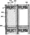
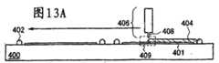
随后,利用液滴释放法形成闭合图案的密封剂381以包住与包含像素TFT的像素区域371重叠的区域(见图11A)。在此,由于液晶是滴入的,给出了闭合图案密封剂381的一例;但是,也可以使用浸入法(泵取法),其中设置具有开放部分的密封图案,然后在附着至衬底301后利用毛细现象注入液晶。Subsequently, a
接下来,在减压条件下滴下液晶367,以不使气泡进入(见图11B),TFT衬底301和对置衬底361附着在一起(见图11C)。液晶367一次或者多次在闭合循环密封图案中滴下。作为液晶367的取向模式,在许多情况下使用TN模式,其中液晶分子的排列从光线进入处到其存在处扭转90°。当制造TN模式的液晶显示装置时,衬底附着在一起使得衬底的摩擦方向相互垂直。Next,
注意衬底对之间的距离可以通过散置球状间隔件、形成树脂制成的柱状间隔件或者在密封剂381中包含填充物来保持。柱状间隔件为主要至少包含丙烯酸、聚酰亚胺、聚酰亚胺酰胺和环氧的至少一种的有机树脂;或者选自氧化硅、氮化硅或者含氮的氧化硅材料之一的单层膜或者它们的叠层膜的无机材料。Note that the distance between the pair of substrates can be maintained by interspersing spherical spacers, forming columnar spacers made of resin, or including a filler in the
随后,将衬底进行分割。在从衬底获得多个面板的情况下,每个面板被分离开。在从衬底获得单个面板的情况下,可以通过附着预先切割的对置衬底而跳过分割工序(见图11D)。Subsequently, the substrate is divided. Where multiple panels are obtained from a substrate, each panel is separated. In case a single panel is obtained from a substrate, the singulation process can be skipped by attaching a pre-cut counter substrate (see FIG. 11D ).
然后,利用已知技术通过各向异性导电层附着FPC(柔性印刷电路)。通过上述工序,就完成了本实施方式的液晶显示装置。另外,如果需要,附着光学膜。在透射型液晶显示装置的情况下,将偏振板附着至TFT衬底301以及对置衬底361的每个。Then, an FPC (Flexible Printed Circuit) is attached through an anisotropic conductive layer using a known technique. Through the above steps, the liquid crystal display device of this embodiment is completed. Also, attach optical film if desired. In the case of a transmission type liquid crystal display device, a polarizing plate is attached to each of the
通过上述工序获得的液晶显示装置的顶视图示于图12A,另一液晶显示装置的顶视图的一例示于图12B。A top view of a liquid crystal display device obtained through the above steps is shown in FIG. 12A , and an example of a top view of another liquid crystal display device is shown in FIG. 12B .
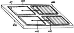
在图12A中,附图标记301、361、371、372、373、381和382分别表示TFT衬底、对置衬底、像素部分、源极信号线驱动电路、栅极信号线驱动电路、密封剂、和FPC。注意液晶通过液滴释放法释放,而成对的衬底301和对置衬底361通过减压条件下的密封剂381附着在一起。In FIG. 12A,
在图12B中,附图标记301、361、372、373、371、381a和382分别表示TFT衬底、对置衬底、源极信号线驱动电路、栅极信号线驱动电路、像素部分、第一密封剂和FPC。注意液晶通过液滴释放法释放,而成对的衬底301和对置衬底361通过第一密封剂381a和第二密封381b剂附着在一起。由于源极信号线驱动电路372和栅极信号线驱动电路373不需要液晶,液晶仅保持在像素部分371,而提供第二密封剂381b用于强化整个面板。In FIG. 12B,
以此方式,本实施方式的半导体器件的源区和漏区具有上下被源或漏电极夹在中间的结构;从而源或漏电极与半导体膜之间的接触电阻变小。同样由于具有两个源或漏电极层,连线电阻也变小。此外,由于形成于半导体膜下方的第一源或漏电极可形成得薄,半导体膜的覆盖率得到提高从而改善TFT特性,液晶显示装置整体的可靠性也得到提高。In this way, the source region and the drain region of the semiconductor device of this embodiment mode have a structure sandwiched up and down by the source or drain electrode; thus the contact resistance between the source or drain electrode and the semiconductor film becomes small. Also due to having two source or drain electrode layers, the wiring resistance is also reduced. In addition, since the first source or drain electrode formed under the semiconductor film can be formed thin, the coverage of the semiconductor film is improved to improve TFT characteristics, and the reliability of the liquid crystal display device as a whole is also improved.
另外,如果需要,本实施方式可以与实施方式1~4自由组合。In addition, this embodiment mode can be freely combined with Embodiment Modes 1 to 4 if necessary.
〔实施方式6〕[Embodiment 6]
在本实施方式中,对利用液滴释放法滴入液晶的一例进行说明。在本实施方式中,参照图13A~16B示出了利用大面积衬底400获得四块面板的制造例。In this embodiment, an example of dropping liquid crystals by a droplet discharge method will be described. In this embodiment mode, a manufacturing example in which four panels are obtained using a large-
图13A给出了加工过程中通过分配器(或者喷墨)形成液晶层的截面图,从液滴释放装置406的喷嘴释放、喷射或者滴出液晶材料404以覆盖由密封剂402包围的像素部分401。液滴释放装置406沿图13A中的箭头方向移动。注意尽管此处示出了移动喷嘴408的一例,液晶层也可以通过附着喷嘴并移动衬底形成。13A shows a cross-sectional view of a liquid crystal layer formed by a dispenser (or inkjet) during processing, releasing, spraying or dripping a
另外,图13B给出了透视图,其中示出了液晶材料404只被有选择地释放、喷射或者滴入由密封剂402包围的区域中,且滴入表面405沿喷嘴扫描方向403移动的情形。In addition, FIG. 13B shows a perspective view showing that the
另外,图13C和13D各给出了由图13A中的虚线包围的部分409的放大截面图。当液晶材料的粘性高时,液晶材料被连续释放,如图13C无间断地粘着。另一方面,当液晶材料的粘性低时,液晶材料被间断释放,如图13D液滴以点状滴下。In addition, FIGS. 13C and 13D each show an enlarged cross-sectional view of a
注意在图13C中,附图标记401和411分别表示根据本发明形成的像素TFT和像素电极。像素部分401包括矩阵形式放置的像素电极和连接至像素电极的开关元件,此处还包括底栅TFT和存储电容器。Note that in FIG. 13C,
以下参照图14A~15B对面板的制造流程进行说明。The manufacturing flow of the panel will be described below with reference to FIGS. 14A to 15B .
首先,准备具有在上面形成了像素部分401的绝缘表面的第一衬底400。对第一衬底400,预先进行取向膜的生成、摩擦处理、球形间隔件的散置或者柱状间隔件的形成、滤色器的形成等。其详细的制造方法参考实施方式5。First, a
随后,如图14A所示,通过在惰性气体或者低压下的分配装置或者喷墨装置在第一衬底400上方的预定位置(包围像素部分401的图案)形成密封剂402。对于半透明的密封剂402,使用包含填充剂(直径6μm~24μm)且粘性在40Pa·s至400Pa·s的材料。注意选定的材料最好不溶于随后接触的液晶,作为密封剂402,可使用丙烯酸基光固化树脂或者丙烯酸基热固化树脂。此外,由于是简单的密封图案,密封剂402可以通过印刷方法形成。Subsequently, as shown in FIG. 14A , a
接下来,通过喷墨法将液晶材料404滴入由密封剂402围住的区域(见图14B)。作为液晶材料404,可以使用已知的具有可以利用喷墨法释放的粘度的液晶材料。另外,由于液晶材料404的粘性可以通过调整温度来设置,所以适合于喷墨法。通过喷墨法,可以没有浪费地将所需量的液晶材料404存储在密封剂402围住的区域。Next,
随后,在减压状态下将上面设置了像素部分401的第一衬底400和上面设置了对置电极和取向膜的第二衬底421附着在一起,以不使气泡进入(见图15A)。在此,在将第一衬底400和第二衬底421附着在一起的同时,进行紫外线照射或者热处理,将密封剂402固化。注意可以在紫外线照射的同时进行热处理。Subsequently, the
另外,图16A和16B各自给出了在衬底附着期间或者之后能够进行紫外线照射或者热处理的附着装置的一例。In addition, FIGS. 16A and 16B each show an example of an attachment device capable of ultraviolet irradiation or heat treatment during or after substrate attachment.
在图16A和16B中,附图标记422、423、424、428和429分别表示第一衬底支撑基座、第二衬底支撑基座、光线传输窗、下侧测量板、紫外线光源。注意在图16A和16B中,相同的附图标记用于对应图13A~15B的相应部分。In FIGS. 16A and 16B ,
下侧测量板包括加热器,并固化密封剂402。另外,第二衬底支撑基座423设置有光线传输窗424并允许来自光源429的紫外线等透过。尽管此处未示出,通过窗424进行衬底的位置对准。此外,作为对置衬底的第二衬底421被预先切割成希望的尺寸并通过真空卡盘等附着至第二衬底支撑基座423。图16A给出了将第一衬底400和第二衬底421附着在一起之前的情形。The lower measurement plate includes a heater and cures the
在附着时,在向下移动第一衬底支撑基座422和第二衬底支撑基座423之后,第一衬底400和第二衬底421由压力附着在一起,然后通过紫外线照射按原样固化。在图16B中给出了将第一衬底400和第二衬底421附着在一起之后的情形。At the time of attachment, after moving down the first
随后,利用如划片装置、破开装置或者滚动切割机的切割装置切割第一衬底400(见图15B)。以此方式,可从一个衬底制造四块面板。然后利用已知技术附着FPC。Subsequently, the
注意,作为第一衬底400和第二衬底421可各自使用玻璃衬底或者塑料衬底。Note that a glass substrate or a plastic substrate may be used as the
以此方式,在本实施方式中,当利用液滴释放法制造液晶显示装置时,可以用到本发明的半导体器件。本发明的半导体器件的源区和漏区各自有上下被源或漏电极夹在中间的结构;从而源或漏电极与半导体膜之间的接触电阻变小。同样由于具有两个源或漏电极层,连线电阻也变小。此外,由于形成于半导体膜下方的第一源或漏电极可形成得薄,半导体膜的覆盖率得到提高从而改善TFT特性。液晶显示装置整体的可靠性也得到提高。In this way, in this embodiment mode, the semiconductor device of the present invention can be used when a liquid crystal display device is manufactured by the droplet discharge method. The source region and the drain region of the semiconductor device of the present invention each have a structure in which the source or drain electrode is sandwiched between the upper and lower sides; thus, the contact resistance between the source or drain electrode and the semiconductor film becomes small. Also due to having two source or drain electrode layers, the wiring resistance is also reduced. In addition, since the first source or drain electrode formed under the semiconductor film can be formed thin, the coverage of the semiconductor film is increased to improve TFT characteristics. The reliability of the liquid crystal display device as a whole is also improved.
此外,如果需要,本实施方式可与实施方式1~5自由组合。In addition, this embodiment mode can be freely combined with Embodiment Modes 1 to 5, if necessary.
〔实施方式7〕[Embodiment 7]
在本实施方式中,参照图17A~20对利用本发明制造双发射显示装置的一例进行说明。In this embodiment mode, an example of manufacturing a dual emission display device using the present invention will be described with reference to FIGS. 17A to 20 .
首先,基于实施方式1~4,在衬底501上形成n沟道TFT 561、562和p沟道TFT 563。First, n-channel TFTs 561, 562 and p-channel TFT 563 are formed on a substrate 501 based on Embodiment Modes 1 to 4.
n沟道TFT 561包括栅电极502,栅绝缘膜505,第一源或漏电极511和512,作为沟道形成区域的岛状半导体膜517,各自作为源区或漏区的岛状杂质半导体膜521和522,以及第二源或漏电极531和532。The n-channel TFT 561 includes a gate electrode 502, a gate insulating film 505, first source or drain electrodes 511 and 512, an island-shaped semiconductor film 517 as a channel formation region, island-shaped impurity semiconductor films each as a source region or a drain region 521 and 522, and the second source or drain electrodes 531 and 532.
n沟道TFT 562包括栅电极503,栅绝缘膜505,第一源或漏电极513和514,作为沟道形成区域的岛状半导体膜518,各自作为源区或漏区的岛状杂质半导体膜523和524,以及第二源或漏电极533和534。The n-channel TFT 562 includes a gate electrode 503, a gate insulating film 505, first source or drain electrodes 513 and 514, an island-shaped semiconductor film 518 as a channel formation region, island-shaped impurity semiconductor films each as a source region or a drain region 523 and 524, and the second source or drain electrodes 533 and 534.
p沟道TFT 563包括栅电极504,栅绝缘膜505,第一源或漏电极515和516,作为沟道形成区域的岛状半导体膜519,各自作为源区或漏区的岛状杂质半导体膜525和526,以及第二电极535和536。The p-channel TFT 563 includes a gate electrode 504, a gate insulating film 505, first source or drain electrodes 515 and 516, an island-shaped semiconductor film 519 as a channel formation region, and island-shaped impurity semiconductor films each as a source region or a drain region. 525 and 526, and the second electrodes 535 and 536.
作为衬底501,可以使用与本实施方式和实施方式1的衬底101相似的衬底。另外,可以参考本实施方式和实施方式1中的栅电极102、栅绝缘膜103、第一源或漏电极104、岛状半导体膜105和第二源或漏电极106,分别形成栅电极502~504,栅绝缘膜505,第一源或漏电极511~516,岛状半导体膜517~519,第二源或漏电极531~536。As the substrate 501 , a substrate similar to the
另外,n沟道TFT 561的岛状杂质半导体膜521和522以及n沟道TFT 562的岛状杂质半导体膜523和524的每个可以通过形成添加有赋予n型导电类型的杂质磷(P)或砷(As)的半导体膜形成。另一方面,p沟道TFT 563的岛状杂质半导体膜525和526的每个可以通过形成添加有赋予p型导电类型的杂质硼(B)的半导体膜形成。In addition, each of the island-shaped impurity semiconductor films 521 and 522 of the n-channel TFT 561 and the island-shaped impurity semiconductor films 523 and 524 of the n-channel TFT 562 can be formed by adding impurity phosphorus (P) which imparts n-type conductivity. Or arsenic (As) semiconductor film formation. On the other hand, each of the island-shaped impurity semiconductor films 525 and 526 of the p-channel TFT 563 can be formed by forming a semiconductor film to which boron (B) as an impurity imparting p-type conductivity is added.
在本实施方式中,p沟道TFT 563用作双发射显示装置的像素TFT。另外,n沟道TFT 561和562用作驱动像素TFT 563的驱动电路的TFT。注意,不要求像素TFT为p沟道TFT,也可使用n沟道TFT。此外,驱动电路不必为由多个n沟道TFT组合而成的电路,可以为n沟道TFT和p沟道TFT的互补地组合的电路,或者多个p沟道TFT组合而成的电路。In this embodiment mode, the p-channel TFT 563 is used as a pixel TFT of a dual emission display device. In addition, n-channel TFTs 561 and 562 are used as TFTs of a driving circuit that drives a pixel TFT 563. Note that the pixel TFT is not required to be a p-channel TFT, and an n-channel TFT may also be used. In addition, the driving circuit does not have to be a circuit composed of a plurality of n-channel TFTs, but may be a circuit composed of a complementary combination of n-channel TFTs and p-channel TFTs, or a circuit composed of a plurality of p-channel TFTs.
接下来,形成含氢的绝缘膜作为第一层间绝缘膜541。随后,激活被加入到岛状半导体膜的杂质元素。该杂质元素的激活可以通过实施方式5所述的激光处理法进行。Next, an insulating film containing hydrogen is formed as the first interlayer insulating film 541 . Subsequently, the impurity element added to the island-shaped semiconductor film is activated. Activation of this impurity element can be performed by the laser processing method described in the fifth embodiment.
作为含氢的绝缘膜,使用通过PCVD获得的含氮的氧化硅膜。或者使用含氧的氮化硅膜。注意第一层间绝缘膜541为具有光传输特性并包含氧化硅的绝缘膜。As the insulating film containing hydrogen, a silicon oxide film containing nitrogen obtained by PCVD is used. Alternatively, a silicon nitride film containing oxygen is used. Note that the first interlayer insulating film 541 is an insulating film having light transmission properties and containing silicon oxide.
随后,通过在410℃加热一小时进行岛状半导体膜的氢化。Subsequently, hydrogenation of the island-shaped semiconductor film was performed by heating at 410° C. for one hour.
接下来,形成作为第二层间绝缘膜542的平坦化膜。作为平坦化膜,可以使用具有光传输特性的无机材料(例如氧化硅,氮化硅,或者含氧的氮化硅)、感光或者非感光有机材料(例如聚酰亚胺、丙烯酸、聚酰胺、聚酰亚胺酰胺、抗蚀剂、或者苯并环丁烯)、或者它们的叠层。此外,作为具有光传输特性、用于平坦化膜的另一个膜可以使用通过涂敷法获得的、由含烃基的氧化硅膜制成的绝缘膜,例如利用硅玻璃、烷基硅氧烷聚合物、烷基硅倍半氧烷(alkylsilsesquioxane)聚合物、硅倍半氧烷(silsesquioxane)氢化聚合物、烷基硅倍半氧烷氢化聚合物等。作为基于硅氧烷(siloxane)聚合物的一例,给出由Toray industries Inc.生产的涂敷绝缘膜材料PSB-K1和PSB-K31和由Catalysts & Chemicals Industries Co.,Ltd.生产的涂敷绝缘膜材料ZRS-5PH。Next, a planarizing film is formed as the second interlayer insulating film 542 . As the planarization film, inorganic materials with light transmission characteristics (such as silicon oxide, silicon nitride, or silicon nitride containing oxygen), photosensitive or non-photosensitive organic materials (such as polyimide, acrylic, polyamide, polyimide amide, resist, or benzocyclobutene), or a laminate thereof. In addition, as another film having light-transmitting properties for a planarization film, an insulating film made of a silicon oxide film containing a hydrocarbon group obtained by a coating method, such as silicon glass, alkylsiloxane polymerization, etc., can be used. compounds, alkylsilsesquioxane polymers, silsesquioxane hydrogenated polymers, alkylsilsesquioxane hydrogenated polymers, etc. As an example of a siloxane-based polymer, coated insulating film materials PSB-K1 and PSB-K31 produced by Toray industries Inc. and coated insulating film materials produced by Catalysts & Chemicals Industries Co., Ltd. are given. Membrane material ZRS-5PH.
随后形成具有光传输特性的第三层间绝缘膜543。在后续的刻蚀作为第一像素电极565的导电膜的工序中,设置第三层间绝缘膜543作为刻蚀阻挡膜以保护作为平坦化膜的第二层间绝缘膜542。但是,如果在刻蚀作为第一像素电极565的导电膜时,第二层间绝缘膜542作为刻蚀阻挡膜,则不必设置第三层间绝缘膜543。A third interlayer insulating film 543 having light transmission properties is then formed. In the subsequent process of etching the conductive film serving as the first pixel electrode 565, the third interlayer insulating film 543 is provided as an etching stopper film to protect the second interlayer insulating film 542 serving as a planarization film. However, if the second interlayer insulating film 542 serves as an etching stopper when etching the conductive film serving as the first pixel electrode 565, it is not necessary to provide the third interlayer insulating film 543.
接下来,利用新的掩模穿过第一层间绝缘膜541、第二层间绝缘膜542、第三层间绝缘膜543形成接触孔。随后,去除该掩模,在形成导电膜(氮化钛膜、铝膜、氮化钛膜的叠层)之后,利用不同的掩模进行刻蚀(使用BCl3和Cl2的混合气体的干法刻蚀)以形成电极或连线551、电极或连线552、电极或连线553、电极或连线554、电极或连线555、电极或连线556(TFT的源极连线或者漏极连线、电流供给线等),统称电极或连线551~556(见图17A)。尽管电极和连线在本实施方式中一体地形成,电极和连线可以单独形成并电连接。注意氮化钛膜为与高热阻平坦化膜具有很好粘着性的材料之一。Next, contact holes are formed through the first interlayer insulating film 541 , the second interlayer insulating film 542 , and the third interlayer insulating film 543 using a new mask. Subsequently, this mask is removed, and after forming a conductive film (a stack of titanium nitride film, aluminum film, and titanium nitride film), etching is performed using a different mask (dry process using a mixed gas of BCl3 and Cl2 ). etching) to form electrodes or wiring 551, electrodes or wiring 552, electrodes or wiring 553, electrodes or wiring 554, electrodes or wiring 555, electrodes or wiring 556 (source wiring or drain of TFT Electrode connection lines, current supply lines, etc.), collectively referred to as electrodes or connection lines 551-556 (see Figure 17A). Although the electrodes and wiring are integrally formed in this embodiment, the electrodes and wiring may be formed separately and electrically connected. Note that the titanium nitride film is one of the materials that has good adhesion to the high thermal resistance planarization film.
随后,使用新的掩模形成第一像素电极565,以具有范围在10nm至800nm的厚度。作为第一像素电极565,可以使用具有高功函数(4.0eV的功函数或者更高)的透明导电膜,例如利用含硅元素的氧化铟锡的靶形成的导电膜、或者除氧化铟锡(ITO)靶之外混合有2~20Wt%氧化锌(ZnO)的氧化铟的靶形成的导电膜。Subsequently, the first pixel electrode 565 is formed using a new mask to have a thickness ranging from 10 nm to 800 nm. As the first pixel electrode 565, a transparent conductive film having a high work function (work function of 4.0 eV or higher), for example, a conductive film formed by using a target of indium tin oxide containing silicon, or an indium tin oxide ( A conductive film formed of an indium oxide target mixed with 2 to 20 wt% zinc oxide (ZnO) in addition to an ITO) target.
接下来,使用新的掩模形成覆盖第一像素电极565的末端部分的隔离件566(称为隔离物或者壁)。作为隔离件566,可以使用厚度在0.8μm~1μm、通过涂敷法得到的感光或者非感光有机材料(聚酰亚胺、丙烯酸、聚酰胺、聚酰亚胺酰胺、抗蚀剂、或者苯并环丁烯)、或者SOG膜(例如,含烷基团的氧化硅膜)。Next, a spacer 566 (referred to as a spacer or wall) covering an end portion of the first pixel electrode 565 is formed using a new mask. As the
随后通过蒸镀法或者涂敷法利用有机化合物形成空穴注入层571,空穴传输层572,发光层573,电子传输层574以及电子注入层575。Subsequently, a
注意空穴注入层571,空穴传输层572,发光层573,电子传输层574以及电子注入层575不一定要按此顺序形成,可以以下顺序在第一像素电极565和第二像素电极576之间从第一像素电极565一侧形成:电子注入层,电子传输层,发光层,空穴传输层,空穴注入层。Note that the
注意,为了提高发光元件的可靠性,最好在形成空穴注入层571之前通过真空加热去除气体。例如,在进行成为空穴注入层的有机化合物材料的蒸镀之前,最好在温度为200℃~300℃的减压气体或者惰性气体中进行热处理以去除包含在衬底中的气体。注意当利用具有高热阻的氧化硅膜形成层间绝缘膜和隔离件时,也可以进行高温(410℃)下的热处理。Note that, in order to improve the reliability of the light-emitting element, it is preferable to remove gas by vacuum heating before forming the
随后,利用蒸镀掩模通过共同蒸镀氧化钼(MoOx)、4-4’-二[N-(1-萘基)-N-苯基-氨基]-联苯(α-NPD)和红荧烯(rubrene),在第一像素电极565上有选择地形成空穴注入层(包含有机化合物的第一层)571。Subsequently, molybdenum oxide (MoOx), 4-4'-bis[N-(1-naphthyl)-N-phenyl-amino]-biphenyl (α-NPD) and red A hole injection layer (a first layer including an organic compound) 571 is selectively formed on the first pixel electrode 565 using rubrene.
注意除MoOx外,还可以使用具有较高的空穴注入特性的材料,如酞菁铜(CuPc)、氧化钒(Vox)、氧化钌(RuOx)或者氧化钨(WOx)。另外,空穴注入层571还可通过涂敷法利用具有高空穴注入特性的高分子化合物材料形成,例如聚乙烯基二氧噻吩(poly(ethylene dioxythiophene))/聚乙烯基二氧噻吩/聚苯乙烯磺酸(poly(styrenesulfonic acid))溶液(PEDOT/PSS)。Note that other than MoOx, a material having a higher hole injection property such as copper phthalocyanine (CuPc), vanadium oxide (Vox), ruthenium oxide (RuOx), or tungsten oxide (WOx) can be used. In addition, the
接下来,利用蒸镀掩模有选择地蒸镀α-NPD以在空穴注入层571上方形成空穴传输层(包含有机化合物的第二层)572。注意除α-NPD外还可使用具有高空穴传输特性的以芳香胺化合物为代表的有机化合物,例如4,4’-二[N-(3-甲基苯基)-N-苯基氨基]联苯(缩写:TPD),4,4’4”-三(N,N-二苯基-氨基)-三苯胺(缩写TDATA),或者4,4’,4”-三[N-(3-甲基-苯基)-N-苯基-氨基]-三苯胺(缩写MTDATA)。Next, α-NPD was selectively evaporated using an evaporation mask to form a hole transport layer (second layer containing an organic compound) 572 over the
随后有选择地形成发光层(包含有机化合物的第三层)573。对于全色显示装置,为每个发光色(R、G、B)对准蒸镀掩模,然后进行有选择地蒸镀。A light emitting layer (third layer containing an organic compound) 573 is then selectively formed. For a full-color display device, an evaporation mask is aligned for each luminescent color (R, G, B), and then selectively evaporated.
作为发红光的发光层573R,使用如Alq3:DCM或者Alq3:红荧烯:BisDCJTM的材料。另外,对于发绿光的发光层573G,使用如Alq3:DMDQ(N,N’-二甲基喹吖酮)或者Alq3:香豆素6的材料。此外对于发蓝光的发光层573B,使用如α-NPD或者tBu-DNA的材料。As the red-emitting light-emitting
接下来利用蒸镀掩模有选择地蒸镀Alq3(三(8-羟基喹啉)铝)以在发光层573上方形成电子传输层(含有机化合物的第四层)574。另外,除Alq3外,还可以使用具有高电子运输性能的、以具有喹啉骨架或者苯并喹啉骨架的金属合成物为代表的有机化合物,例如三(5-甲基-8-羟基喹啉)铝(缩写:Almq3),二(10-羟基苯[h]-羟基喹啉)铍(缩写:BeBq2),二(2-甲基-8-羟基喹啉)-4-苯基酚氧-铝(缩写:BAlq)等。此外,还可使用具有噁唑基或者噻唑基配合体(ligand)的金属合成物,例如二[2-(2-羟基苯基)-苯并噁唑]锌(缩写:Zn(BOX)2),或者二[2-(2-羟基苯基)-苯并噻唑]锌(缩写:Zn(BTZ)2)。此外,除金属合成物,还可使用同样具有高电子运输特性的材料作为电子传输层574,例如2-(4-二苯基)-5-(4-叔丁基苯基)-1,3,4-噁二唑(缩写:PBD)、1,3-二[5-(p-叔丁基苯基)-1,3,4-噁二唑-2-基]苯(缩写:OXD-7),3-(4-叔丁基苯基)-4-苯基-5-(4-二苯基)-1,2,4-三唑(缩写:TAZ)、3-(4-叔丁基苯基)-4-(4-乙烯基苯基)-5-(4-二苯基)-1,2,4-三唑(缩写:p-EtTAZ)、向红菲咯啉(缩写:BPhen)、浴铜灵(缩写BCP)等。Next, Alq3 (tris(8-quinolinolato)aluminum) is selectively evaporated using an evaporation mask to form an electron transport layer (fourth layer containing an organic compound) 574 over the
接下来,共同蒸镀4,4-二(5-甲基苯并噁唑-2-基)茋(缩写:BzOs)和锂(Li)以形成覆盖电子传输层574和隔离件566的电子注入层575(含有机化合物的第五层)。通过使用苯并噁唑衍生物(BzOs),可以抑制在以后的工序中进行的形成第二像素电极576期间因溅射法造成的损坏。同样除了BxOs:Li之外,还可以使用具有高电子注入特性的材料,例如碱金属或者碱土金属的化合物,例如CaF2,氟化锂(LiF)、氟化铯(CsF)等。此外,Alq3和镁(Mg)的混合物亦可使用。Next, 4,4-bis(5-methylbenzoxazol-2-yl)stilbene (abbreviation: BzOs) and lithium (Li) are co-evaporated to form an electron injection layer covering the
随后,在电子注入层575上形成厚度为10nm~800nm的第二像素电极576。作为第二像素电极576,可以使用利用含硅元素的氧化铟锡的靶形成的导电膜,或者除氧化铟锡(ITO)之外混合有2~20Wt%氧化锌(ZnO)的氧化铟的靶形成的导电膜。Subsequently, a
以上述方式制成发光元件。构成发光元件的第一像素电极565、空穴注入层571、空穴传输层572、发光层573、电子传输层574、电子注入层575和第二像素电极576的材料和厚度被适当地选定和设定。第一和第二像素电极优选使用相同的材料,并具有大致相同的膜厚,优选为100nm厚。A light-emitting element was fabricated in the manner described above. The materials and thicknesses of the first pixel electrode 565, the
另外,如上所述,如果需要,第一像素电极565、电子注入层、电子传输层、发光层、空穴传输层、空穴注入层和第二像素电极576可以此顺序叠层。In addition, as described above, the first pixel electrode 565, the electron injection layer, the electron transport layer, the light emitting layer, the hole transport layer, the hole injection layer, and the
此外,如果需要,覆盖发光元件形成防止湿气进入的透明保护层577。作为透明保护层577,可以使用通过溅射法或者CVD法得到的氮化硅膜、氧化硅膜、含氧的氮化硅膜、含氮的氧化硅膜、主要包含碳(例如类金刚石碳膜(DLC)或者氮化碳(CN)膜)的薄膜等(见图18)。In addition, if necessary, a transparent
此外,利用包含用来保持衬底之间的间距的间隙材料的密封剂将衬底581和衬底501附着在一起。第二衬底581也可以由具有光传输特性的玻璃衬底或者石英衬底形成。注意在成对的衬底之间的空间里可以放置干燥剂作为气隙(惰性气体),或者在成对的衬底之间填入透明密封剂(例如紫外线固化或者热固化环氧树脂)。In addition, the
由于发光元件的第一像素电极565和第二像素电极576由光传输材料形成,光可以沿两个方向发射,换言之,从单个发光元件的两面发光。Since the first pixel electrode 565 and the
利用上述面板结构,从上表面和下表面发出的光的强度可以大致相同。With the above panel structure, the intensity of light emitted from the upper surface and the lower surface can be approximately the same.
最后,分别在衬底501和581上提供光学膜(偏振板或者圆偏振板)582和583,以提高对比度(见图19)。Finally, optical films (polarizing plates or circular polarizing plates) 582 and 583 are provided on the
图20给出了各个发光色(红(R)、绿(G)、蓝(B))的发光元件的截面图。发红光元件(R)包括像素TFT 563R、第一像素电极565R、空穴注入层571R、空穴传输层572R、发光层573R、电子传输层574R、电子注入层575、第二像素电极576和透明保护层577。FIG. 20 shows cross-sectional views of light-emitting elements of respective light-emitting colors (red (R), green (G), blue (B)). The red light emitting element (R) includes a
另外,发绿光元件(R)包括像素TFT 563G、第一像素电极565G、空穴注入层571G、空穴传输层572G、发光层573G、电子传输层574G、电子注入层575、第二像素电极576和透明保护层577。In addition, the green light emitting element (R) includes a
另外,发蓝光元件(B)包括像素TFT 563B、第一像素电极565B、空穴注入层571B、空穴传输层572B、发光层573B、电子传输层574B、电子注入层575、第二像素电极576和透明保护层577。In addition, the blue light-emitting element (B) includes a
以此方式,本实施方式的半导体器件的源区和漏区各具有上下被源或漏电极夹在中间的结构;从而源或漏电极与半导体膜之间的接触电阻变小。同样由于具有两个源或漏电极层,连线电阻也变小。此外,由于形成于半导体膜下方的第一源或漏电极可形成得薄,半导体膜的覆盖率得到提高从而改善TFT特性,双发射显示装置整体的可靠性也得到提高。In this way, the source region and the drain region of the semiconductor device of this embodiment mode each have a structure sandwiched up and down by the source or drain electrode; thus the contact resistance between the source or drain electrode and the semiconductor film becomes small. Also due to having two source or drain electrode layers, the wiring resistance is also reduced. In addition, since the first source or drain electrode formed under the semiconductor film can be formed thin, the coverage of the semiconductor film is improved to improve TFT characteristics, and the overall reliability of the dual emission display device is also improved.
此外,如果需要,本实施方式可以与实施方式1~6自由组合。In addition, this embodiment mode can be freely combined with Embodiment Modes 1 to 6, if necessary.
〔实施方式8〕[Embodiment 8]
作为应用本发明的电器,给出如下:如摄像机和数码相机的照相机,护目镜式显示器,导航系统,音频播放装置(例如汽车音响),计算机,游戏机,便携式信息终端(例如移动计算机,蜂窝电话,便携式游戏机和电子书),设有记录介质的图像播放装置(具体地,可以播放诸如数码通用光盘(DVD)的记录介质的装置以及包括能够显示图像的显示装置)等。这些电器的具体例示于图21A、22D。As the electrical appliances to which the present invention is applied, the following are given: cameras such as video cameras and digital cameras, goggle displays, navigation systems, audio playback devices (such as car stereos), computers, game machines, portable information terminals (such as mobile computers, cellular telephones, portable game machines, and electronic books), image playback devices provided with recording media (specifically, devices that can play back recording media such as Digital Versatile Discs (DVD) and display devices that include images capable of displaying images), and the like. Specific examples of these electric appliances are shown in Figs. 21A and 22D.
图21A给出了电视接收机等对应的发光显示装置。该发光显示装置包括外壳601、显示部分603、扬声器部分604等。本发明可应用于显示部分603、控制电路部分等。极化极板或者圆偏振板可以设在像素部分中以提高对比度。例如可以在密封衬底上以1/4λ板、1/2λ板和偏振板的顺序设置。另外,可以在偏振板上方设置抗反射膜。通过利用本发明,可以获得具有高可靠性的发光显示装置。FIG. 21A shows a corresponding light-emitting display device such as a television receiver. This light-emitting display device includes a
图21B给出了液晶显示器或者EL显示器,包括外壳611,支撑基座612,显示部分613等。本发明可应用于显示部分613、控制电路部分等。利用本发明,可以得到具有高可靠性的液晶显示器或EL显示器。FIG. 21B shows a liquid crystal display or an EL display including a
图21C给出了蜂窝电话,包括主体621,外壳622,显示部分623,音频输入部分624,音频输出部分625,操作键626,天线628等。本发明可应用于显示部分623和控制电路部分等。利用本发明,可以获得具有高可靠性的蜂窝电话。FIG. 21C shows a cellular phone including a
图21D给出了个人计算机,包括主体631,外壳632,显示部分633,键盘634,外部连接端口635,连接鼠标636等。本发明可应用于显示部分633和控制电路部分等。利用本发明,可以获得具有高可靠性的个人电脑。FIG. 21D shows a personal computer including a
图22A给出了移动计算机,包括主体651,显示部分652,开关653,操作键654,红外端口655等。本发明可应用于显示部分652和控制电路部分等。利用本发明,可以获得具有高可靠性的移动电脑。FIG. 22A shows a mobile computer including a
图22B给出了便携式游戏机,包括外壳661,显示部分662,扬声器部分663,操作键664,记录介质插入部分665等。本发明可应用于显示部分662和控制电路部分等。利用本发明,可以获得具有高可靠性的便携式游戏机。FIG. 22B shows a portable game machine including a
图22C给出了设有记录介质的便携式图像播放装置(具体地,DVD播放装置),包括主体671,外壳672,显示部分A 673,显示部分B 674,读取诸如DVD的记录介质的记录介质读取部分675,操作键676,扬声器部分677等。显示部分A 673主要显示图像信息,显示部分B 674主要显示文本信息。本发明可应用于显示部分A 673、显示部分B 674和控制电路部分等。注意家用游戏机等也包括在设有记录介质的图像播放装置中。利用本发明,可以获得具有高可靠性的图像播放装置。Fig. 22 C has provided the portable image playback device (specifically, DVD playback device) that is provided with recording medium, comprises main body 671, casing 672, display part A 673, display part B 674, reads the recording medium of the recording medium such as DVD A reading section 675, operation keys 676, a speaker section 677, and the like. The display part A 673 mainly displays image information, and the display part B 674 mainly displays text information. The present invention can be applied to the display part A 673, the display part B 674, the control circuit part, and the like. Note that home game machines and the like are also included in the image playback device provided with the recording medium. With the present invention, an image playback device with high reliability can be obtained.
图22D给出了显示器可以四处携带的无线电视。在外壳682中包含电池和信号接收器,显示部分683和扬声器部分687由该电池驱动。电池可以通过充电器681反复充电。此外,充电器681还可以传输和接收图像信号,并将图像信号传输至显示装置的接收器。外壳682由操作键686控制。另外,图22D所示的装置也可以称为音视频双向通讯装置,因其可以通过操作操作键686将信号从外壳682传输至充电器681。此外,图22D所示装置也可称为通用遥控装置,因其可以通过操作操作键686和从外壳682向充电器681发送信号以及使其他电器接收从充电器681传输的信号,来控制另一电器的通讯。本发明可应用于显示部分683和控制电路部分等。利用本发明,可以获得具有高可靠性的TV。Figure 22D shows a wireless television with a display that can be carried around. A battery and a signal receiver are contained in the
注意本实施方式中所示例子仅为示例,并不限于这些应用。Note that the examples shown in this embodiment mode are only examples and are not limited to these applications.
以此方式,本实施方式的半导体器件的源区和漏区各具有上下被源或漏电极夹在中间的结构;从而源或漏电极与半导体膜之间的接触电阻变小。同样由于具有两个源或漏电极层,连线电阻也变小。此外,由于形成于半导体膜下方的第一源或漏电极可形成得薄,半导体膜的覆盖率得到提高从而改善TFT特性,包含本发明半导体器件的各个电器整体的可靠性也得到提高。In this way, the source region and the drain region of the semiconductor device of this embodiment mode each have a structure sandwiched up and down by the source or drain electrode; thus the contact resistance between the source or drain electrode and the semiconductor film becomes small. Also due to having two source or drain electrode layers, the wiring resistance is also reduced. In addition, since the first source or drain electrode formed under the semiconductor film can be formed thin, the coverage of the semiconductor film is improved to improve TFT characteristics, and the reliability of each electric device including the semiconductor device of the present invention is also improved as a whole.
此外,如果需要,本实施方式可以与实施方式1~7自由组合。In addition, this embodiment mode can be freely combined with Embodiment Modes 1 to 7, if necessary.
工业适用性Industrial applicability
通过本发明可以获得源或漏电极和半导体膜之间的接触电阻减小的半导体器件。这是由于本发明的半导体器件的源区或漏区具有上下被源或漏电极夹在中间的结构。A semiconductor device having reduced contact resistance between a source or drain electrode and a semiconductor film can be obtained by the present invention. This is because the source region or the drain region of the semiconductor device of the present invention has a structure in which the upper and lower sides are sandwiched by the source or drain electrodes.
另外,由于在本发明的半导体器件中形成两个源或漏电极层,一个在电阻半导体膜上方,另一个在电阻半导体膜下方,连线电阻得以减小。In addition, since two source or drain electrode layers are formed in the semiconductor device of the present invention, one above and the other below the resistive semiconductor film, wiring resistance can be reduced.
此外,在本发明的半导体器件中,由于形成于半导体膜下方的第一源或漏电极可形成得薄,半导体膜的覆盖率得到提高从而改善TFT特性。通过以上,本发明的半导体器件的可靠性也得到提高。Furthermore, in the semiconductor device of the present invention, since the first source or drain electrode formed under the semiconductor film can be formed thin, the coverage of the semiconductor film is increased to improve TFT characteristics. Through the above, the reliability of the semiconductor device of the present invention is also improved.
本发明基于2005年10月14日提出的日本专利在先申请第2005-300825号并要求其优先权,其所有内容通过引用包含于此。This application is based on and claims priority from Japanese Patent Priority Application No. 2005-300825 filed on October 14, 2005, the entire contents of which are hereby incorporated by reference.
Claims (10)
Applications Claiming Priority (3)
| Application Number | Priority Date | Filing Date | Title |
|---|---|---|---|
| JP2005300825 | 2005-10-14 | ||
| JP300825/2005 | 2005-10-14 | ||
| PCT/JP2006/320154WO2007043493A1 (en) | 2005-10-14 | 2006-10-03 | Semiconductor device and manufacturing method thereof |
Publications (2)
| Publication Number | Publication Date |
|---|---|
| CN101278403A CN101278403A (en) | 2008-10-01 |
| CN101278403Btrue CN101278403B (en) | 2010-12-01 |
Family
ID=37942733
Family Applications (1)
| Application Number | Title | Priority Date | Filing Date |
|---|---|---|---|
| CN2006800364073AExpired - Fee RelatedCN101278403B (en) | 2005-10-14 | 2006-10-03 | Semiconductor device and manufacturing method thereof |
Country Status (5)
| Country | Link |
|---|---|
| US (4) | US7749825B2 (en) |
| EP (1) | EP1935027B1 (en) |
| JP (3) | JP5504317B2 (en) |
| CN (1) | CN101278403B (en) |
| WO (1) | WO2007043493A1 (en) |
Cited By (1)
| Publication number | Priority date | Publication date | Assignee | Title |
|---|---|---|---|---|
| US8912040B2 (en) | 2008-10-22 | 2014-12-16 | Semiconductor Energy Laboratory Co., Ltd. | Method for manufacturing semiconductor device |
Families Citing this family (59)
| Publication number | Priority date | Publication date | Assignee | Title |
|---|---|---|---|---|
| KR20070053060A (en)* | 2005-11-19 | 2007-05-23 | 삼성전자주식회사 | Display device and manufacturing method thereof |
| US8202771B2 (en)* | 2006-09-26 | 2012-06-19 | Dai Nippon Printing Co., Ltd. | Manufacturing method of organic semiconductor device |
| JP2008147418A (en)* | 2006-12-11 | 2008-06-26 | Hitachi Ltd | Thin film transistor device, image display device and manufacturing method thereof |
| US7738050B2 (en)* | 2007-07-06 | 2010-06-15 | Semiconductor Energy Laboratory Co., Ltd | Liquid crystal display device |
| KR100936874B1 (en)* | 2007-12-18 | 2010-01-14 | 삼성모바일디스플레이주식회사 | Method for manufacturing thin film transistor and method for manufacturing organic light emitting display device comprising thin film transistor |
| KR20090074561A (en)* | 2008-01-02 | 2009-07-07 | 주식회사 하이닉스반도체 | Contact formation method of semiconductor device |
| WO2009157284A1 (en)* | 2008-06-24 | 2009-12-30 | 国立大学法人九州工業大学 | Organic field effect transistor |
| KR20100009869A (en)* | 2008-07-21 | 2010-01-29 | 삼성전자주식회사 | Cmos transistor and method of manufacturing the same |
| TWI627757B (en) | 2008-07-31 | 2018-06-21 | 半導體能源研究所股份有限公司 | Semiconductor device |
| CN102160184B (en) | 2008-09-19 | 2014-07-09 | 株式会社半导体能源研究所 | Display device |
| KR101643204B1 (en)* | 2008-12-01 | 2016-07-27 | 가부시키가이샤 한도오따이 에네루기 켄큐쇼 | Semiconductor device and manufacturing method thereof |
| TW201023341A (en)* | 2008-12-12 | 2010-06-16 | Ind Tech Res Inst | Integrated circuit structure |
| CN103456794B (en) | 2008-12-19 | 2016-08-10 | 株式会社半导体能源研究所 | How Transistors Are Made |
| US8383470B2 (en) | 2008-12-25 | 2013-02-26 | Semiconductor Energy Laboratory Co., Ltd. | Thin film transistor (TFT) having a protective layer and manufacturing method thereof |
| JP2010182819A (en)* | 2009-02-04 | 2010-08-19 | Sony Corp | Thin-film transistor, and display device |
| US8841661B2 (en) | 2009-02-25 | 2014-09-23 | Semiconductor Energy Laboratory Co., Ltd. | Staggered oxide semiconductor TFT semiconductor device and manufacturing method thereof |
| US20100224880A1 (en)* | 2009-03-05 | 2010-09-09 | Semiconductor Energy Laboratory Co., Ltd. | Semiconductor device |
| JP5429454B2 (en)* | 2009-04-17 | 2014-02-26 | ソニー株式会社 | Thin film transistor manufacturing method and thin film transistor |
| KR101904811B1 (en) | 2009-07-24 | 2018-10-05 | 가부시키가이샤 한도오따이 에네루기 켄큐쇼 | Semiconductor device |
| WO2011027676A1 (en) | 2009-09-04 | 2011-03-10 | Semiconductor Energy Laboratory Co., Ltd. | Semiconductor device and manufacturing method thereof |
| WO2011027701A1 (en) | 2009-09-04 | 2011-03-10 | Semiconductor Energy Laboratory Co., Ltd. | Light-emitting device and method for manufacturing the same |
| CN104681447A (en) | 2009-09-04 | 2015-06-03 | 株式会社半导体能源研究所 | Manufacturing Method Of Semiconductor Device |
| KR20120068772A (en) | 2009-09-16 | 2012-06-27 | 가부시키가이샤 한도오따이 에네루기 켄큐쇼 | Light-emitting device and manufacturing method thereof |
| KR20230165355A (en) | 2009-09-16 | 2023-12-05 | 가부시키가이샤 한도오따이 에네루기 켄큐쇼 | Display device |
| JP5565609B2 (en)* | 2009-10-02 | 2014-08-06 | ソニー株式会社 | Manufacturing method of semiconductor device |
| KR102143040B1 (en) | 2009-10-16 | 2020-08-11 | 가부시키가이샤 한도오따이 에네루기 켄큐쇼 | Liquid crystal display device and electronic apparatus having the same |
| CN107731931B (en) | 2009-10-21 | 2021-03-23 | 株式会社半导体能源研究所 | Display device and electronic equipment including display device |
| KR102162746B1 (en) | 2009-10-21 | 2020-10-07 | 가부시키가이샤 한도오따이 에네루기 켄큐쇼 | Analog circuit and semiconductor device |
| KR101751908B1 (en) | 2009-10-21 | 2017-06-28 | 가부시키가이샤 한도오따이 에네루기 켄큐쇼 | Voltage regulator circuit |
| KR102148664B1 (en) | 2009-11-06 | 2020-08-28 | 가부시키가이샤 한도오따이 에네루기 켄큐쇼 | Semiconductor device and manufacturing method thereof |
| WO2011068025A1 (en)* | 2009-12-04 | 2011-06-09 | Semiconductor Energy Laboratory Co., Ltd. | Dc converter circuit and power supply circuit |
| WO2011089841A1 (en)* | 2010-01-22 | 2011-07-28 | Semiconductor Energy Laboratory Co., Ltd. | Semiconductor device |
| KR102420689B1 (en) | 2010-02-26 | 2022-07-15 | 가부시키가이샤 한도오따이 에네루기 켄큐쇼 | Semiconductor device |
| KR20110101771A (en)* | 2010-03-09 | 2011-09-16 | 삼성모바일디스플레이주식회사 | Organic light emitting display |
| KR20130045418A (en) | 2010-04-23 | 2013-05-03 | 가부시키가이샤 한도오따이 에네루기 켄큐쇼 | Manufacturing method of semiconductor device |
| KR101995851B1 (en) | 2010-07-02 | 2019-07-03 | 가부시키가이샤 한도오따이 에네루기 켄큐쇼 | Semiconductor device |
| TWI541782B (en) | 2010-07-02 | 2016-07-11 | 半導體能源研究所股份有限公司 | Liquid crystal display device |
| TWI427784B (en)* | 2010-07-16 | 2014-02-21 | Au Optronics Corp | Method for manufacturing pixel structure and method for manufacturing organic light emitting device |
| WO2012029644A1 (en)* | 2010-08-30 | 2012-03-08 | シャープ株式会社 | Semiconductor device and process for production thereof |
| WO2013018137A1 (en)* | 2011-08-03 | 2013-02-07 | パナソニック株式会社 | Display panel device and method for manufacturing same |
| US10026847B2 (en) | 2011-11-18 | 2018-07-17 | Semiconductor Energy Laboratory Co., Ltd. | Semiconductor element, method for manufacturing semiconductor element, and semiconductor device including semiconductor element |
| TWI445181B (en)* | 2012-02-08 | 2014-07-11 | E Ink Holdings Inc | Thin film transistor |
| JP6103854B2 (en)* | 2012-08-10 | 2017-03-29 | 三菱電機株式会社 | Thin film transistor substrate |
| US9853053B2 (en) | 2012-09-10 | 2017-12-26 | 3B Technologies, Inc. | Three dimension integrated circuits employing thin film transistors |
| JP2015115469A (en) | 2013-12-12 | 2015-06-22 | ソニー株式会社 | THIN FILM TRANSISTOR, DISPLAY DEVICE, ELECTRONIC DEVICE, AND METHOD FOR PRODUCING THIN FILM TRANSISTOR |
| WO2016099580A2 (en) | 2014-12-23 | 2016-06-23 | Lupino James John | Three dimensional integrated circuits employing thin film transistors |
| CN105161544A (en) | 2015-10-16 | 2015-12-16 | 深圳市华星光电技术有限公司 | Thin-film field effect transistor, manufacturing method thereof, and LCD |
| CN105895534B (en)* | 2016-06-15 | 2018-10-19 | 武汉华星光电技术有限公司 | The preparation method of thin film transistor (TFT) |
| CN106328592A (en)* | 2016-10-27 | 2017-01-11 | 京东方科技集团股份有限公司 | Thin film transistor and manufacturing method, the array substrate and display device |
| US10424670B2 (en) | 2016-12-30 | 2019-09-24 | Intel Corporation | Display panel with reduced power consumption |
| US11177356B2 (en) | 2017-08-31 | 2021-11-16 | Boe Technology Group Co., Ltd. | Thin film transistor, array substrate, display apparatus, and method of fabricating thin film transistor |
| JP6553693B2 (en)* | 2017-09-14 | 2019-07-31 | 株式会社半導体エネルギー研究所 | Semiconductor device |
| DE112018005420T5 (en) | 2018-01-10 | 2020-07-30 | Intel Corporation | THIN FILM TRANSISTORS WITH LOW CONTACT RESISTANCE |
| CN109037350A (en)* | 2018-08-01 | 2018-12-18 | 深圳市华星光电半导体显示技术有限公司 | Thin film transistor (TFT) and preparation method thereof, array substrate |
| KR20220006541A (en) | 2019-05-10 | 2022-01-17 | 가부시키가이샤 한도오따이 에네루기 켄큐쇼 | Display devices and electronic devices |
| CN110998857A (en)* | 2019-11-27 | 2020-04-10 | 重庆康佳光电技术研究院有限公司 | A kind of thin film transistor and its preparation method and thin film transistor array |
| JP7732465B2 (en)* | 2020-11-13 | 2025-09-02 | コニカミノルタ株式会社 | Printing method and inkjet recording device |
| CN112530978B (en)* | 2020-12-01 | 2024-02-13 | 京东方科技集团股份有限公司 | Switching device structure and preparation method thereof, thin film transistor film layer, display panel |
| TWI874110B (en)* | 2024-01-19 | 2025-02-21 | 新唐科技股份有限公司 | Planarization method for imd in gan metal-insulator-semiconductor high-electron-mobility transistor (mis-hemt) and mis-hemt using the same |
Citations (1)
| Publication number | Priority date | Publication date | Assignee | Title |
|---|---|---|---|---|
| US6403408B1 (en)* | 1999-08-24 | 2002-06-11 | U.S. Philips Corporation | Thin-film transistors and method for producing the same |
Family Cites Families (84)
| Publication number | Priority date | Publication date | Assignee | Title |
|---|---|---|---|---|
| US4065781A (en)* | 1974-06-21 | 1977-12-27 | Westinghouse Electric Corporation | Insulated-gate thin film transistor with low leakage current |
| US4381213A (en)* | 1980-12-15 | 1983-04-26 | Motorola, Inc. | Partial vacuum boron diffusion process |
| JPS60198861A (en) | 1984-03-23 | 1985-10-08 | Fujitsu Ltd | Thin film transistor |
| JPS6151188A (en)* | 1984-08-21 | 1986-03-13 | セイコーインスツルメンツ株式会社 | Substrate for active matrix display unit |
| JPH0244256B2 (en) | 1987-01-28 | 1990-10-03 | Kagaku Gijutsucho Mukizaishitsu Kenkyushocho | INGAZN2O5DESHIMESARERUROTSUHOSHOKEINOSOJOKOZOOJUSURUKAGOBUTSUOYOBISONOSEIZOHO |
| JPH0244260B2 (en) | 1987-02-24 | 1990-10-03 | Kagaku Gijutsucho Mukizaishitsu Kenkyushocho | INGAZN5O8DESHIMESARERUROTSUHOSHOKEINOSOJOKOZOOJUSURUKAGOBUTSUOYOBISONOSEIZOHO |
| JPS63210023A (en) | 1987-02-24 | 1988-08-31 | Natl Inst For Res In Inorg Mater | Compound having a hexagonal layered structure represented by InGaZn↓4O↓7 and its manufacturing method |
| JPH0244258B2 (en) | 1987-02-24 | 1990-10-03 | Kagaku Gijutsucho Mukizaishitsu Kenkyushocho | INGAZN3O6DESHIMESARERUROTSUHOSHOKEINOSOJOKOZOOJUSURUKAGOBUTSUOYOBISONOSEIZOHO |
| JPH0244262B2 (en) | 1987-02-27 | 1990-10-03 | Kagaku Gijutsucho Mukizaishitsu Kenkyushocho | INGAZN6O9DESHIMESARERUROTSUHOSHOKEINOSOJOKOZOOJUSURUKAGOBUTSUOYOBISONOSEIZOHO |
| JPH0244263B2 (en) | 1987-04-22 | 1990-10-03 | Kagaku Gijutsucho Mukizaishitsu Kenkyushocho | INGAZN7O10DESHIMESARERUROTSUHOSHOKEINOSOJOKOZOOJUSURUKAGOBUTSUOYOBISONOSEIZOHO |
| JPH0687466B2 (en)* | 1988-07-13 | 1994-11-02 | 株式会社精工舎 | Silicon thin film transistor and method of manufacturing silicon thin film transistor |
| US5125945A (en) | 1991-04-09 | 1992-06-30 | Corning Incorporated | Method and apparatus for parallel alignment of opposing mold surfaces by controlling the thermal expansion of the apparatus |
| JP3277548B2 (en) | 1991-05-08 | 2002-04-22 | セイコーエプソン株式会社 | Display board |
| JP3255942B2 (en) | 1991-06-19 | 2002-02-12 | 株式会社半導体エネルギー研究所 | Method for manufacturing inverted staggered thin film transistor |
| JPH05251705A (en) | 1992-03-04 | 1993-09-28 | Fuji Xerox Co Ltd | Thin-film transistor |
| JPH07131019A (en) | 1993-11-01 | 1995-05-19 | Nec Corp | Thin film transistor and fabrication thereof |
| JP3479375B2 (en) | 1995-03-27 | 2003-12-15 | 科学技術振興事業団 | Metal oxide semiconductor device in which a pn junction is formed with a thin film transistor made of a metal oxide semiconductor such as cuprous oxide, and methods for manufacturing the same |
| KR100394896B1 (en) | 1995-08-03 | 2003-11-28 | 코닌클리케 필립스 일렉트로닉스 엔.브이. | A semiconductor device including a transparent switching element |
| JP3409542B2 (en)* | 1995-11-21 | 2003-05-26 | ソニー株式会社 | Method for manufacturing semiconductor device |
| JP3625598B2 (en) | 1995-12-30 | 2005-03-02 | 三星電子株式会社 | Manufacturing method of liquid crystal display device |
| KR100269326B1 (en)* | 1998-06-08 | 2000-10-16 | 윤종용 | Capacitor having electrode formed by electroplating and method for manufacturing the same |
| JP4170454B2 (en) | 1998-07-24 | 2008-10-22 | Hoya株式会社 | Article having transparent conductive oxide thin film and method for producing the same |
| JP2000150861A (en) | 1998-11-16 | 2000-05-30 | Tdk Corp | Oxide thin film |
| JP3276930B2 (en)* | 1998-11-17 | 2002-04-22 | 科学技術振興事業団 | Transistor and semiconductor device |
| TW460731B (en) | 1999-09-03 | 2001-10-21 | Ind Tech Res Inst | Electrode structure and production method of wide viewing angle LCD |
| US6580127B1 (en)* | 1999-09-30 | 2003-06-17 | International Business Machines Corporation | High performance thin film transistor and active matrix process for flat panel displays |
| JP4630420B2 (en) | 2000-05-23 | 2011-02-09 | ティーピーオー ホンコン ホールディング リミテッド | Pattern formation method |
| JP2002026326A (en)* | 2000-06-26 | 2002-01-25 | Koninkl Philips Electronics Nv | Bottom-gate thin film transistor, method of manufacturing the same, and liquid crystal display device using the same |
| JP4089858B2 (en) | 2000-09-01 | 2008-05-28 | 国立大学法人東北大学 | Semiconductor device |
| KR20020038482A (en) | 2000-11-15 | 2002-05-23 | 모리시타 요이찌 | Thin film transistor array, method for producing the same, and display panel using the same |
| KR100438820B1 (en)* | 2001-03-05 | 2004-07-05 | 삼성코닝 주식회사 | Method for manufacturing compound semiconductor substrate of III-V group |
| JP3997731B2 (en) | 2001-03-19 | 2007-10-24 | 富士ゼロックス株式会社 | Method for forming a crystalline semiconductor thin film on a substrate |
| JP2002289859A (en) | 2001-03-23 | 2002-10-04 | Minolta Co Ltd | Thin film transistor |
| JP3925839B2 (en) | 2001-09-10 | 2007-06-06 | シャープ株式会社 | Semiconductor memory device and test method thereof |
| JP4090716B2 (en) | 2001-09-10 | 2008-05-28 | 雅司 川崎 | Thin film transistor and matrix display device |
| WO2003040441A1 (en)* | 2001-11-05 | 2003-05-15 | Japan Science And Technology Agency | Natural superlattice homologous single crystal thin film, method for preparation thereof, and device using said single crystal thin film |
| CN1445821A (en) | 2002-03-15 | 2003-10-01 | 三洋电机株式会社 | Forming method of ZnO film and ZnO semiconductor layer, semiconductor element and manufacturing method thereof |
| JP3933591B2 (en) | 2002-03-26 | 2007-06-20 | 淳二 城戸 | Organic electroluminescent device |
| EP1367659B1 (en) | 2002-05-21 | 2012-09-05 | Semiconductor Energy Laboratory Co., Ltd. | Organic field effect transistor |
| US7339187B2 (en) | 2002-05-21 | 2008-03-04 | State Of Oregon Acting By And Through The Oregon State Board Of Higher Education On Behalf Of Oregon State University | Transistor structures |
| US7105868B2 (en) | 2002-06-24 | 2006-09-12 | Cermet, Inc. | High-electron mobility transistor with zinc oxide |
| US7067843B2 (en)* | 2002-10-11 | 2006-06-27 | E. I. Du Pont De Nemours And Company | Transparent oxide semiconductor thin film transistors |
| JP2004252047A (en)* | 2003-02-19 | 2004-09-09 | Sharp Corp | Transflective display |
| JP4166105B2 (en) | 2003-03-06 | 2008-10-15 | シャープ株式会社 | Semiconductor device and manufacturing method thereof |
| JP2004273732A (en) | 2003-03-07 | 2004-09-30 | Sharp Corp | Active matrix substrate and manufacturing method thereof |
| JP2004311702A (en) | 2003-04-07 | 2004-11-04 | Sumitomo Heavy Ind Ltd | Thin film transistor and manufacturing method thereof |
| JP4108633B2 (en) | 2003-06-20 | 2008-06-25 | シャープ株式会社 | THIN FILM TRANSISTOR, MANUFACTURING METHOD THEREOF, AND ELECTRONIC DEVICE |
| TWI336921B (en)* | 2003-07-18 | 2011-02-01 | Semiconductor Energy Lab | Method for manufacturing semiconductor device |
| JP2005057240A (en)* | 2003-07-23 | 2005-03-03 | Seiko Epson Corp | Thin film semiconductor device and method for manufacturing thin film semiconductor device |
| US7262463B2 (en) | 2003-07-25 | 2007-08-28 | Hewlett-Packard Development Company, L.P. | Transistor including a deposited channel region having a doped portion |
| KR100980020B1 (en)* | 2003-08-28 | 2010-09-03 | 삼성전자주식회사 | Thin film transistor array panel and manufacturing method thereof |
| US7554121B2 (en) | 2003-12-26 | 2009-06-30 | Semiconductor Energy Laboratory Co., Ltd. | Organic semiconductor device |
| US7858450B2 (en)* | 2004-01-06 | 2010-12-28 | Samsung Electronics Co., Ltd. | Optic mask and manufacturing method of thin film transistor array panel using the same |
| JP2005223048A (en) | 2004-02-04 | 2005-08-18 | Ricoh Co Ltd | Semiconductor device, method for manufacturing semiconductor device, and display device |
| JP4100351B2 (en)* | 2004-02-09 | 2008-06-11 | セイコーエプソン株式会社 | Thin film transistor manufacturing method |
| US7145174B2 (en)* | 2004-03-12 | 2006-12-05 | Hewlett-Packard Development Company, Lp. | Semiconductor device |
| US7282782B2 (en) | 2004-03-12 | 2007-10-16 | Hewlett-Packard Development Company, L.P. | Combined binary oxide semiconductor device |
| CN1998087B (en) | 2004-03-12 | 2014-12-31 | 独立行政法人科学技术振兴机构 | Amorphous oxide and thin film transistor |
| JP2005268724A (en) | 2004-03-22 | 2005-09-29 | Sony Corp | Electronic element and method for manufacturing same |
| TW200601566A (en)* | 2004-06-28 | 2006-01-01 | Adv Lcd Tech Dev Ct Co Ltd | Semiconductor apparatus and manufacturing method thereof |
| US7298084B2 (en) | 2004-11-02 | 2007-11-20 | 3M Innovative Properties Company | Methods and displays utilizing integrated zinc oxide row and column drivers in conjunction with organic light emitting diodes |
| AU2005302964B2 (en) | 2004-11-10 | 2010-11-04 | Canon Kabushiki Kaisha | Field effect transistor employing an amorphous oxide |
| US7863611B2 (en)* | 2004-11-10 | 2011-01-04 | Canon Kabushiki Kaisha | Integrated circuits utilizing amorphous oxides |
| EP2453481B1 (en)* | 2004-11-10 | 2017-01-11 | Canon Kabushiki Kaisha | Field effect transistor with amorphous oxide |
| US7453065B2 (en) | 2004-11-10 | 2008-11-18 | Canon Kabushiki Kaisha | Sensor and image pickup device |
| US7829444B2 (en)* | 2004-11-10 | 2010-11-09 | Canon Kabushiki Kaisha | Field effect transistor manufacturing method |
| KR100953596B1 (en)* | 2004-11-10 | 2010-04-21 | 캐논 가부시끼가이샤 | Light emitting device |
| US7791072B2 (en)* | 2004-11-10 | 2010-09-07 | Canon Kabushiki Kaisha | Display |
| US20060118869A1 (en)* | 2004-12-03 | 2006-06-08 | Je-Hsiung Lan | Thin-film transistors and processes for forming the same |
| TWI505473B (en)* | 2005-01-28 | 2015-10-21 | Semiconductor Energy Lab | Semiconductor device, electronic device, and method of manufacturing semiconductor device |
| TWI445178B (en)* | 2005-01-28 | 2014-07-11 | Semiconductor Energy Lab | Semiconductor device, electronic device, and method of manufacturing semiconductor device |
| US20060197092A1 (en)* | 2005-03-03 | 2006-09-07 | Randy Hoffman | System and method for forming conductive material on a substrate |
| US8681077B2 (en) | 2005-03-18 | 2014-03-25 | Semiconductor Energy Laboratory Co., Ltd. | Semiconductor device, and display device, driving method and electronic apparatus thereof |
| US7544967B2 (en) | 2005-03-28 | 2009-06-09 | Massachusetts Institute Of Technology | Low voltage flexible organic/transparent transistor for selective gas sensing, photodetecting and CMOS device applications |
| US7645478B2 (en) | 2005-03-31 | 2010-01-12 | 3M Innovative Properties Company | Methods of making displays |
| US8300031B2 (en) | 2005-04-20 | 2012-10-30 | Semiconductor Energy Laboratory Co., Ltd. | Semiconductor device comprising transistor having gate and drain connected through a current-voltage conversion element |
| JP2006344849A (en) | 2005-06-10 | 2006-12-21 | Casio Comput Co Ltd | Thin film transistor |
| US7691666B2 (en) | 2005-06-16 | 2010-04-06 | Eastman Kodak Company | Methods of making thin film transistors comprising zinc-oxide-based semiconductor materials and transistors made thereby |
| US7507618B2 (en) | 2005-06-27 | 2009-03-24 | 3M Innovative Properties Company | Method for making electronic devices using metal oxide nanoparticles |
| KR100711890B1 (en) | 2005-07-28 | 2007-04-25 | 삼성에스디아이 주식회사 | OLED display and manufacturing method thereof |
| JP2007059128A (en) | 2005-08-23 | 2007-03-08 | Canon Inc | Organic EL display device and manufacturing method thereof |
| JP2007073705A (en) | 2005-09-06 | 2007-03-22 | Canon Inc | Oxide semiconductor channel thin film transistor and method for manufacturing the same |
| JP5116225B2 (en) | 2005-09-06 | 2013-01-09 | キヤノン株式会社 | Manufacturing method of oxide semiconductor device |
| JP5251705B2 (en) | 2009-04-27 | 2013-07-31 | 株式会社島津製作所 | Analyzer control system |
- 2006
- 2006-10-03CNCN2006800364073Apatent/CN101278403B/ennot_activeExpired - Fee Related
- 2006-10-03EPEP06798504.4Apatent/EP1935027B1/enactiveActive
- 2006-10-03WOPCT/JP2006/320154patent/WO2007043493A1/enactiveApplication Filing
- 2006-10-10USUS11/545,223patent/US7749825B2/ennot_activeExpired - Fee Related
- 2010
- 2010-06-28USUS12/824,899patent/US8222098B2/ennot_activeExpired - Fee Related
- 2012
- 2012-01-04USUS13/343,474patent/US8785990B2/ennot_activeExpired - Fee Related
- 2012-10-01JPJP2012219036Apatent/JP5504317B2/ennot_activeExpired - Fee Related
- 2014
- 2014-02-21JPJP2014031254Apatent/JP5799122B2/ennot_activeExpired - Fee Related
- 2014-07-17USUS14/334,099patent/US9312393B2/ennot_activeExpired - Fee Related
- 2015
- 2015-04-06JPJP2015077468Apatent/JP5961302B2/ennot_activeExpired - Fee Related
Patent Citations (1)
| Publication number | Priority date | Publication date | Assignee | Title |
|---|---|---|---|---|
| US6403408B1 (en)* | 1999-08-24 | 2002-06-11 | U.S. Philips Corporation | Thin-film transistors and method for producing the same |
Non-Patent Citations (1)
| Title |
|---|
| JP昭61-51188A 1986.03.13 |
Cited By (1)
| Publication number | Priority date | Publication date | Assignee | Title |
|---|---|---|---|---|
| US8912040B2 (en) | 2008-10-22 | 2014-12-16 | Semiconductor Energy Laboratory Co., Ltd. | Method for manufacturing semiconductor device |
Also Published As
| Publication number | Publication date |
|---|---|
| US8222098B2 (en) | 2012-07-17 |
| US8785990B2 (en) | 2014-07-22 |
| EP1935027A1 (en) | 2008-06-25 |
| US20100264420A1 (en) | 2010-10-21 |
| JP2014103418A (en) | 2014-06-05 |
| JP2015144312A (en) | 2015-08-06 |
| WO2007043493A1 (en) | 2007-04-19 |
| JP5504317B2 (en) | 2014-05-28 |
| JP5961302B2 (en) | 2016-08-02 |
| EP1935027B1 (en) | 2017-06-28 |
| CN101278403A (en) | 2008-10-01 |
| US20070087487A1 (en) | 2007-04-19 |
| US20120097964A1 (en) | 2012-04-26 |
| JP2013016861A (en) | 2013-01-24 |
| JP5799122B2 (en) | 2015-10-21 |
| EP1935027A4 (en) | 2011-08-24 |
| US9312393B2 (en) | 2016-04-12 |
| US20140326998A1 (en) | 2014-11-06 |
| US7749825B2 (en) | 2010-07-06 |
Similar Documents
| Publication | Publication Date | Title |
|---|---|---|
| CN101278403B (en) | Semiconductor device and manufacturing method thereof | |
| JP5427340B2 (en) | Semiconductor device | |
| US8324612B2 (en) | Thin film transistor, method of fabricating the same, and flat panel display having the same | |
| CN100470873C (en) | Light emitting device | |
| US9620714B2 (en) | Method for forming pattern, method for manufacturing light emitting device, and light emitting device | |
| US7635889B2 (en) | Semiconductor device, electronic device, and method of manufacturing semiconductor device | |
| CN100405577C (en) | Light emitting device and manufacturing method thereof | |
| US7915102B2 (en) | Methods of fabricating thin film transistor and organic light emitting display device using the same | |
| US8536567B2 (en) | Organic light emitting display and fabrication method thereof | |
| JPWO2013183289A1 (en) | THIN FILM TRANSISTOR, DISPLAY PANEL AND METHOD FOR PRODUCING THIN FILM TRANSISTOR | |
| CN100550410C (en) | Display device and manufacture method thereof | |
| JP4368628B2 (en) | Semiconductor device and manufacturing method thereof | |
| KR100730157B1 (en) | Organic thin film transistor and organic light emitting display device having same | |
| KR100670354B1 (en) | Method for manufacturing organic thin film transistor, organic thin film transistor manufactured by this and flat panel display device having same | |
| KR100719567B1 (en) | Flat panel display and manufacturing method | |
| KR100708723B1 (en) | An organic thin film transistor, a method of manufacturing the same, and a flat panel display device having the organic thin film transistor |
Legal Events
| Date | Code | Title | Description |
|---|---|---|---|
| C06 | Publication | ||
| PB01 | Publication | ||
| C10 | Entry into substantive examination | ||
| SE01 | Entry into force of request for substantive examination | ||
| C14 | Grant of patent or utility model | ||
| GR01 | Patent grant | ||
| CF01 | Termination of patent right due to non-payment of annual fee | ||
| CF01 | Termination of patent right due to non-payment of annual fee | Granted publication date:20101201 Termination date:20171003 |