CN101278352B - Daisy chain cascade device and method - Google Patents
Daisy chain cascade device and methodDownload PDFInfo
- Publication number
- CN101278352B CN101278352BCN200680036482XACN200680036482ACN101278352BCN 101278352 BCN101278352 BCN 101278352BCN 200680036482X ACN200680036482X ACN 200680036482XACN 200680036482 ACN200680036482 ACN 200680036482ACN 101278352 BCN101278352 BCN 101278352B
- Authority
- CN
- China
- Prior art keywords
- input
- output
- data
- memory
- signal
- Prior art date
- Legal status (The legal status is an assumption and is not a legal conclusion. Google has not performed a legal analysis and makes no representation as to the accuracy of the status listed.)
- Expired - Fee Related
Links
Images


Classifications
- G—PHYSICS
- G11—INFORMATION STORAGE
- G11C—STATIC STORES
- G11C7/00—Arrangements for writing information into, or reading information out from, a digital store
- G11C7/10—Input/output [I/O] data interface arrangements, e.g. I/O data control circuits, I/O data buffers
- G11C7/1015—Read-write modes for single port memories, i.e. having either a random port or a serial port
- G11C7/1018—Serial bit line access mode, e.g. using bit line address shift registers, bit line address counters, bit line burst counters
- G11C7/1021—Page serial bit line access mode, i.e. using an enabled row address stroke pulse with its associated word line address and a sequence of enabled column address stroke pulses each with its associated bit line address
- G—PHYSICS
- G11—INFORMATION STORAGE
- G11C—STATIC STORES
- G11C7/00—Arrangements for writing information into, or reading information out from, a digital store
- G11C7/10—Input/output [I/O] data interface arrangements, e.g. I/O data control circuits, I/O data buffers
- G11C7/1051—Data output circuits, e.g. read-out amplifiers, data output buffers, data output registers, data output level conversion circuits
- G—PHYSICS
- G11—INFORMATION STORAGE
- G11C—STATIC STORES
- G11C7/00—Arrangements for writing information into, or reading information out from, a digital store
- G11C7/10—Input/output [I/O] data interface arrangements, e.g. I/O data control circuits, I/O data buffers
- G11C7/1078—Data input circuits, e.g. write amplifiers, data input buffers, data input registers, data input level conversion circuits
- G—PHYSICS
- G11—INFORMATION STORAGE
- G11C—STATIC STORES
- G11C16/00—Erasable programmable read-only memories
- G11C16/02—Erasable programmable read-only memories electrically programmable
- G11C16/06—Auxiliary circuits, e.g. for writing into memory
- G—PHYSICS
- G11—INFORMATION STORAGE
- G11C—STATIC STORES
- G11C2207/00—Indexing scheme relating to arrangements for writing information into, or reading information out from, a digital store
- G11C2207/10—Aspects relating to interfaces of memory device to external buses
- G11C2207/107—Serial-parallel conversion of data or prefetch
Landscapes
- Read Only Memory (AREA)
- Small-Scale Networks (AREA)
- Information Transfer Systems (AREA)
- Dram (AREA)
Abstract
Description
Translated fromChinese背景技术Background technique
以计算机为基础的系统在当前已经随处可见,并成功进入到日常生活中所使用的许多设备中,如手机、手提电脑、汽车、医疗装置,个人电脑等等。普遍地,社会在处理日常工作时已经大量依赖于以计算机为基础的系统,如从平衡帐单的简单工作到诸如预报天气等相对复杂的工作。随着技术的发展,越来越多的工作被转移到以计算机为基础的系统。这也使得社会越来越依赖于这些系统。 Computer-based systems are ubiquitous today and have successfully entered many devices used in daily life, such as cell phones, laptops, cars, medical devices, personal computers, and more. In general, society has relied heavily on computer-based systems for everyday tasks ranging from the simple task of balancing bills to relatively complex tasks such as forecasting the weather. As technology develops, more and more jobs are being transferred to computer-based systems. This also makes society more and more dependent on these systems. the
典型的以计算机为基础的系统包括系统板和可选的一个或多个外围设备,如显示单元,存储单元等。系统主板可以包含一个或多个处理器,存储子系统以及其它逻辑,如串行设备接口,网络设备控制器,硬盘控制器等。 A typical computer-based system includes a system board and optionally one or more peripheral devices such as a display unit, memory unit, etc. A system motherboard can contain one or more processors, storage subsystems, and other logic such as serial device interfaces, network device controllers, hard disk controllers, and more. the
在特定系统板上使用的处理器的类型通常取决于系统上所执行的工作的类型。例如,执行限定的一组工作的系统,如监控由汽车引擎所产生的排放物并调整空气/燃料混合物以保证引擎完全燃烧燃料,可以采用简单的专用处理器,专门用来执行这些工作。另一方面,执行许多不同工作的系统,如管理许多用户以及运行许多不同的应用,可以采用一个或多个更为复杂的处理器,这些处理器其本质上是通用的,通过配置以执行高速计算和处理数据,从而将服务用户请求的响应时间降低到最小。 The type of processor used on a particular system board usually depends on the type of work being performed on the system. For example, a system that performs a defined set of jobs, such as monitoring the emissions produced by a car engine and adjusting the air/fuel mixture to ensure that the engine burns the fuel completely, could employ a simple dedicated processor dedicated to those jobs. On the other hand, systems that perform many different jobs, such as managing many users and running many different Compute and process data so that the response time to service user requests is minimized. the
存储子系统是用于保存处理器所使用信息(如指令、数据值)的存储器。存储子系统典型包含控制逻辑以及一个或多个存储设备。控制逻辑被典型地配置成存储设备与处理器间的接口,以使得处理器能够存储信息到存储设备并从存储设备取回信息。存储设备保存了实际的信息。 The storage subsystem is the memory used to hold information (eg, instructions, data values) used by the processor. A storage subsystem typically contains control logic and one or more storage devices. Control logic is typically configured to interface between the storage device and the processor to enable the processor to store information to and retrieve information from the storage device. Storage devices hold the actual information. the
与处理器相类似,在存储子系统上所使用设备的类型通常由计算机系统所执行任务的类型决定。例如,计算机系统可能具有在没有磁盘驱动器的帮助下开机以及执行一组不常改变的软件例程的工作。此时,存储子系统可以采用非易失性的设备,例如闪存设备,来存储软件例程。其它的计算机系统可能执行非常复杂的工作,需要大量的高速数据存储器以保存大量的信息。此时,存储子系统可以采用高速高密度动态随机存储器 (DRAM)装置以保存大量的信息。 Like processors, the type of devices used on a storage subsystem is generally determined by the type of tasks the computer system is performing. For example, a computer system may have the job of booting up without the aid of a disk drive and executing a set of software routines that change infrequently. At this time, the storage subsystem may use a non-volatile device, such as a flash memory device, to store software routines. Other computer systems may perform very complex tasks requiring large amounts of high-speed data storage to hold large amounts of information. At this time, the storage subsystem can use high-speed high-density dynamic random access memory (DRAM) devices to store large amounts of information. the
目前,硬盘驱动器具有可存储20到40G字节数据的高密度,但体积相对庞大。然而,闪存(flash memory),也被称为固态驱动器,由于它的高密度、非易失性、以及相对于硬盘驱动器的小尺寸而受到欢迎。闪存技术是基于EPROM以及EEPROM技术的。选择“闪”一词是因为在一次操作中擦除大量的存储单元,有别于EEPROM中一次操作擦除一个字节。相对于单层式存储单元,多层式存储单元(MLC)的出现进一步增加了闪存的密度。本领域技术人员将会了解,闪存可以被配置成NOR闪存或NAND闪存,其中的NAND闪存由于其较紧密的存储排列结构而在每个给定面积具有更高的密度。为了后续说明的目的,所提到的闪存可以被认为是NOR或NAND或其它类型的闪存。 Currently, hard disk drives have high densities that can store 20 to 40 gigabytes of data, but are relatively bulky. However, flash memory, also known as a solid-state drive, has gained popularity due to its high density, non-volatility, and small size relative to hard drives. Flash memory technology is based on EPROM and EEPROM technology. The term "flash" was chosen because a large number of memory cells are erased in one operation, as opposed to erasing one byte at a time in EEPROM. Compared with single-level memory cells, the emergence of multi-level memory cells (MLC) further increases the density of flash memory. Those skilled in the art will understand that the flash memory can be configured as NOR flash memory or NAND flash memory, where NAND flash memory has a higher density per given area due to its denser memory arrangement. For purposes of subsequent descriptions, references to flash memory may be considered to be NOR or NAND or other types of flash memory. the
存储子系统中的设备通常采用平行互连机制互连。该机制涉及到以这样的方式连接到设备上:地址和数据信息以及控制信号以并行的方式耦合到设备上。每个设备可包括多个输入/输出,以便于并行传送数据和地址信息以及控制信号到设备。 Devices in a storage subsystem are usually interconnected using a parallel interconnect mechanism. The mechanism involves connecting to a device in such a way that address and data information and control signals are coupled to the device in parallel. Each device may include multiple inputs/outputs to facilitate parallel transfer of data and address information as well as control signals to the device. the
发明内容Contents of the invention
与在存储子系统中采用并行连接相关的缺点为设备间往往需要大量的互连以在设备间并行地传送信息和信号。这就增加了采用这些存储子系统的板的复杂度。此外,与大量互连相关的不良效果,如串扰(crosstalk),往往会限制这些子系统的性能。并且,包含在这些子系统中的设备的数量可能会因为互连带来的信号传输延迟而受到限制。 A disadvantage associated with employing parallel connections in storage subsystems is that a large number of interconnections between devices are often required to transfer information and signals between devices in parallel. This adds to the complexity of the boards that employ these memory subsystems. Additionally, undesirable effects associated with large numbers of interconnects, such as crosstalk, tend to limit the performance of these subsystems. Also, the number of devices included in these subsystems may be limited due to signal transmission delays caused by interconnections. the
此处所描述的技术通过提供将设备用菊花链级联排列耦合的技术克服了上述缺陷,其中的菊花链级联排列与并行互连实现相比采用了较少和较短的连接。因为采用了较少和较短的互连可使得整个实施很少受不良效果的影响,如传输延迟以及串扰,所以以菊花链级联排列的方式配置设备可允许设备在操作时较并行互连实现具有更快的速度。另外,较少和较短的连接往往减少了实现的复杂性。所降低的复杂性进一步使得包含该设备的子系统能在更小的面积上实施,因此允许子系统占用较小的面积。 The techniques described herein overcome the aforementioned drawbacks by providing techniques for coupling devices in a daisy-chain cascade arrangement that employs fewer and shorter connections than a parallel interconnection implementation. Configuring devices in a daisy-chain cascade arrangement allows devices to operate more parallel to each other because fewer and shorter interconnects make the overall implementation less susceptible to undesirable effects such as propagation delay and crosstalk Implementation has greater speed. Additionally, fewer and shorter connections tend to reduce implementation complexity. The reduced complexity further enables the subsystems incorporating the device to be implemented on a smaller area, thus allowing the subsystems to occupy a smaller area. the
根据在此所述技术的一些方面,设备以菊花链级联排列耦合,以使得菊花链级联中的在先设备的输出被耦合到菊花链级联中的在后设备的输入,以提供从在先设备到在后设备的信息(如,数据、地址和命令信息) 和控制信号(如,使能信号)的传输。 According to some aspects of the technology described herein, devices are coupled in a daisy-chain cascade arrangement such that the output of an earlier device in the daisy-chain cascade is coupled to the input of a subsequent device in the daisy-chain cascade to provide Transmission of information (such as data, address, and command information) and control signals (such as enable signals) from the previous device to the subsequent device. the
在本技术的一个实施例中,菊花链级联中的每个设备包括串行输入(SI)和串行输出(SO)。信息通过设备的SI输入到设备中。类似的,信息通过设备的SO设备输出。菊花链级联中设备的SO被耦合到菊花链级联中下一个设备的SI。在设备中设置电路以使得通过设备的SI输入到菊花链级联中的一个在先设备的信息通过该设备传送,并通过设备的SO从该设备输出。然后信息通过在先设备的SO和下一个设备的SI之间的连接,被传送到菊花链级联中下一个设备的SI。被传送的信息可通过下一个设备的SI被输入到下一个设备中。 In one embodiment of the present technology, each device in the daisy chain cascade includes a serial input (SI) and a serial output (SO). Information is entered into the device through the device's SI. Similarly, information is output through the device's SO device. The SO of a device in a daisy-chain cascade is coupled to the SI of the next device in the daisy-chain cascade. Circuitry is arranged in the device so that information input to a previous device in the daisy-chain cascade via the device's SI is transmitted through the device and output from the device through the device's SO. The information is then passed to the SI of the next device in the daisy-chain cascade through the connection between the SO of the previous device and the SI of the next device. The transmitted information can be input to the next device through the SI of the next device. the
此外,时钟信号耦合到菊花链级联中的设备。该时钟信号被设备使用以提供信息从菊花链级联中的一个设备到下一个设备间的传送。 Additionally, a clock signal is coupled to the devices in the daisy-chain cascade. This clock signal is used by devices to provide the transfer of information from one device to the next in a daisy chain cascade. the
根据在此所述技术的其它方面,为设备所用(例如使数据通过SI输入到设备以及通过SO将数据从设备中输出)的控制信号(如使能信号)在如前所述的菊花链级联的设备间传送。此处,设置电路以使能输入到菊花链级联中的在先设备的控制信号传播通过该设备,并通过一个输出从该设备传送到菊花链级联中的下一个设备的输入。然后所传送的控制信号通过该输入而输入到下一个设备。 According to other aspects of the technology described herein, control signals (such as enable signals) used by devices (such as enabling data input to the device through SI and output data from the device through SO) are at the daisy chain level as previously described transfer between connected devices. Here, the circuitry is arranged to enable a control signal input to a previous device in the daisy chain cascade to propagate through the device and pass from that device via an output to the input of the next device in the daisy chain cascade. The transmitted control signal is then input to the next device through this input. the
根据本发明的原理,闪存系统可拥有多个串行连接的闪存设备。该系统中的闪存设备可包括具有串行输入数据端口和串行数据输出端口的串行数据链接接口,用于接收第一输入使能信号的控制输入端口,以及用于发送第二输入使能信号的控制输出端口。输入使能信号在电路中被使用,以控制数据在串行数据链接接口和存储体间的传送。闪存设备被配置为从外部源接收串行输入数据和控制信号以及向外部设备提供数据和控制信号。外部源和外部设备可以是系统中的其它闪存设备。在本发明的实施例中,当设备在系统中串行级联时,这些设备可进一步输出控制端口,这些控制端口将所接收到的IPE和OPE信号“传回(echo)”到外部设备。这允许系统具有点对点连接的信号端口,以形成菊花链级联机制(相对于广播/多点级联机制)。 In accordance with the principles of the present invention, a flash memory system may have multiple serially connected flash memory devices. The flash memory device in the system may include a serial data link interface having a serial input data port and a serial data output port, a control input port for receiving a first input enable signal, and a control input port for sending a second input enable signal. Signal control output port. The input enable signal is used in the circuit to control the transfer of data between the serial data link interface and the memory bank. The flash memory device is configured to receive serial input data and control signals from an external source and to provide data and control signals to the external device. External sources and external devices can be other flash devices in the system. In an embodiment of the present invention, when devices are cascaded serially in a system, the devices may further output control ports that "echo" received IPE and OPE signals to external devices. This allows systems to have point-to-point connected signal ports to form a daisy chain cascading mechanism (as opposed to a broadcast/multipoint cascading mechanism). the
这些系统可采用特有的设备识别符以及目标设备选择地址机制,而不使用有限的硬件物理设备选择插脚,因此整个系统很容易在存储密度方面尽可能地扩展,而无需牺牲系统的整体性能。在本发明的一些实施例中,每个闪存设备可包含一个特有的设备识别符。该设备可被配置为解析在串行输入数据中的目标设备信息域,以将目标地址信息和设备的特有设备识别码相关联,以确定该设备是否是目标设备。该设备可在处理所接收到的任何其它输入数据前,先分析目标设备信息域。如果存储设备并非目标设备,则可忽略串行输入数据,从而节省了额外的处理时间和资源。 These systems can use a unique device identifier and target device selection address mechanism instead of using limited hardware physical device selection pins, so the entire system is easy to expand as much as possible in terms of storage density without sacrificing overall system performance. In some embodiments of the invention, each flash memory device may contain a unique device identifier. The device may be configured to parse a target device information field in the serial input data to correlate target address information with the device's unique device identification code to determine whether the device is the target device. The device may analyze the target device information field before processing any other input data received. If the storage device is not the target device, the serial input data can be ignored, saving additional processing time and resources. the
附图说明Description of drawings
参照附图描述,通过下面的对本发明的示例性实施例的更详细说明,使得前述内容更为清楚。附图中,相同标记是指遍及不同图中的相同部分。这些图并非按比例绘制,而是将重点放在说明本发明的实施例。 The foregoing will be made apparent by the following more detailed description of exemplary embodiments of the present invention, described with reference to the accompanying drawings. In the drawings, the same reference numerals refer to the same parts throughout the different drawings. The figures are not drawn to scale, emphasis instead being placed upon illustrating embodiments of the invention. the
图1为示例性设备的结构框图,其包括以串行的菊花链级联排列配置的多个单端口设备; Figure 1 is a block diagram of an exemplary device comprising a plurality of single-port devices configured in a serial daisy-chain cascade arrangement;
图2为示例性设备的结构框图,其包括以具有级联时钟的串行菊花链级联排列配置的多个单端口设备; 2 is a block diagram of an exemplary device comprising a plurality of single-port devices configured in a serial daisy-chain cascade arrangement with cascaded clocks;
图3为示例性设备的结构框图,其包括以串行菊花链级联排列配置的多个双端口设备; Figure 3 is a block diagram of an exemplary device comprising a plurality of dual-port devices configured in a serial daisy chain cascaded arrangement;
图4为示例性设备的结构框图,其包括以串行菊花链级联排列配置的多个单端口设备,该串行菊花链级联排列为各种使能信号提供输入和输出; 4 is a block diagram of an exemplary device including a plurality of single-port devices configured in a serial daisy-chain cascade arrangement that provides inputs and outputs for various enable signals;
图5为示例性设备的结构框图,其包括以串行菊花链级联排列配置的双端口设备,该串行菊花链级联排列为各种使能信号提供输入和输出; 5 is a block diagram of an exemplary device including a dual-port device configured in a serial daisy-chain cascade arrangement that provides inputs and outputs for various enable signals;
图6为示例性设备的结构框图,其包括以串行菊花链级联排列配置的多个设备,该设备具有多个串行输入端以及多个串行输出端; 6 is a block diagram of an exemplary device comprising a plurality of devices configured in a serial daisy chain cascaded arrangement, the device having a plurality of serial inputs and a plurality of serial outputs;
图7为描述在以串行菊花链级联排列配置的单独设备上和配置的多个设备上执行读操作时的相关时序的时序图; Figure 7 is a timing diagram depicting the relevant timing when performing a read operation on a single device configured in a serial daisy chain cascaded arrangement and on multiple devices configured;
图8为描述与以串行菊花链级联排列所配置的设备间传送信息相关的时序的时序图; Figure 8 is a timing diagram describing the timing associated with transferring information between devices configured in a serial daisy chain cascade arrangement;
图9为单端口设备的示例性串行输出控制逻辑的高级框图; Figure 9 is a high-level block diagram of exemplary serial output control logic for a single-port device;
图10为双端口设备的示例性串行输出控制逻辑的高级框图; Figure 10 is a high-level block diagram of exemplary serial output control logic for a dual-port device;
图11为用于设备的示例性串行输出控制逻辑的详细框图; Figure 11 is a detailed block diagram of an exemplary serial output control logic for the device;
图12为以串行菊花链级联排列配置以及包括示例性的串行输出控制逻辑的设备的示例性结构框图; 12 is an exemplary structural block diagram of a device configured in a serial daisy chain cascade arrangement and including exemplary serial output control logic;
图13为描述与包含有示例性串行输出控制逻辑的设备的输入和输出相关时序的时序图。 Figure 13 is a timing diagram depicting the timing associated with input and output of a device incorporating exemplary serial output control logic. the
图14为示例性串行输出控制逻辑的框图,该控制逻辑可用于将菊花链级联中的第一设备中的存储器所存储的数据传送到菊花链级联中的第二设备; 14 is a block diagram of exemplary serial output control logic that may be used to transfer data stored in a memory in a first device in a daisy-chain cascade to a second device in the daisy-chain cascade;
图15为描述采用示例性串行输出控制逻辑将包含在菊花链级联中的第一设备的存储器中的数据传送到菊花链级联中的第二设备的相关时序的时序图。 15 is a timing diagram depicting the timing associated with transferring data contained in the memory of a first device in a daisy-chain cascade to a second device in the daisy-chain cascade using exemplary serial output control logic. the
具体实施方式Detailed ways
以下对本发明的较佳实施例进行描述: Preferred embodiments of the present invention are described below:
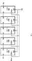
图1为示例性设备的结构框图,其包括以串行的菊花链级联排列配置的多个单端口设备110a-e。设备110a-e为示例性的存储设备,各包含有存储器(未在图中示出),该存储器可以包含动态随机存取存储器(DRAM)单元,静态随机存取存储器(SRAM)单元,闪存单元等等。每个设备110包含有串行输入(SI)、串行输出(SO),时钟(SCLK)输入以及片选择(CS#)输入。 FIG. 1 is a block diagram of an exemplary device including a plurality of single-
串行输入被用于传送信息(如命令,地址和数据信息)到设备110。串行输出被用于从设备110传出信息。SCLK输入用于向设备110提供外部的时钟信号,以及CS#输入用于向设备110提供片选信号。可与此处所述的技术一起使用的设备的一个范例是在美国专利申请第11/324,023号中的多独立串行链接(MISL)存储设备。 The serial input is used to communicate information (such as commands, addresses, and data information) to device 110 . Serial output is used to transfer information from device 110 . The SCLK input is used to provide an external clock signal to the device 110 , and the CS# input is used to provide a chip select signal to the device 110 . One example of a device that may be used with the techniques described herein is the Multiple Independent Serial Link (MISL) storage device in US Patent Application Serial No. 11/324,023. the
菊花链级联排列的设备110间的SI和SO彼此连接,以使得在菊花链级联中较前的设备110中的SO耦合到菊花链级联中下一个设备110的SI。例如,设备110a的SO连接到设备110b的SI。每个设备110的SCLK输入馈送以来自例如存储控制器(未在图中示出)的时钟信号。该时钟信号通过共同的连接分配到各个设备110。如下所述,SCLK特别被用于将输入到设备110的信息锁存到包含的各种寄存器中。 The SI and SO among devices 110 arranged in a daisy-chain cascade are connected to each other such that the SO in a device 110 earlier in the daisy-chain cascade is coupled to the SI of the next device 110 in the daisy-chain cascade. For example, the SO of
输入到设备110的信息可以在提供至SCLK输入的时钟信号的不同时刻被锁存。例如,在单数据率(SDR)实现中,通过SI输入到设备110的信息可以在SCLK时钟信号的上升沿或下降沿被锁存。可替换的,在双数据率(DDR)实现中,通过SI输入到设备110的信息在SCLK时钟信号的上升沿和下降沿都可被锁存。 Information input to device 110 may be latched at different times of the clock signal provided to the SCLK input. For example, in a single data rate (SDR) implementation, information input to device 110 via SI may be latched on either the rising or falling edge of the SCLK clock signal. Alternatively, in a double data rate (DDR) implementation, information input to device 110 via SI may be latched on both rising and falling edges of the SCLK clock signal. the
各个设备的用于选择设备的CS#输入为传统的片选择。该输入被耦合到公用链接以使得片选择信号被并行确立(assert)到所有的设备110,因而同时对所有设备110进行选择。 The CS# input of each device used to select the device is a traditional slice selection. This input is coupled to a common link so that the chip select signal is asserted to all devices 110 in parallel, thus selecting all devices 110 at the same time. the
图2为示例性设备的结构示意图,其包括以具有级联时钟的串行菊花链级联排列配置的多个单端口设备210a-e。每个设备210包括如上所述的SI,SO,SCLK输入以及CS#输入。此外,每个设备210包含时钟输出(SCLKO)。该SCLKO为将输入到设备210的SCLK信号输出的输出端。 FIG. 2 is a block diagram of an exemplary device including multiple single-
参考图2,如前所述,设备210的SI和SO以串行的菊花链级联被耦合。另外,设备的SCLK输入和SCLKO输出也以串行的菊花链级联排列被耦合,使得在菊花链级联中较前的设备210中的SCLKO耦合到菊花链级联中下一个设备210的SCLK输入。因此,例如,设备210a的SCLKO耦合到设备210b的SCLK输入。 Referring to FIG. 2, as previously described, the SI and SO of device 210 are coupled in a serial daisy-chain cascade. Additionally, the SCLK input and SCLKO output of the devices are also coupled in a serial daisy-chain cascade arrangement such that SCLKO in a device 210 earlier in the daisy-chain cascade is coupled to the SCLK of the next device 210 in the daisy-chain cascade. enter. Thus, for example, SCLKO of
注意,时钟信号在通过菊花链级联的装置传播时会产生延迟。可采用内部延迟补偿电路,如延迟锁定环(DLL)电路,来排除该延迟。 Note that the clock signal is delayed as it propagates through the daisy-chained devices. Internal delay compensation circuits, such as delay locked loop (DLL) circuits, can be used to remove this delay. the
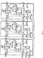
图3为示例性设备的结构示意图,其包括以串行菊花链级联排列配置的多个双端口设备310a-e。每个设备310在每个端口各包括一个SI和SO,还包括如前所述的SCLK输入和CS#输入。参考图3,设备310上第一端口的SI被标记为“SI0”,第二断口的SI被标记为“SI1”。类似的,第一端口的SO被标记为“SO0”,第二端口的SO被标记为“SO1”。每个端口的SO和SI如前所述连接于设备310之间。因此,例如,设备310a上的端口0的SO馈送到设备310b上的端口0的SI,如此等等。类似的,设备310a上的端口1的SO馈送到设备310b上的端口1的SI,如此等等。 FIG. 3 is a block diagram of an exemplary device including multiple dual-
图4为示例性设备的结构示意图,其包括以串行菊花链级联排列配置的多个单端口设备,该串行菊花链级联排列具有用于各种使能信号的输入和输出。每个设备410包含如前所述的SI、SO、CS#输入、SCLK输入。此外,每个设备410还包括输入端口使能(IPE)输入、输出端口使能(OPE)输入、输入端口使能输出(IPEQ)以及输出端口使能输出(OPEQ)。IPE输入用于向设备输入IPE信号。IPE信号由设备用来使能SI,使得IPE被确立时,信息可通过SI串行输入到设备410。类似的,OPE输入用于向设备输入OPE信号。OPE信号由设备用来使能SO,使得OPE被确立时,信息可通过SO从设备410串行输出。IPEQ和OPEQ为分别从设备输出IPE和OPE信号的输出端。IPEQ信号可以为延迟的IPE信号,或IPE信 号的变型。类似的,OPEQ信号可能为延迟的OPE信号,或OPE信号的变型。CS#输入和SCLK输入耦合到不同的链接,该链接分别分配CS#和SCLK信号到如前所述的设备410a-d。 4 is a block diagram of an exemplary device including multiple single-port devices configured in a serial daisy-chain cascade arrangement with inputs and outputs for various enable signals. Each device 410 contains SI, SO, CS# inputs, SCLK inputs as previously described. In addition, each device 410 also includes an input port enable (IPE) input, an output port enable (OPE) input, an input port enable output (IPEQ), and an output port enable output (OPEQ). The IPE input is used to input the IPE signal to the device. The IPE signal is used by the device to enable SI so that when IPE is asserted, information can be serially input to device 410 via SI. Similarly, the OPE input is used to input the OPE signal to the device. The OPE signal is used by the device to enable the SO so that when OPE is asserted, information can be serially output from the device 410 through the SO. IPEQ and OPEQ are output terminals for outputting IPE and OPE signals from the device, respectively. The IPEQ signal may be a delayed IPE signal, or a variant of the IPE signal. Similarly, the OPEQ signal may be a delayed OPE signal, or a variant of the OPE signal. The CS# input and the SCLK input are coupled to different links that distribute the CS# and SCLK signals, respectively, to
如前所述,SI以及SO从菊花链级联排列的一个设备耦合到下一个设备。此外,菊花链级联排列中的一个在前的设备410的IPEQ和OPEQ被分别耦合到菊花链级联中的下一个设备410的IPE输入和OPE输入。这种排列允许IPE和OPE信号从菊花链级联的一个设备410传送到下一个设备。 As previously mentioned, SI and SO are coupled from one device to the next in a daisy-chain cascade arrangement. Furthermore, the IPEQ and OPEQ of a preceding device 410 in the daisy-chain cascade arrangement are respectively coupled to the IPE input and OPE input of the next device 410 in the daisy-chain cascade. This arrangement allows IPE and OPE signals to be passed from one device 410 to the next in a daisy chain cascade. the
图5为示例性设备的结构示意图,其包括以串行菊花链级联排列配置的双端口设备510a-d,该串行菊花链级联排列包括用于各种使能信号的输入和输出。每个设备510包括如前所述的CS#输入、SCLK输入,以及在每个端口上包括SI、SO、IPE、OPE、IPEQ和OPEQ。端口1和端口2中的SI、SO、IPE、OPE、IPEQ和OPEQ被分别表示为SI1、SO1、IPE1、OPE1、IPEQ1和OPEQ1,以及SI2、SO2、IPE2、OPE2、IPEQ2和OPEQ2。 5 is a block diagram of an exemplary device including two-port devices 510a-d configured in a serial daisy-chain cascade arrangement including inputs and outputs for various enable signals. Each device 510 includes a CS# input, a SCLK input as previously described, and on each port SI, SO, IPE, OPE, IPEQ, and OPEQ. SI, SO, IPE, OPE, IPEQ, and OPEQ in
如上所述,各个设备510的CS#输入被耦合到单个链路以同时选择所有设备510。类似的,如上所述,各个设备510的SCLK被耦合到单个链路,以配置成同时分配时钟信号到所有设备510。并且,如上所述,SI、SO、IPE、OPE、IPEQ和OPEQ在设备间耦合,以使得菊花链级联中的一个在前设备的SO、IPEQ和OPEQ被耦合到菊花链级联中的一个在后设备的SI、IPE和OPE。例如,设备510a的SO1、SO2、IPEQ1、IPEQ2、OPEQ1和OPEQ2被分别耦合到设备510b中的SI1、SI2、IPE1、IPE2、OPE1和OPE2。 As described above, the CS# input of each device 510 is coupled to a single link to select all devices 510 simultaneously. Similarly, as described above, the SCLK of each device 510 is coupled to a single link configured to distribute the clock signal to all devices 510 simultaneously. And, as described above, SI, SO, IPE, OPE, IPEQ, and OPEQ are coupled between devices such that the SO, IPEQ, and OPEQ of a preceding device in the daisy-chain cascade are coupled to one SI, IPE, and OPE of the device behind. For example, SO1, SO2, IPEQ1, IPEQ2, OPEQ1, and OPEQ2 of device 510a are coupled to SI1, SI2, IPE1, IPE2, OPE1, and OPE2 of device 510b, respectively. the
分别输入到设备510a的SI、IPE和OPE输入端的SI、IPE和OPE信号在例如存储器控制器(未示出)的控制下,被提供给设备510a。设备510d通过设备510d中的SO、IPEQ以及OPEQ输出端向存储器控制器返回数据和控制信号。 The SI, IPE, and OPE signals respectively input to the SI, IPE, and OPE inputs of the device 510a are provided to the device 510a under the control of, for example, a memory controller (not shown). Device 510d returns data and control signals to the memory controller through the SO, IPEQ, and OPEQ outputs in device 510d. the
图6为示例性设备的结构示意图,其包括以串行菊花链级联排列配置的多个设备610a-d,该设备具有多个串行输入端(SI0到SIn)以及多个串行输出端(SO0到SOn)。此外,每个设备610具有如上所述的SCLK输入和CS#输入。 6 is a block diagram of an exemplary device including multiple devices 610a-d configured in a serial daisy-chain cascaded arrangement, the devices having multiple serial inputs (SI0 through SIn) and multiple serial outputs (SO0 to SOn). In addition, each device 610 has a SCLK input and a CS# input as described above. the
各个设备610所使用的串行输入端(SI0到SIn)以及串行输出端(SO0到SOn)使得信息以串行的方式分别输入和输出设备610。每个输入被分 配特定的角色以输入某种类型的数据(如地址,命令,数据)和/或信号(如使能信号)到设备610。类似的,每个输出被分配特定的角色以从设备610输出某种类型的数据和信号。例如,一个或多个输入可以被分配一个能将地址信息输入到设备610的角色。类似的,例如,一个或多个输出可以被分配一个将地址信息从设备610输出的角色。 The serial inputs (SI0 to SIn) and serial outputs (SO0 to SOn) used by each device 610 allow information to be input and output to and from the device 610, respectively, in a serial manner. Each input is assigned a specific role to input a certain type of data (e.g. address, command, data) and/or signal (e.g. enable signal) to device 610. Similarly, each output is assigned a specific role to output certain types of data and signals from device 610 . For example, one or more inputs may be assigned a role capable of inputting address information into device 610 . Similarly, one or more outputs may be assigned a role to output address information from device 610, for example. the
每个设备610上的串行输入端和串行输出端的数量通常取决于某些因素,例如地址线的数量,命令大小和数据宽度大小。这些因素会受到设备在特定系统应用中如何使用的影响。例如,与需要对大量信息进行数据存储的系统应用相比,需要对少量信息进行数据存储的系统应用可以采用具有较少地址线和数据线的设备,而且因此有较少的输入/输出端。 The number of serial inputs and serial outputs on each device 610 generally depends on certain factors, such as the number of address lines, command size and data width size. These factors are affected by how the device is used in a particular system application. For example, a system application requiring data storage of a small amount of information may employ a device having fewer address and data lines, and thus fewer input/output ports, than a system application requiring data storage of a large amount of information. the
图7为描述在以串行菊花链级联排列配置的单独设备上和配置的的多个设备上执行读操作时相关的时序的时序图。参考图7,CS#被确立以选择所有的设备。通过确立IPE和将与读操作相关的时钟信息通过SI按时钟节拍输入进设备以开始读操作。示例性地,这些信息包括指示执行读操作的命令(CMD)以及指示从哪里读取数据的存储器起始地址的列地址(Col ADD)和行地址(Row ADD)。 FIG. 7 is a timing diagram depicting the timing associated with performing a read operation on a single device configured in a serial daisy chain cascade arrangement and on multiple devices configured. Referring to Figure 7, CS# is asserted to select all devices. The read operation is started by establishing the IPE and inputting the clock information related to the read operation into the device according to the clock beat through the SI. Exemplarily, such information includes a command (CMD) indicating to perform a read operation, and a column address (Col ADD) and a row address (Row ADD) indicating a memory start address from where to read data. the
在时间“tR”,从存储器读取所请求的数据并将之存放在包含在设备中的特定内部数据缓存器中。tR的长度通常由包含存储器的单元的特性决定。在时间tR后,OPE被确立以使得数据从内部数据缓存器通过SO串行传输到菊花链级联的下一个设备。示例性地,在SLCK的上升沿,数据从位于SO输出端的内部缓存中串行输出。将从位于菊花链级联的设备所输出的数据延迟一个时钟周期那么长以控制例如与传播控制信号(如IPE以及OPE)相关的延迟时间(latency)。正如将要描述的,采用时钟同步锁存器执行延迟时间控制。 At time "tR", the requested data is read from memory and stored in a specific internal data buffer included in the device. The length of tR is generally determined by the characteristics of the cell containing the memory. After time tR, OPE is asserted so that data is transferred serially from the internal data buffer through SO to the next device in the daisy-chain cascade. Exemplarily, at the rising edge of SLCK, data is serially output from the internal buffer at the SO output. Delaying data output from devices located in the daisy-chain cascade by as long as one clock cycle controls, for example, the latency associated with propagating control signals such as IPE and OPE. As will be described, delay time control is performed using clocked latches. the
闪存核心架构实施中的级联存储设备的一些操作实例显示在下列表1中。表1列出了目标设备地址(TDA),可能的操作(OP)码以及列地址,行/体地址的对应状态,以及输入数据。 Some operational examples of cascaded storage devices in a flash core architecture implementation are shown in Table 1 below. Table 1 lists the target device address (TDA), possible operation (OP) codes and column addresses, corresponding states of row/body addresses, and input data. the
表1 命令集 Table 1 command set
在本发明的一些实施例中,在图1-6中所显示的系统的各个设备可拥有特有的设备识别符,以用作串行输入数据中的目标设备地址(tda)。在接收串行输入数据时,闪存设备分析串行输入数据中的目标设备地址,并通过关联目标设备地址与设备的特有的设备识别号来判断设备是否是目标设备。 In some embodiments of the present invention, each device of the system shown in FIGS. 1-6 may have a unique device identifier for use as a target device address (tda) in the serial input data. When receiving the serial input data, the flash memory device analyzes the target device address in the serial input data, and determines whether the device is the target device by associating the target device address with the unique device identification number of the device. the
表2显示了根据本发明的实施例(包括结合图1-6所描述的系统)的输入数据流的较佳输入顺序。命令、地址,以及数据,从最高有效位开始串行地移进或移出每个存储设备。 Table 2 shows the preferred input order of the input data streams according to embodiments of the present invention, including the system described in connection with FIGS. 1-6. Commands, addresses, and data are shifted in and out of each memory device serially, starting with the most significant bit. the
参考图4,设备410a-d可以在输入端口使能(IPE)为高时利用在串行时钟(SCLK)上升沿所采样的串行输入信号(SIP)进行操作。命令序列以单字节的目标设备地址(“tda”)和单字节的操作码(也可替换地称为命令码(表1中的“cmd”))开始。通过在串行输入信号的最高有效位中采用单字节目标设备地址作为起始,设备可在处理所收到的任何额外的输入数据前,先分析目标地址域。如果存储设备并非目标设备,则可在处理前传送该串行输入数据到另一个设备,从而节省额外的处理时间和资源。 Referring to FIG. 4,
表2字节模式下的输入序列 Table 2 Input sequence in byte mode
在单字节的cmd码之后,将单字节TDA移位到设备中。最高有效位(MSB)从SIP开始并于串行时钟(SCLK)的上升沿锁存各个位。取决于命令,单字节命令码之后可跟随列地址字节、行地址字节、体地址字节,数据字节,和/或组合或空白。 After the single-byte cmd code, the single-byte TDA is shifted into the device. The most significant bit (MSB) starts with the SIP and latches each bit on the rising edge of the serial clock (SCLK). Depending on the command, the single byte command code may be followed by a column address byte, a row address byte, a bank address byte, a data byte, and/or a combination or blank. the
图8为描述与在串行菊花链级联排列中所配置的设备间传送的数据有关的时序的时序图。如上所述,确立CS#以选择设备。通过确立IPE以及在连续的SCLK的上升沿将时钟数据按时钟节拍送入设备,信息被输入到串行菊花链级联排列中的第一个设备。IPE在不到一个周期的时间内通过第一设备传播到第二设备。这使得信息在按时钟节拍进入第一设备后的一个周期内从第一设备的SO按时钟节拍进入第二设备的SI。这一过程在串行菊花链级联的连续设备中重复进行。因此,例如,在从数据在第一设备的锁存点算起的SCLK的第三个上升沿时,将信息输入到串行菊花链级联中的第三设备。 8 is a timing diagram depicting the timing associated with data transfer between devices configured in a serial daisy chain cascaded arrangement. As above, CS# is asserted to select the device. Information is input to the first device in a serial daisy-chain cascade arrangement by asserting IPE and clocking data into the device on successive rising edges of SCLK. The IPE propagates through the first device to the second device in less than one cycle. This allows information to be clocked from the SO of the first device into the SI of the second device within one cycle of clocking into the first device. This process is repeated in successive devices in a serial daisy chain cascade. So, for example, information is input to a third device in a serial daisy chain cascade on the third rising edge of SCLK counting from the point at which data is latched at the first device. the
图9为单端口设备中的示例性串行输出控制逻辑900的框图。逻辑900包括用于IPE的输入缓存器902、用于SI(SIP)的输入缓存器904、用于 OPE的输入缓存器906、输入锁存控制器908、串行至并行寄存器910、输出锁存控制器912、数据寄存器914、地址寄存器916、命令解释器918、选择器920、页缓存器924、逻辑或(OR)门926、输出缓存器928、选择器930以及存储器950。 FIG. 9 is a block diagram of exemplary serial
输入缓存器902是一种传统的低电压晶体管到晶体管逻辑(LVTTL)缓存器,它被配置成缓存馈送给设备位于缓存器902的输入端的IPE信号的状态。缓存器902的输出提供给输入锁存控制器908,它锁存IPE信号的状态并向输入缓存器904和选择器920提供IPE信号的锁存的状态。输入缓存器904是一种LVTTL缓存器,它被配置成缓存通过SI输入提供给设备的信息。输入缓存器904由输入锁存控制器908使能。当被使能时,提供给SI输入的信息由缓存器908传送到串行至并行寄存器910以及选择器930的一个输入。当由输入锁存控制器908所提供的IPE信号的锁存的状态显示IPE信号被确立时,输入缓存器904被使能。提供给串行至并行寄存器910的信息由寄存器910从串行形式转换为并行形式。串行至并行寄存器910的输出提供给数据寄存器914,地址寄存器916以及命令解释器918。 The
数据寄存器914以及地址寄存器916分别保存通过SI提供给设备的数据以及地址信息。命令解释器918被配置成解释通过SI输入到设备的命令。这些命令用于进一步控制设备的操作。例如,“写存储器”命令可被用于令设备将包含于数据寄存器914的数据写入位于设备中经由地址寄存器916所指定地址的存储器950。 The data register 914 and the
输入缓存器906为LVTTL缓存器,它被配置成缓存提供给设备的OPE输入的OPE信号。缓存器906的输出被传送到用于锁存OPE信号的状态的输出锁存控制器912。输出锁存控制器输出锁存的OPE信号状态到或门926。或门926为传统的逻辑或门,其输出被用于使能/禁止输出缓存器928的输出。 The
选择器920为传统的2选1多路复用器,它通过信号DAISY_CHAIN从两个输入中选择其一作为输出。如前所述,这些输入之一为从输入锁存控制器908所得到的IPE信号的锁存状态。另一个输入被设定为逻辑低状态。信号DAISY_CHAIN显示设备是否以串行菊花链级联排列连接到一个或多个其它设备。示例性地,如果设备以串行菊花链级联排列连接到一个或多个其它设备,该信号被确立。确立DAISY_CHAIN信号使得提供给选 择器920的IPE信号的锁存状态从选择器920输出。当DAISY_CHAIN信号未被确立时,输入到选择器920的逻辑低状态从选择器920被输出。 The
页缓存器924为传统的数据缓存器,它被配置为保存从存储器950读得的信息。选择器930为传统的2选1多路复用器,通过信号ID_MATCH从两个输入中选择一个作为输出。选择器930的一个输入由页缓存器924的输出提供,另一个输入由SI输入缓存器904的输出提供。选择器930的输出提供给输出缓存器928。信号ID_MATCH指示通过SI传送到设备的特定命令是否寻址(addressed)到该设备。如果该命令寻址到设备,ID_MATCH被确立以使得页缓存器924的输出从选择器930输出。如果ID_MATCH未被确立,则从SI缓存器904得到的输出(即,输入到设备的SI信号的状态)从选择器930输出。
存储器950为传统的寄存器,它被配置成保存数据。存储器950可以是包含多个单元的随机存取存储器(RAM),如静态RAM(SRAM),动态RAM(DRAM)或闪存单元,其可使用通过SI输入到设备的地址进行寻址。
在操作时方面,一个确立的IPE信号由输入缓存器902进行缓存并被传送到输入锁存控制器908,该控制器锁存所确立的IPE的状态。这一锁存状态提供给选择器920以及输入缓存器904,以使能该缓存器904。输入至输入缓存器904的命令、地址以及数据信息然后被传送到用于将信息从串行形式转换到并行形式的串行至并行寄存器910,并分别将命令、地址以及数据信息提供给命令解释器918、地址寄存器916和数据寄存器914。缓存器904的输出也被提供给选择器930。如果ID_MATCH未被确立,缓存器904的输出会出现在选择器930的输出,该输出被提供给输出缓存器928的输入。如果DAISY_CHAIN被确立,IPE的锁存状态会出现在选择器920的输出,并提供给或门926的第一输入。或门926传递IPE的状态到输出缓存器928以使能输出缓存器928。这又将允许输入到SI输入端的信息从设备的SO输出。 In operation, an asserted IPE signal is buffered by the
通过确立OPE以及ID_MATCH,将来自页缓存器924的数据从设备输出。详细的说,所确立的OPE的状态提供给输入缓存器906,该缓存器又提供该状态到用于锁存该状态的输出锁存控制器912。锁存的所确立的状态被提供给或门926的第二输入,或门926输出信号以使能输出缓存器928。确立ID_MATCH使能页缓存器924的输出出现在选择器930的输出。选择器930的输出被提供给所使能的输出缓存器928,该缓存器从设备的SO输出端将数据输出该设备。 By asserting OPE and ID_MATCH, data from the
注意,如果DAISY_CHAIN未被确立,输出缓存器928仅被OPE使能。这将允许该设备在非菊花链串行级联结构中使用。 Note that
图10为双端口设备中的示例性串行输出控制逻辑1000的框图。对于每个端口,该串行输出控制逻辑1000包括IPE输入缓存器1002、SI输入缓存器1004、OPE输入缓存器1006、输入锁存控制器1008、串行到并行寄存器1010、输出锁存控制器1012、数据寄存器1014、地址寄存器1016、命令解释器1018、选择器1020、页缓存器1024、逻辑或门1026、输出缓存器1028和选择器1030,它们分别与上述的IPE输入缓存器902、SIP输入缓存器904、OPE输入缓存器906、输入锁存控制器908、串行至并行寄存器910、输出锁存控制器912、数据寄存器914、地址寄存器916、命令解释器918、选择器920、页缓存器924、逻辑或门926、输出缓存器928和选择器930相同。 FIG. 10 is a block diagram of exemplary serial output control logic 1000 in a dual port device. For each port, the serial output control logic 1000 includes IPE input buffer 1002, SI input buffer 1004, OPE input buffer 1006, input latch controller 1008, serial to parallel register 1010, output latch controller 1012, data register 1014, address register 1016, command interpreter 1018, selector 1020, page buffer 1024, logical OR gate 1026, output buffer 1028 and selector 1030, which are respectively connected with the above-mentioned
图11为与此处所描述的技术一同使用的串行输出控制逻辑1100的另一个实施例的详细框图。逻辑1100包括SI输入缓存器1104、IPE输入缓存器1106、OPE输入缓存器1108、SCLK输入缓存器1110、逻辑与(AND)门1112和1114、锁存器1116、1118、1120和1122、选择器1124和1130、逻辑或门1126和SO输出缓存器1128。缓存器1104、1106、1108和1110为传统的LVTTL缓存器,分别配置为缓存被输入到设备中的SI、IPE、OPE和SCLK信号。 FIG. 11 is a detailed block diagram of another embodiment of serial
与门1112被配置为当IPE被确立时,将输入到SI的信息输出到锁存器1116。锁存器1116被配置为当缓存器1110提供时钟信号(SCLK)时,锁存该信息。DATA_OUT表示从包含在设备内存储器(未示出)所读取的数据的状态。与门1114被配置为当OPE被确立时,输出DATA_OUT的状态。与门1114的输出提供给锁存器1118,所述的锁存器1118被配置为当缓存器1110提供时钟信号时锁存DATA_OUT的状态。缓存器1106被配置为缓存提供给设备的IPE信号。缓存器1106的输出被锁存器1120锁存。类似的,缓存器1108被配置为缓存提供给设备的OPE信号。锁存器1122被配置为锁存由缓存器1108所输出的OPE的状态。选择器1124和1130为传统的2选1多路复用器,各包含两个输入。选择器1124的输入通过上述的ID_MATCH信号被选择从选择器1124作为输出。一个输入被 提供由锁存器1118所维持的DATA_OUT的锁存状态。当ID_MATCH被确立时,这一输入被选择从选择器1124输出。另一输入被提供由锁存器1116所维持的SI的锁存状态。当ID_MATCH未被确立时,这一输入被选择从选择器1124输出。 AND
选择器1130的输入通过上述的DAISY_CHAIN信号被选择从选择器1130输出。选择器1130的一个输入被提供由锁存器1120所维持的IPE的锁存状态,而另一个输入连接到逻辑0。当DAISY_CHAIN被确立时,IPE的锁存状态被选择作为选择器1130的输出。类似的,当DAISY_CHAIN未被确立时,逻辑0被选择从选择器1130的输出。 The input of the
或门1126为传统的逻辑或门,它被配置为向输出缓存器1128提供使能/禁止信号。或门1126被提供选择器1130的输出,以及由锁存器1122所维持的OPE的锁存状态。这两个输出的任一个可被用于向缓存器1128提供时能信号以使能该缓存器的输出。缓存器1128为传统的缓存器,它用来缓存输出信号SO。如上所述,缓存器1128通过或门1126的输出被使能/禁止。 The
在操作方面,当IPE被确立时,通过SI被输入到设备的信息被提供给锁存器1116。示例性地,锁存器1116在IPE被确立后的SCLK的第一向上转变时锁存该信息。类似的,锁存器1120在这次SCLK转变时锁存IPE的状态。假设ID_MATCH未被确立,锁存器1116的输出通过选择器1124被提供给缓存器1128。类似的,确立的IPE从缓存器1106被传送到锁存器1120,在锁存器1120中也示例性地在SCLK的第一向上转变时进行锁存。假设DAISY_CHAIN被确立时,IPE的锁存状态被提供到选择器1130的输出,并被传送到或门1126以向缓存器1128提供使能信号。接着,SI的锁存状态通过缓存器1128从设备传出作为输出SO。 In terms of operation, when IPE is asserted, information that is input to the device via SI is provided to latch 1116 . Illustratively,
当DAISY_CHAIN未被确立时,选择输入到选择器1130的逻辑0,从选择器1130输出逻辑0。这有效地禁止了IPE使能缓存器1128。 When DAISY_CHAIN is not asserted,
示例性地,在OPE被确立后的SCLK的下一个向上转变时,OPE的所确立的状态被锁存在锁存器1122,以及DATA_OUT的状态被锁存在锁存器1118。假设ID_MATCH被确立,DATA_OUT的锁存状态被选择器1124选择并被加到缓存器1128的输入。同时,从锁存器1122得到的OPE的锁存的所确立的状态通过或门1126传送到使能缓存器1128,这使得DATA_OUT的锁存状态从设备输出作为输出SO。 Illustratively, on the next up transition of SCLK after OPE is asserted, the asserted state of OPE is latched in
图12为以串行菊花链级联排列配置以及包括示例性的串行输出控制逻辑的设备的示例性结构框图。该排列包括三个设备1210,其如前所述被配置成菊花链级联中的一个在先设备的输出端与菊花链级联中的下一个设备的输入端相耦合。信息和数据从一个设备到下一个设备的传送过程参考下面的图13进行描述。 12 is an exemplary block diagram of a device configured in a serial daisy-chain cascade arrangement and including exemplary serial output control logic. The arrangement includes three devices 1210 configured as previously described such that the output of a previous device in the daisy-chain cascade is coupled to the input of the next device in the daisy-chain cascade. The transfer of information and data from one device to the next is described with reference to Figure 13 below. the
图13为用于说明在图12中所描述设备的输入和输出相关时序的示例性时序图。具体来说,关于将在每个设备1210的SI输入端所输入的信息传送到设备1210的SO输出端,该图描述了各设备中的串行输出控制逻辑1100的操作。 FIG. 13 is an exemplary timing diagram for explaining input and output related timing of the device described in FIG. 12 . Specifically, the figure depicts the operation of the serial
参考图11、12和13,假设DAISY_CHAIN被确立。当在设备1210a确立IPE时,如前所述在设备SI输入端的数据通过设备的串行输出控制逻辑1100传送到设备1210a的SO输出端。详细的,在IPE被确立后的每个SCLK上升沿,数据被示例性地按时钟节拍输入进设备1210a中。如前所述IPE的信息和状态通过逻辑1100传播,并分别在设备的SO和IPEQ输出端离开设备1210a。这些输出在图中分别用S1和P1表示。如前所述,这些输出被提供给设备1210b的SI和IPE输入,通过设备1210b的串行输出控制逻辑1100,并在一个时钟周期后自设备1210b的SO和IPEQ输出端从设备1210b输出。这些输出在图中分别用S2和P2表示。类似的,设备1210b的SO和IPEQ输出分别被提供给设备1210c的SI和IPE输入,通过设备1210c的串行输出控制逻辑1100,并在一个时钟周期后分别从设备的SO和IPEQ输出端从设备1210c输出。这些输出在图中分别用S3和P3表示。 Referring to Figures 11, 12 and 13, it is assumed that DAISY_CHAIN is established. When IPE is asserted at
在如上所述的菊花链级联排列中,对于SDR操作在菊花链级联中的信号输出延迟时间(latency)可以采用下面的公式确定: In the above-mentioned daisy-chain cascade arrangement, the signal output delay time (latency) of the SDR operation in the daisy-chain cascade can be determined by the following formula:
output_latency=N*clock_cycle_time output_latency=N*clock_cycle_time
其中: in:
“output_latency”是数据的输出延迟时间, "output_latency" is the output delay time of the data,
“N”是菊花链级联排列中的设备的数量,以及 "N" is the number of devices in the daisy-chain cascaded arrangement, and
“clock_cycle_time”是时钟操作的时钟周期时间。 "clock_cycle_time" is the clock cycle time of the clock operation. the
例如,假设图12中所描述的菊花链级联的clock_cycle_time为10纳秒。对于在设备1210c中的SO的数据,总输出延迟时间为3*10纳秒或30纳秒。 For example, assume that the clock_cycle_time of the daisy-chain cascade depicted in Figure 12 is 10 nanoseconds. For the data of the SO in device 1210c, the total output delay time is 3*10 ns or 30 ns. the
在DDR操作的例子中,输出延迟时间可以通过如下方式决定: In the example of DDR operation, the output delay time can be determined as follows:
output_latency=N*(clock_cycle_time/2) output_latency=N*(clock_cycle_time/2)
在DDR操作中,时钟的两沿都可作为输入数据的锁存点和输出数据的改变点。因此,总的延迟时间是SDR操作中延迟时间的一半。 In DDR operation, both edges of the clock can be used as the latch point of input data and the change point of output data. Therefore, the total delay time is half of the delay time in SDR operation. the
注意,在上述的说明中,对于SDR操作输入到设备1210中的信息在一个时钟周期后输出,对于DDR操作在半个周期后输出。引入此类延迟以提供启动输出缓存器1128所需的时间。 Note that in the above description, the information input into the device 1210 is output after one clock cycle for SDR operation, and after half a cycle for DDR operation. Such a delay is introduced to provide the time required for the
图14为用于将菊花链级联中的第一设备1450a的存储器所存储的数据传送到菊花链级联中的第二设备1450b的逻辑1400的框图。逻辑1400包括数据输出寄存器1402,OPE输入缓存器1404,SCLK输入缓存器1406,与门1408,数据输出锁存器1410,OPE状态锁存器1412,选择器1414,SO输出缓存器1416以及OPEQ输出缓存器1418。 14 is a block diagram of
数据输出寄存器1402为传统的寄存器,它被配置为存储自包含于设备1450中的存储器所读取的数据。寄存器1402示例性地为并行至串行数据寄存器,它以并行方式从存储器加载数据并将数据串行传输到门1408的输入端。SCLK提供了寄存器1402用来传送数据到门1408时所采用的时钟信号。如所示,数据寄存器1402被配置为保存包括位D0到D7的字节数据,其中D0为字节中的最低有效位(LSB),而位D7为字节中的最高有效位(MSB)。寄存器1402以并行方式从存储器加载一字节宽度的数据。该数据从最高有效位开始从寄存器移出并以串行方式逐位地提供给门1408的输入。
缓存器1404和1406为传统的LVTTL缓存器,分别用于缓存输入信号OPE和SCLK。OPE信号从缓存器1404的输出(OPEI)传送到门1408。将SCLK信号从缓存器1406的输出传送到数据输出寄存器1402,以及锁存器1410和1412,以向这些组件提供时钟。 The
门1408为传统的逻辑与门,它被配置为当OPE被确立时传送数据输出寄存器1402的输出(DATA_OUT)到锁存器1410。门1408的输出被表示为“DBIT”。锁存器1410和1412为传统的锁存器,它被配置为分别锁存DBIT和OPE信号的状态。选择器1414为传统的2选1多路复用器,它由信号ID_MATCH控制。其中一个数据输入为DBIT的锁存状态。当ID_MATCH被确立时,这一状态从选择器1414输出。另一输入为通过设备1450a的SI传输到该设备的串行数据(SI0)。当ID_MATCH未被确立 时,这一信息从选择器1414中输出。
缓存器1416和1418为传统的缓存器,它们被配置为分别缓存选择器1414和锁存器1406的输出。缓存器1416的输出作为SO(SO0)离开设备1450a以及缓存器1418的输出作为OPEQ(OPEQ0)离开设备1450a。
图15为与采用逻辑1400将一字节宽度的数据从包含在设备1450a的存储器传送到设备1450b的示例性时序相关的时序图。参考图14和15,在OPE于输入缓存器1404提供给设备1450a后不久,OPEI被确立。OPEI被提供给门1408以使能当前位于数据输出寄存器1402的D7的数据在SCLK的下一个上升沿在锁存器1410中被锁存。此外,该SCLK的下一个上升沿令数据右移进数据输出寄存器,以使得D6的数据移动到D7,D5的数据移动到D6,依此类推。锁存器1410的输出出现在选择器1414,假设ID_MATCH被确立,选择器1414输出数据的锁存状态到缓存器1416。缓存器1416将这一锁存状态作为SO0从设备1450a输出,SO0被提供给菊花链级联中的下一个设备的SI输入(SI1)。同时,同样在OPE被确立后的第一时钟的上升沿,OPE的状态在锁存器1412中被锁存。锁存器1412的输出被传送到缓存器1418,该缓存器将OPE的锁存状态作为OPEQ(OPEQ0)从设备1450a输出,该OPEQ被提供给菊花链级联中的下一个设备1450b的OPE输入(OPE1)。对比特位D6到D0重复上述过程。 15 is a timing diagram related to an exemplary timing of transferring one byte wide data from memory contained in
虽然已经参照本发明的较佳实施例特别显示与描述本发明,但本领域的技术人员应当了解到在形式与细节上可以进行的各种变化,而不脱离所附权利要求所要保护的范围。 While the invention has been particularly shown and described with reference to preferred embodiments thereof, those skilled in the art will recognize that various changes may be made in form and detail without departing from the scope of the appended claims. the
Claims (28)
Translated fromChinesePriority Applications (1)
| Application Number | Priority Date | Filing Date | Title |
|---|---|---|---|
| CN201210074088.2ACN102750975B (en) | 2005-09-30 | 2006-09-29 | Daisy chain cascading devices |
Applications Claiming Priority (9)
| Application Number | Priority Date | Filing Date | Title |
|---|---|---|---|
| US72236805P | 2005-09-30 | 2005-09-30 | |
| US60/722,368 | 2005-09-30 | ||
| US11/324,023 | 2005-12-30 | ||
| US11/324,023US7652922B2 (en) | 2005-09-30 | 2005-12-30 | Multiple independent serial link memory |
| US78771006P | 2006-03-28 | 2006-03-28 | |
| US60/787,710 | 2006-03-28 | ||
| US11/496,278US20070076502A1 (en) | 2005-09-30 | 2006-07-31 | Daisy chain cascading devices |
| US11/496,278 | 2006-07-31 | ||
| PCT/CA2006/001607WO2007036048A1 (en) | 2005-09-30 | 2006-09-29 | Daisy chain cascading devices |
Related Child Applications (1)
| Application Number | Title | Priority Date | Filing Date |
|---|---|---|---|
| CN201210074088.2ADivisionCN102750975B (en) | 2005-09-30 | 2006-09-29 | Daisy chain cascading devices |
Publications (2)
| Publication Number | Publication Date |
|---|---|
| CN101278352A CN101278352A (en) | 2008-10-01 |
| CN101278352Btrue CN101278352B (en) | 2012-05-30 |
Family
ID=39996580
Family Applications (5)
| Application Number | Title | Priority Date | Filing Date |
|---|---|---|---|
| CNA2006800364622APendingCN101278354A (en) | 2005-09-30 | 2006-09-29 | Multiple independent serial link memories |
| CN201910406571.8APendingCN110096469A (en) | 2005-09-30 | 2006-09-29 | Multiple independent serial link memories |
| CN201710560551.7APendingCN107358974A (en) | 2005-09-30 | 2006-09-29 | Multiple independent serial link memories |
| CN200680036482XAExpired - Fee RelatedCN101278352B (en) | 2005-09-30 | 2006-09-29 | Daisy chain cascade device and method |
| CN201910482688.4APendingCN110047528A (en) | 2005-09-30 | 2006-09-29 | Multiple independent serial link memories |
Family Applications Before (3)
| Application Number | Title | Priority Date | Filing Date |
|---|---|---|---|
| CNA2006800364622APendingCN101278354A (en) | 2005-09-30 | 2006-09-29 | Multiple independent serial link memories |
| CN201910406571.8APendingCN110096469A (en) | 2005-09-30 | 2006-09-29 | Multiple independent serial link memories |
| CN201710560551.7APendingCN107358974A (en) | 2005-09-30 | 2006-09-29 | Multiple independent serial link memories |
Family Applications After (1)
| Application Number | Title | Priority Date | Filing Date |
|---|---|---|---|
| CN201910482688.4APendingCN110047528A (en) | 2005-09-30 | 2006-09-29 | Multiple independent serial link memories |
Country Status (1)
| Country | Link |
|---|---|
| CN (5) | CN101278354A (en) |
Cited By (1)
| Publication number | Priority date | Publication date | Assignee | Title |
|---|---|---|---|---|
| CN108388492A (en)* | 2018-03-20 | 2018-08-10 | 珠海格力电器股份有限公司 | Multi-DSP chip debugging control method and device |
Families Citing this family (29)
| Publication number | Priority date | Publication date | Assignee | Title |
|---|---|---|---|---|
| US8307180B2 (en) | 2008-02-28 | 2012-11-06 | Nokia Corporation | Extended utilization area for a memory device |
| US7957173B2 (en)* | 2008-10-14 | 2011-06-07 | Mosaid Technologies Incorporated | Composite memory having a bridging device for connecting discrete memory devices to a system |
| US8874824B2 (en) | 2009-06-04 | 2014-10-28 | Memory Technologies, LLC | Apparatus and method to share host system RAM with mass storage memory RAM |
| US8966208B2 (en)* | 2010-02-25 | 2015-02-24 | Conversant Ip Management Inc. | Semiconductor memory device with plural memory die and controller die |
| CN102236630A (en)* | 2010-04-29 | 2011-11-09 | 鸿富锦精密工业(深圳)有限公司 | Multi-equipment connecting system |
| CN102479054B (en)* | 2010-11-22 | 2015-01-07 | 北京兆易创新科技股份有限公司 | Read-write system and method of memory chip |
| JP5323170B2 (en)* | 2011-12-05 | 2013-10-23 | ウィンボンド エレクトロニクス コーポレーション | Nonvolatile semiconductor memory and data reading method thereof |
| US9417998B2 (en) | 2012-01-26 | 2016-08-16 | Memory Technologies Llc | Apparatus and method to provide cache move with non-volatile mass memory system |
| US9311226B2 (en) | 2012-04-20 | 2016-04-12 | Memory Technologies Llc | Managing operational state data of a memory module using host memory in association with state change |
| CN103379028B (en)* | 2012-04-24 | 2016-06-22 | 宏碁股份有限公司 | Data routing system and method for daisy chain serial devices |
| US9164560B2 (en)* | 2012-05-01 | 2015-10-20 | Maxim Integrated Products, Inc. | Daisy chain configuration for power converters |
| EP2665231B1 (en)* | 2012-05-16 | 2017-07-05 | Alcatel Lucent | A method and computer program products for routing a data unit |
| CN103678222A (en)* | 2012-08-31 | 2014-03-26 | 宏碁股份有限公司 | Stacked Electronics System |
| JP5853973B2 (en)* | 2013-03-07 | 2016-02-09 | ソニー株式会社 | Storage control device, storage device, information processing system, and storage control method |
| WO2014193592A2 (en)* | 2013-05-29 | 2014-12-04 | Sandisk Technologies Inc. | High performance system topology for nand memory systems |
| US9766823B2 (en) | 2013-12-12 | 2017-09-19 | Memory Technologies Llc | Channel optimized storage modules |
| CN104750584B (en)* | 2013-12-26 | 2018-11-30 | 华邦电子股份有限公司 | Semiconductor storage and system start method |
| CN108694249B (en)* | 2018-05-30 | 2022-02-25 | 平安科技(深圳)有限公司 | Data processing method, data processing device, computer equipment and storage medium |
| KR102461751B1 (en)* | 2018-07-31 | 2022-11-02 | 에스케이하이닉스 주식회사 | Memory device and operating method thereof |
| CN111009272B (en)* | 2019-11-18 | 2020-08-25 | 广东高云半导体科技股份有限公司 | Input/output logic circuit, physical layer interface module, FPGA chip and storage system |
| CN111522759B (en)* | 2020-04-16 | 2021-10-01 | 山东智岩探测科技有限公司 | Device and method for converting multi-path synchronous serial data bus into parallel data bus |
| CN111526399A (en)* | 2020-04-29 | 2020-08-11 | 北京汽车股份有限公司 | Vehicle-mounted infotainment system, vehicle and communication method of vehicle-mounted infotainment system |
| US11094372B1 (en)* | 2020-05-07 | 2021-08-17 | Powerchip Semiconductor Manufacturing Corporation | Partial writing method of dram memoryl device to reduce power consumption associated with large voltage swing of internal input/output lines |
| CN111391512B (en)* | 2020-05-15 | 2021-09-07 | 珠海艾派克微电子有限公司 | Consumable chip and consumable |
| CN111897512A (en)* | 2020-07-28 | 2020-11-06 | 北京中星微电子有限公司 | Configurable multi-port FIFO memory |
| CN112235127B (en)* | 2020-09-22 | 2023-01-20 | 深圳优地科技有限公司 | Node fault reporting method and device, terminal equipment and storage medium |
| CN112737789A (en)* | 2020-12-23 | 2021-04-30 | 上海芯钛信息科技有限公司 | Method for realizing high-speed cryptographic operation of vehicle-mounted communication gateway based on two-way SPI (Serial peripheral interface) concurrency |
| GB2603516A (en)* | 2021-02-05 | 2022-08-10 | Aptiv Tech Ltd | Apparatus and method for serial data communication between a master device and peripheral devices |
| CN115168282B (en)* | 2022-09-08 | 2022-12-02 | 江西萤火虫微电子科技有限公司 | Method, system, equipment and storage medium for processing configuration data on bus protocol |
Family Cites Families (4)
| Publication number | Priority date | Publication date | Assignee | Title |
|---|---|---|---|---|
| AU2001243463A1 (en)* | 2000-03-10 | 2001-09-24 | Arc International Plc | Memory interface and method of interfacing between functional entities |
| CN1278239C (en)* | 2002-01-09 | 2006-10-04 | 株式会社瑞萨科技 | Storage system and storage card |
| WO2003085677A1 (en)* | 2002-04-05 | 2003-10-16 | Renesas Technology Corp. | Nonvolatile storage device |
| JP4791696B2 (en)* | 2004-03-02 | 2011-10-12 | オンセミコンダクター・トレーディング・リミテッド | Data transfer memory and module |
- 2006
- 2006-09-29CNCNA2006800364622Apatent/CN101278354A/enactivePending
- 2006-09-29CNCN201910406571.8Apatent/CN110096469A/enactivePending
- 2006-09-29CNCN201710560551.7Apatent/CN107358974A/enactivePending
- 2006-09-29CNCN200680036482XApatent/CN101278352B/ennot_activeExpired - Fee Related
- 2006-09-29CNCN201910482688.4Apatent/CN110047528A/enactivePending
Cited By (1)
| Publication number | Priority date | Publication date | Assignee | Title |
|---|---|---|---|---|
| CN108388492A (en)* | 2018-03-20 | 2018-08-10 | 珠海格力电器股份有限公司 | Multi-DSP chip debugging control method and device |
Also Published As
| Publication number | Publication date |
|---|---|
| CN110096469A (en) | 2019-08-06 |
| CN101278352A (en) | 2008-10-01 |
| CN107358974A (en) | 2017-11-17 |
| CN101278354A (en) | 2008-10-01 |
| CN110047528A (en) | 2019-07-23 |
Similar Documents
| Publication | Publication Date | Title |
|---|---|---|
| CN101278352B (en) | Daisy chain cascade device and method | |
| TWI564906B (en) | Daisy chain cascading devices | |
| US9490014B2 (en) | Method and system for accessing a flash memory device | |
| HK1178311A (en) | Daisy chain cascading devices |
Legal Events
| Date | Code | Title | Description |
|---|---|---|---|
| C06 | Publication | ||
| PB01 | Publication | ||
| C10 | Entry into substantive examination | ||
| SE01 | Entry into force of request for substantive examination | ||
| C14 | Grant of patent or utility model | ||
| GR01 | Patent grant | ||
| C56 | Change in the name or address of the patentee | Owner name:CONVERSANT INTELLECTUAL PROPERTY MANAGEMENT INC. Free format text:FORMER NAME: MOSAID TECHNOLOGIES INC. | |
| CP01 | Change in the name or title of a patent holder | Address after:Ontario, Canada Patentee after:MOSAID TECHNOLOGIES Inc. Address before:Ontario, Canada Patentee before:Mosaid Technologies Inc. | |
| CF01 | Termination of patent right due to non-payment of annual fee | ||
| CF01 | Termination of patent right due to non-payment of annual fee | Granted publication date:20120530 Termination date:20210929 |